25
Interconnect Synthesis
| Date post: | 30-Dec-2015 |
| Category: |
Documents |
| Upload: | modesta-curtis |
| View: | 42 times |
| Download: | 1 times |
Interconnect Synthesis
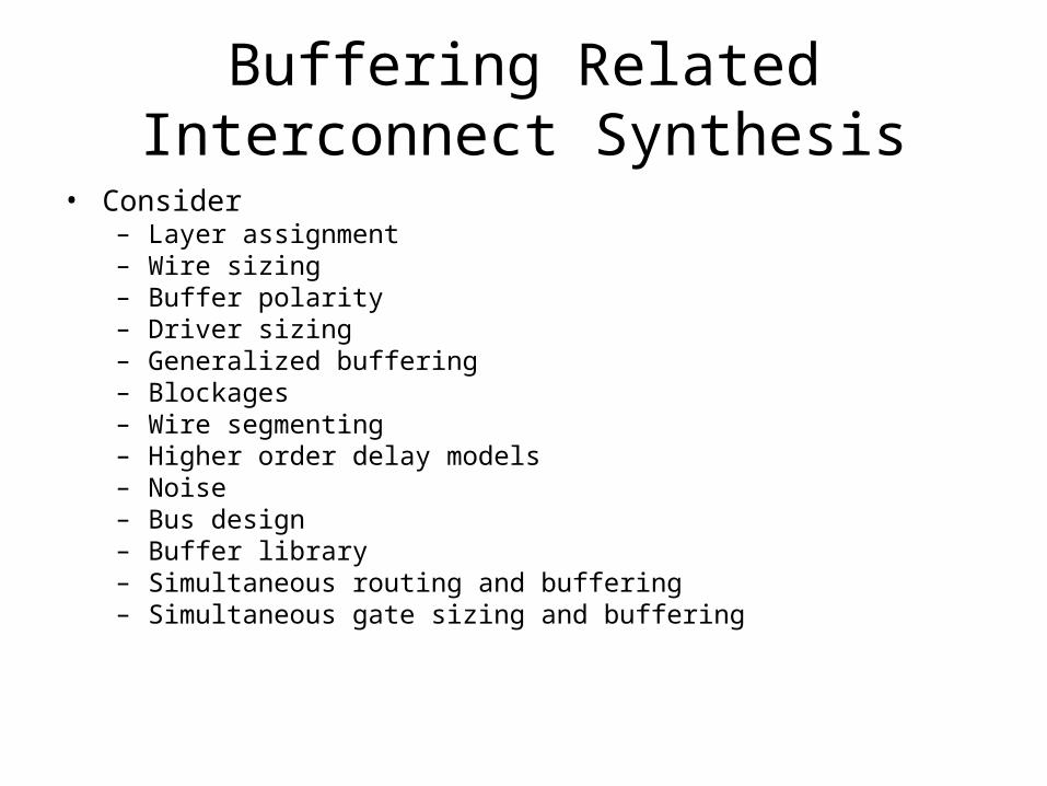
Buffering Related Interconnect Synthesis
bull Considerndash Layer assignmentndash Wire sizingndash Buffer polarityndash Driver sizingndash Generalized bufferingndash Blockagesndash Wire segmentingndash Higher order delay modelsndash Noisendash Bus designndash Buffer libraryndash Simultaneous routing and bufferingndash Simultaneous gate sizing and buffering
3
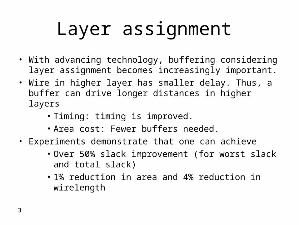
Layer assignment
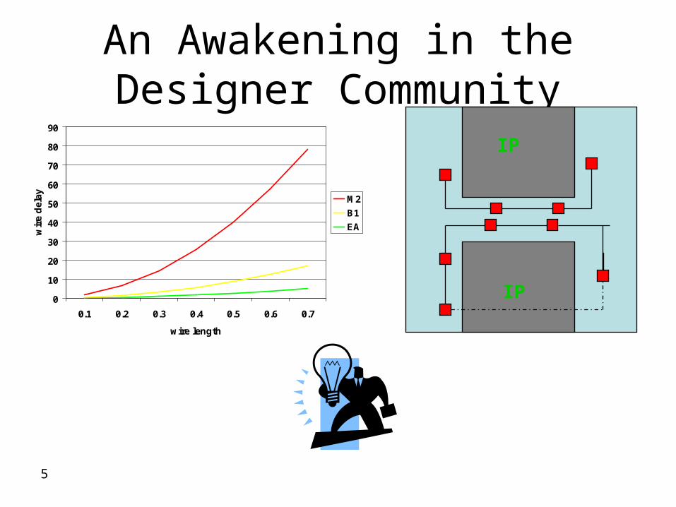
bull With advancing technology buffering considering layer assignment becomes increasingly important
bull Wire in higher layer has smaller delay Thus a buffer can drive longer distances in higher layers
bull Timing timing is improved
bull Area cost Fewer buffers needed
bull Experiments demonstrate that one can achieve
bull Over 50 slack improvement (for worst slack and total slack)
bull 1 reduction in area and 4 reduction in wirelength
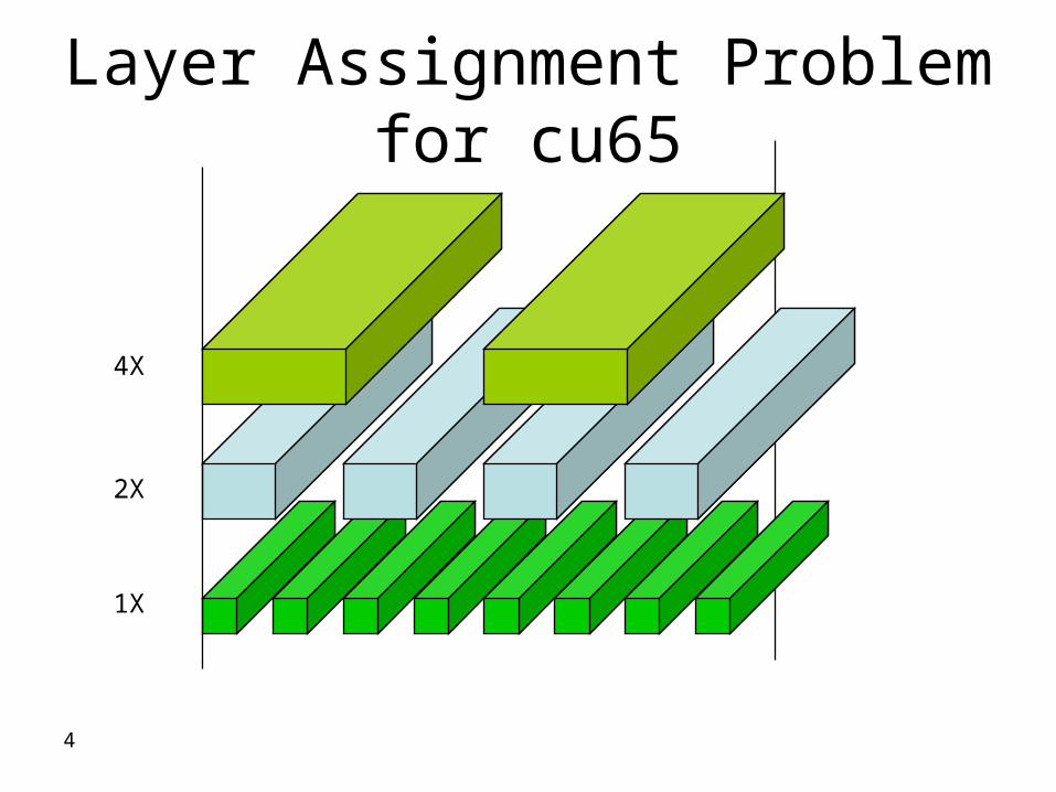
4
Layer Assignment Problem for cu65
1X
2X
4X
5
An Awakening in the Designer Community
IP
IP0
10
20
30
40
50
60
70
80
90
01 02 03 04 05 06 07
wire length
wir
e d
elay M2
B1
EA
6
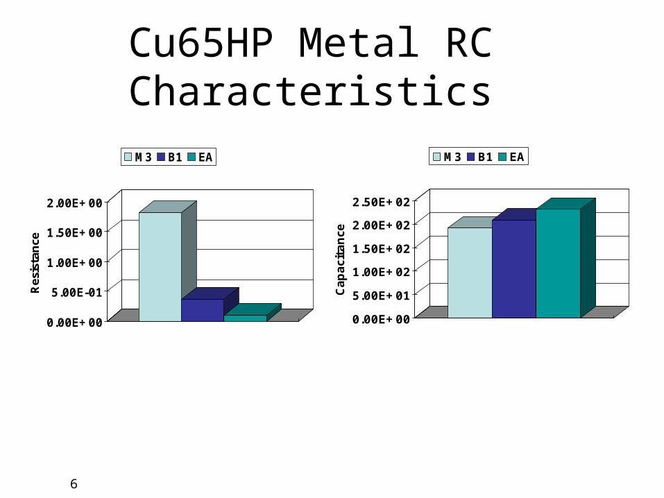
Cu65HP Metal RC Characteristics
000E+00
500E-01
100E+00
150E+00
200E+00
Res
ista
nce
M3 B1 EA
000E+00
500E+01
100E+02
150E+02
200E+02
250E+02
Capaci
tance
M3 B1 EA
7
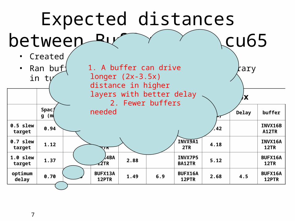
Expected distances between Buffers for cu65
bull Created a very long 2-pin net for cu65bull Ran buffopt using each buffer from the library in turn
1x 2x 4x
Spacing (mm)
Delay BufferSpacing
(mm)Delay Buffer
Spacing (mm)
Delay buffer
05 slew target
094BUFX11BA12TR
199BUFX16BA12TR
342INVX16BA12TR
07 slew target
112INVX4BA
12TR 233
INVX9A12TR
418INVX16A
12TR
10 slew target
137INVX4BA
12TR 288
INVX7P5BA12TR
512BUFX16A12TR
optimum delay
070 135BUFX13A12PTR
149 69BUFX16A12PTR
268 45BUFX16A12PTR
1 A buffer can drive longer (2x-35x) distance in higher layers with better delay
2 Fewer buffers needed
8
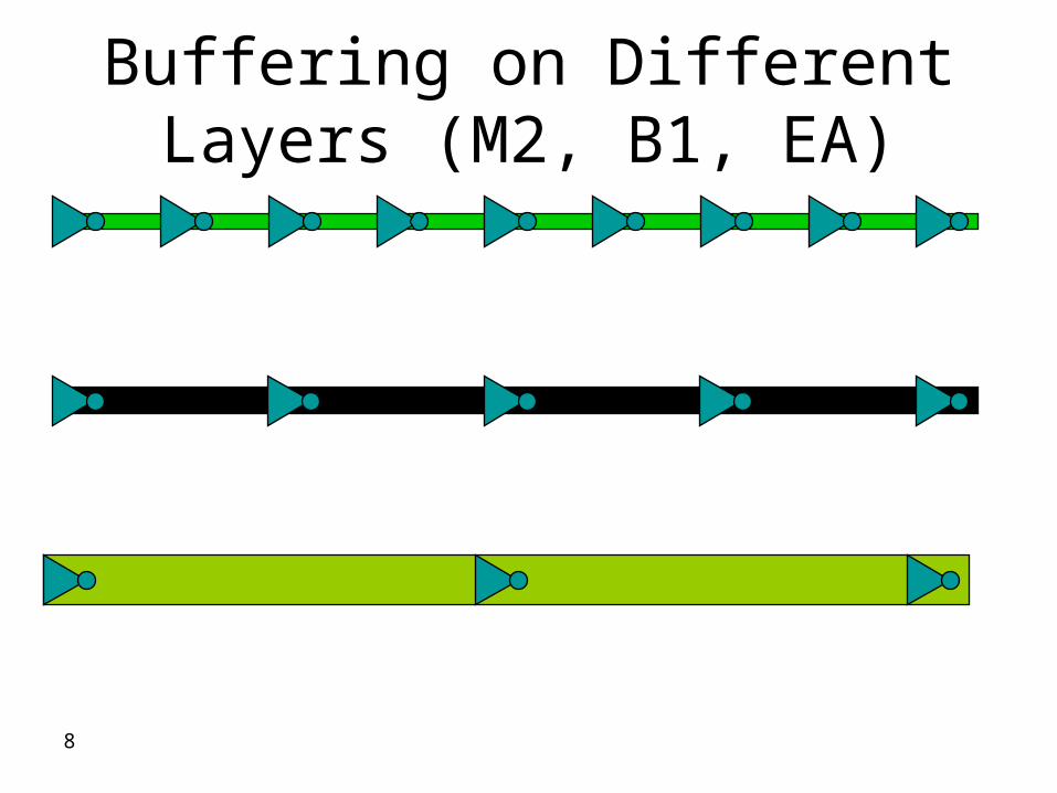
Buffering on Different Layers (M2 B1 EA)
9
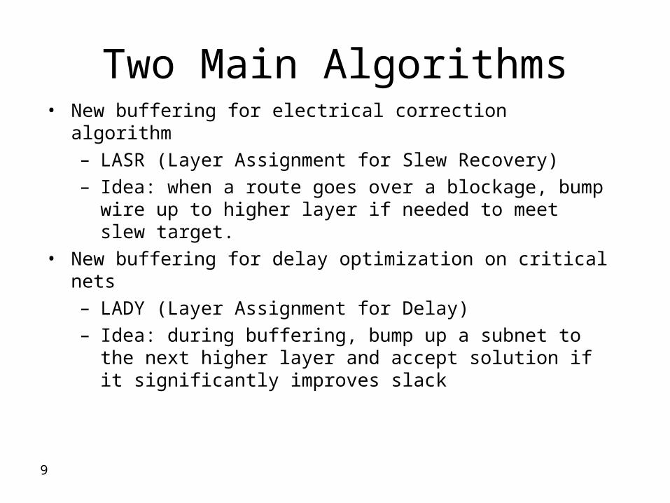
Two Main Algorithmsbull New buffering for electrical correction algorithm
ndash LASR (Layer Assignment for Slew Recovery)ndash Idea when a route goes over a blockage bump wire up to
higher layer if needed to meet slew targetbull New buffering for delay optimization on critical nets
ndash LADY (Layer Assignment for Delay)ndash Idea during buffering bump up a subnet to the next higher
layer and accept solution if it significantly improves slack
10
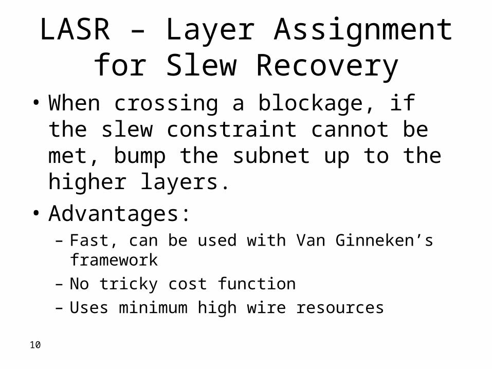
LASR ndash Layer Assignment for Slew Recovery
bull When crossing a blockage if the slew constraint cannot be met bump the subnet up to the higher layers
bull Advantagesndash Fast can be used with Van Ginnekenrsquos frameworkndash No tricky cost functionndash Uses minimum high wire resources
11
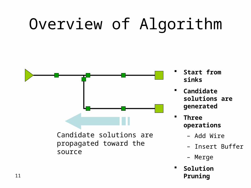
Overview of Algorithm
Candidate solutions are propagated toward the source
Start from sinks
Candidate solutions are generated
Three operations
ndash Add Wire
ndash Insert Buffer
ndash Merge
Solution Pruning
12
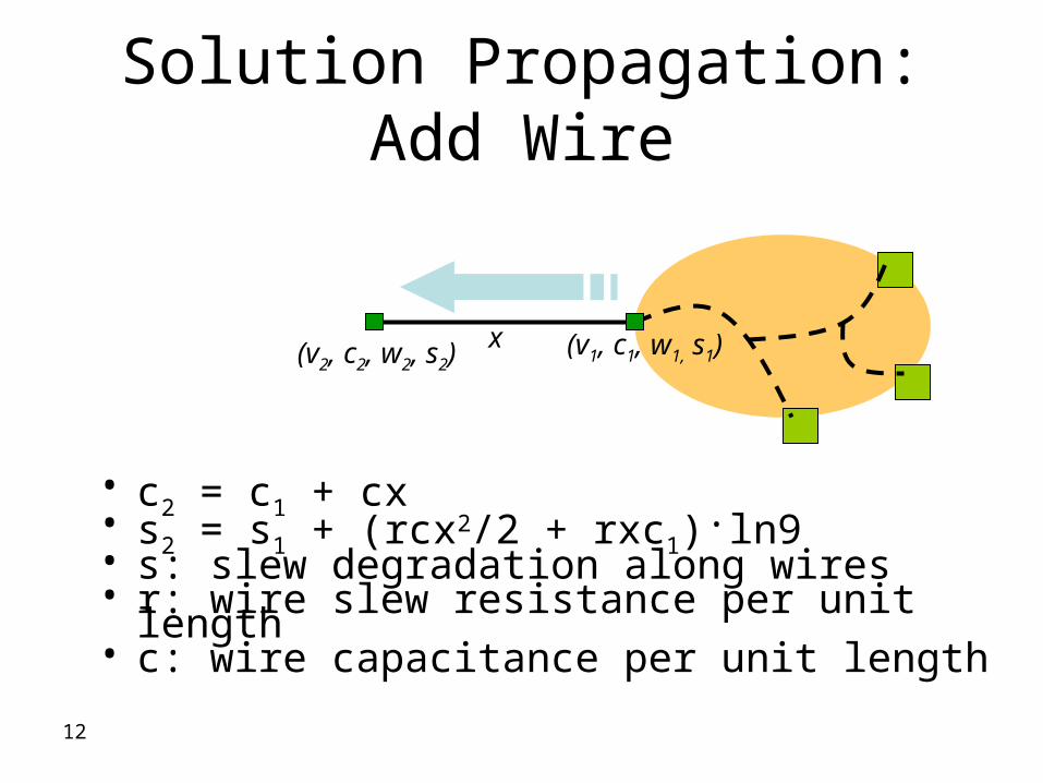
Solution Propagation Add Wire
bull c2 = c1 + cxbull s2 = s1 + (rcx22 + rxc1)ln9bull s slew degradation along wiresbull r wire slew resistance per unit lengthbull c wire capacitance per unit length
(v1 c1 w1 s1)
(v2 c2 w2 s2)
x
13
Solution Propagation Insert Buffer
c1b = Cb s1b = 0
w1b = w1+w(b)Cb buffer input capacitancePruned if the following slew constraint is violated
If no solution can satisfy the slew constraint bump the subnet to the next higher layer and compute the solution which satisfies the slew constraint and with minimum cost
(v1 c1 w1 s1)(v1 c1b w1b s1b)
14
Solution Propagation Merge
bull cmerge = cl + cr
bull wmerge = wl + wr
bull smerge = max(sl sr)
(v cl wl sl) (v cr wlrsr)
15
Solution Pruning
bull Two candidate solutionsndash Solution 1 (v c1 w1 s1)
ndash Solution 2 (v c2 w2 s2)
bull Solution 1 is inferior if ndash c1 gt c2 larger load
ndash and w1 gt w2 larger buffer area
ndash and s1 gt s2 worse cumulative slew degradation on wire
16
LASR Example
Slew constraint can not be met so bump up to the higher layer
Slew constraint still can not be met
17
LADY ndash Layer Assignment for Delay
bull Idea Use traditional Van Ginnekenrsquos algorithm but pick a fatter wire if it buys you X ps improvement
bull X is tunable parm eg 5-500 ps
bull Guarantees only long nets get promoted to thick metal
bull No complicated user-specified cost function
bull Small runtime overhead (5)
18
Solution Propagation Insert Buffer
c1b = Cb q1b = q1-RbC1
w1b = w1+w(b)Cb buffer input capacitanceRb buffer driving resistance
Bump the subnet to the next higher layer if it can obtain X ps improvement
(v1 c1 w1 q1)(v1 c1b w1b q1b)
19
LADY Example (X = 5 ps)
Delay 18 ps
Delay 10 ps
Delay 7 ps
Delay 50 ps
Delay 22 ps
Delay 14 ps
8 ps
3 ps
28 ps
8 ps
20
Experiment resultsbull Experiments on XPP Top in Cu65 technology (6 layers)
-400E+04-350E+04-300E+04-250E+04-200E+04-150E+04-100E+04-500E+03000E+00
FOM
Baseline WireOpt LADY+LASR
114E+06
116E+06
118E+06
120E+06
122E+06
124E+06W
irele
ngth
Baseline WireOpt LADY+LASR
-250E+00
-200E+00
-150E+00
-100E+00
-500E-01
000E+00
Wor
st S
lack
Baseline WireOpt LADY+LASR
315E+02
316E+02
317E+02
318E+02
319E+02
320E+02
321E+02
Area
Baseline WireOpt LADY+LASR
21
Observation
bull LADY+LASR improves (for the whole PDS)ndash FOM by 63ndash Worst Slack by 52ndash Area by 1ndash Wirelength by 4
22
Benefits
bull Two buffering techniques considering layer assignment LASR and LADY
bull LASR+LADY can obtainbull Over 50 slack improvement (for worst slack and
total slack)bull 1 reduction in area and 4 reduction in
wirelength
Bus design
bull Bundles of signals treated symmetricallyndash Identical electricalphysical environment for each bitndash Need to consider synchronization
bull Abstraction of communication during early designndash Often integrated with floorplanning ndash Global busses often pre-designed prior to detailed block
implementation (esp in microprocessors)
Congestion considerations
bull Designs increasingly wire-limitedbull Interconnect optimization routing resource intensive
ndash spacing wide-wires up-layeringbull Congestion can cause detours (or even unroutable designs)bull Detours increase interconnect delay as well as
interconnect delay unpredictabilityndash Wire delay models during tech-mapping placement are based
on shortest path routingndash Detours increase convergence problems because of poor
upstream wire delay modeling
Referencesbull J Cong and L He ldquoTheory and algorithm of local refinement based optimization with
application to device and interconnect sizingrdquo IEEE Trans CAD pp 406-420 Apr 1999
bull J Cong ldquoAn interconnect-centric design flow for nanometer technologiesrdquo Proc IEEE pp 505-528 April 2001
bull J Lillis C-K Cheng T-T Lin and C-Y Ho ldquoNew performance-driven routing techniques with explicit areadelay tradeoff and simultaneous wire sizingrdquo Proc DAC pp 395-400 June 1996
bull M Hrkic and J Lillis ldquoS-tree A technique for buffered routing tree synthesisrdquo Proc DAC pp 98-103 June 2002
bull L van Ginneken ldquoBuffer placement in distributed RC-tree networks for minimal Elmore delayrdquo Proc ISCAS pp 865-868 1990
bull C Alpert M Hrkic J Hu and S Quay ldquoFast and flexible buffer trees that navigate the physical layout environmentrdquo Proc DAC pp 24-29 June 2004
bull M Becer R Vaidyanathan C Oh and R Panda ldquoCrosstalk noise control in an SoC physical design flowrdquo IEEE Trans CAD pp 488-497 Apr 2004
Buffering Related Interconnect Synthesis
bull Considerndash Layer assignmentndash Wire sizingndash Buffer polarityndash Driver sizingndash Generalized bufferingndash Blockagesndash Wire segmentingndash Higher order delay modelsndash Noisendash Bus designndash Buffer libraryndash Simultaneous routing and bufferingndash Simultaneous gate sizing and buffering
3
Layer assignment
bull With advancing technology buffering considering layer assignment becomes increasingly important
bull Wire in higher layer has smaller delay Thus a buffer can drive longer distances in higher layers
bull Timing timing is improved
bull Area cost Fewer buffers needed
bull Experiments demonstrate that one can achieve
bull Over 50 slack improvement (for worst slack and total slack)
bull 1 reduction in area and 4 reduction in wirelength
4
Layer Assignment Problem for cu65
1X
2X
4X
5
An Awakening in the Designer Community
IP
IP0
10
20
30
40
50
60
70
80
90
01 02 03 04 05 06 07
wire length
wir
e d
elay M2
B1
EA
6
Cu65HP Metal RC Characteristics
000E+00
500E-01
100E+00
150E+00
200E+00
Res
ista
nce
M3 B1 EA
000E+00
500E+01
100E+02
150E+02
200E+02
250E+02
Capaci
tance
M3 B1 EA
7
Expected distances between Buffers for cu65
bull Created a very long 2-pin net for cu65bull Ran buffopt using each buffer from the library in turn
1x 2x 4x
Spacing (mm)
Delay BufferSpacing
(mm)Delay Buffer
Spacing (mm)
Delay buffer
05 slew target
094BUFX11BA12TR
199BUFX16BA12TR
342INVX16BA12TR
07 slew target
112INVX4BA
12TR 233
INVX9A12TR
418INVX16A
12TR
10 slew target
137INVX4BA
12TR 288
INVX7P5BA12TR
512BUFX16A12TR
optimum delay
070 135BUFX13A12PTR
149 69BUFX16A12PTR
268 45BUFX16A12PTR
1 A buffer can drive longer (2x-35x) distance in higher layers with better delay
2 Fewer buffers needed
8
Buffering on Different Layers (M2 B1 EA)
9
Two Main Algorithmsbull New buffering for electrical correction algorithm
ndash LASR (Layer Assignment for Slew Recovery)ndash Idea when a route goes over a blockage bump wire up to
higher layer if needed to meet slew targetbull New buffering for delay optimization on critical nets
ndash LADY (Layer Assignment for Delay)ndash Idea during buffering bump up a subnet to the next higher
layer and accept solution if it significantly improves slack
10
LASR ndash Layer Assignment for Slew Recovery
bull When crossing a blockage if the slew constraint cannot be met bump the subnet up to the higher layers
bull Advantagesndash Fast can be used with Van Ginnekenrsquos frameworkndash No tricky cost functionndash Uses minimum high wire resources
11
Overview of Algorithm
Candidate solutions are propagated toward the source
Start from sinks
Candidate solutions are generated
Three operations
ndash Add Wire
ndash Insert Buffer
ndash Merge
Solution Pruning
12
Solution Propagation Add Wire
bull c2 = c1 + cxbull s2 = s1 + (rcx22 + rxc1)ln9bull s slew degradation along wiresbull r wire slew resistance per unit lengthbull c wire capacitance per unit length
(v1 c1 w1 s1)
(v2 c2 w2 s2)
x
13
Solution Propagation Insert Buffer
c1b = Cb s1b = 0
w1b = w1+w(b)Cb buffer input capacitancePruned if the following slew constraint is violated
If no solution can satisfy the slew constraint bump the subnet to the next higher layer and compute the solution which satisfies the slew constraint and with minimum cost
(v1 c1 w1 s1)(v1 c1b w1b s1b)
14
Solution Propagation Merge
bull cmerge = cl + cr
bull wmerge = wl + wr
bull smerge = max(sl sr)
(v cl wl sl) (v cr wlrsr)
15
Solution Pruning
bull Two candidate solutionsndash Solution 1 (v c1 w1 s1)
ndash Solution 2 (v c2 w2 s2)
bull Solution 1 is inferior if ndash c1 gt c2 larger load
ndash and w1 gt w2 larger buffer area
ndash and s1 gt s2 worse cumulative slew degradation on wire
16
LASR Example
Slew constraint can not be met so bump up to the higher layer
Slew constraint still can not be met
17
LADY ndash Layer Assignment for Delay
bull Idea Use traditional Van Ginnekenrsquos algorithm but pick a fatter wire if it buys you X ps improvement
bull X is tunable parm eg 5-500 ps
bull Guarantees only long nets get promoted to thick metal
bull No complicated user-specified cost function
bull Small runtime overhead (5)
18
Solution Propagation Insert Buffer
c1b = Cb q1b = q1-RbC1
w1b = w1+w(b)Cb buffer input capacitanceRb buffer driving resistance
Bump the subnet to the next higher layer if it can obtain X ps improvement
(v1 c1 w1 q1)(v1 c1b w1b q1b)
19
LADY Example (X = 5 ps)
Delay 18 ps
Delay 10 ps
Delay 7 ps
Delay 50 ps
Delay 22 ps
Delay 14 ps
8 ps
3 ps
28 ps
8 ps
20
Experiment resultsbull Experiments on XPP Top in Cu65 technology (6 layers)
-400E+04-350E+04-300E+04-250E+04-200E+04-150E+04-100E+04-500E+03000E+00
FOM
Baseline WireOpt LADY+LASR
114E+06
116E+06
118E+06
120E+06
122E+06
124E+06W
irele
ngth
Baseline WireOpt LADY+LASR
-250E+00
-200E+00
-150E+00
-100E+00
-500E-01
000E+00
Wor
st S
lack
Baseline WireOpt LADY+LASR
315E+02
316E+02
317E+02
318E+02
319E+02
320E+02
321E+02
Area
Baseline WireOpt LADY+LASR
21
Observation
bull LADY+LASR improves (for the whole PDS)ndash FOM by 63ndash Worst Slack by 52ndash Area by 1ndash Wirelength by 4
22
Benefits
bull Two buffering techniques considering layer assignment LASR and LADY
bull LASR+LADY can obtainbull Over 50 slack improvement (for worst slack and
total slack)bull 1 reduction in area and 4 reduction in
wirelength
Bus design
bull Bundles of signals treated symmetricallyndash Identical electricalphysical environment for each bitndash Need to consider synchronization
bull Abstraction of communication during early designndash Often integrated with floorplanning ndash Global busses often pre-designed prior to detailed block
implementation (esp in microprocessors)
Congestion considerations
bull Designs increasingly wire-limitedbull Interconnect optimization routing resource intensive
ndash spacing wide-wires up-layeringbull Congestion can cause detours (or even unroutable designs)bull Detours increase interconnect delay as well as
interconnect delay unpredictabilityndash Wire delay models during tech-mapping placement are based
on shortest path routingndash Detours increase convergence problems because of poor
upstream wire delay modeling
Referencesbull J Cong and L He ldquoTheory and algorithm of local refinement based optimization with
application to device and interconnect sizingrdquo IEEE Trans CAD pp 406-420 Apr 1999
bull J Cong ldquoAn interconnect-centric design flow for nanometer technologiesrdquo Proc IEEE pp 505-528 April 2001
bull J Lillis C-K Cheng T-T Lin and C-Y Ho ldquoNew performance-driven routing techniques with explicit areadelay tradeoff and simultaneous wire sizingrdquo Proc DAC pp 395-400 June 1996
bull M Hrkic and J Lillis ldquoS-tree A technique for buffered routing tree synthesisrdquo Proc DAC pp 98-103 June 2002
bull L van Ginneken ldquoBuffer placement in distributed RC-tree networks for minimal Elmore delayrdquo Proc ISCAS pp 865-868 1990
bull C Alpert M Hrkic J Hu and S Quay ldquoFast and flexible buffer trees that navigate the physical layout environmentrdquo Proc DAC pp 24-29 June 2004
bull M Becer R Vaidyanathan C Oh and R Panda ldquoCrosstalk noise control in an SoC physical design flowrdquo IEEE Trans CAD pp 488-497 Apr 2004
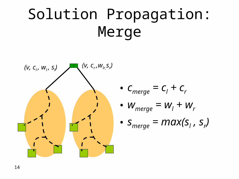
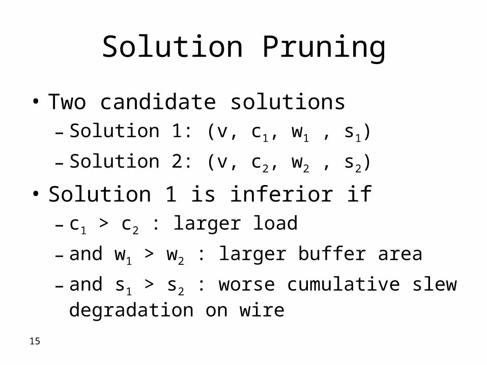
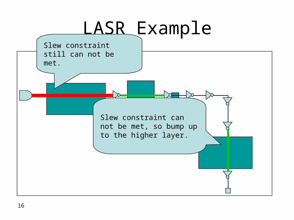
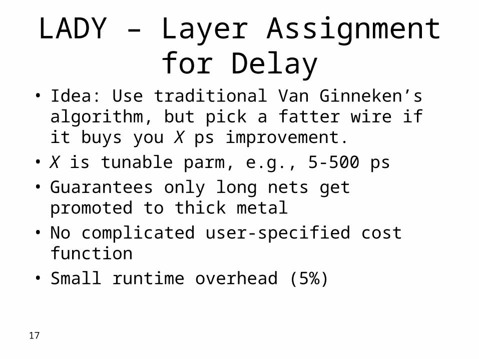
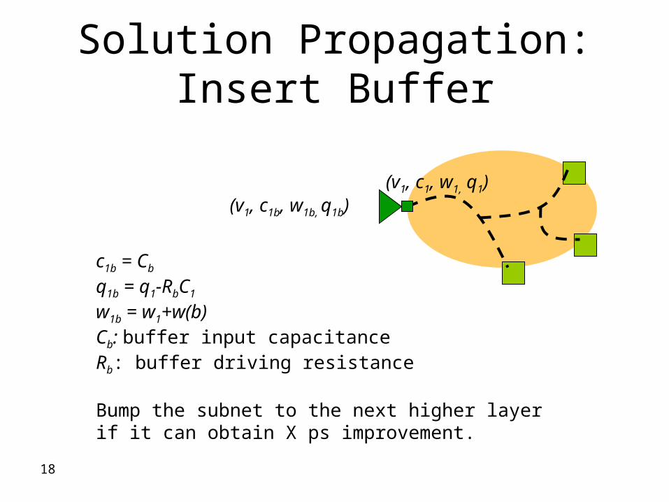
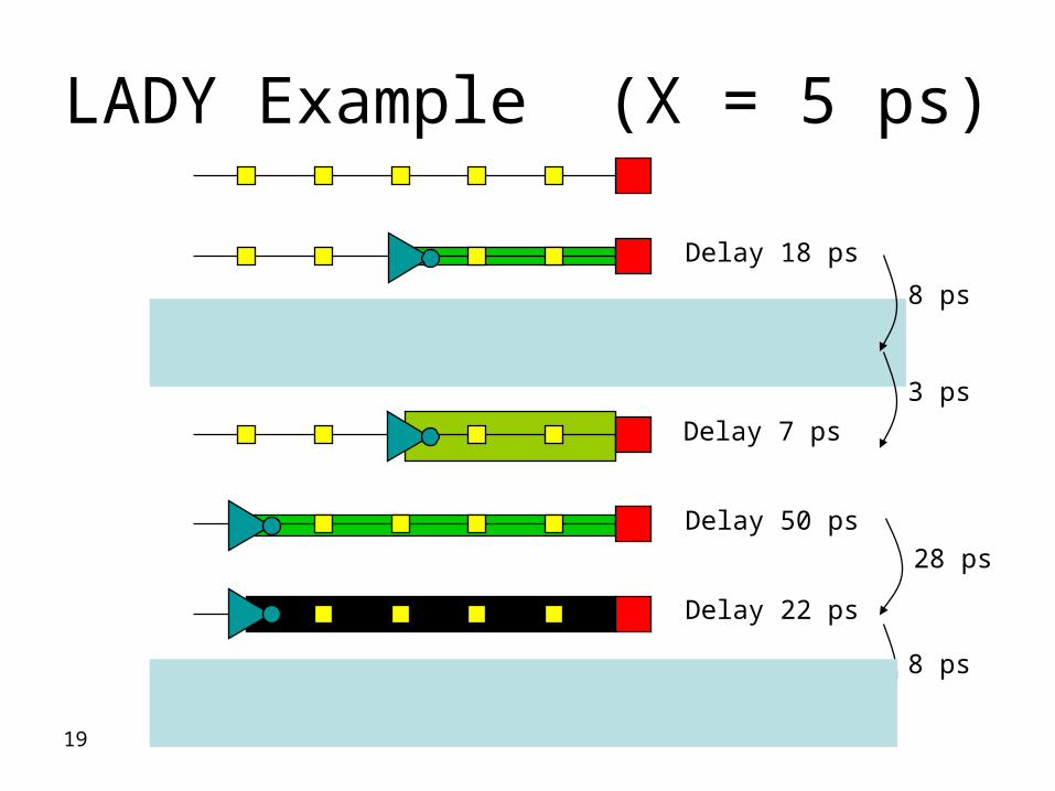
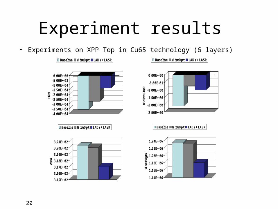
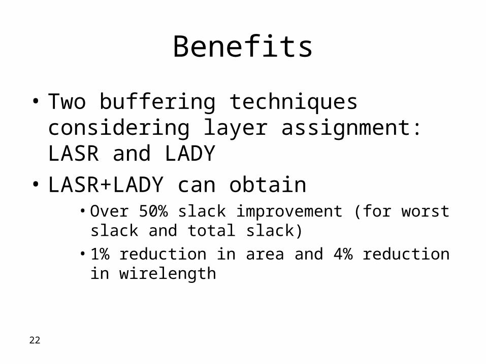
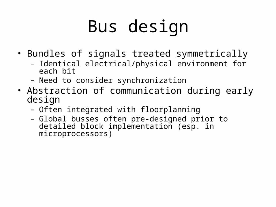
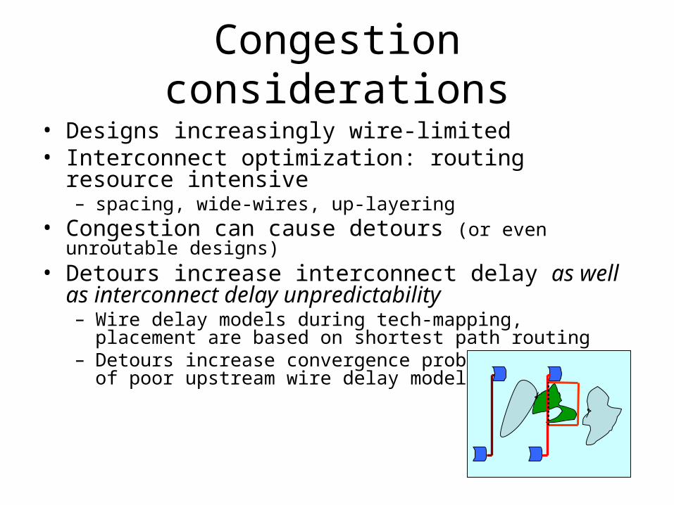
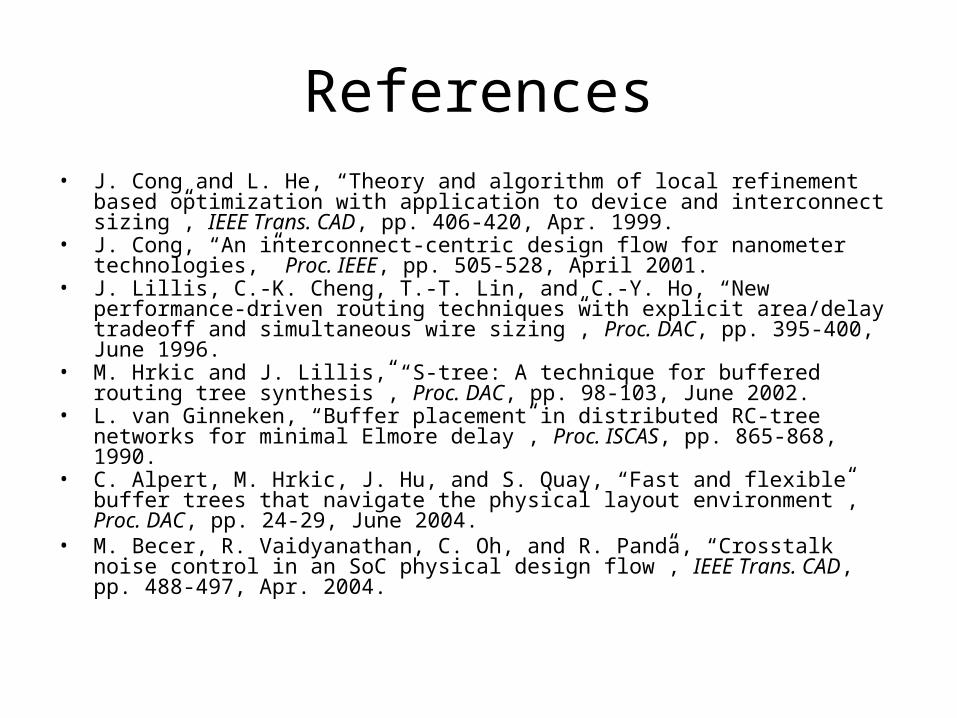


