Interface Structure of Cu Wire Bonding on Cu Substrate with Sn Plating
Shinichi Fujiwara1,+ and Reinhold H. Dauskardt2
1Yokohama Research Laboratory, Hitachi, Ltd., Yokohama 244-0817, Japan2Stanford University, Stanford, CA 94305-4034, USA
In previous research on copper wire bonding on a copper substrate with tin plating, suitable thickness and binding conditions for the tinplating were chosen using the peel test after the copper wire bonding. These conditions were determined to be a thickness of 10 microns, a stagetemperature of 373K, a bonding power of 500 to 700mW and a bonding time of 30 to 50ms. Cross-sectional observations of the bondinginterface indicated that the tin layer remained between the copper wire and copper substrate after bonding under these conditions. The purpose ofthe present study was to evaluate the joint interface structure of the bonded copper wire on the copper substrate with the tin plating. Residual Snexists locally at the initial bonding interface, and the locations bonded to the interstitial Sn are intermixed with the locations where the Cu wire isbonded to a CuSn intermetallic compound. No oxide film layer was found at the bonding interface in the joint between the Cu wire and CuSnintermetallic compound; TEM images indicated that these have metallic bonding in which Cu and Cu3Sn are directly bonded. This is in contrastto ultrasonic bonding between Cu and Sn, wherein the Cu and Sn are bonded by means of the Sn oxide film.[doi:10.2320/matertrans.MB201203]
(Received June 1, 2012; Accepted August 16, 2012; Published November 25, 2012)
Wire bonding has long been used for connecting theelectrodes of semiconductor devices to external terminals,and currently remains the mainstream method for thispurpose. Gold (Au) wires are most often used becausethey are easy to work with and exhibit superior corrosionresistance; they have been extensively investigated.1,2)
Meanwhile, pad pitches continue to decrease and by 2018,the minimum pad pitch is expected to be 30 µm andthe minimum wire diameter 12.5 µm.3) However, becausebonding reliability decreases when Au reacts with the Al usedfor wiring in semiconductor devices,4) and neck breaks canoccur, increasing cost, as wire diameters become finer.Thus selecting a material to replace Au is a crucial problem.Ag, Al and Cu are being studied as a replacement for Au;58)
of these, Cu is probably the strongest candidate for futurefiner pitch applications due to its superior thermal andelectrical conductivity, and its strength against neck breaks.However, Cu is difficult to form into uniform balls for ballbonding since it readily forms an oxide film in air. Cu alsorequires greater power during bonding since it is moredifficult to deform compared to Au.
In the current research, we conducted a study of wedgebonding wherein wires are directly bonded without forminga Cu ball. In addition, Cu, which is widely used as thewiring material for substrates and leads, was selected as thematerial for the electrodes and external terminals to whichthe Cu wire was bonded, and the bondability of Cu wireto Cu substrates was evaluated. Cu wire bonding to Cusubstrates has been previously studied; however surfaceoxidation of Cu remains a concern.911) In previousinvestigations,12) the Cu wires were bonded after suppressingthe formation of oxide films on Cu by Sn-plating the Cusubstrate, and parameters for bonding the Cu wire to theCu substrate but leaving residual Sn at the joint interfacewere derived. In this study, the joint cross sections were
examined in detail by scanning electron microscopy (SEM)and transmission electron microscopy (TEM) to understandthe bonding state after initial bonding.
2. Experimental Procedure
2.1 Initial bonding test and bonding stateA manual wire ultrasonic bonding device was used in this
research. The ultrasound frequency was 63 kHz, the bondingload range was 0.17 to 0.88N, and the bonding power andultrasound application time were arbitrarily set. The Cu wireused in this research had 99.99% purity, showed 8 to 16%elongation, and 0.12N breaking load. The wire diameterwas 25 µm.
A Cu substrate, C1020R type, with 10-µm-thick Sn platingwas secured on a hotplate with the Sn-plated side up. Cu wirebonding was performed after cleaning the Sn-plated surfacewith alcohol. The bonding load was fixed at 0.5N, and thetemperature of the hotplate was set to 373K for 60 s. TheSn-plated Cu substrate used in this work formed a CuSnintermetallic compound before bonding.
Previous research suggested that good bonding could beachieved by heating a Cu substrate with a 10-µm-thick Snplating to 373K at a bonding power of 500 to 700mW for 30to 50ms.12) The joint strength was found to be approximately0.05N. From this result, the initial bonding state and long-term reliability were evaluated for bonding at 500mW for30ms, which allowed high joint strength to be achieved ina short time.
Wire surface conditions were observed by SEM from a 52degree tilted view of the bonded wire. The bonding stateswere subsequently observed using focused ion beam (FIB)milling to prepare a cross section in the vertical directionrelative to the bonding surface.
2.2 TEM observation of the Cu wire/Sn/Cu bondinginterfaces
A Hitachi FIB milling system and a dual beam FIB/SEM(FEI) system were used to prepare TEM samples. A field+Corresponding author, E-mail: [email protected]
emission transmission electron microscope (JEOL Ltd.) wasused for the TEM observations at an acceleration voltage of200 kV. Thin film samples of the Cu wire/Sn plating/Cusubstrate joint face were prepared by FIB for TEM. Electronbeam diameter of TEM analysis is 1nm.
3. Results and Discussion
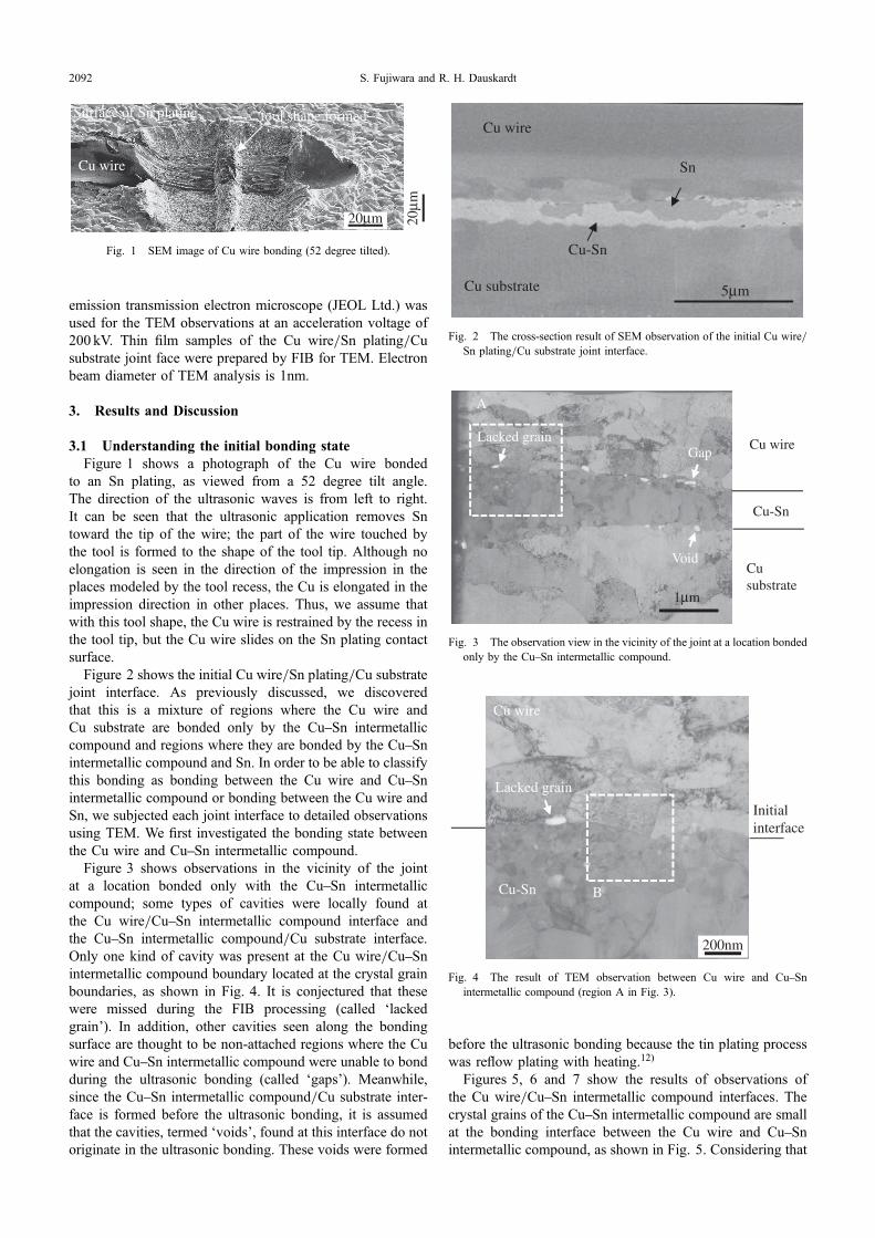
3.1 Understanding the initial bonding stateFigure 1 shows a photograph of the Cu wire bonded
to an Sn plating, as viewed from a 52 degree tilt angle.The direction of the ultrasonic waves is from left to right.It can be seen that the ultrasonic application removes Sntoward the tip of the wire; the part of the wire touched bythe tool is formed to the shape of the tool tip. Although noelongation is seen in the direction of the impression in theplaces modeled by the tool recess, the Cu is elongated in theimpression direction in other places. Thus, we assume thatwith this tool shape, the Cu wire is restrained by the recess inthe tool tip, but the Cu wire slides on the Sn plating contactsurface.
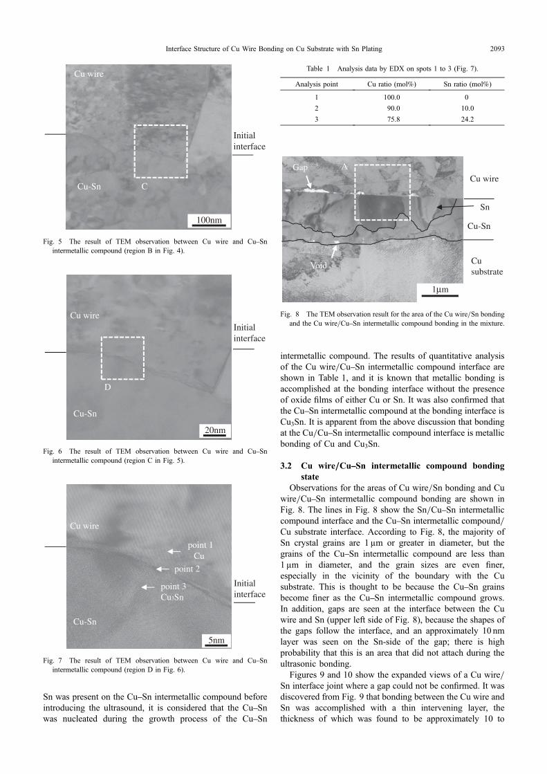
Figure 2 shows the initial Cu wire/Sn plating/Cu substratejoint interface. As previously discussed, we discoveredthat this is a mixture of regions where the Cu wire andCu substrate are bonded only by the CuSn intermetalliccompound and regions where they are bonded by the CuSnintermetallic compound and Sn. In order to be able to classifythis bonding as bonding between the Cu wire and CuSnintermetallic compound or bonding between the Cu wire andSn, we subjected each joint interface to detailed observationsusing TEM. We first investigated the bonding state betweenthe Cu wire and CuSn intermetallic compound.
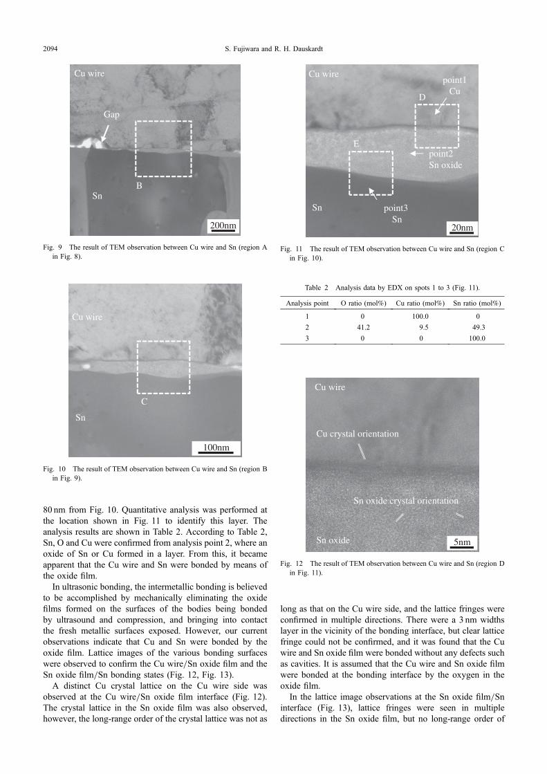
Figure 3 shows observations in the vicinity of the jointat a location bonded only with the CuSn intermetalliccompound; some types of cavities were locally found atthe Cu wire/CuSn intermetallic compound interface andthe CuSn intermetallic compound/Cu substrate interface.Only one kind of cavity was present at the Cu wire/CuSnintermetallic compound boundary located at the crystal grainboundaries, as shown in Fig. 4. It is conjectured that thesewere missed during the FIB processing (called ‘lackedgrain’). In addition, other cavities seen along the bondingsurface are thought to be non-attached regions where the Cuwire and CuSn intermetallic compound were unable to bondduring the ultrasonic bonding (called ‘gaps’). Meanwhile,since the CuSn intermetallic compound/Cu substrate inter-face is formed before the ultrasonic bonding, it is assumedthat the cavities, termed ‘voids’, found at this interface do notoriginate in the ultrasonic bonding. These voids were formed
before the ultrasonic bonding because the tin plating processwas reflow plating with heating.12)
Figures 5, 6 and 7 show the results of observations ofthe Cu wire/CuSn intermetallic compound interfaces. Thecrystal grains of the CuSn intermetallic compound are smallat the bonding interface between the Cu wire and CuSnintermetallic compound, as shown in Fig. 5. Considering that
20µm
Surface of Sn plating
Cu wire
tool shape formed
20µm
Fig. 1 SEM image of Cu wire bonding (52 degree tilted).
5µm
Sn
Cu-Sn
Cu substrate
Cu wire
Fig. 2 The cross-section result of SEM observation of the initial Cu wire/Sn plating/Cu substrate joint interface.
A
Cu wire
Cu-Sn
Cu substrate
1µm
Lacked grainGap
Void
Fig. 3 The observation view in the vicinity of the joint at a location bondedonly by the CuSn intermetallic compound.
B
Cu wire
Cu-Sn
Initial interface
200nm
Lacked grain
Fig. 4 The result of TEM observation between Cu wire and CuSnintermetallic compound (region A in Fig. 3).
S. Fujiwara and R. H. Dauskardt2092
Sn was present on the CuSn intermetallic compound beforeintroducing the ultrasound, it is considered that the CuSnwas nucleated during the growth process of the CuSn
intermetallic compound. The results of quantitative analysisof the Cu wire/CuSn intermetallic compound interface areshown in Table 1, and it is known that metallic bonding isaccomplished at the bonding interface without the presenceof oxide films of either Cu or Sn. It was also confirmed thatthe CuSn intermetallic compound at the bonding interface isCu3Sn. It is apparent from the above discussion that bondingat the Cu/CuSn intermetallic compound interface is metallicbonding of Cu and Cu3Sn.
3.2 Cu wire/CuSn intermetallic compound bondingstate
Observations for the areas of Cu wire/Sn bonding and Cuwire/CuSn intermetallic compound bonding are shown inFig. 8. The lines in Fig. 8 show the Sn/CuSn intermetalliccompound interface and the CuSn intermetallic compound/Cu substrate interface. According to Fig. 8, the majority ofSn crystal grains are 1 µm or greater in diameter, but thegrains of the CuSn intermetallic compound are less than1 µm in diameter, and the grain sizes are even finer,especially in the vicinity of the boundary with the Cusubstrate. This is thought to be because the CuSn grainsbecome finer as the CuSn intermetallic compound grows.In addition, gaps are seen at the interface between the Cuwire and Sn (upper left side of Fig. 8), because the shapes ofthe gaps follow the interface, and an approximately 10 nmlayer was seen on the Sn-side of the gap; there is highprobability that this is an area that did not attach during theultrasonic bonding.
Figures 9 and 10 show the expanded views of a Cu wire/Sn interface joint where a gap could not be confirmed. It wasdiscovered from Fig. 9 that bonding between the Cu wire andSn was accomplished with a thin intervening layer, thethickness of which was found to be approximately 10 to
Initial interface
C
Cu wire
Cu-Sn
100nm
Fig. 5 The result of TEM observation between Cu wire and CuSnintermetallic compound (region B in Fig. 4).
Initial interface
D
Cu wire
Cu-Sn
20nm
Fig. 6 The result of TEM observation between Cu wire and CuSnintermetallic compound (region C in Fig. 5).
Initial interface
point 1Cu
point 2
point 3Cu3Sn
Cu wire
Cu-Sn
5nm
Fig. 7 The result of TEM observation between Cu wire and CuSnintermetallic compound (region D in Fig. 6).
Table 1 Analysis data by EDX on spots 1 to 3 (Fig. 7).
Analysis point Cu ratio (mol%) Sn ratio (mol%)
1 100.0 0
2 90.0 10.0
3 75.8 24.2
ACu wire
Cu-Sn
Sn
Cu substrate
1µm
Gap
Void
Fig. 8 The TEM observation result for the area of the Cu wire/Sn bondingand the Cu wire/CuSn intermetallic compound bonding in the mixture.
Interface Structure of Cu Wire Bonding on Cu Substrate with Sn Plating 2093
80 nm from Fig. 10. Quantitative analysis was performed atthe location shown in Fig. 11 to identify this layer. Theanalysis results are shown in Table 2. According to Table 2,Sn, O and Cu were confirmed from analysis point 2, where anoxide of Sn or Cu formed in a layer. From this, it becameapparent that the Cu wire and Sn were bonded by means ofthe oxide film.
In ultrasonic bonding, the intermetallic bonding is believedto be accomplished by mechanically eliminating the oxidefilms formed on the surfaces of the bodies being bondedby ultrasound and compression, and bringing into contactthe fresh metallic surfaces exposed. However, our currentobservations indicate that Cu and Sn were bonded by theoxide film. Lattice images of the various bonding surfaceswere observed to confirm the Cu wire/Sn oxide film and theSn oxide film/Sn bonding states (Fig. 12, Fig. 13).
A distinct Cu crystal lattice on the Cu wire side wasobserved at the Cu wire/Sn oxide film interface (Fig. 12).The crystal lattice in the Sn oxide film was also observed,however, the long-range order of the crystal lattice was not as
long as that on the Cu wire side, and the lattice fringes wereconfirmed in multiple directions. There were a 3 nm widthslayer in the vicinity of the bonding interface, but clear latticefringe could not be confirmed, and it was found that the Cuwire and Sn oxide film were bonded without any defects suchas cavities. It is assumed that the Cu wire and Sn oxide filmwere bonded at the bonding interface by the oxygen in theoxide film.
In the lattice image observations at the Sn oxide film/Sninterface (Fig. 13), lattice fringes were seen in multipledirections in the Sn oxide film, but no long-range order of
B
Cu wire
Sn
Gap
200nm
Fig. 9 The result of TEM observation between Cu wire and Sn (region Ain Fig. 8).
C
Cu wire
Sn
100nm
Fig. 10 The result of TEM observation between Cu wire and Sn (region Bin Fig. 9).
point2Sn oxide
point3Sn
D
E
Cu wire
Sn
point1Cu
20nm
Fig. 11 The result of TEM observation between Cu wire and Sn (region Cin Fig. 10).
Table 2 Analysis data by EDX on spots 1 to 3 (Fig. 11).
Analysis point O ratio (mol%) Cu ratio (mol%) Sn ratio (mol%)
1 0 100.0 0
2 41.2 9.5 49.3
3 0 0 100.0
Cu wire
Sn oxide crystal orientation
Sn oxide
Cu crystal orientation
5nm
Fig. 12 The result of TEM observation between Cu wire and Sn (region Din Fig. 11).
S. Fujiwara and R. H. Dauskardt2094
any kind was observed. However, a Sn crystal lattice couldbe distinctly confirmed on the Sn side, and continuity wasfound to be high. In addition, unlike in the interface betweenthe Cu wire and the Sn oxide film, no areas of contrast couldbe confirmed, nor were any cavities found in the vicinity ofthe interface. This is thought to be due to the differencesin the bonding mechanism between the Sn oxide film andSn and the bonding mechanism between the Cu wire andSn oxide film. This Sn oxide film was formed by leavingthe Sn exposed to air in the sample preparation process.Therefore, we assume that bonding at the interface betweenthe Sn oxide film and the Sn as seen in Fig. 13 is dueto bonding by oxygen, as in common metal oxide films.In addition, since this interface is formed without addingany external energy, it is thought that the Sn oxide film/Sninterface can also be distinctly confirmed. However, weassume that the areas of contrast were formed by forcedbonding, since the interface between the Cu wire and Snoxide film was formed by the ultrasound energy andcompression during bonding.
In this investigation, we thus discovered that metals andoxide films could be locally bonded by ultrasonic bonding ofCu wire and Sn oxide film.
3.3 Bonding state at Cu wire/Sn interfaceFigure 14 shows SEM observation of the joint cross-
section after peel testing of the Cu wires bonded at 500mWfor 30ms. This joint is the remaining joint at one end ofa wire that was subjected to a peel test at 0.05N, the otherjoint having been ruptured. From Fig. 14, it can be seenthat though there were local Sn regions, the Cu wire wasbonded to a CuSn intermetallic compound. In addition,voids were seen at the interface between the CuSnintermetallic compound and the Cu substrate, and cracksthat developed in the peel test had advanced into the interfacebetween the CuSn intermetallic compound and Cu wire orinto the Sn.
Consequently, we were able to confirm that for Cu wirebonded to the Sn-plated Cu under these bonding conditions,residual Sn was locally present at the bonding interface
between the wire and Cu substrate, and bonding took placebetween the wire and the CuSn intermetallic compound.
4. Conclusion
The following conclusions were obtained with regard tothe Cu wire bonding to a Sn-plated Cu substrate.(1) Residual Sn exists locally at the initial bonding
interface, and the locations bonded with interstitial Snare intermixed with locations where the Cu wire isbonded with the CuSn intermetallic compound.
(2) No oxide film layer was found at the bonding interfacein the joint between the Cu wire and the CuSnintermetallic compound, which TEM lattice imagesshowed to be metallic bonding with Cu and Cu3Snbeing directly bonded.
(3) At locations where there was residual Sn, the Cu wireand Sn were bonded with an interstitial Sn oxide film,and there was a bonding area of indistinct crystalorientation of approximately 3 nm at the interfacebetween the Cu wire and Sn oxide film.
(4) In ultrasonic bonding between Cu and Sn, the bondingwas formed by the Sn oxide film.
Acknowledgments
The authors wish to thank Dr. M. S. Oliver, Dr. A. W.Hsing and Dr. T. S. Kim of Stanford University for theirsupport in making specimens.
REFERENCES
1) D. Y. Shinand and P. J. Ficalora: IEEE Trans. Electron. Dev. 26 (1979)2734.
2) S. Y. Yang, H. J. Byun, S. W. Park and W. J. Lee: Proc. 45th Annual onIEEE Reliability Physics Symposium, (2007) pp. 113116.
Sn oxide
Sn
Sn crystal orientation
Sn oxidecrystal orientation
5nm
Fig. 13 The result of TEM observation between Cu wire and Sn (region Ein Fig. 11).
Cu wire
Cu-Sn
Cu substrate
Crack by peel testing
Sn
Void
1µm
1µm
Fig. 14 The result of SEM observation of the joint cross section after peeltesting of Cu wires bonded at 500mW for 30ms (52 degee tilted).
Interface Structure of Cu Wire Bonding on Cu Substrate with Sn Plating 2095
3) H. S. Chang, K. C. Hsieh, T. Martens and A. Yang: IEEE Trans.Compon. Packag. Tech. 27 (2004) 155160.
4) K. Toyozawa, K. Fujita, S. Minamide and T. Maeda: IEEE Trans.Compon. Hybrids Manuf. Tech. 13 (1990) 667672.
5) J. Schwizer, M. Mayer, D. Bolliger, O. Paul and H. Baltes: The 24thIEEE/CPMT Symposium on Electronics Manufacturing TechnologySymposium, (Austin, USA, 1999) pp. 108114.
6) S. Koyama, M. Takahashi and K. Ikeuchi: Solid State Ion. 172 (2004)397401.
7) M. Onishi and H. Fujibuchi: Trans. Jpn. Inst. Met. 16 (1975) 539548.
8) I. Shohji, T. Sakurai and S. Arai: Key Eng. Mater. 297300 (2005)28192824.
9) H. Xu, C. Liu, V. V. Silberschmidt and H. Wang: The 58th ElectronicComponents and Technology Conference, (Florida, USA, 2008)pp. 14241430.
10) H. Clauberg, B. Chylak, N. Wong, J. Yeung and E. Milke: IEEE CPMTSymposium Japan, (Tokyo, Japan, 2010) pp. 14.
11) M. Maeda, T. Sato, N. Inoue, D. Yagi and Y. Takahashi: Microelectron.Reliab. 51 (2011) 130136.
12) S. Fujiwara and R. H. Dauskardt: Q. J. Japan Weld. Soc. 28 (2010)362368.