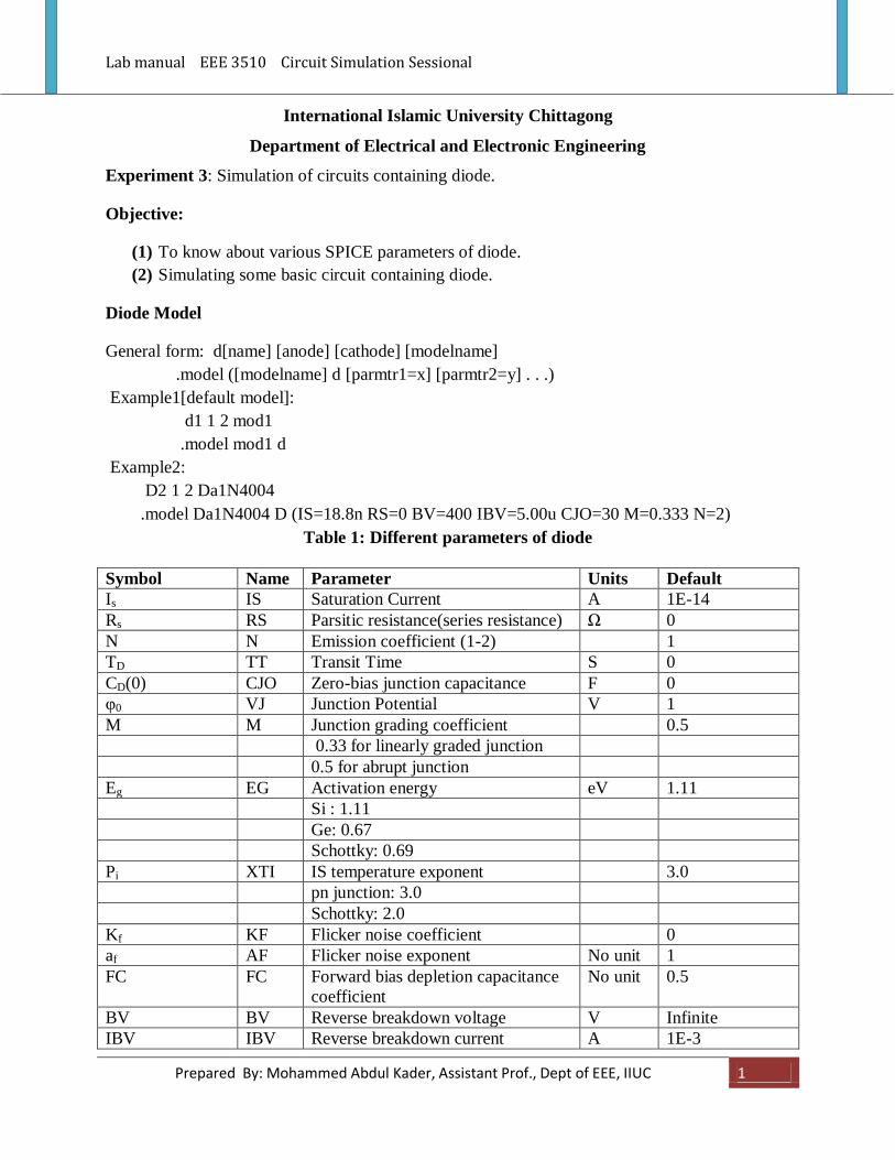
Lab manual EEE 3510 Circuit Simulation Sessional Prepared By: Mohammed Abdul Kader, Assistant Prof., Dept of EEE, IIUC 1 International Islamic University Chittagong Department of Electrical and Electronic Engineering Experiment 3: Simulation of circuits containing diode. Objective: (1) To know about various SPICE parameters of diode. (2) Simulating some basic circuit containing diode. Diode Model General form: d[name] [anode] [cathode] [modelname] .model ([modelname] d [parmtr1=x] [parmtr2=y] . . .) Example1[default model]: d1 1 2 mod1 .model mod1 d Example2: D2 1 2 Da1N4004 .model Da1N4004 D (IS=18.8n RS=0 BV=400 IBV=5.00u CJO=30 M=0.333 N=2) Table 1: Different parameters of diode Symbol Name Parameter Units Default I s IS Saturation Current A 1E-14 R s RS Parsitic resistance(series resistance) Ω 0 N N Emission coefficient (1-2) 1 T D TT Transit Time S 0 C D (0) CJO Zero-bias junction capacitance F 0 φ 0 VJ Junction Potential V 1 M M Junction grading coefficient 0.5 0.33 for linearly graded junction 0.5 for abrupt junction E g EG Activation energy eV 1.11 Si : 1.11 Ge: 0.67 Schottky: 0.69 P i XTI IS temperature exponent 3.0 pn junction: 3.0 Schottky: 2.0 K f KF Flicker noise coefficient 0 a f AF Flicker noise exponent No unit 1 FC FC Forward bias depletion capacitance coefficient No unit 0.5 BV BV Reverse breakdown voltage V Infinite IBV IBV Reverse breakdown current A 1E-3
Transcript
Lab manual EEE 3510 Circuit Simulation Sessional
Prepared By: Mohammed Abdul Kader, Assistant Prof., Dept of EEE, IIUC 1
International Islamic University Chittagong
Department of Electrical and Electronic Engineering
Experiment 3: Simulation of circuits containing diode.
Objective:
(1) To know about various SPICE parameters of diode.
(2) Simulating some basic circuit containing diode.
Diode Model
General form: d[name] [anode] [cathode] [modelname]
.model ([modelname] d [parmtr1=x] [parmtr2=y] . . .)
Example1[default model]:
d1 1 2 mod1
.model mod1 d
Example2:
D2 1 2 Da1N4004
.model Da1N4004 D (IS=18.8n RS=0 BV=400 IBV=5.00u CJO=30 M=0.333 N=2)
Table 1: Different parameters of diode
Symbol Name Parameter Units Default
Is IS Saturation Current A 1E-14
Rs RS Parsitic resistance(series resistance) Ω 0
N N Emission coefficient (1-2) 1
TD TT Transit Time S 0
CD(0) CJO Zero-bias junction capacitance F 0
φ0 VJ Junction Potential V 1
M M Junction grading coefficient 0.5
0.33 for linearly graded junction
0.5 for abrupt junction
Eg EG Activation energy eV 1.11
Si : 1.11
Ge: 0.67
Schottky: 0.69
Pi XTI IS temperature exponent 3.0
pn junction: 3.0
Schottky: 2.0
Kf KF Flicker noise coefficient 0
af AF Flicker noise exponent No unit 1
FC FC Forward bias depletion capacitance
coefficient
No unit 0.5
BV BV Reverse breakdown voltage V Infinite
IBV IBV Reverse breakdown current A 1E-3
Lab manual EEE 3510 Circuit Simulation Sessional
Prepared By: Mohammed Abdul Kader, Assistant Prof., Dept of EEE, IIUC 2


![[ e„wËi †M‡RU ] · 0008 148542 tahmin wasif alam chittagong govt. high school chittagong sadar male 0009 148558 mohammad aiman aousaf hossain chittagong govt. high school chittagong](https://static.documents.pub/doc/80x56/5f3ca57371ed6164dd4c9a40/-eawi-amaru-0008-148542-tahmin-wasif-alam-chittagong-govt-high-school.jpg)


