Reference number ISO 11898-2:2003(E) INTERNATIONAL STANDARD ISO 11898-2 First edition 2003-12-01 Road vehicles — Controller area network (CAN) — Part 2: High-speed medium access unit Véhicules routiers — Gestionnaire de réseau de communication (CAN) — Partie 2: Unité d'accès au support à grande vitesse No reproduction or networking permitted without license from IHS --`,,,`-`-`,,`,,`,`,,`---
Road vehicles — Controller area network (CAN) — Part 2: High-speed medium access unit
Véhicules routiers — Gestionnaire de réseau de communication (CAN) —
Partie 2: Unité d'accès au support à grande vitesse
Copyright International Organization for Standardization Provided by IHS under license with ISO
Not for ResaleNo reproduction or networking permitted without license from IHS
--`,,,`-`-`,,`,,`,`,,`---
ISO 11898-2:2003(E)
PDF disclaimer This PDF file may contain embedded typefaces. In accordance with Adobe's licensing policy, this file may be printed or viewed but shall not be edited unless the typefaces which are embedded are licensed to and installed on the computer performing the editing. In downloading this file, parties accept therein the responsibility of not infringing Adobe's licensing policy. The ISO Central Secretariat accepts no liability in this area.
Adobe is a trademark of Adobe Systems Incorporated.
Details of the software products used to create this PDF file can be found in the General Info relative to the file; the PDF-creation parameters were optimized for printing. Every care has been taken to ensure that the file is suitable for use by ISO member bodies. In the unlikely event that a problem relating to it is found, please inform the Central Secretariat at the address given below.
ISO (the International Organization for Standardization) is a worldwide federation of national standards bodies (ISO member bodies). The work of preparing International Standards is normally carried out through ISO technical committees. Each member body interested in a subject for which a technical committee has been established has the right to be represented on that committee. International organizations, governmental and non-governmental, in liaison with ISO, also take part in the work. ISO collaborates closely with the International Electrotechnical Commission (IEC) on all matters of electrotechnical standardization.
International Standards are drafted in accordance with the rules given in the ISO/IEC Directives, Part 2.
The main task of technical committees is to prepare International Standards. Draft International Standards adopted by the technical committees are circulated to the member bodies for voting. Publication as an International Standard requires approval by at least 75 % of the member bodies casting a vote.
Attention is drawn to the possibility that some of the elements of this document may be the subject of patent rights. ISO shall not be held responsible for identifying any or all such patent rights.
ISO 11898-2 was prepared by Technical Committee ISO/TC 22, Road vehicles, Subcommittee SC 3, Electrical and electronic equipment.
This first edition of ISO 11898-2, together with ISO 11898-1, replaces ISO 11898:1993, which has been technically revised. Whereas the replaced International Standard covered both the CAN DLL and the high-speed PL, ISO 11898-2 specifies the high-speed MAU, while ISO 11898-1 specifies the DLL, including LLC and MAC sublayers.
ISO 11898 consists of the following parts, under the general title Road vehicles — Controller area network (CAN):
Part 1: Data link layer and physical signalling
Part 2: High-speed medium access unit
Part 3: Low-speed, fault tolerant, medium dependent interface
Part 4: Time-triggered communication
Copyright International Organization for Standardization Provided by IHS under license with ISO
Not for ResaleNo reproduction or networking permitted without license from IHS
This part of ISO 11898 specifies the high-speed (transmission rates of up to 1 Mbit/s) medium access unit (MAU), and some medium dependent interface (MDI) features (according to ISO 8802-3), which comprise the physical layer of the controller area network (CAN): a serial communication protocol that supports distributed real-time control and multiplexing for use within road vehicles.
2 Normative references
The following referenced documents are indispensable for the application of this document. For dated references, only the edition cited applies. For undated references, the latest edition of the referenced document (including any amendments) applies.
ISO 7637-3:1995, Road vehicles — Electrical disturbance by conduction and coupling — Part 3: Vehicles with nominal 12 V or 24 V supply voltage — Electrical transient transmission by capacitive and inductive coupling via lines other than supply lines
ISO/IEC 8802-3, Information technology — Telecommunications and information exchange between systems — Local and metropolitan area networks — Specific requirements — Part 3: Carrier sense multiple access with collision detection (CSMA/CD) access method and physical layer specifications
ISO 16845, Road vehicles — Controller area network (CAN) — Conformance test plan
3 Terms and definitions
For the purposes of this document, the following terms and definitions apply.
3.1 bus voltage VCAN_L and VCAN_H denoting the voltages of the bus line wires CAN_L and CAN_H relative to ground of each individual CAN node
3.2 common mode bus voltage range boundary voltage levels of VCAN_L and VCAN_H, for which proper operation is guaranteed if up to the maximum number of CAN nodes are connected to the bus
Copyright International Organization for Standardization Provided by IHS under license with ISO
Not for ResaleNo reproduction or networking permitted without license from IHS
3.3 differential internal capacitance (of a CAN node) Cdiff capacitance seen between CAN_L and CAN_H during the recessive state when the CAN node is disconnected from the bus
3.4 differential internal resistance (of a CAN node) Rdiff resistance seen between CAN_L and CAN_H during the recessive state when the CAN node is disconnected from the bus
3.5 differential voltage (of CAN bus) Vdiff differential voltage of the two-wire CAN bus:
Vdiff = VCAN_H − VCAN_L
3.6 internal capacitance (of a CAN node) Cin capacitance seen between CAN_L (or CAN_H) and ground during the recessive state when the CAN node is disconnected from the bus
3.7 internal delay time (of a CAN node) tnode sum of all asynchronous delay times occurring on the transmitting and receiving paths relative to the bit timing logic unit of the protocol IC of each individual CAN node disconnected from the bus
3.8 internal resistance (of a CAN node) Rin resistance seen between CAN_L (or CAN_H) and ground during the recessive state when the CAN node is disconnected from the bus
3.9 physical layer electrical circuit realization (bus comparator and bus driver) that connects a CAN node to a bus, consisting of analog circuitry and digital circuitry, interfacing between the analog signals on the CAN bus and the digital signals inside the CAN node
NOTE The total number of CAN nodes connected on a bus is limited by electrical loads on the bus.
3.10 physical media (of the bus) pair of parallel wires, shielded or unshielded, dependent on electromagnetic compatibility (EMC) requirements
NOTE The individual wires are designated as CAN_L and CAN_H. The names of the corresponding pins of CAN nodes are also denoted by CAN_L and CAN_H respectively. In dominant state, CAN_L has a lower voltage level than in recessive state and CAN_H has a higher voltage level than in recessive state.
Copyright International Organization for Standardization Provided by IHS under license with ISO
Not for ResaleNo reproduction or networking permitted without license from IHS
The following description is valid for a two-wire differential bus. The values of the voltage levels, resistances and capacitances, as well as the termination network, are given in Clauses 6 and 7.
5.2 Physical medium attachment sublayer specification
5.2.1 General
As shown in Figure 1, the bus line is terminated by termination network A and termination network B. This termination suppresses reflections. The locating of the termination within a CAN node should be avoided because the bus lines lose termination if this CAN node is disconnected from the bus line.
Figure 1 — Suggested electrical interconnection
The bus is in the recessive state if the bus drivers of all CAN nodes are switched off. In this case the mean bus voltage is generated by the termination and by the high internal resistance of each CAN node’s receiving circuitry.
Copyright International Organization for Standardization Provided by IHS under license with ISO
Not for ResaleNo reproduction or networking permitted without license from IHS
A dominant bit is sent to the bus if the bus drivers of at least one unit are switched on. This induces a current flow through the terminating resistors and, consequently, a differential voltage between the two wires of the bus.
The dominant and recessive states are detected by transforming the differential voltages of the bus into the corresponding recessive and dominant voltage levels at the comparator input of the receiving circuitry.
5.2.2 Bus levels
5.2.2.1 The bus can have one of the two logical states: recessive or dominant (see Figure 2).
In the recessive state, VCAN_H and VCAN_L are fixed to mean voltage level, determined by the bus termination. Vdiff is less than a maximum threshold. The recessive state is transmitted during bus idle or a recessive bit.
The dominant state is represented by a differential voltage greater than a minimum threshold. The dominant state overwrites the recessive state, and is transmitted during a dominant bit.
5.2.2.2 During arbitration, various CAN nodes could simultaneously transmit a dominant bit. In this case Vdiff exceeds the Vdiff seen during a single operation. Single operations mean that the bus is driven by one CAN node only.
Key
U mean voltage level t time
Figure 2 — Physical bit representation
5.3 MDI specification
A connector used to plug CAN nodes to the bus shall meet the requirements defined in the electrical specification. The aim of this specification is to standardize the most important electrical parameters and not to define mechanical and material parameters.
5.4 Physical medium specification
The wiring topology of a CAN network should be as close as possible to a single line structure in order to avoid cable-reflected waves. In practice, short stubs as shown in Figure 3 are necessary to connect CAN nodes to the bus successfully.
Copyright International Organization for Standardization Provided by IHS under license with ISO
Not for ResaleNo reproduction or networking permitted without license from IHS
The dominant output voltages VCAN_H and VCAN_L shall be taken as shown in Figure 5; they are measured while the CAN node is transmitting a dominant bit.
Key
1 CAN node with termination network 2 Ground
Figure 5 — Measurement of VCAN_L and VCAN_H while CAN node transmits dominant bit
The corresponding value of Vdiff is given by
Vdiff = VCAN_H − VCAN_L
6.3.2 Recessive input threshold of CAN node
The input threshold for recessive bit detection of a CAN node shall be measured as shown in Figure 6, with the CAN node protocol IC set to bus idle.
The current, I, is adjusted to a value which induces the upper threshold of the differential input voltage for detecting a recessive bit during the recessive state. Alternatively, U (mean voltage level) is set to two values that produce
V = (minimum common mode voltage of VCAN_H in recessive state), and
V = (maximum common mode voltage of VCAN_H – maximum Vdiff in recessive state),
during bus idle.
Under these conditions the CAN node shall leave the bus in idle state. This indicates that every transmitted recessive bit is still detected as recessive by the protocol IC of the CAN node tested. The level of Vdiff is nearly independent of U.
Key
1 CAN node with termination network 2 Ground
Figure 6 — Testing of input threshold for recessive bit detection
Copyright International Organization for Standardization Provided by IHS under license with ISO
Not for ResaleNo reproduction or networking permitted without license from IHS
The testing of the input threshold of a CAN node to detect a dominant bit shall be undertaken as shown in Figure 7 with the node set to cyclic transmitting frames.
Key
1 CAN node with termination network 2 Ground
Figure 7 — Testing input threshold for dominant bit detection
I is adjusted to a value which induces the lower threshold of the differential input voltage, required to detect a dominant bit during recessive state. Alternatively, U is set to two values that produce
V = (minimum common mode voltage of VCAN_L in dominant state), and
V = (maximum common mode voltage of VCAN_L – maximum Vdiff in dominant state),
during bus idle.
Under these conditions the CAN node shall stop transmitting the frame. This indicates that each recessive bit transmitted is detected as dominant by the protocol IC of the CAN node. The level of Vdiff is nearly independent of U.
6.5 Internal resistance of CAN_L and CAN_H
6.5.1 General
The ground-related internal termination resistance of CAN_L and CAN_H (Rin_L and Rin_H) is measured as shown in Figure 8, with the CAN node protocol IC set to bus idle.
Rin_L and Rin_H are determined for Rtest, and calculated by
( )test CAN L,Hin L,H
R V VR
V U_
_−
=−
where VCAN_L and VCAN_H are the open circuit voltages according to Figure 4.
Copyright International Organization for Standardization Provided by IHS under license with ISO
Not for ResaleNo reproduction or networking permitted without license from IHS
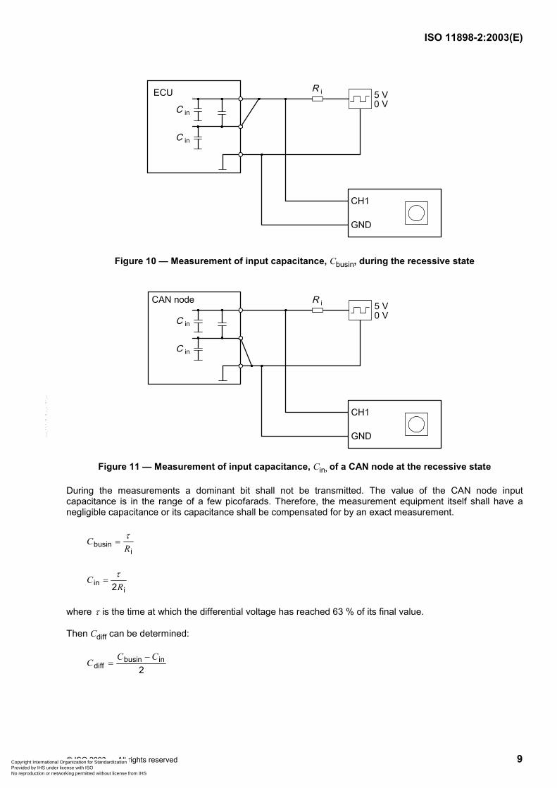
Figure 10 — Measurement of input capacitance, Cbusin, during the recessive state
Figure 11 — Measurement of input capacitance, Cin, of a CAN node at the recessive state
During the measurements a dominant bit shall not be transmitted. The value of the CAN node input capacitance is in the range of a few picofarads. Therefore, the measurement equipment itself shall have a negligible capacitance or its capacitance shall be compensated for by an exact measurement.
busini
CRτ
=
ini2
CRτ
=
where τ is the time at which the differential voltage has reached 63 % of its final value.
Then Cdiff can be determined:
busin indiff 2
C CC
−=
Copyright International Organization for Standardization Provided by IHS under license with ISO
Not for ResaleNo reproduction or networking permitted without license from IHS
The measurement of the internal delay time tnode shall be undertaken by applying a dominant bit at the CAN bus inputs of an error active CAN node in idle state. The CAN node shall regard the dominant bit as a start of frame (SOF) and perform a hard resynchronization. The CAN controller shall detect a stuff error at the sixth recessive bit after the dominant bit and respond with an active error flag. The time measured between the externally applied dominant bit and the beginning of the error flag is tedge_to_edge.
The sync term can be eliminated by adjusting the phasing to get the maximum value for tedge_to_edge (maximization of the CAN cell sampling error: 1 tq).
The measurement of the ECU internal delay time is illustrated in Figure 12.
Values in volts
Figure 12 — Measurement of the ECU internal delay time
Using a test method derived from the above to assess tinputRD the test unit synchronizes itself to the SOF sent by the CAN node. Upon detection of the first recessive bit, the test unit shall partly overwrite the duration of this recessive bit by a dominant level, starting backwards from the expected end of the bit (see hatched area). The overwriting is started earlier and earlier until the node eventually loses arbitration and stops transmitting. Figure 13 illustrates this overwriting.
tinputRD + toutputDR = tsample − NBT − tx
This equation may be used to assess the terms tinputRD and toutputRD for the network synchronization.
Copyright International Organization for Standardization Provided by IHS under license with ISO
Not for ResaleNo reproduction or networking permitted without license from IHS
Figure 13 — Synchronization by overwriting recessive bits by dominant bit of test unit
7 Electrical specification of HS-MAU
7.1 General
The following electrical specification is valid for a two-wire differential bus with transmission rates up to 1 Mbit/s. The termination shown in Figure 1 and Figure 14 is specified in Table 10. It is not recommended to integrate the termination into a CAN node.
a) Termination A b) Termination B
Figure 14 — Bus termination of the high-speed bus implementation
7.2 Physical medium attachment sublayer specification
7.2.1 General
The parameters specified in Tables 1 to 5 shall be adhered to throughout the operating condition range of every CAN node. The parameters are chosen such that a maximum number of CAN nodes may be connected to the common bus.
Copyright International Organization for Standardization Provided by IHS under license with ISO
Not for ResaleNo reproduction or networking permitted without license from IHS
Table 1 — Bus voltage parameters for recessive state
Value Parameter Notation Unit
min. nom. max.Condition
VCAN_H V 2,5 7,0 Common mode bus voltage
VCAN_L V −2,0 2,5
Measured with respect to the individual ground of each CAN node
Differential bus voltage a Vdiff mV −120 0 12 Measured at each CAN node connected to the bus.
a The differential bus voltage is determined by the output behaviour of all CAN nodes during the recessive state. Therefore Vdiff is
approximately zero (see Table 4). The min. value is determined by the requirement that a single bus driver shall be able to represent a dominant bit by a min. value of Vdiff = 1,2 V.
Table 2 — Bus voltage parameters for dominant state
Value Parameter Notation Unit
min. nom. max. Condition
VCAN_H V 3,5 7,0 Common mode bus voltage a
VCAN_L V −2,0 1,5
Measured with respect to the individual ground of each CAN node
Differential bus voltage b Vdiff V 1,2 2,0 3,0 Measured at each CAN node connected to the bus.
a The min. value of VCAN_H is determined by the min. value of VCAN_L plus the min. value of Vdiff. The max. value of VCAN_L is determined by the max. value of VCAN_H minus the min. value of Vdiff . b The bus load increases as CAN nodes are added to the network, by Rdiff. Consequently, Vdiff decreases. The min. value of Vdiffdetermines the number of CAN nodes allowed on the bus. The max. value of Vdiff is specified by the upper limit during arbitration.
Table 3 — Maximum ratings of VCAN_L and VCAN_H of CAN node
Voltage a
V Nominal battery voltage V Notation
min. max.
VCAN_H − 3,0 16,0 12
VCAN_L − 3,0 16,0
VCAN_H − 3,0 32,0 24
VCAN_L − 3,0 32,0 a Undisturbed operation does not have to be guaranteed, but no destruction of bus driver circuit and no time limit.
Copyright International Organization for Standardization Provided by IHS under license with ISO
Not for ResaleNo reproduction or networking permitted without license from IHS
Table 4 — DC parameters for recessive output of CAN node
Value Parameter Notation Unit
min. nom. max. Condition
VCAN_H V 2,0 2,5 3,0 Output bus voltage
VCAN_L V 2,0 2,5 3,0 no load
Differential output bus voltage Vdiff mV − 500 0 50 no load
Differential internal resistance Rdiff kΩ 10 100 no load a
Internal resistor b Rin kΩ 5 50
Differential input voltage c Vdiff V − 1,0 0,5 d, e
a The load is connected between CAN_H and CAN_L. For a CAN node without integrated terminating resistor RL (normal use); this resistor is a RL/2 resistor. For CAN nodes with an integrated terminating resistor, this is a RL resistor. In this case, RL is seen between CAN_H and CAN_L instead of Rdiff (see 6.5.2).
b Rin of CAN_H and CAN_L should have almost the same value (see 6.5.1). The deviation shall be less than 3 % relative to each other.
c The threshold for receiving the dominant and recessive bits ensures a noise immunity of 0,3 V and 0,5 V respectively. The lower value for the dominant state is motivated by the fact that a lower load resistance between CAN_H and CAN_L is seen (the capacitance of the supply voltage source is the reason that the internal resistance of the bus driver driving the dominant bit is connected in parallel to the bus load resistance).
d Threshold for receiving a recessive bit. e Reception shall be ensured within the common mode voltage range specified in Table 1 and Table 2.
Table 5 — DC parameters for dominant output of CAN node
Value Parameter Notation Unit
min. nom. max. Condition
VCAN_H V 2,75 3,5 4,5 Output bus voltage
VCAN_L V 0,5 1,5 2,25 load RL/2 a
Differential output voltage Vdiff V 1,5 2,0 3,0 load RL/2 a
Differential input voltage b Vdiff V 0,9 5,0 load RL/2 a, c, d a The load is connected between CAN_H and CAN_L. For a CAN node without integrated terminating resistor (normal use), this resistor is a RL/2 resistor. For CAN nodes with an integrated terminating resistor, this is a RL resistor. In this case, RL is seen between CAN_H and CAN_L instead of Rdiff. b The threshold for receiving the dominant and recessive bits ensures a noise immunity of 0,3 V and 0,5 V respectively. The lower value for the dominant state is motivated by the fact that a lower load resistance between CAN_H and CAN_L is seen (the capacitance of the supply voltage source is the reason that the internal resistance of the bus driver driving the dominant bit is connected in parallel to the bus load resistance). c Threshold for receiving a dominant bit.
d Reception shall be ensured within the common mode voltage range specified in Table 1 and Table 2.
7.2.2 Bus levels
7.2.2.1 Common mode voltages
The parameters specified in Table 1 apply when all CAN nodes are connected to a correctly terminated bus.
7.2.2.2 Disturbance by coupling
The tolerated disturbances of CAN_H and CAN_L by coupling are defined in accordance with ISO 7637-3:1995, test pulses 3a and 3b.
Copyright International Organization for Standardization Provided by IHS under license with ISO
Not for ResaleNo reproduction or networking permitted without license from IHS
The parameters given in Table 3 shall be tested at the CAN_L and CAN_H pins of each CAN node, with the CAN node disconnected from the bus (see 6.2 and 6.3).
The parameters given in Tables 4 and 5 shall be tested at the CAN_L and CAN_H pins of each CAN node, according to conformance tests 6.2 to 6.7 of ISO 16845.
7.3.2 Illustration of voltage range
Load conditions are specified in Tables 1 to 5. Figures 15 to 18 illustrate the valid voltage ranges of VCAN_H and VCAN_L.
Key
ts Random time. a Nominal. b Range of VCAN_H.
Figure 15 — Valid voltage range of VCAN_H during recessive state of CAN node disconnected from bus if VCAN_L varies from min. to max. voltage level
Copyright International Organization for Standardization Provided by IHS under license with ISO
Not for ResaleNo reproduction or networking permitted without license from IHS
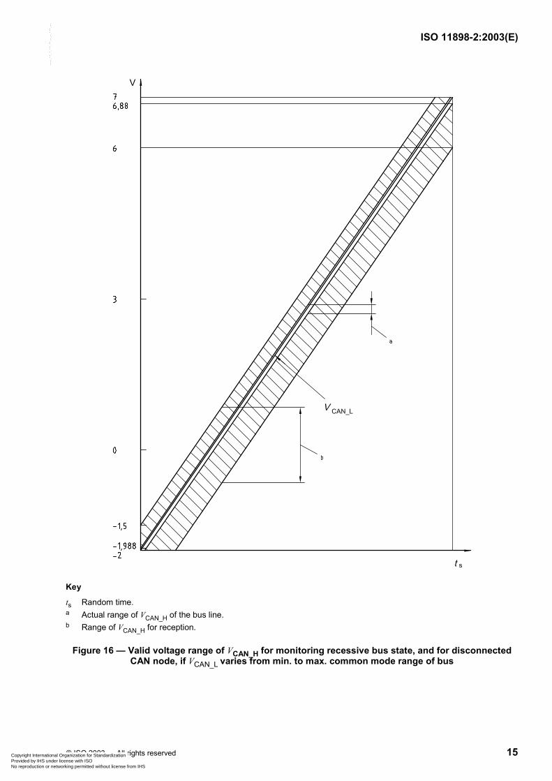
ts Random time. a Actual range of VCAN_H of the bus line. b Range of VCAN_H for reception.
Figure 16 — Valid voltage range of VCAN_H for monitoring recessive bus state, and for disconnected CAN node, if VCAN_L varies from min. to max. common mode range of bus
Copyright International Organization for Standardization Provided by IHS under license with ISO
Not for ResaleNo reproduction or networking permitted without license from IHS
ts Random time. a Actual range of VCAN_H of the bus line. b Range of VCAN_H for reception.
Figure 18 — Valid voltage range of VCAN_H for monitoring dominant bus state, and for disconnected CAN node, if VCAN_L varies from min. to max. common mode range of bus
The parameters given in Table 6 shall be tested at the CAN_L and CAN_H pins of each CAN node, according to the conformance tests specified in Clause 6 of ISO 16845.
Table 6 — AC parameters of CAN node disconnected from bus
Value Parameter Notation Unit
min. nom. max. Condition
Bit time tB µs 1 a
Internal capacitance Cin pF 20 c
Differential internal capacitance b Cdiff pF 10 1 Mbit/s a The min. bit time corresponds to a max. bit rate of 1 Mbit/s. The lower end of the bit rate depends on the protocol IC. b In addition to the internal capacitance restriction, a bus connection should also have as low an inductance as possible. This is particularly important for high bit rates. The min. values of Cin and Cdiff may be zero. The max. tolerable values are determined by the bit timing and the network topology parameters l and d (see the footnote to Table 11). Proper functionality is guaranteed if occurring cable-reflected waves do not suppress the dominant differential voltage levels below Vdiff = 0,9 V and do not increase the recessive differential voltage level above Vdiff = 0,5 V at each individual CAN node (see Table 4 and Table 5). c 1 Mbit/s for CAN_H and CAN_L relative to HF ground.
Copyright International Organization for Standardization Provided by IHS under license with ISO
Not for ResaleNo reproduction or networking permitted without license from IHS
A connector used to plug CAN nodes to the bus shall be in accordance with Table 8.
Table 8 — Connector parameters
Value Parameter Notation Unit
min. nom. max.
VBAT = 12 V U V 16 Voltage
VBAT = 24 V U V 32
Current I mA 0 25 80
Peak current a IP mA 500
Transmission frequency f MHz 25
Transmission resistance b RT mΩ 70 a Time restriction: 101 tB. b The differential voltage of the bus seen by the receiving CAN node depends on the line resistance between this and the transmitting CAN node. Therefore the transmission resistance of the signal wires is limited by the bus level parameters at each CAN node.
7.5 Physical medium specification
7.5.1 General
The specifications given below shall be fulfilled by the cables chosen for the CAN bus. The aim of these specifications is to standardize the electrical characteristics and not to specify mechanical and material parameters of the cable.
Cables for the bus shall be in accordance with the specifications of Table 9.
Copyright International Organization for Standardization Provided by IHS under license with ISO
Not for ResaleNo reproduction or networking permitted without license from IHS
Table 9 — Physical media parameters of a pair of wires (shielded or unshielded)
Value Parameter Notation Unit
min. nom. max.Condition
Impedance Z Ω 95 120 140 Measured between two signal wires
Length-related resistance R mΩ/m 70 a
Specific line delay ns/m 5 b
a The differential voltage on the bus seen by a receiving CAN node depends on the line resistance between it and the transmitting CAN node. Therefore, the total resistance of the signal wires is limited by the bus level parameters of each CAN node. b The min. delay between two points of the bus may be zero. The max. value is determined by the bit time and the delay times of the transmitting and receiving circuitry.
7.5.2 Termination resistor
The termination resistor RL used in termination A and termination B shall comply with the limits specified in Table 10.
Table 10 — Termination resistor
Value Notation Unit
min. nom. max.Condition
RL a
Ω 100 120 130 Min. power dissipation: 220 mW
a Dependent on the topology, the bit rate, and the slew rate, deviations from 120 Ω are possible. It is, however, necessary to check the applicability of other resistor values in each case.
Remark: The lower the termination resistor value, the smaller the number of nodes in the network.
7.5.3 Topology
The wiring topology of a CAN network should be as close as possible to a single line structure in order to avoid cable-reflected waves. Network topology parameters shall be in accordance with Table 11.
Table 11 — Network topology parameters
Value Parameter Notation Unit
min. nom. max.Condition
Bus length L m 0 40
Cable stub length l m 0 0,3
Node distance D m 0,1 40
Bit rate: 1 Mbit/s a
a At bit rates lower than 1 Mbit/s the bus length may be lengthened significantly. Depending on l, the bit rate and internal capacitances of the individual CAN nodes, other network topologies with changed lengths l and d may be used. In this case the influence of occurring cable resonator waves on the bit representation on the bus should be carefully checked by measurements of Vdiff at each CAN node (see also Table 4, Footnote c).
7.6 Bus failure management
During normal operation, several bus failures can occur that influence the bus operation. The resulting behaviour of the network shall be as given in Table 12. The possible open circuit and short circuit failures are shown in Figure 19.
Copyright International Organization for Standardization Provided by IHS under license with ISO
Not for ResaleNo reproduction or networking permitted without license from IHS
Description of bus failure Behaviour of network a Quality of specification b
One node becomes disconnected from the bus The remaining nodes continue communicating. Recommended
One node loses power The remaining nodes continue communicating with reduced signal-to-noise ratio. Recommended
One node loses ground The remaining nodes continue communicating with reduced signal-to-noise ratio. Recommended
Loss of the shield connection at any node c All nodes continue communicating. Recommended
Open and short failures d All nodes continue communicating with reduced signal-to-noise ratio. Recommended
1 CAN_H interrupted
2 CAN_L interrupted
3 CAN_H shorted to battery voltage
4 CAN_L shorted to ground
5 CAN_H shorted to ground
6 CAN_L shorted to battery voltage
7 CAN_L wire shorted to CAN_H wire Optional
8 CAN_H and CAN_L wires interrupted at the same location
Recommended
9 Loss of one connection to termination network
Recommended
a The example in Figure 19 excludes all fault tolerant modes. b The quality of specification is as follows.
If the respective failure occurs the network shall behave as described in the second column of the table.
If the respective failure occurs, the network behaviour should be as described in the second column of the table. Exclusion of this specified functionality is at the manufacturer’s discretion.
If the respective failure occurs the network behaviour may be as described in the second column of the table. Inclusion of this fuller specified functionality is at the manufacturer’s discretion.
c This failure should be considered only if a shielded cable is used. In this case the loss of shield connection at one node may cause common mode voltage induced between the shield and the two signal wires. d The numbers 1 to 9 refer to Cases 1 to 9 in Figure 19.
Copyright International Organization for Standardization Provided by IHS under license with ISO
Not for ResaleNo reproduction or networking permitted without license from IHS