Interplay between emission wavelength and s-psplitting in MOCVD-grown InGaAs/GaAs quantumdots emitting above 1.3 lm
Cite as: Appl. Phys. Lett. 116, 023102 (2020); doi: 10.1063/1.5124812Submitted: 16 August 2019 . Accepted: 5 January 2020 .Published Online: 16 January 2020
Paweł Podemski,1,a) Anna Musiał,1 Krzysztof Gawarecki,2 Aleksander Mary�nski,1 Przemysław Gontar,1
Artem Bercha,3 Witold A. Trzeciakowski,3 Nicole Srocka,4 Tobias Heuser,4 David Quandt,4
Andr�e Strittmatter,4,b) Sven Rodt,4 Stephan Reitzenstein,4 and Grzegorz SeRk1
AFFILIATIONS1Laboratory for Optical Spectroscopy of Nanostructures, Department of Experimental Physics, Wrocław University of Scienceand Technology, 50-370 Wrocław, Poland
2Department of Theoretical Physics, Wrocław University of Science and Technology, 50-370 Wrocław, Poland3Institute of High Pressure Physics, Polish Academy of Sciences, 01-142 Warsaw, Poland4Institute of Solid State Physics, Technische Universit€at Berlin, 10623 Berlin, Germany
a)E-mail: [email protected])Present address: Institute of Experimental Physics, Otto von Guericke University Magdeburg, D-39106 Magdeburg, Germany.
ABSTRACT
The electronic structure of strain-engineered single InGaAs/GaAs quantum dots emitting in the telecommunication O band is probedexperimentally by photoluminescence excitation spectroscopy. The observed resonances can be attributed to p-shell states of individualquantum dots. The determined energy difference between the s-shell and the p-shell shows an inverse dependence on the emission energy.The experimental data are compared with the results of confined state calculations, where the impact of the size and composition in theinvestigated structures is simulated within the 8-band k�p model. On this basis, the experimental observation is attributed mainly to changesin the indium content within individual quantum dots, indicating a way of engineering and selecting a desired quantum dot whose electronicstructure is the most suitable for a given nanophotonic application.
Published under license by AIP Publishing. https://doi.org/10.1063/1.5124812
Security of data transmission has become an important issue ininformation technology. Today, most information is stored andexchanged digitally, with most transfers being secured by public-keycryptography. However, the development of quantum computing hasshown disturbingly easy ways to overcome classical cryptographysecurity, which assumes limited computer performance. In particular,Shor’s algorithm has demonstrated that number factorization (andthus the data decryption) can be performed in computation timeshorter by a polynomial factor.1 This has led to intensive researchfocusing on truly secure communication—quantum cryptography.2
For practical realization of device-independent quantum key distribu-tion and quantum communication via optical fibers, single-photonsources operating at telecommunication wavelengths are key buildingblocks.3
One of the most promising systems for realizing single-photonsources based on non-classical light emitters is semiconductor
quantum dots (QDs),4 which have been shown to work well at tele-communication wavelengths, e.g., in the low dispersion and low loss Oband.5–7 Moreover, for this spectral range, optical-fiber-compatiblesingle-photon sources based on quantum dots have been demon-strated.8–10 Further optimization of the optical properties of such sour-ces is required to increase the collection efficiency and the fabricationyield, for instance, by decreasing the QD areal density and by deter-ministic integration of QDs into optical microcavities or other pho-tonic structures increasing the extraction of the emitted photons.11 Toobtain efficient emission in the telecom O band, InGaAs QDs onthe GaAs substrate (typically emitting below 1lm) can be used inconjunction with an InGaAs strain-reducing layer (SRL), shifting theemission to the desired 1.3lm.12–16 The incorporation of an addi-tional layer in the vicinity of QDs during the growth process influencesthe local strain and therefore their size and composition, as well as thedepth of the confining potential, modifying the electronic structure
Appl. Phys. Lett. 116, 023102 (2020); doi: 10.1063/1.5124812 116, 023102-1
expected for common and well-established InGaAs/GaAs QDs emit-ting below 1lm (i.e., those without additional strain-reducing layers).Therefore, to fully understand and use these as quantum light sources,it is essential to identify their electronic structure. In particular, thehighest purity of single-photon emission of InGaAs QDs can beobtained using the p-shell excitation scheme,17 and this requires pre-cise knowledge of the confined exciton excited state spectrum of indi-vidual QDs, including the p-shell state energies. Moreover, for thedesign of these sources, it would be beneficial to have the possibility toaffect or tailor both the QD ground state energy (i.e., emission wave-length) and the energetic distance from the ground state to the excitedstate, preferably separated by at least thermal energy at a given opera-tion temperature from the emitting quantum dot ground state, to pro-vide high thermal stability and spectral isolation. Therefore, it iscrucial to identify the main determinants of the electronic structure ofthese application-relevant epitaxial nanostructures, which are espe-cially important for the envisioned nanophotonic applications, such asefficient sources of single photons or entangled photon pairs emittingat telecommunication wavelengths compatible with existing fiber net-works. Although some attempts with quasi-resonant excitation havebeen performed for quantum-optical experiments,9 there is no system-atic study on the interrelation between the emission wavelength andenergy separation between the ground and excited states in single, Oband-emitting InGaAs/GaAs QDs with the strain-reducing layer or onidentification of the decisive structural properties.
In this report, we determine the energetic splitting betweens-shell and p-shell states (s-p splitting) in single InGaAs/GaAs QDsemitting in the O band, and we show how the s-p splitting can beinfluenced by the QD composition, the size, and the In content inthe SRL. The investigated sample was grown by metalorganic chemi-cal vapor deposition (MOCVD) on a GaAs substrate with 23 pairs ofGaAs/Al0.9Ga0.1As layers forming a distributed Bragg reflector(DBR), providing increased emission collection efficiency from thelayer of QDs. InGaAs quantum dots (with a nominal indium contentof 0.75) were formed during Stranski–Krastanov self-assembledgrowth followed by capping with 4 nm of In0.2Ga0.8As8, creating astrain-reducing layer, resulting in the indium concentration and QDsizes favoring 1.3lm emission. Finally, a 630-nm-thick GaAs layerwas grown, from which an array of microlenses (with no specific QDpreselection) was produced by means of 3D electron-beam lithogra-phy.18,19 In this etching process, QDs outside lenses were removed,leaving areas of QDs with a base diameter of 3.6lm. The areal den-sity of these QDs was of the order of 109 cm�2 with their base diame-ter of 30 nm and an average height of 6–8nm.9,20 A reference samplewas also used with an ensemble of similar QDs with a slightly differ-ent indium composition and with no DBR below the dot layer to pre-vent overlapping of the DBR characteristics with the spectrally broademission of a QD ensemble in the spectroscopic studies. To identifyexcited states in these quantum dots, single-dot photoluminescenceexcitation (PLE) spectroscopy adapted to the spectral range above1lm was used.21 QDs were excited by a self-made continuous waveexternal-cavity tunable laser followed by a short-focal-length mono-chromator and shortpass filters to provide a clean excitation laserline. For nonresonant excitation, a 639nm semiconductor laser wasused. The QD sample was mounted in a continuous-flow microscopycryostat providing temperatures down to 5K. To excite single QDsand collect their emission, an achromatic objective with a 0.4
numerical aperture was applied, offering a laser spot diameter on thesample surface of single micrometers, which was small enough toexcite selectively single microlenses. QD emission spectra weredetected using a nitrogen-cooled linear array InGaAs sensor coupledto a monochromator.
The standard photoluminescence (PL) spectrum of the unpat-terned reference sample with the whole ensemble of InGaAs QDs ispresented in Fig. 1(a). This shows the spectral range of QD emissionfor nonresonant excitation (639nm; 1.940 eV) with the excitationpower density of 4 kW/cm2. Two maxima related to the radiativerecombination in QDs, which exhibit the typical state filling effectwith increasing excitation power (not shown here), can be observed.Thus, the left maximum corresponds to the QD ground state (s-shell)emission, while the presence of the second maximum is attributed tothe recombination in a higher (p-shell) QD state and not to a multi-modal size distribution.22 The reference sample with an ensemble ofsimilar QDs has been studied in detail in Ref. 20. The energy differencebetween the QD maxima is approximately 70meV, indicating theexpected splitting energy between s-shell and p-shell exciton stateswithin a single InGaAs QD. This value is relatively large as comparedto conventional InGaAs QDs emitting below 1lm17,23 and shouldprovide high thermal stability of the ground state emission. On thehigh energy slope of the second maximum, a fingerprint of an evenhigher quantum dot state, separated by approximately 130meV fromthe ground state, can be observed—confirming a rather deep confiningpotential of the investigated QDs. Figure 1(b) presents an exemplaryphotoluminescence spectrum from a single QD excited quasi-resonantly (1242nm; 0.998 eV; i.e., into the expected p-shell state,based on the high-excitation PL of the QD ensemble) with the excita-tion power density of 1 kW/cm2, with several sharp emission linesobserved in the O band spectral range.
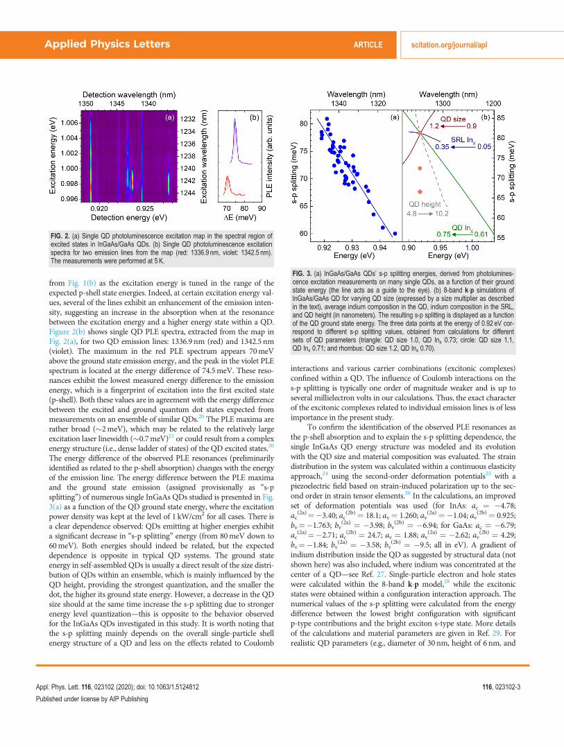
An example of a complete PLE map from single InGaAs QDs ispresented in Fig. 2(a). This shows an evolution of the emission lines
FIG. 1. (a) Photoluminescence spectrum of a reference sample with an ensembleof InGaAs/GaAs QDs obtained under non-resonant excitation conditions (639 nm;1.940 eV) with estimated energy differences between consecutive QD states. (b)Single QD photoluminescence spectrum for quasi-resonant excitation (1242 nm;0.998 eV) of InGaAs/GaAs QDs. Both spectra were recorded at 5 K.
from Fig. 1(b) as the excitation energy is tuned in the range of theexpected p-shell state energies. Indeed, at certain excitation energy val-ues, several of the lines exhibit an enhancement of the emission inten-sity, suggesting an increase in the absorption when at the resonancebetween the excitation energy and a higher energy state within a QD.Figure 2(b) shows single QD PLE spectra, extracted from the map inFig. 2(a), for two QD emission lines: 1336.9 nm (red) and 1342.5 nm(violet). The maximum in the red PLE spectrum appears 70meVabove the ground state emission energy, and the peak in the violet PLEspectrum is located at the energy difference of 74.5meV. These reso-nances exhibit the lowest measured energy difference to the emissionenergy, which is a fingerprint of excitation into the first excited state(p-shell). Both these values are in agreement with the energy differencebetween the excited and ground quantum dot states expected frommeasurements on an ensemble of similar QDs.20 The PLE maxima arerather broad (�2meV), which may be related to the relatively largeexcitation laser linewidth (�0.7meV)21 or could result from a complexenergy structure (i.e., dense ladder of states) of the QD excited states.20
The energy difference of the observed PLE resonances (preliminarilyidentified as related to the p-shell absorption) changes with the energyof the emission line. The energy difference between the PLE maximaand the ground state emission (assigned provisionally as “s-psplitting”) of numerous single InGaAs QDs studied is presented in Fig.3(a) as a function of the QD ground state energy, where the excitationpower density was kept at the level of 1 kW/cm2 for all cases. There isa clear dependence observed: QDs emitting at higher energies exhibita significant decrease in “s-p splitting” energy (from 80meV down to60meV). Both energies should indeed be related, but the expecteddependence is opposite in typical QD systems. The ground stateenergy in self-assembled QDs is usually a direct result of the size distri-bution of QDs within an ensemble, which is mainly influenced by theQD height, providing the strongest quantization, and the smaller thedot, the higher its ground state energy. However, a decrease in the QDsize should at the same time increase the s-p splitting due to strongerenergy level quantization—this is opposite to the behavior observedfor the InGaAs QDs investigated in this study. It is worth noting thatthe s-p splitting mainly depends on the overall single-particle shellenergy structure of a QD and less on the effects related to Coulomb
interactions and various carrier combinations (excitonic complexes)confined within a QD. The influence of Coulomb interactions on thes-p splitting is typically one order of magnitude weaker and is up toseveral millielectron volts in our calculations. Thus, the exact characterof the excitonic complexes related to individual emission lines is of lessimportance in the present study.
To confirm the identification of the observed PLE resonances asthe p-shell absorption and to explain the s-p splitting dependence, thesingle InGaAs QD energy structure was modeled and its evolutionwith the QD size and material composition was evaluated. The straindistribution in the system was calculated within a continuous elasticityapproach,24 using the second-order deformation potentials25 with apiezoelectric field based on strain-induced polarization up to the sec-ond order in strain tensor elements.26 In the calculations, an improvedset of deformation potentials was used (for InAs: ac ¼ �4.78;ac
bv¼�1.84; bv(2a) ¼ �3.58; bv(2b) ¼ �9.5; all in eV). A gradient ofindium distribution inside the QD as suggested by structural data (notshown here) was also included, where indium was concentrated at thecenter of a QD—see Ref. 27. Single-particle electron and hole stateswere calculated within the 8-band k�p model,28 while the excitonicstates were obtained within a configuration interaction approach. Thenumerical values of the s-p splitting were calculated from the energydifference between the lowest bright configuration with significantp-type contributions and the bright exciton s-type state. More detailsof the calculations and material parameters are given in Ref. 29. Forrealistic QD parameters (e.g., diameter of 30 nm, height of 6 nm, and
FIG. 2. (a) Single QD photoluminescence excitation map in the spectral region ofexcited states in InGaAs/GaAs QDs. (b) Single QD photoluminescence excitationspectra for two emission lines from the map (red: 1336.9 nm, violet: 1342.5 nm).The measurements were performed at 5 K.
FIG. 3. (a) InGaAs/GaAs QDs’ s-p splitting energies, derived from photolumines-cence excitation measurements on many single QDs, as a function of their groundstate energy (the line acts as a guide to the eye). (b) 8-band k�p simulations ofInGaAs/GaAs QD for varying QD size (expressed by a size multiplier as describedin the text), average indium composition in the QD, indium composition in the SRL,and QD height (in nanometers). The resulting s-p splitting is displayed as a functionof the QD ground state energy. The three data points at the energy of 0.92 eV cor-respond to different s-p splitting values, obtained from calculations for differentsets of QD parameters (triangle: QD size 1.0, QD Inx 0.73; circle: QD size 1.1,QD Inx 0.71; and rhombus: QD size 1.2, QD Inx 0.70).
lens shape of QD) the calculated QD ground state energy is 0.92 eVwith the s-p splitting energy of approximately 80meV, correspondingwell to the measured PLE resonances, thus confirming the identifica-tion of the observed experimental maxima. Next, the influence of theQD size on the s-p splitting energy was simulated and the result isshown in Fig. 3(b)—the QD size is changed relatively to the above-mentioned dimensions (see the red curve) with the size multiplierindicated in the figure—all QD dimensions are changed simulta-neously, which is typically expected, in the first approximation, forsuch III-V self-assembled QDs.13,30,31 A decrease in the QD size shiftsthe ground state energy to higher values and increases the s-p splitting,which is in contrast to the experimentally observed dependence. Theother parameter expected to alter the electronic structure in InGaAsQDs is the indium content. Its influence on the s-p splitting energywas calculated for the strain-reducing layer and QDs, independently,and is also presented in Fig. 3(b). Here, the In content corresponds tothe average In amount within the QD and to the In content in SRL,where no composition gradient is assumed. These results show similartrends as observed in the experiment—higher ground state energy isassociated with lower s-p splitting values. Thus, the dominant factorresponsible for s-shell and p-shell separation in InGaAs QDs coveredby an SRL is not their size but the indium content. Changing the SRLcontent exclusively gives a significantly weaker dependence than theexperimental one and would be able to cover only a small part of theexperimentally obtained values and only for unrealistically broad Incontent range fluctuations from 5% to 35%. Therefore, this factormust be of secondary importance. In contrast, modifying the QD com-position gives the s-p splitting vs emission energy dependence muchcloser to the experimental data, for still realistic In contents.
The average indium content in the simulated QD was changedfrom 0.75 down to 0.61. For the quantum dot emitting at 0.92 eV, theaverage In content in the dot (obtained within the simulated gradientdistribution) is 0.73, which is slightly lower than the nominal indiumcontent of 0.75, but still very close (e.g., the accuracy of the experimen-tally determined In content in Ref. 27 was 60.13). In the simulations,the maximum In content in the gradient was 1.0, which correspondsto the average In content of 0.75. This value constitutes the upper limitof the possible In content for the assumed In distribution within theQD. To reproduce the experimental data, QDs with an average indiumcontent down to 0.61 were also simulated, which suggests a lower Incontent in the investigated QDs emitting at higher energies. It is worthnoting that an increase in the average indium content (i.e., InAsamount within the InGaAs alloy) leads to lower ground state energy,but at the same time, the effective mass is reduced, resulting in thelarger separation between s-shell and p-shell states. The change in theindium content also influences the lattice mismatch between InGaAsand GaAs, and the resulting strain field has an impact on the QDenergy structure—this effect was taken into account in the calcula-tions. For the investigated QDs, all the simulated parameters (i.e., QDsize; QD composition; SRL composition) do change within the ensem-ble simultaneously. Therefore, the absolute energy values from thesimulations do not correspond to the experimental s-p slitting valuesprecisely but support (or do not) the observed trends.
In general, one can expect that s-p splitting energy is also influ-enced by the QD aspect ratio. For comparison, the effect of varyingthe QD height is also shown in Fig. 3(b) as a gray dashed line wherethe indium composition gradient is also rescaled accordingly in the
QD height direction, while the base QD size remains constant. It isworth noting that the ground state energy is increasing for higherQDs, which shows that its changes are driven predominantly by thestrain and not by the spatial confinement. Although the obtained s-psplitting dependence could, in principle, reflect the experimentalobservation, we consider this scenario as unlikely to occur. First, asmentioned above, during the growth of self-assembled QDs, the aspectratio does not usually change significantly, i.e., the increase in the QDdiameter is followed by a simultaneous increase in the dotheight.13,30,31 Second, in order to cover the experimental range ofemission energies, one would need to assume a very broad change inthe QD height (with a constant QD base diameter), up to exceeding10nm, which is already at the limit for plastic relaxation32 and deterio-rates QD radiative properties. Some changes in the QDs’ height cannotbe ruled out from our considerations, and these perhaps contribute tothe obtained inverse s-p splitting vs emission energy dependence.However, taking into account all the limitations, the latter seems to bedriven by the QD composition predominantly. It is worth commentingthat in previous studies, a higher indium content in InGaAs/GaAs QDswas linked to the smaller nanostructure size; however, those QDs weregrown by molecular beam epitaxy and were emitting below 1lm, andso this tendency does not have to transfer directly to other QDs in thesame material system.33
In our structures, the s-p splitting can be influenced by the QDsize and composition change in opposite ways, as related to the QDground state energy—see the red and green lines in Fig. 3(b). Thisdemonstrates the possibility of mutual tuning of QD ground andexcited state energies, offering an additional degree of freedom inquantum nanodevice engineering. In Fig. 3(b), three points are shownfor simulated QDs emitting at 0.92 eV, but with different s-p splittingvalues ranging from 81 to 67meV. This result was obtained for differ-ent pairs of QD sizes and indium average content within the QDvolume—triangle: size 1.0, Inx 0.73; circle: size 1.1, Inx 0.71; rhombus:size 1.2, Inx 0.70. In general, it is possible to obtain different s-p split-ting values for QDs emitting at the same wavelength, when both theparameters (QD size and composition) are controlled. However, suchstraightforward control is beyond what is achievable technologicallyduring the growth of QD structures, as it is impossible to keep the QDsize constant and change the composition only. Nevertheless, the QDground state and s-p splitting can be controlled at the whole ensemblelevel by a mutual change in the QD size and indium composition, forinstance, by overgrowth of the quantum dot layer with InGaAs orthermally induced diffusion. From such an ensemble, individual QDsproviding ground state and s-p splitting energy values, required for agiven application, can be selected.
When looking at the calculated s-p splitting for electron and holesingle particle states, it is shared approximately 35:65 between the valenceand conduction bands, respectively, corresponding to 19–26meV forholes and 35–48meV for electrons (depending on the specific QD), withapproximately 6meV provided in addition by the Coulomb interaction.This offers an energetic separation large enough to prevent any signifi-cant thermally induced losses, resulting in the overall thermal stability ofdevices based on such InGaAs QDs, especially in current solutions thatstill require cryogenic temperatures to operate, where the obtained sepa-ration of 80meV between s-shell and p-shell states is sufficiently high,e.g., to allow for stand-alone operation in a compact Stirling cryocoolerwith base temperatures in the range of 30–40K.34
In general, tailoring the s-p splitting could also have an impacton other parameters important for a quantum source efficiency, e.g.,signal-to-background ratio, single-photon emission, or fine-structuresplitting. This has been partly considered in Refs. 9 and 27 but requiresa further study to obtain accurate statistical information (e.g., onsingle-photon emission), and so this is beyond the scope of this report.
In summary, we have studied InGaAs/GaAs QDs capped with astrain-reducing layer, providing the QD emission redshift to the tele-com O band. Single QD photoluminescence excitation spectroscopyhas allowed us to determine the energy splitting between the s-shelland the p-shell in individual QDs, revealing a reduced splitting fordots emitting at higher energies. Supported by theoretical modeling,this behavior has been considered to be dominated by a varyingindium content in different QDs within the ensemble. A secondaryeffect that could result in the observed dependence is the QD aspectratio. However, its distribution within a QD ensemble is expected tobe narrow, and therefore, the influence on the s-p splitting energy israther small. The ability to influence the interplay between the groundstate emission and the s-p splitting energy indicates an additionaldegree of freedom in the design and growth of QDs for O band spec-tral range applications, such as telecom single-photon sources withp-shell quasi-resonant optical pumping.9 In particular, this allows usto obtain an improved spectral isolation of the ground state transition,e.g., to increase the activation energy for carriers’ escape via higherenergy states in a QD and provide high temperature stability. Theinvestigated structures were grown by MOCVD, which is also of prac-tical importance, since this technology offers lower production costsand, hence, is better suited for large-scale device fabrication thanmolecular beam epitaxy.
We acknowledge financial support from the National ScienceCentre (Poland) within Project No. 2014/15/D/ST3/00813; the FI-sequr project jointly financed by the European RegionalDevelopment Fund (EFRE) of the European Union in theframework of the programme to promote research, innovation, andtechnologies (Pro FIT) in Germany and the National Centre forResearch and Development in Poland within the 2nd Poland-BerlinPhotonics Programme, Grant No. 2/POLBER-2/2016 (Project valuePLN 2,089,498); the Polish National Agency for AcademicExchange; and the “Quantum dot-based indistinguishable andentangled photon sources at telecom wavelengths” project, carriedout within the HOMING programme of the Foundation for PolishScience co-financed by the European Union under the EuropeanRegional Development Fund.
REFERENCES1P. Shor, SIAM J. Comput. 26, 1484 (1997).2H.-K. Lo, M. Curty, and K. Tamaki, Nat. Photonics 8, 595 (2014).3N. Sangouard and H. Zbinden, J. Mod. Opt. 59, 1458 (2012).4Nano-Optics and Nanophotonics: Quantum Dots for Quantum InformationTechnologies, ed. P. Michler (Springer, 2017).
5F. Klopf, R. Krebs, J. P. Reithmaier, and A. Forchel, IEEE Photonics Technol.Lett. 13, 764 (2001).
6M. Sartison, L. Engel, S. Kolatschek, F. Olbrich, C. Nawrath, S. Hepp, M. Jetter,P. Michler, and S. L. Portalupi, Appl. Phys. Lett. 113, 032103 (2018).
7A. Rantam€aki, G. S. Sokolovskii, S. A. Blokhin, V. V. Dudelev, K. K. Soboleva,M. A. Bobrov, A. G. Kuzmenkov, A. P. Vasil’ev, A. G. Gladyshev, N. A.Maleev, V. M. Ustinov, and O. Okhotnikov, Opt. Lett. 40, 3400 (2015).
8M. B. Ward, O. Z. Karimov, D. C. Unitt, Z. L. Yuan, P. See, D. G. Gevaux, A. J.Shields, P. Atkinson, and D. A. Ritchie, Appl. Phys. Lett. 86, 201111 (2005).
9Ł. Dusanowski, P. Holewa, A. Mary�nski, A. Musiał, T. Heuser, N. Srocka, D.Quandt, A. Strittmatter, S. Rodt, J. Misiewicz, S. Reitzenstein, and G. SeRk, Opt.Express 25, 31122 (2017).
10J. Kettler, M. Paul, F. Olbrich, K. Zeuner, M. Jetter, and P. Michler, Appl. Phys.B 122, 48 (2016).
11P. Schneider, N. Srocka, S. Rodt, L. Zschiedrich, S. Reitzenstein, and S. Burger,Opt. Express 26, 8479 (2018).
12E. Goldmann, M. Paul, F. F. Krause, K. M€uller, J. Kettler, T. Mehrtens, A.Rosenauer, M. Jetter, P. Michler, and F. Jahnke, Appl. Phys. Lett. 105, 152102(2014).
13F. Guffarth, R. Heitz, A. Schliwa, O. Stier, N. N. Ledentsov, A. R. Kovsh, V. M.Ustinov, and D. Bimberg, Phys. Rev. B 64, 085305 (2001).
14B. Alloing, C. Zinoni, V. Zwiller, L. H. Li, C. Monat, M. Gobet, G. Buchs, A.Fiore, E. Pelucchi, and E. Kapon, Appl. Phys. Lett. 86, 101908 (2005).
15A. E. Zhukov, A. R. Kovsh, N. A. Maleev, S. S. Mikhrin, V. M. Ustinov, A. F.Tsatsul’nikov, M. V. Maximov, B. V. Volovik, D. A. Bedarev, Y. M.Shernyakov, P. S. Kop’ev, Z. I. Alferov, N. N. Ledentsov, and D. Bimberg, Appl.Phys. Lett. 75, 1926 (1999).
16L. Seravalli, M. Minelli, P. Frigeri, P. Allegri, V. Avanzini, and S. Franchi, Appl.Phys. Lett. 82, 2341 (2003).
17P. Ester, L. Lackmann, S. Michaelis de Vasconcellos, M. C. H€ubner, A. Zrenner,and M. Bichler, Appl. Phys. Lett. 91, 111110 (2007).
18M. Gschrey, A. Thoma, P. Schnauber, M. Seifried, R. Schmidt, B. Wohlfeil, L.Kr€uger, J.-H. Schulze, T. Heindel, S. Burger, F. Schmidt, A. Strittmatter, S.Rodt, and S. Reitzenstein, Nat. Commun. 6, 7662 (2015).
19N. Srocka, A. Musiał, P.-I. Schneider, P. Mrowi�nski, P. Holewa, S. Burger, D.Quandt, A. Strittmatter, S. Rodt, S. Reitzenstein, and G. SeRk, AIP Adv. 8,085205 (2018).
20A. Mary�nski, P. Mrowi�nski, K. Ryczko, P. Podemski, K. Gawarecki, A. Musiał,J. Misiewicz, D. Quandt, A. Strittmatter, S. Rodt, S. Reitzenstein, and G. SeRk,Acta Phys. Pol. A 132, 386 (2017).
21P. Podemski, A. Mary�nski, P. Wyborski, A. Bercha, W. Trzeciakowski, and G.SeRk, J. Lumin. 212, 300 (2019).
22U. W. Pohl, K. P€otschke, A. Schliwa, F. Guffarth, D. Bimberg, N. D. Zakharov,P. Werner, M. B. Lifshits, V. A. Shchukin, and D. E. Jesson, Phys. Rev. B 72,245332 (2005).
23A. Zrenner, F. Findeis, E. Beham, M. Markmann, G. B€ohm, and G. Abstreiter,Physica E 9, 114 (2001).
24C. Pryor, J. Kim, L. W. Wang, A. J. Williamson, and A. Zunger, J. Appl. Phys.83, 2548 (1998).
25K. Gawarecki and M. Zieli�nski, Phys. Rev. B 100, 155409 (2019).26G. Bester, A. Zunger, X. Wu, and D. Vanderbilt, Phys. Rev. B 74, 081305(2006).
27P. Mrowi�nski, A. Musiał, K. Gawarecki, Ł. Dusanowski, T. Heuser, N. Srocka,D. Quandt, A. Strittmatter, S. Rodt, S. Reitzenstein, and G. SeRk, Phys. Rev. B100, 115310 (2019).
28T. B. Bahder, Phys. Rev. B 41, 11992 (1990).29K. Gawarecki, Phys. Rev. B 97, 235408 (2018).30D. Litvinov, H. Blank, R. Schneider, D. Gerthsen, T. Vallaitis, J. Leuthold, T.Passow, A. Grau, H. Kalt, C. Klingshirn, and M. Hetterich, J. Appl. Phys. 103,083532 (2008).
31A. Sauerwald, T. K€ummell, G. Bacher, A. Somers, R. Schwertberger, J. P.Reithmaier, and A. Forchel, Appl. Phys. Lett. 86, 253112 (2005).
32J. F. Chen, Y. C. Lin, C. H. Chiang, R. C. C. Chen, Y. F. Chen, Y. H. Wu, and L.Chang, J. Appl. Phys. 111, 013709 (2012).
33A. Musiał, P. Gold, J. Andrzejewski, A. L€offler, J. Misiewicz, S. H€ofling, A.Forchel, M. Kamp, G. SeRk, and S. Reitzenstein, Phys. Rev. B 90, 045430 (2014).
34A. Schlehahn, S. Fischbach, R. Schmidt, A. Kaganskiy, A. Strittmatter, S. Rodt,T. Heindel, and S. Reitzenstein, Sci. Rep. 8, 1340 (2018).