Abstract: A specific class of planar photonic crystals is investigatedthat provides a condensed matter combining the properties of planarmultilayer stacks and two-dimensional photonic crystals in order toachieve large partial bandgaps in the eigenstate spectrum.These gapsare larger than the directionally dependent and polarization-dependentpartial gaps of photonic crystal slabs. Full in-plane gaps are demonstratednumerically. Strong dispersion, waveguide confinement, high Q-cavities,and alternative photonic signal processing are feasible with these structures.
OCIS codes:(050.0050) Diffraction and gratings; (130.0000) Integrated optics; (230.0000)Optical devices
References and links1. E. Yablonovitch, “Inhibited spontaneous emission in solid-state physics and electronics,” Phys. Rev. Lett.58,
2059-2062 (1987).2. S. John, “Strong localization of photons in certain disordered dielectric superlattices,” Phys. Rev. Lett.58, 2486-
2489 (1987).3. J. D. Joannopoulos, R .D. Meade, and J. N. Winn,Photonic Crystals(Princeton U. Press, Princeton, N. J., 1995).4. S. Y. Lin, E. Chow, V. Hietala, P. R. Villeneuve, and J. D. Joannopoulos, “Experimental demonstration of guiding
and bending of electromagnetic waves in a photonic crystal,”Science282, 274-276 (1998).5. S. Y. Lin, E. Chow, S. G. Johnson, and J. D. Joannopoulos, “Demonstration of highly efficient waveguiding in a
photonic crystal slab at the 1.5−µmwavelength,” Opt. Lett.25, 1297-1299 (2000).6. E. Chow, S. Y. Lin, J. R. Wendt, S. G. Johnson, and J. D. Joannopoulos, “Quantitative analysis of bending
efficiency in photonic-crystal waveguide bends atλ = 1.55µmwavelengths,” Opt. Lett.26, 286-288 (2001).7. S. Y. Lin, E. Chow, S. G. Johnson, and J. D. Joannopoulos, “Direct measurement of the quality factor in a
two-dimensional photonic-crystal microcavity,” Opt. Lett.26, 1903-1905 (2001).8. T. Søndergaard and K. H. Dridi, ”Energy flow in photonic crystal waveguides,” Phys. Rev. B.61, 15688-15696
(2000).9. K. M. Ho, C. T. Chan, and C. M. Soukoulis, “Existence of a photonic gap in periodic dielectric structures,” Phys.
Rev. Lett.65, 3152-3155 (1990).10. E. Yablonovitch, T. J. Gmitter, and K. M. Leung, “Photonicband structure: the face-centered-cubic case employ-
ing nonspherical atoms,” Phys. Rev. Lett.67, 2295-2298 (1991).11. S. G. Johnson and J. D. Joannopoulos, “Three-dimensionally periodic dielectric layered structure with omnidi-
rectional photonic band gap,” Appl. Phys. Lett.77, 3490-3492 (2000).12. S. Fan, P. R. Villeneuve, R. D. Meade, and J. D. Joannopoulos, “Design of three-dimensional photonic crystals
at submicron lengthscales,” Appl. Phys. Lett.65, 1466-1468 (1994).13. S. Noda, K. Tomoda, N. Yamamoto, and A. Chutinan, “Full three-dimensional photonic bandgap crystals at
near-infrared wavelengths,” Science289, 604-606 (2000).14. O. Toader and S. John, “Proposed square spiral microfabrication architecture for large three-dimensional pho-
tonic band gap crystals,” Science292, 1133-1135 (2001).15. E. Kuramochi, M. Notomi, T. Tamamura, T. Kawashima, S. Kawakami, J. Takahashi, and C. Takahashi, “Drilled
alternating-layer structure for three-dimensional photonic crystals with a full band gap,” J. Vac. Sci. Technol. B18, 3510-3513 (2000).
(C) 2003 OSA 19 May 2003 / Vol. 11, No. 10 / OPTICS EXPRESS 1156#2261 - $15.00 US Received March 24, 2003; Revised May 07, 2003
16. S. Kawakami, E. Kuramochi, M. Notomi, T. Kawashima, J. Takahashi, C. Takahashi, and T. Tamamura, “A newfabrication technique for photonic crystals: nanolithography combined with alternating-layer deposition,” Opt.Quantum Electron.34, 53-61 (2002).
17. S. G. Johnson, S. Fan, P. R. Villeneuve, J. D. Joannopoulos, and L. A. Kolodziejski, “Guided modes in photoniccrystal slabs,” Phys. Rev. B.60, 5751-5758 (1999).
18. S. G. Johnson, P. R. Villeneuve, S. Fan, and J. D. Joannopoulos, “Linear waveguides in photonic-crystal slabs,”Phys. Rev. B.62, 8212-8222 (2000).
19. Y. Fink, J.N. Winn, S. Fan, C. Chen, J. Michel, J. D. Joannopoulos, and E. L. Thomas, “A dielectric omnidirec-tional reflector,” Science282, 1679-1682 (1998).
20. J. N. Winn, Y. Fink, S. Fan, and J. D. Joannopoulos, “Omnidirectional reflection from a one-dimensional photoniccrystal,” Opt. Lett.23, 1573-1575 (1998).
21. M. Deopura, C. K. Ullal, B. Temelkuran, and Y. Fink, “Dielectric omnidirectional visible reflector,” Opt. Lett.26, 1197-1199 (2001).
22. B. Temelkuran, E. L. Thomas, J. D. Joannopoulos, and Y. Fink, “Low-loss infrared dielectric material system forbroadband dual-range omnidirectional reflectivity,” Opt. Lett.26, 1370-1372 (2001).
23. M. Ibanescu, Y. Fink, S. Fan, E. L. Thomas, and J. D. Joannopoulos, “An all-dielectric coaxial waveguide,”Science289, 415-419 (2000).
24. S. G. Johnson, M. Ibanescu, M. Skorobogatiy, O. Weisberg, T. Engeness, M. Soljacic, S. A. Jacobs, J. D.Joannopoulos, and Y. Fink, “Low-loss asymptotycally single-mode propagation in large-core OmniGuide fibers,”Opt. Express9, 748 (2001),http://www.opticsexpress.org/abstract.cfm?URI=OPEX-9-13-748
25. C. Hooijer, D. Lenstra, and A. Lagendijk, “Mode density inside an omnidirectional mirror is heavily directionalbut not small,” Opt. Lett.25, 1666-1668 (2000).
26. S. G. Johnson and J. D. Joannopoulos, “Block-iterative frequency-domain methods for Maxwell’s equations in aplanewave basis,” Opt. Express8, 173 (2001),http://www.opticsexpress.org/abstract.cfm?URI=OPEX-8-3-173
27. Z. Y. Li and Y. Xia, “Omnidirectional absolute band gaps intwo-dimensional photonic crystals,” Phys. Rev. B.64, 153108-153112 (2001).
28. B. Temelkuran, S. D. Hart, G. Benoit, J. D. Joannopoulos, and Y. Fink, “Wavelength-scalable hollow opticalfibres with large photonic bandgaps forCO2 laser transmission,” Nature420, 650-653 (2002).
1. Introduction
Photonic crystals (PCs) made of dielectric materials are structures with a spatially periodic vari-ation of dielectric constant. In 1987 it was suggested that photons in subwavelength periodicdielectric structures might be controlled in pretty much the same way that electrons are in a pe-riodic electrical potential of atoms and molecules in a crystal lattice of semiconductor material[1, 2]. In the past ten years scientific research has clarifiedsome of the remarkable propertiesof one-, two-, and three-dimensional PCs through extensivetheoretical and numerical studies[3] and through experimental validation [4, 5, 6, 7]. Photonic bandgaps in the spectrum of al-lowed photonic energy states in condensed matter arise frommultiple destructive interferenceof electromagnetic waves resulting from multiple scattering and diffraction effects in periodicdielectric structures with geometric features in the subwavelength regime of operation. Theenergy flow in such structures shows that photons can experience a photonic potential barrierin multidimensional periodic gratings or PCs by diffraction [8] just as electrons experience anelectrical potential barrier in a crystal lattice of atoms.
Two-dimensional (2D) PCs allow the characterization of modes into TE (electric field vectorparallel to the 2D plane) and TM (magnetic field vector parallel to the 2D plane) polariza-tion states and can exhibit complete, polarization-dependent 2D bandgaps, or partial bandgapsin the spatial frequency-frequency domain{(k,ω)} in which we study the spectrum of spa-tiotemporal signals of the space-time domain{(r , t)}. However, these crystals cannot confineelectromagnetic radiation in the third dimension, becauseof their 2D nature. A series of three-dimensional (3D) PCs that exhibit complete 3D bandgaps for all polarized states have beenproposed and studied theoretically in the past 12 years [9, 10, 11, 12, 13, 14, 15, 16]. All thesestructures have a true 3D nature with complex unit cells and are made of materials with highdielectric contrast with a high filling fraction of low indexmaterial. They require very precisethree-dimensional alignment and numerous intermediate steps in the material processing whose
(C) 2003 OSA 19 May 2003 / Vol. 11, No. 10 / OPTICS EXPRESS 1157#2261 - $15.00 US Received March 24, 2003; Revised May 07, 2003
physical chemistry implies several processing temperatures, gaseous byproducts, material andgeometric grain impurities inducing mechanical stress that can disturb the optical quality ofthe final product. These facts make the microfabrication of these structures rather difficult andthe use of electron beam lithography instead of photolithography does not make them easilyamenable for mass production. Furthermore, the creation oflocalized cavities and line defectsin these structures is not an obvious task. Instead, some effort has lately been directed at us-ing quasi-3D structures where the planar confinement of light is achieved through a 2D PCwhile the vertical confinement results from total internal reflection [17, 18, 5, 6]. However,the bandgaps in PC slabs that have a symmetry plane parallel to the slab surface are guidedmode gaps and have been found to be polarization dependent and only cover a reduced area in(k,ω) space, i.e., they are partial gaps under the light cone, meaning that radiation in the topand lower cladding is allowed even for frequencies in the partial bandgap. This is problematicbecause guided modes localized in line defects in such structures are operating in a pseudogapthat covers an even smaller area of(k,ω) space [18] and it has been shown experimentally thatlight in such defects is not strongly confined [6] as the efficiency of waveguide bends is onlyacceptable for a very narrow frequency range within the frequency band of the pseudogap.
Recently, a very important observation was made by noticingthat a complete three-dimensional bandgap is not a necessary requirement for obtaining high-omnidirectional re-flectivity [19, 20, 21, 22]. External high omnidirectional reflectivity has been demonstratedfor waves travelling in air and incident upon the one-dimensional multilayer stack of alternat-ing layers with high index contrasts. The symmetries of thisstructure have been exploited inthe design of a cylindrical coaxial omnidirectional waveguide with very promising properties[23, 24], but the manufacture of such a fiber remains a challenge as good accuracy is neededin order to maintain the periodicity in the rotationally symmetric structure. The bandgaps inthis fiber are only possible because the angular wave-vectorcomponent,kφ , goes to zero as theobservation point moves away from the fiber-axis (p. 752 in [24]). Without this fact there wouldbe no bandgap. One-dimensional planar multilayer stacks exhibiting external omnidirectionalreflection relative to a surrounding filled with air are efficient reflectors, but their eigenstates donot result in band diagrams with large in-plane bandgaps as shown in [25]. Hooijeret al.haveshown that omnidirectional reflection is not a sufficient signature of a photonic bandgap [25].Although dramatic angular redistribution takes place, themode density of the electromagneticfield is hardly altered within the planar omnidirectional reflection range. The latter is due tothe huge dielectric contrast, and the mode characteristicsresemble that of a waveguide. Thisis seen in band diagrams. Therefore, air or low index channeldefects positioned within a bulkplanar 1D omnidirectional stack cannot localize energy viabandgaps. A planar technology thatwould allow similar electromagnetic localization as that of the cylindrical omniguide fibers ina massive background of high omnidirectional reflection andavoid the complexity of truely3D PCs might enable advanced all-optical signal processingin reduced volumes of condensedmatter. For many photonic applications, energy transport aside, the cylindrical form is not nec-essarily an advantage. In this article we present a highly generic class of planar PCs that exhibitlarge partial bandgaps in the eigenstate spectrum. These gaps are larger than the direction-ally dependent and polarization-dependent partial gaps ofphotonic crystal slabs. These widergaps are obtained at the expense of a little extra processingcomplexity. Full in-plane gaps aredemonstrated numerically. It is not claimed nor demonstrated that total external and internalreflectivity can be achieved in defects created inside the presented structures, but the large in-trinsic bandgaps suggest that strong dispersion, waveguide confinement, high Q-cavities, andalternative photonic signal processing can be expected.
(C) 2003 OSA 19 May 2003 / Vol. 11, No. 10 / OPTICS EXPRESS 1158#2261 - $15.00 US Received March 24, 2003; Revised May 07, 2003
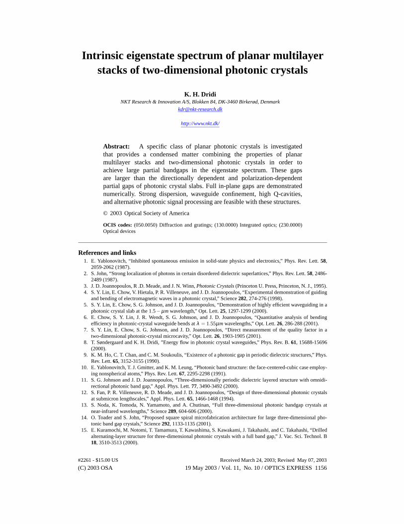
Fig. 1. Multilayer stacks of 2D photonic crystals that exhibit large bandgaps in their modespectrum (from left to right MS2DPC1 and MS2DPC2). MS2DPC1 is madeof a 1D di-electric multilayer stack of alternating planar layersA andB filled with materialsA andB,respectively, in which a 2D crystal lattice of cylindrical holes is etched andwhere the holesmight be filled with materialC. MS2DPC2 is made of a 2D crystal lattice of cylindrical pil-lars grown in a background materialC. These pillars are made of a 1D dielectric multilayerstack of alternating planar layers with materialsA andB.
2. Planar multilayer stacks of photonic crystal slabs
Figure 1 shows two types of multilayer stacks of 2D photonic crystals that exhibit largebandgaps in their mode spectrum (from left to right MS2DPC1 and MS2DPC2). MS2DPC1is made of a 1D dielectric multilayer stack of alternating planar layers of materialsA andB,respectively, in which a 2D crystal lattice of cylindrical holes is etched, where these might befilled with materialC. MS2DPC2 is made of a 2D crystal lattice of cylindrical pillars grown in abackground materialC. These pillars are made of a 1D dielectric multilayer stack of alternatingplanar layers with materialsA andB.
With reference to the Cartesian coordinate system of Fig. 1,a MS2DPC operates in a waythat the 1D structure creates a local bandgap for electromagnetic modes of radiation propagat-ing along thez−axis, while the 2D structure creates a local bandgap for electromagnetic modesof radiation propagating along directions parallel to the(x,y) plane, i.e., parallel to the layersurfaces in the stack. When these two bandgaps overlap in{(k,ω)} space, the eigenstates arestrongly redistributed in a way that large bandgaps are possible for many directions of propaga-tion. This redistribution does not automatically mean thatthe total density of states is low, butat least modes are locally suppressed. The 1D periodicity along thez−axis is characterized byΛz = tAz+ tBz, wheretAz andtBz are the respective layer thicknesses. The 2D crystal lattice ischaracterized by the nature of the lattice (quadratic, triangular, honeycomb, etc ...), the latticeconstantΛ, and the material distribution in the spatial unit cell. In the structures of Fig. 1 wedefiner0 to be the radius of the filled cylinders, and denote bynA, nB, andnC the respectiverefractive indices, and byNzΛz the total height of these structures. The following theoreticaland numerical investigations relate to structures whereNz is infinite in order to understand thegeneral electrodynamics. In realityNz is finite and something between four and twenty unitswill suffice depending on the application and the spatiotemporal radiation rate in a specificconfiguration. The theoretical investigations in this article rely on numerical results from thesolution of a magnetic field formulation of Maxwell’s equations for determining electromag-netic eigenstates of general polarization in structures with spatial inversion symmetry wherethe fields are expanded in a plane wave basis, and where an iterative method for minimizing
(C) 2003 OSA 19 May 2003 / Vol. 11, No. 10 / OPTICS EXPRESS 1159#2261 - $15.00 US Received March 24, 2003; Revised May 07, 2003
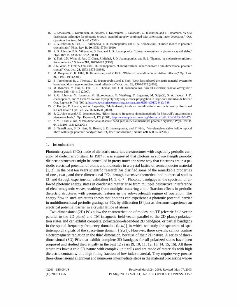
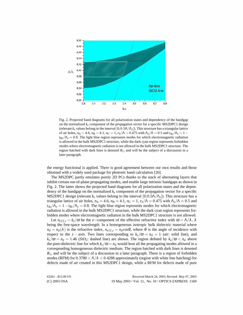
Fig. 2. Projected band diagrams for all polarization states and dependency of the bandgapon the normalizedkz component of the propagation vector for a specific MS2DPC1 design(relevantkz values belong to the interval[0;0.5Λ/Λz]). This structure has a triangular latticeof air holes,nA = 4.6, nB = 4.1, nC = 1, r0/Λ = 0.475 withΛz/Λ = 0.5 andtAz/Λz = 1−tBz/Λz = 0.8. The light blue region represents modes for which electromagnetic radiationis allowed in the bulk MS2DPC1 structure, while the dark cyan region represents forbiddenmodes where electromagnetic radiation is not allowed in the bulk MS2DPC1 structure. Theregion hatched with dark lines is denotedR1, and will be the subject of a discussion in alater paragraph.
the energy functional is applied. There is good agreement between our own results and thoseobtained with a widely used package for photonic band calculation [26].
The MS2DPC partly emulates purely 2D PCs thanks to the stack of alternating layers thatinhibit certain out-of-plane propagating modes, and enable large intrinsic bandgaps as shown inFig. 2. The latter shows the projected band diagrams for all polarization states and the depen-dency of the bandgap on the normalizedkz component of the propagation vector for a specificMS2DPC1 design (relevantkz values belong to the interval[0;0.5Λ/Λz]). This structure has atriangular lattice of air holes,nA = 4.6, nB = 4.1, nC = 1, r0/Λ = 0.475 withΛz/Λ = 0.5 andtAz/Λz = 1− tBz/Λz = 0.8. The light blue region represents modes for which electromagneticradiation is allowed in the bulk MS2DPC1 structure, while the dark cyan region represents for-bidden modes where electromagnetic radiation in the bulk MS2DPC1 structure is not allowed.
Let ne f f,z = kz/ω be thez−component of the effective refractive index withω = Λ/λ , λbeing the free-space wavelength. In a homogeneous isotropic bulk dielectric material wherend = nd(λ ) is the refractive index,ne f f,z = ndcosθ , whereθ is the angle of incidence withrespect to thez− axis. Two lines corresponding tokz/ω = nd = 1 (air: solid line), andkz/ω = nd = 1.46 (SiO2: dashed line) are shown. The region defined bykz/ω < nd abovethe pure-dielectric line for whichkz/ω = nd would host all the propagating modes allowed in acorresponding homogeneous dielectric medium. The region hatched with dark lines is denotedR1, and will be the subject of a discussion in a later paragraph.There is a region of forbiddenmodes (RFM) for 0.3780< Λ/λ < 0.4288 approximately (region with white line hatching) fordefects made of air created in this MS2DPC1 design, while a RFM for defects made of pure
(C) 2003 OSA 19 May 2003 / Vol. 11, No. 10 / OPTICS EXPRESS 1160#2261 - $15.00 US Received March 24, 2003; Revised May 07, 2003
silica is non-existent. However, complete three-dimensional omnidirectional reflection is not anecessary requirement for photonic-bandgap-guiding in channel defects created in a MS2DPC.That is because the(k,ω) mode with localized energy guided by the photonic bandgap need notcouple energy into radiation states with higherkz values. This is observed in photonic crystalslabs for in-plane propagating modes [17, 18, 5, 6] althoughthe radiation in line defect bends inthe latter is substantial because the in-plane gap forkz = 0, which is polarization dependent, isonly partial and coupling to radiation modes at line defect bends is allowed. This radiation lossmight be minimized in a MS2DPC background because of a full in-plane bandgap forkz = 0,which is not the case for photonic crystal slabs. Whether the full in-plane bandgap forkz = 0enables strong in-plane localization and guiding or not in the xy-plane in channels filled withdielectric materials with low or high refractive index shall be investigated in future work. Itshould be possible to exploit the large RFM for strong localization and dispersion as well aseffective redistribution of electromagnetic signals in waveguides created inside or adjacent to aMS2DPC.
The rotationally symmetric omniguides of [23, 24] are basedon the 1D omnidirectional re-flector of [19]. In these structures the bandgap of the bulk material is large and only dependson the 1D multilayer stack design, but rotational symmetry is needed in order to guide electro-magnetic modes and avoid significant leakage of energy. In the MS2DPC the bandgap mostlydepends on the 2D PC in layersA and B, and are therefore a little narrower, but rotationalsymmetry in a cylindrical fiber is no longer a requirement forenergy-guiding defects with lowleakage, at least for strongly localized bound modes. The proposed planar structures offer otherphotonic storage/manipulation and signal processing opportunities because miniaturized highQ cavities and(k,ω) dispersion managing components can be processed locally ona chipthrough deposition and etching techniques. This is advantageous for e.g. Wavelength DivisionMultiplexing (WDM) in telecommunications and sensor technologies.
In this article we primarily focus on MS2DPC1 with a triangular lattice of holes filled withair. Letωl (kz) andωu(kz) denote the lower and upper normalized frequencies on the edges of thebandgap, andωe(kz) represent the eventual end of the bandgap region whereωl (kz) = ωu(kz).The two bandgap edgesωl (kz) andωu(kz) are ascending functions ofkz because largerkz valuesimply modes that experience more propagation in the regionswith lower index of refraction (themodes experience a lower effective index). The curves ofωl (kz) andωu(kz) are not paralleland the narrowing and eventual closing of the bandgap regionat ωe(kz) happens because twofields of two different frequencies propagating in a direction out-of plane experience differenteffective periodicities along that direction (two such fields incident from an air interface wouldexperience different bending and diffraction angles). Oneof the more attractive features of aMS2DPC is that creating internal defects filled with a dielectric material might enable energyto be efficiently trapped/localized for a long time in resonators, cavities, or waveguides wherestrong dispersion enables alternative signal processing.
3. Polarization characteristics of electromagnetic eigenstates
In the 1D omnidirectional reflector the region of omnidirectional reflection is limited by theTM-like polarization [19]. By filtering away certain polarization states, or by efficiently cou-pling into specific polarization states in structures that inhibit the propagation of certain polar-ized states in well determined directions or planes, we may take advantage of a larger effectivebandgap. In order to analyse the effective polarization of eigenstates we estimate the averagemagnetic/electric energy stored in the Cartesian components of the magnetic/electric field inthe unit cell of the crystal such that
EFd =〈d ·Fd|d ·Fd〉
〈F|F〉,
(C) 2003 OSA 19 May 2003 / Vol. 11, No. 10 / OPTICS EXPRESS 1161#2261 - $15.00 US Received March 24, 2003; Revised May 07, 2003
0
0.1
0.2
0.3
0.4
0.5
0.6
Γ M K Γ
Λ/λ
P1P2
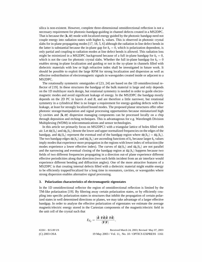
Fig. 3. Band diagram forkz = 0 for all polarization states of the specific MS2DPC of Fig. 2near the gap. The eigenstates are clearly polarized in this window of the spectrum, and arecategorized into theP1 and theP2 polarization types.
whered is one of the Cartesian coordinatesx, y, or z, andF is the magnetic or the electric field.Figure 3 shows the band diagram forkz = 0 for all polarization states of the specific MS2DPCof Fig. 2 near the gap. The eigenstates are clearly polarizedin this window of the spectrum,and are categorized into theP1 and theP2 polarization types. In Fig. 3 theP1 bands are evenmodes, while theP2 bands are odd modes. Numerically we define theP1 states as those havingEEz < 0.1, and theP2 states as those havingEEz > 0.1. TheP1 polarization roughly has the non-zero components(Hz,Ex,Ey) for kz = 0 (TE-like or HE), and theP2 polarization roughly hasthe non-zero components(Ez,Hx,Hy) (TM-like or EH) for kz = 0 (in-plane propagation). If wedefine the incident plane as being the plane which is span by thek andz vectors, the classical spolarization (Ez = 0 andH parallel to the incident plane) is a subgroup of theP1 eigenstates. Instructures involving photonic crystal slabs however the classification into s and p polarizationsis not that practical because of the many dielectric interfaces and surface normals [17, 18]. Thetotal polarization-independent bandgap forkz = 0 is determined by the TM-likeP2 polarization,whereasP1 states experience a larger bandgap covering 0.2870< Λ/λ < 0.4996 approximatelybecause most of the stored electric energy oscillates in theplane where the dielectric contrastis largest and where the photonic potential barrier is greatest due to many more air-dielectricinterfaces which provide strong subwavelength scatteringand destructive interference.
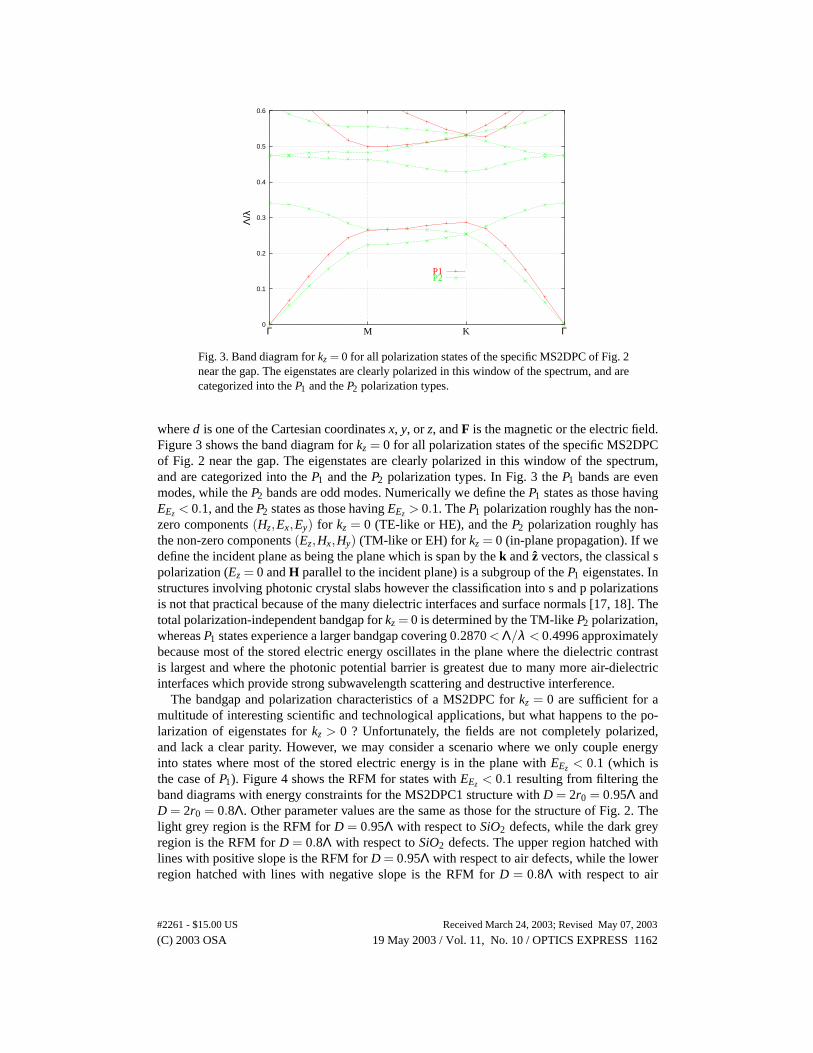
The bandgap and polarization characteristics of a MS2DPC for kz = 0 are sufficient for amultitude of interesting scientific and technological applications, but what happens to the po-larization of eigenstates forkz > 0 ? Unfortunately, the fields are not completely polarized,and lack a clear parity. However, we may consider a scenario where we only couple energyinto states where most of the stored electric energy is in theplane withEEz < 0.1 (which isthe case ofP1). Figure 4 shows the RFM for states withEEz < 0.1 resulting from filtering theband diagrams with energy constraints for the MS2DPC1 structure withD = 2r0 = 0.95Λ andD = 2r0 = 0.8Λ. Other parameter values are the same as those for the structure of Fig. 2. Thelight grey region is the RFM forD = 0.95Λ with respect toSiO2 defects, while the dark greyregion is the RFM forD = 0.8Λ with respect toSiO2 defects. The upper region hatched withlines with positive slope is the RFM forD = 0.95Λ with respect to air defects, while the lowerregion hatched with lines with negative slope is the RFM forD = 0.8Λ with respect to air
(C) 2003 OSA 19 May 2003 / Vol. 11, No. 10 / OPTICS EXPRESS 1162#2261 - $15.00 US Received March 24, 2003; Revised May 07, 2003
Fig. 4. Regions of forbidden modes for states withEEz < 0.1 resulting from filtering theband diagrams with energy constraints for the MS2DPC1 structure withD = 2r0 = 0.95ΛandD = 2r0 = 0.8Λ. Other parameter values are the same as those for the structure of Fig.2. The light grey region is the RFM forD = 0.95Λ with respect toSiO2 defects, while thedark grey region is the RFM forD = 0.8Λ with respect toSiO2 defects. The upper regionhatched with lines with positive slope is the RFM forD = 0.95Λ with respect to air defects,while the lower region hatched with lines with negative slope is the RFM forD = 0.8Λwith respect to air defects.
defects. If we create waveguide defects in a MS2DPC supporting modes withEEz < 0.1 andonly couple energy into such states we can take advantage of alarge region of polarization-dependent energy gap for a wide range of materials in the defect region. Line defects that allowlocalized guided modes withEEz < 0.1 and whose propagation strongly relies on localizationby the photonic potential barrier render the MS2DPC even more interesting. Figure 4 showsthat if we solely operate with the right polarization the region of forbidden radiation relative tomany dielectric materials is enlarged. Furthermore, ther0/Λ parameter enables the movementof the bandgap region and flexible tailoring of photonic bands in the design procedure. Thelower r0/Λ value implies a higher effective refractive index which is why the energy bandsmove toward lowerω values. Air defects yield a region of forbidden modes forP1 states in0.3147< ω < 0.4996 forD = 0.95Λ and in 0.1990< ω < 0.3437 forD = 0.8Λ, while SiO2
defects yield a region of forbidden modes forP1 states in 0.3502< ω < 0.4996 forD = 0.95Λand in 0.2105< ω < 0.3437 forD = 0.8Λ.
It is therefore important to distinguish between polarization-dependent bandgaps andpolarization-independent bandgaps, and between partial bandgaps and extended bandgaps forkz = 0 andkz > 0. In these terms a complete bandgap is a polarization-independent extendedbandgap independent of material andk. Recalling results from purely 2D PCs, the TE polar-ization experiences bandgaps in structures with high indexbackgrounds with relatively highfilling fractions of low index material (thin connecting veins of high index), while the TM po-larization experiences bandgaps in structures with low index backgrounds with relatively lowfilling fractions of high index material (isolated spots of high index). Complete bandgaps in 2DPCs can be found in structures based on the triangular lattice and the honeycomb lattice [3].
(C) 2003 OSA 19 May 2003 / Vol. 11, No. 10 / OPTICS EXPRESS 1163#2261 - $15.00 US Received March 24, 2003; Revised May 07, 2003
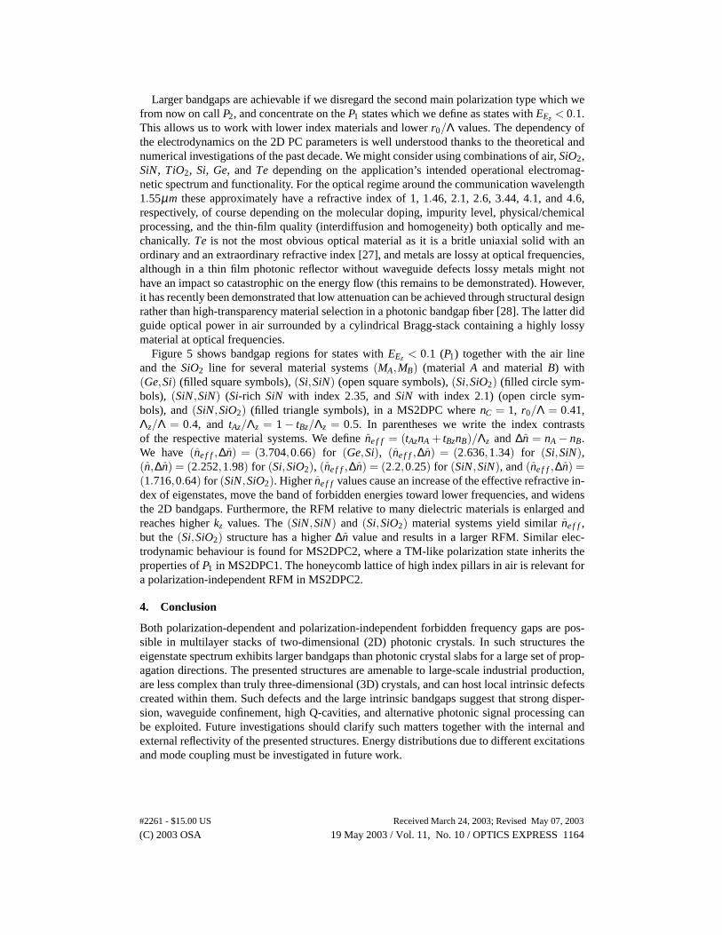
Larger bandgaps are achievable if we disregard the second main polarization type which wefrom now on callP2, and concentrate on theP1 states which we define as states withEEz < 0.1.This allows us to work with lower index materials and lowerr0/Λ values. The dependency ofthe electrodynamics on the 2D PC parameters is well understood thanks to the theoretical andnumerical investigations of the past decade. We might consider using combinations of air,SiO2,SiN, TiO2, Si, Ge, andTe depending on the application’s intended operational electromag-netic spectrum and functionality. For the optical regime around the communication wavelength1.55µm these approximately have a refractive index of 1, 1.46, 2.1, 2.6, 3.44, 4.1, and 4.6,respectively, of course depending on the molecular doping,impurity level, physical/chemicalprocessing, and the thin-film quality (interdiffusion and homogeneity) both optically and me-chanically.Te is not the most obvious optical material as it is a britle uniaxial solid with anordinary and an extraordinary refractive index [27], and metals are lossy at optical frequencies,although in a thin film photonic reflector without waveguide defects lossy metals might nothave an impact so catastrophic on the energy flow (this remains to be demonstrated). However,it has recently been demonstrated that low attenuation can be achieved through structural designrather than high-transparency material selection in a photonic bandgap fiber [28]. The latter didguide optical power in air surrounded by a cylindrical Bragg-stack containing a highly lossymaterial at optical frequencies.
Figure 5 shows bandgap regions for states withEEz < 0.1 (P1) together with the air lineand theSiO2 line for several material systems(MA,MB) (materialA and materialB) with(Ge,Si) (filled square symbols),(Si,SiN) (open square symbols),(Si,SiO2) (filled circle sym-bols), (SiN,SiN) (Si-rich SiN with index 2.35, andSiN with index 2.1) (open circle sym-bols), and(SiN,SiO2) (filled triangle symbols), in a MS2DPC wherenC = 1, r0/Λ = 0.41,Λz/Λ = 0.4, and tAz/Λz = 1− tBz/Λz = 0.5. In parentheses we write the index contrastsof the respective material systems. We definene f f = (tAznA + tBznB)/Λz and ∆n = nA − nB.We have (ne f f,∆n) = (3.704,0.66) for (Ge,Si), (ne f f,∆n) = (2.636,1.34) for (Si,SiN),(n,∆n) = (2.252,1.98) for (Si,SiO2), (ne f f,∆n) = (2.2,0.25) for (SiN,SiN), and(ne f f,∆n) =(1.716,0.64) for (SiN,SiO2). Higherne f f values cause an increase of the effective refractive in-dex of eigenstates, move the band of forbidden energies toward lower frequencies, and widensthe 2D bandgaps. Furthermore, the RFM relative to many dielectric materials is enlarged andreaches higherkz values. The(SiN,SiN) and (Si,SiO2) material systems yield similarne f f,but the(Si,SiO2) structure has a higher∆n value and results in a larger RFM. Similar elec-trodynamic behaviour is found for MS2DPC2, where a TM-like polarization state inherits theproperties ofP1 in MS2DPC1. The honeycomb lattice of high index pillars in air is relevant fora polarization-independent RFM in MS2DPC2.
4. Conclusion
Both polarization-dependent and polarization-independent forbidden frequency gaps are pos-sible in multilayer stacks of two-dimensional (2D) photonic crystals. In such structures theeigenstate spectrum exhibits larger bandgaps than photonic crystal slabs for a large set of prop-agation directions. The presented structures are amenableto large-scale industrial production,are less complex than truly three-dimensional (3D) crystals, and can host local intrinsic defectscreated within them. Such defects and the large intrinsic bandgaps suggest that strong disper-sion, waveguide confinement, high Q-cavities, and alternative photonic signal processing canbe exploited. Future investigations should clarify such matters together with the internal andexternal reflectivity of the presented structures. Energy distributions due to different excitationsand mode coupling must be investigated in future work.
(C) 2003 OSA 19 May 2003 / Vol. 11, No. 10 / OPTICS EXPRESS 1164#2261 - $15.00 US Received March 24, 2003; Revised May 07, 2003
Fig. 5. Bandgap regions for states withEEz < 0.1 (P1) together with the air line and theSiO2line for several material systems(A,B) with (Ge,Si) (filled square symbols),(Si,SiN) (opensquare symbols),(Si,SiO2) (filled circle symbols),(SiN,SiN) (Si-rich SiNwith index 2.35,andSiNwith index 2.1) (open circle symbols), and(SiN,SiO2) (filled triangle symbols), ina MS2DDPC wherenC = 1, r0/Λ = 0.41,Λz/Λ = 0.4, andtAz/Λz = 1− tBz/Λz = 0.5. Inparentheses we write the index contrasts of the respective material systems.
Acknowledgments
I thank NKT Research & Innovation for supporting the photonics program, and particularly K.E. Mattsson, B. H. Larsen, and L. P. Nielsen for valuable discussions in connection with thepresent work.
(C) 2003 OSA 19 May 2003 / Vol. 11, No. 10 / OPTICS EXPRESS 1165#2261 - $15.00 US Received March 24, 2003; Revised May 07, 2003