Chapter 1 Motherboard Description / 1 Introduction System Overview This manual was written to help you start using this product as quickly and smoothly as possbile. Inside, you will find the answers to solve most problems. In order for this reference material to be of greatest use, refer to the expanded table of contents to find relevant topics. This board provides a total PC solution by incorporating the System , I/O , and PCI IDE. The mainboard is designed for Intel PIII/Celeron/Coppermine processors base PC ATX system, support single processors with ISA Bus, AMR Bus, PCI Local Bus, and AGP Bus to support upgrades to your system performance. It is ideal for multi-tasking and fully supports MS-DOS, Windows, Windows NT , Windows ME, Windows 2000 , Novell, OS/2, Windows95/98 , UNIX , Windows98SE, SCO UNIX etc. This manual also explains how to install the mainboard for operation, and how to setup your CMOS configuration with the BIOS setup program.
Transcript
Chapter 1 Motherboard Description / 1
IntroductionSystem OverviewThis manual was written to help you start using this productas quickly and smoothly as possbile. Inside, you will findthe answers to solve most problems. In order for thisreference material to be of greatest use, refer to the�expanded table of contents� to find relevant topics.This board provides a total PC solution by incorporating theSystem , I/O , and PCI IDE. The mainboard is designed forIntel PIII/Celeron/Coppermine processors base PC ATXsystem, support single processors with ISA Bus, AMR Bus,PCI Local Bus, and AGP Bus to support upgrades to yoursystem performance. It is ideal for multi-tasking and fullysupports MS-DOS, Windows, Windows NT , Windows ME,Windows 2000 , Novell, OS/2, Windows95/98 , UNIX ,Windows98SE, SCO UNIX etc.This manual also explains how to install the mainboard foroperation, and how to setup your CMOS configuration withthe BIOS setup program.
2 / Chapter 1 Motherboard Description
1.Motherboard Description1.1 Features1.1.1 HardwareCPU-Socket 370 for Intel PPGA/FC-PGA PII/PIII processor.-Intel FC-PGA/PPGA Celeron Processors300MHz~600MHz or higher processor with 66MHz FSB.-Intel FC-PGA Pentium III Processors 500MHz~933MHzor higher processor with 100/133MHz FSB.-VIA Cyrix III Processors.
Chipset-North Bridge System Chipset : VT82C694X-Sourth Bridge System Chipset: VT82C686A
Biggest memory capacity694XT is equipped with three DIMM socket to support(16MB, 32MB, 64MB, 128MB, 256MB) 168 pin 3.3vSDRAM SPD(Special Presence Detect).Maximummemory up to 768MB.
AGP for fast VGA solution-AGP specification compliant.-AGP 66 MHz 3.3v/1.5v for 2X/4X device support.Note:If an unstable issue occurs, after installing " VIA 4 in 1 driver". We suggest you to re-install " VIA 4 in 1 driver ", and thenselect " install VIA AGP VxD in Standard mode " at" VIA_GART AGP Driver " item.
PCI Expansion SlotProvide one 16 bit ISA, and three 32 bit PCI slots .
On-Board IDE-An IDE controller on the VIA VT82C686A Chipset pro-vides IDE HDD/CD-ROM with PIO,Bus Master and UltraDMA 33/66 operation modes.-Can connect up to four IDE devices.
Chapter 1 Motherboard Description / 3
On-Board Peripherals:-1 floppy port supports 2 FDD with 360K,720K,1.2M,1.44M and 2.88M byte.-2 serial ports (COM1+COM2).-1 parallel port supports SPP/EPP/ECP mode.-1 IrDA/HP connector for SIR.
Audio-AC�97 CODEC on board, support 3D sound.
BIOS- The mainboard BIOS provides �Plug & Play� BIOS which
detects the peripheral devices and expansion cards of theboard automatically.
- The mainboard provides a Desktop Management Interface(DMI) function which records your mainboardspecifications.
- BIOS support CD-ROM, SCSI, LAN BOOT, Temperaturesensor, Wake on modem, LAN, Alarm Bus CLK setup withBIOS.
WOL (Wake On LAN)Supports system power up from LAN ring up .
IrDA PortSupport this serial fast communication up to 115.2Kbps.
Support Ring on by modem/Alarm on (ATX only)Support System power up from Modem ring up or timerof System. Required enabled in Ring on by modem andAlarm on in BIOS.
Supports ACPI function for ATX Power.
Support AT/ATX Power supply(20pin) connector.
4 / Chapter 1 Motherboard Description
1.1.2 SoftwareBIOS-AWARD legal BIOS.-Supports APM 1.2.-Supports USB Function.-Supports ACPIOperation System-Offers the highest performance for MS-DOS, Windows,Windows NT, Windows ME, Windows 2000, Novell, OS/2,Windows95/98, Windows98SE, UNIX, SCO UNIX etc.
1.1.3 Attachments-HDD UDMA66 Cable.-FDD Cable.-Flash Memory Written for BIOS Update.-USB Cable. (option)-Audio Cable.-PS2/Print Port Cable.-COM1/COM2 Cable.-Fully Setup CD Driver built in Utility(Ghost, Anitivirus,Adobe Acrobat...).-This manual.
Chapter 1 Motherboard Description / 5
1.2 Motherboard Installation1.2.1 Layout of Motherboard
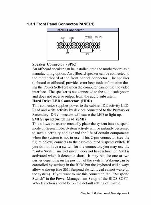
1.3.1 Front Panel Connector(PANEL1)PANEL1 Connector
Speaker Connector (SPK)An offboard speaker can be installed onto the motherboard as amanufacturing option. An offboard speaker can be connected tothe motherboard at the front pannel connector. The speaker(onboard or offboard) provides error beep code information dur-ing the Power Self-Test when the computer cannot use the videointerface. The speaker is not connected to the audio subsystemand does not receive output from the audio subsystem.Hard Drive LED Connector (HDD)This connector supplies power to the cabinet IDE activity LED.Read and write activity by devices connected to the Primary orSecondary IDE connectors will cause the LED to light up.SMI Suspend Switch Lead (SMI)This allows the user to manually place the system into a suspendmode of Green mode. System activity will be instantly decreasedto save electricity and expand the life of certain componentswhen the system is not in use. This 2-pin connector (see thefigure below) connects to the case-mounted suspend switch. Ifyou do not have a switch for the connector, you may use the"Turbo Switch� instead since it does not have a function. SMI isactivated when it detects a short. It may require one or twopushes depending on the position of the switch. Wake-up can becontrolled by settings in the BIOS but the keyboard will alwaysallow wake-up (the SMI Suspend Switch Lead cannot wake-upthe system). If you want to use this connector, the "SuspendSwitch" in the Power Management Setup of the BIOS SOFT-WARE section should be on the default setting of Enable.
SPK
PW_BN
1
2
RST HDD PW_LED
+
+ +
+
SMI
8 / Chapter 1 Motherboard Description
ATX Power Switch (PW_BN)The system power is controlled by a momentary switchconnected to this lead. Pushing the button once will switchthe system ON. The system power LED lights when thesystem's power is on .
Power LED Lead (PW_LED)The system power LED lights when the system power is on.
Reset Switch Lead (RST)The connector can be connected to a momentary SPST typeswitch that is normally open. When the switch is closed,themotherboard resets and runs the POST.
1.3.2 Floppy Disk Connector(FDD1) This connector supports the provided floppy drive ribboncable. After connecting the single end to the board, connectthe two plugs on the other end to the floppy drives.
1.3.3 Hard Disk Connectors(IDE1/IDE2)These connectors support the provided IDE hard disk ribboncable. After connecting the single end to the board, connectthe two plugs at the other end to your hard disk.If you install two hard disks, you must configure the seconddrive to Slave mode by setting its jumper settings. BIOS nowsupports SCSI device or IDE CD-ROM boot up (see "HDDSequence SCSI/IDE First" & "Boot Sequence" in the BIOSFeatures Setup of the BIOS SOFTWARE) (Pin 20 is removedto prevent inserting in the wrong orientation when usingribbon cables with pin 20 plugged) .
Chapter 1 Motherboard Description / 9
1.3.4 ATX/AT Power Supply Connector (20-pin block)- PW1/PW2This connector supports the power button on-board. Usingthe ATX power supply, functions such as Modem Ring Wake-Up and Soft Power Off are supported on this motherboard .This power connector supports instant power-onfunctionality, which means that the system will boot upinstantly when the power connector is inserted on the board.
1.3.5 Infrared Connector(IR)After the IrDA interface is configured, files can betransferred from or to portable devices such as laptops,PDAs, and printers using application software.
This connector will compatible with standard at AT size (largeDIN) keyboard plugs. You may use a DIN to mini DIN adapteron standard AT keyboards.
Mouse PortThis system will direct IRQ12 to PS/2 mouse.
1.4.2 USB Connectors:USB1/USB2The motherboard provides a OHCI(Open Host ControllerInterface)Universal Serial Bus Roots for attaching USBdevices such as a keyboard, mouse and other USB devices.You can plug the USB devices directly into this connector.Four USB ports are available on the back panel.Therefore,we have a solution to provide a 10 pin ribbon cable withbracket to connect Built-in on-board USB header by optional.
13579
VCCP0-P0+GNDGND
246810
GNDGNDP1+P1-VCC
Chapter 1 Motherboard Description / 11
1.5 Serial and Parallel Interface PortsThis system comes equipped with two serial ports and oneparallel port. Both types of interface ports will be explainedin this chapter.
The Serial Interfaces:COM1/COM2The serial interface port is sometimes refered to as an RS-232 port or an asynchronous communication port. Mice,printers, modems and other peripheral devices can beconnected to a serial port. The serial port can also be usedto connect your computer system. If you wish to transferthe contents of your hard disk to another system it can beaccomplished by using each machine�s serial port.
1
COM1/COM2
IR
K/B
PW1
ISA SLOT
MS1
1
JBAT
1
1
FAN1
FAN2
PCI1
PCI2
PCI3
JC1
JC3
JC4
JC5
11
11
COM2
1 1
COM1
1 1
USB
11
1
LPT
AM
R
AGP SLOT
USB
21
1
1
ISA
SOLT
DIM
MPW2
Socket 370
SOCK
ET
AGP
SOLT IDE
FDD
AMR
SOLT
1
AUDIO1 1
WOL
1
JCK4
JCK3
JCK2
JCK1
12 / Chapter 1 Motherboard Description
Parallel Interface PortUnlike serial ports, parallel interface ports have beenstandardized and should not present any difficulty interfacingperipherals to your system. Sometimes called a Centronics port,the parallel port is almost exclusively used with printers.
LPT
IR
K/B
PW1
ISA SLOT
MS1
1
JBAT
1
1
FAN1
FAN2
PCI1
PCI2
PCI3
JC1
JC3
JC4
JC5
11
11
COM2
1 1
COM1
1 1
USB
11
1
LPT
AM
R
AGP SLOT
USB
21
1
1
ISA
SOLT
DIM
M
PW2
Socket 370
SOCK
ET
AGP
SOLT IDE
FDD
AMR
SOLT
1
AUDIO1 1
JCK4
JCK3
JCK2
JCK1
WOL
1
Chapter 1 Motherboard Description / 13
1.6 CPU Installation1.6.1 CPU Installation Procedure:Socket 3701. Pull the lever sideways away from the socket then raisethe lever to a 90-degree angle.2. Locate Pin 1 in the socket and look for the white dot orcut edge in the CPU. Match Pin 1 with the white dot/cutedge then insert the CPU.3. Press the lever down to complete the installation.4.Make sure the spec of the heatsink is good enough.
Notch
IR
K/B
PW1
ISA SLOT
MS1
1
JBAT
1
1
FAN1
FAN2
PCI1
PCI2
PCI3
JC1
JC3
JC4
JC5
11
11
COM2
1 1
COM1
1 1
USB
11
1
LPT
AM
R
AGP SLOT
USB
21
1
1
ISA
SOLT
DIM
MPW2
Socket 370
SOCK
ET
AGP
SOLT IDE
FDD
AMR
SOLT
1
AUDIO1 1
JCK4
JCK3
JCK2
JCK1
WOL
1
14 / Chapter 1 Motherboard Description
1.6.2 CPU Clock Selection: JCK1~JCK4, JC1, JC3The JCK1~4 jumpers are used to set the PCI and CPU external busclock.
F E Q . JCK1 J C K 2 J C K 3 J C K 4 J C 1 J C 3
66MHz 1-2 1-2 2-3 2-3 O P E N O P E N100MHz 1-2 1-2 1-2 2-3 O P E N O P E N133MHz 1-2 1-2 1-2 1-2 O P E N O P E NAuto 1-2 1-2 O P E N O P E N 2-3 CLOSE(Intel)Auto 1-2 1-2 O P E N O P E N 1-2 CLOSE(VIA-Cyrix)
Close : (SHORT)
O p e n :
IR
K/B
PW1
ISA SLOT
MS1
1
JBAT
1
1
FAN1
FAN2
PCI1
PCI2
PCI3
JC1
JC3
JC4
JC5
11
11
COM2
1 1
COM1
1 1
USB
11
1
LPT
AM
R
AGP SLOT
USB
21
1
1
ISA
SOLT
DIM
M
PW2
Socket 370
SOCK
ET
AGP
SOLT IDE
FDD
AMR
SOLT
1
AUDIO1 1
WOL
1
JCK4
JCK3
JCK2
JCK1
Chapter 1 Motherboard Description / 15
1.7 Jumper SettingA jumper has two or more pins that can be covered by a plastic jumper cap, allowing you to select different systemoptions.
1.7.1 CPU/System Fan Connector:Fan1/2
Pin Assignment1 Ground2 +12VDC3 Signal
FAN 2Connector
1
3
2
J1
WOL1Connector
JBAT1
FAN 1Connector
JC2JC1JC3JC4JC5
IR
K/B
PW1
ISA SLOT
MS1
1
JBAT
1
1
FAN1
FAN2
PCI1
PCI2
PCI3
JC1
JC3
JC4
JC5
11
11
COM2
1 1
COM1
1 1
USB
11
1
LPT
AM
R
AGP SLOT
USB
21
1
1
ISA
SOLT
DIM
M
PW2
Socket 370
SOCK
ET
AGP
SOLT IDE
FDD
AMR
SOLT
1
AUDIO1 1
JCK4
JCK3
JCK2
JCK1
WOL
1
16 / Chapter 1 Motherboard Description
1.7.3 AMR Set Function: J1Pin Assignment
Enabled AMR Slot(Default)
Disabled AMR Slot
1.7.4 CMOS Function Selection: JBAT1Pin Assignment1-2 Normal (Default)
2-3 Clear CMOS
NOTE:(Please follow the procedure below to clear CMOS data.)(1)Remove the AC power line.(2)JBAT1(2-3)Closed.(3)Wait fiveseconds.(4)JBAT1(1-2) Closed.(5)AC Power on.(6)Reset yourdesired password or clear CMOS data.
1.7.2 Wake-On LAN Header: WOL1Pin Assignment1 5VSB2 Ground3 Signal3
1
Chapter 1 Motherboard Description / 17
1.7.5 CPU Type Select: JC1~JC2, JC4~JC5Current PCI bus in limited to 33MHz, socket370 Celeronprocessors limited to 66MHz, and SDRAM limited to theDIMM type 66/100/133MHz. Other settings are forexperienced users only.
IR
K/B
PW1
ISA SLOT
MS1
1
JBAT
1
1
FAN1
FAN2
PCI1
PCI2
PCI3
JC1
JC3
JC4
JC5
11
11
COM2
1 1
COM1
1 1
USB
11
1
LPT
AM
R
AGP SLOT
USB
21
1
1
ISA
SOLT
DIM
M
PW2
Socket 370
SOCK
ET
AGP
SOLT IDE
FDD
AMR
SOLT
1
AUDIO1 1
WOL
1
JCK4
JCK3
JCK2
JCK1
CPU Type JC1 JC2 JC4 JC5Intel old(PPGA)
Intel new(FC-PGA)
VIA-Cyrix
JC4JC2 JC5JC1
JC4JC2 JC5JC1
JC4JC2 JC5JC1
18 / Chapter 1 Motherboard Description
1.8 DRAM Installation1.8.1 DIMMDRAM Access Time: 3.3V Unbuffered SDRAM/ PC66/
PC100 and PC133 Type required.
DRAM Type: 8MB,16MB,32MB,64MB,128MB,256MB DIMM Module.(168 pin)
1.8.2 How to install a DIMM Module1. The DIMM socket has a �Plastic Safety Tab� and the DIMMmemory module has an asymmetrical notch�, so the DIMMmemory module can only fit into the slot in one direction.2. Push the tabs out. Insert the DIMM memory modulesinto the socket at a 90-degree angle then push downvertically so that it will fit into place.3. The Mounting Holes and plastic tabs should fit over theedge and hold the DIMM memory modules in place.
16
8 P
in D
IMM
So
cke
t
88 pins 60 pins 20 pins
Chapter 1 Motherboard Description / 19
CDIN1CDIN2
1.9 Audio Subsystem
1.9.1 CD Audio-In Connectors: CDIN1/CDIN2
Pin CDIN2 Assignment1 CD-L2 GND3 GND4 CD-R
Pin CDIN1 Assignment1 GND2 CD-L3 GND4 CD-R
Audio
1.9.2 Audio & Game Port Connector: AudioThis connector is provided for audio input and output signals.Using a ribbon cable, you can connect an audio connector.