276
\ i \) I\ l;-\ '\ & ·1 :\ Y I' l H) I I'll I\ I I\ II I I\\ Introduction to Embedded Systems Using ANSI C and the Arduino D evelopment Environment David Ru ss ell

~ \ i \) I\ l;-\ '\ & ~ ·1 :\ Y I' l H) I I'll I\ I I\ II I I\\
Introduction to Embedded Systems Using ANSI C and the Arduino Development Environment
David Russell

Introduction toEmbedded SystemsUsing ANSI C andthe Arduino Development Environment

Copyright © 2010 by Morgan & Claypool
All rights reserved. No part of this publication may be reproduced, stored in a retrieval system, or transmitted inany form or by any means—electronic, mechanical, photocopy, recording, or any other except for brief quotations inprinted reviews, without the prior permission of the publisher.
Introduction to Embedded Systems: Using ANSI C and the Arduino Development Environment
David J. Russell
www.morganclaypool.com
ISBN: 9781608454983 paperbackISBN: 9781608454990 ebook
DOI 10.2200/S00291ED1V01Y201007DCS030
A Publication in the Morgan & Claypool Publishers seriesSYNTHESIS LECTURES ON DIGITAL CIRCUITS AND SYSTEMS
Lecture #30Series Editor: Mitchell A. Thornton, Southern Methodist University
Series ISSNSynthesis Lectures on Digital Circuits and SystemsPrint 1932-3166 Electronic 1932-3174
Synthesis Lectures on DigitalCircuits and Systems
EditorMitchell A. Thornton, Southern Methodist University
The Synthesis Lectures on Digital Circuits and Systems series is comprised of 50- to 100-page bookstargeted for audience members with a wide-ranging background. The Lectures include topics that areof interest to students, professionals, and researchers in the area of design and analysis of digital circuitsand systems. Each Lecture is self-contained and focuses on the background information required tounderstand the subject matter and practical case studies that illustrate applications. The format of aLecture is structured such that each will be devoted to a specific topic in digital circuits and systemsrather than a larger overview of several topics such as that found in a comprehensive handbook. TheLectures cover both well-established areas as well as newly developed or emerging material in digitalcircuits and systems design and analysis.
Introduction to Embedded Systems: Using ANSI C and the Arduino DevelopmentEnvironmentDavid J. Russell2010
Arduino Microcontroller: Processing for Everyone! Part IISteven F. Barrett2010
Arduino Microcontroller Processing for Everyone! Part ISteven F. Barrett2010
Digital System Verification: A Combined Formal Methods and Simulation FrameworkLun Li and Mitchell A. Thornton2010
Progress in Applications of Boolean FunctionsTsutomu Sasao and Jon T. Butler2009
Embedded Systems Design with the Atmel AVR Microcontroller: Part IISteven F. Barrett2009

iv
Embedded Systems Design with the Atmel AVR Microcontroller: Part ISteven F. Barrett2009
Embedded Systems Interfacing for Engineers using the Freescale HCS08 Microcontroller II:Digital and Analog Hardware InterfacingDouglas H. Summerville2009
Designing Asynchronous Circuits using NULL Convention Logic (NCL)Scott C. Smith and Jia Di2009
Embedded Systems Interfacing for Engineers using the Freescale HCS08 Microcontroller I:Assembly Language ProgrammingDouglas H.Summerville2009
Developing Embedded Software using DaVinci & OMAP TechnologyB.I. (Raj) Pawate2009
Mismatch and Noise in Modern IC ProcessesAndrew Marshall2009
Asynchronous Sequential Machine Design and Analysis: A Comprehensive Development ofthe Design and Analysis of Clock-Independent State Machines and SystemsRichard F. Tinder2009
An Introduction to Logic Circuit TestingParag K. Lala2008
Pragmatic PowerWilliam J. Eccles2008
Multiple Valued Logic: Concepts and RepresentationsD. Michael Miller and Mitchell A. Thornton2007
Finite State Machine Datapath Design, Optimization, and ImplementationJustin Davis and Robert Reese2007
v
Atmel AVR Microcontroller Primer: Programming and InterfacingSteven F. Barrett and Daniel J. Pack2007
Pragmatic LogicWilliam J. Eccles2007
PSpice for Filters and Transmission LinesPaul Tobin2007
PSpice for Digital Signal ProcessingPaul Tobin2007
PSpice for Analog Communications EngineeringPaul Tobin2007
PSpice for Digital Communications EngineeringPaul Tobin2007
PSpice for Circuit Theory and Electronic DevicesPaul Tobin2007
Pragmatic Circuits: DC and Time DomainWilliam J. Eccles2006
Pragmatic Circuits: Frequency DomainWilliam J. Eccles2006
Pragmatic Circuits: Signals and FiltersWilliam J. Eccles2006
High-Speed Digital System DesignJustin Davis2006

vi
Introduction to Logic Synthesis using Verilog HDLRobert B.Reese and Mitchell A.Thornton2006
Microcontrollers Fundamentals for Engineers and ScientistsSteven F. Barrett and Daniel J. Pack2006

Introduction toEmbedded SystemsUsing ANSI C andthe Arduino Development Environment
David J. RussellUniversity of Nebraska-Lincoln
SYNTHESIS LECTURES ON DIGITAL CIRCUITS AND SYSTEMS #30
CM& cLaypoolMorgan publishers&

ABSTRACTMany electrical and computer engineering projects involve some kind of embedded system in whicha microcontroller sits at the center as the primary source of control.The recently-developed Arduinodevelopment platform includes an inexpensive hardware development board hosting an eight-bitATMEL ATmega-family processor and a Java-based software-development environment. Thesefeatures allow an embedded systems beginner the ability to focus their attention on learning how towrite embedded software instead of wasting time overcoming the engineering CAD tools learningcurve.
The goal of this text is to introduce fundamental methods for creating embedded software ingeneral, with a focus on ANSI C. The Arduino development platform provides a great means foraccomplishing this task. As such, this work presents embedded software development using 100%ANSI C for the Arduino’s ATmega328P processor. We deviate from using the Arduino-specificWiring libraries in an attempt to provide the most general embedded methods. In this way, the readerwill acquire essential knowledge necessary for work on future projects involving other processors.Particular attention is paid to the notorious issue of using C pointers in order to gain direct accessto microprocessor registers, which ultimately allow control over all peripheral interfacing.
KEYWORDSembedded systems, embedded software, embedded development, microcontroller, mi-croprocessor, ANSI C, Arduino, ATmega328P

To my best friend Jamieand our three wonderful kids:
Gates, Gracen, and Gavin

xi
Contents
Preface . . . . . . . . . . . . . . . . . . . . . . . . . . . . . . . . . . . . . . . . . . . . . . . . . . . . . . . . . . . . . . . . . xix
1 Introduction . . . . . . . . . . . . . . . . . . . . . . . . . . . . . . . . . . . . . . . . . . . . . . . . . . . . . . . . . . . . . .11.1 Background . . . . . . . . . . . . . . . . . . . . . . . . . . . . . . . . . . . . . . . . . . . . . . . . . . . . . . . . . . . . 11.2 Digital Representation of Information . . . . . . . . . . . . . . . . . . . . . . . . . . . . . . . . . . . . . 51.3 Digital Logic Fundamentals . . . . . . . . . . . . . . . . . . . . . . . . . . . . . . . . . . . . . . . . . . . . . . 61.4 Digital Vectors . . . . . . . . . . . . . . . . . . . . . . . . . . . . . . . . . . . . . . . . . . . . . . . . . . . . . . . . . 71.5 Information Representation in a Digital Processor . . . . . . . . . . . . . . . . . . . . . . . . . . . 9
1.5.1 Numbers . . . . . . . . . . . . . . . . . . . . . . . . . . . . . . . . . . . . . . . . . . . . . . . . . . . . . . . 91.5.2 Text . . . . . . . . . . . . . . . . . . . . . . . . . . . . . . . . . . . . . . . . . . . . . . . . . . . . . . . . . . 17
2 ANSI C . . . . . . . . . . . . . . . . . . . . . . . . . . . . . . . . . . . . . . . . . . . . . . . . . . . . . . . . . . . . . . . . 232.1 Introduction . . . . . . . . . . . . . . . . . . . . . . . . . . . . . . . . . . . . . . . . . . . . . . . . . . . . . . . . . . 23
2.1.1 Background . . . . . . . . . . . . . . . . . . . . . . . . . . . . . . . . . . . . . . . . . . . . . . . . . . . 232.2 Essential Elements of the Language . . . . . . . . . . . . . . . . . . . . . . . . . . . . . . . . . . . . . . 252.3 Formatted Output . . . . . . . . . . . . . . . . . . . . . . . . . . . . . . . . . . . . . . . . . . . . . . . . . . . . . 262.4 Variables and Arithmetic Expressions . . . . . . . . . . . . . . . . . . . . . . . . . . . . . . . . . . . . . 30
2.4.1 Variable Names . . . . . . . . . . . . . . . . . . . . . . . . . . . . . . . . . . . . . . . . . . . . . . . . 322.4.2 Type Conversions . . . . . . . . . . . . . . . . . . . . . . . . . . . . . . . . . . . . . . . . . . . . . . 332.4.3 Constants . . . . . . . . . . . . . . . . . . . . . . . . . . . . . . . . . . . . . . . . . . . . . . . . . . . . . 382.4.4 Arithmetic Operators . . . . . . . . . . . . . . . . . . . . . . . . . . . . . . . . . . . . . . . . . . . 402.4.5 Relational and Logical Operators . . . . . . . . . . . . . . . . . . . . . . . . . . . . . . . . . 412.4.6 Increment and Decrement Operators . . . . . . . . . . . . . . . . . . . . . . . . . . . . . . 412.4.7 Bitwise Operators . . . . . . . . . . . . . . . . . . . . . . . . . . . . . . . . . . . . . . . . . . . . . . 422.4.8 Assignment Operators . . . . . . . . . . . . . . . . . . . . . . . . . . . . . . . . . . . . . . . . . . 432.4.9 Conditional Expression . . . . . . . . . . . . . . . . . . . . . . . . . . . . . . . . . . . . . . . . . 44
2.5 Control Flow . . . . . . . . . . . . . . . . . . . . . . . . . . . . . . . . . . . . . . . . . . . . . . . . . . . . . . . . . 442.5.1 If-Else . . . . . . . . . . . . . . . . . . . . . . . . . . . . . . . . . . . . . . . . . . . . . . . . . . . . . . . . 452.5.2 Else-If . . . . . . . . . . . . . . . . . . . . . . . . . . . . . . . . . . . . . . . . . . . . . . . . . . . . . . . . 452.5.3 Switch . . . . . . . . . . . . . . . . . . . . . . . . . . . . . . . . . . . . . . . . . . . . . . . . . . . . . . . . 452.5.4 Loops . . . . . . . . . . . . . . . . . . . . . . . . . . . . . . . . . . . . . . . . . . . . . . . . . . . . . . . . 46
xii
2.5.5 Infinite Loops . . . . . . . . . . . . . . . . . . . . . . . . . . . . . . . . . . . . . . . . . . . . . . . . . 472.5.6 Miscellaneous (Please Don’t Use) . . . . . . . . . . . . . . . . . . . . . . . . . . . . . . . . . 49
2.6 Functions and Program Structures . . . . . . . . . . . . . . . . . . . . . . . . . . . . . . . . . . . . . . . 512.7 Scope Rules . . . . . . . . . . . . . . . . . . . . . . . . . . . . . . . . . . . . . . . . . . . . . . . . . . . . . . . . . . . 522.8 Pointers and Arrays . . . . . . . . . . . . . . . . . . . . . . . . . . . . . . . . . . . . . . . . . . . . . . . . . . . . 56
2.8.1 Passing by Reference . . . . . . . . . . . . . . . . . . . . . . . . . . . . . . . . . . . . . . . . . . . . 612.8.2 Dynamic Memory Allocation . . . . . . . . . . . . . . . . . . . . . . . . . . . . . . . . . . . . 63
2.9 Multi-dimensional Arrays . . . . . . . . . . . . . . . . . . . . . . . . . . . . . . . . . . . . . . . . . . . . . . . 652.10 Function Pointers . . . . . . . . . . . . . . . . . . . . . . . . . . . . . . . . . . . . . . . . . . . . . . . . . . . . . . 672.11 Structures . . . . . . . . . . . . . . . . . . . . . . . . . . . . . . . . . . . . . . . . . . . . . . . . . . . . . . . . . . . . 69
2.11.1 Typedef . . . . . . . . . . . . . . . . . . . . . . . . . . . . . . . . . . . . . . . . . . . . . . . . . . . . . . . 732.12 Unions . . . . . . . . . . . . . . . . . . . . . . . . . . . . . . . . . . . . . . . . . . . . . . . . . . . . . . . . . . . . . . . 742.13 Bit-fields . . . . . . . . . . . . . . . . . . . . . . . . . . . . . . . . . . . . . . . . . . . . . . . . . . . . . . . . . . . . . 752.14 Variable-length Argument Lists . . . . . . . . . . . . . . . . . . . . . . . . . . . . . . . . . . . . . . . . . 76
3 Introduction to Arduino . . . . . . . . . . . . . . . . . . . . . . . . . . . . . . . . . . . . . . . . . . . . . . . . . 793.1 Background . . . . . . . . . . . . . . . . . . . . . . . . . . . . . . . . . . . . . . . . . . . . . . . . . . . . . . . . . . . 793.2 Experiments Using the Arduino Duemilanove Development Board . . . . . . . . . . . 803.3 Arduino Tools Tutorial . . . . . . . . . . . . . . . . . . . . . . . . . . . . . . . . . . . . . . . . . . . . . . . . . 81
4 Embedded Debugging . . . . . . . . . . . . . . . . . . . . . . . . . . . . . . . . . . . . . . . . . . . . . . . . . . . 874.1 Introduction . . . . . . . . . . . . . . . . . . . . . . . . . . . . . . . . . . . . . . . . . . . . . . . . . . . . . . . . . . 874.2 Debugging the Arduino Tutorial . . . . . . . . . . . . . . . . . . . . . . . . . . . . . . . . . . . . . . . . . 89
5 ATmega328P Architecture . . . . . . . . . . . . . . . . . . . . . . . . . . . . . . . . . . . . . . . . . . . . . . . . 955.1 Overview . . . . . . . . . . . . . . . . . . . . . . . . . . . . . . . . . . . . . . . . . . . . . . . . . . . . . . . . . . . . . 955.2 AVR CPU Core . . . . . . . . . . . . . . . . . . . . . . . . . . . . . . . . . . . . . . . . . . . . . . . . . . . . . . . 96
6 General-Purpose Input/Output . . . . . . . . . . . . . . . . . . . . . . . . . . . . . . . . . . . . . . . . . . . 996.1 Output . . . . . . . . . . . . . . . . . . . . . . . . . . . . . . . . . . . . . . . . . . . . . . . . . . . . . . . . . . . . . . . 99
6.1.1 Introduction . . . . . . . . . . . . . . . . . . . . . . . . . . . . . . . . . . . . . . . . . . . . . . . . . . . 996.1.2 Basic Operation . . . . . . . . . . . . . . . . . . . . . . . . . . . . . . . . . . . . . . . . . . . . . . . . 996.1.3 Pin-muxing . . . . . . . . . . . . . . . . . . . . . . . . . . . . . . . . . . . . . . . . . . . . . . . . . . 100
6.2 Input . . . . . . . . . . . . . . . . . . . . . . . . . . . . . . . . . . . . . . . . . . . . . . . . . . . . . . . . . . . . . . . 1026.2.1 Introduction . . . . . . . . . . . . . . . . . . . . . . . . . . . . . . . . . . . . . . . . . . . . . . . . . . 1026.2.2 Internal Pull-up Resistor . . . . . . . . . . . . . . . . . . . . . . . . . . . . . . . . . . . . . . . 104

xiii
6.3 Accessing GPIO lines in C . . . . . . . . . . . . . . . . . . . . . . . . . . . . . . . . . . . . . . . . . . . . 1056.3.1 Managing Outputs . . . . . . . . . . . . . . . . . . . . . . . . . . . . . . . . . . . . . . . . . . . . 1056.3.2 Managing Inputs . . . . . . . . . . . . . . . . . . . . . . . . . . . . . . . . . . . . . . . . . . . . . . 106
6.4 Pertinent Register Descriptions . . . . . . . . . . . . . . . . . . . . . . . . . . . . . . . . . . . . . . . . . 1076.4.1 PORTB - The Port B Data Register . . . . . . . . . . . . . . . . . . . . . . . . . . . . . 1086.4.2 DDRB - The Port B Data Direction Register . . . . . . . . . . . . . . . . . . . . . 1086.4.3 PINB - The Port B Input Pins Address . . . . . . . . . . . . . . . . . . . . . . . . . . . 1086.4.4 PORTC - The Port C Data Register . . . . . . . . . . . . . . . . . . . . . . . . . . . . . 1086.4.5 DDRC - The Port C Data Direction Register . . . . . . . . . . . . . . . . . . . . . 1086.4.6 PINC - The Port C Input Pins Address . . . . . . . . . . . . . . . . . . . . . . . . . . 1096.4.7 PORTD - The Port D Data Register . . . . . . . . . . . . . . . . . . . . . . . . . . . . 1096.4.8 DDRD - The Port D Data Direction Register . . . . . . . . . . . . . . . . . . . . . 1096.4.9 PIND - The Port D Input Pins Address . . . . . . . . . . . . . . . . . . . . . . . . . . 109
7 Timer Ports . . . . . . . . . . . . . . . . . . . . . . . . . . . . . . . . . . . . . . . . . . . . . . . . . . . . . . . . . . . . 1157.1 Pulse Width Modulation . . . . . . . . . . . . . . . . . . . . . . . . . . . . . . . . . . . . . . . . . . . . . . 115
7.1.1 Introduction . . . . . . . . . . . . . . . . . . . . . . . . . . . . . . . . . . . . . . . . . . . . . . . . . . 1157.1.2 Demodulation . . . . . . . . . . . . . . . . . . . . . . . . . . . . . . . . . . . . . . . . . . . . . . . . 1167.1.3 Modulation . . . . . . . . . . . . . . . . . . . . . . . . . . . . . . . . . . . . . . . . . . . . . . . . . . 117
7.2 Input Capture . . . . . . . . . . . . . . . . . . . . . . . . . . . . . . . . . . . . . . . . . . . . . . . . . . . . . . . . 1197.3 Pertinent Register Descriptions . . . . . . . . . . . . . . . . . . . . . . . . . . . . . . . . . . . . . . . . . 119
7.3.1 TCCR0A - Timer/Counter0 Control Register A . . . . . . . . . . . . . . . . . . 1207.3.2 TCCR0B - Timer/Counter0 Control Register B . . . . . . . . . . . . . . . . . . . 1227.3.3 TCNT0 - Timer/Counter0 Register . . . . . . . . . . . . . . . . . . . . . . . . . . . . . 1237.3.4 OCR0A - Output Compare0 Register A . . . . . . . . . . . . . . . . . . . . . . . . . 1237.3.5 OCR0B - Output Compare0 Register B . . . . . . . . . . . . . . . . . . . . . . . . . . 1237.3.6 TCCR1A - Timer/Counter1 Control Register A . . . . . . . . . . . . . . . . . . 1237.3.7 TCCR1B - Timer/Counter1 Control Register B . . . . . . . . . . . . . . . . . . . 1257.3.8 TCCR1C - Timer/Counter1 Control Register C . . . . . . . . . . . . . . . . . . 1267.3.9 TCNT1H and TCNT1L - Timer/Counter1 Register . . . . . . . . . . . . . . 1277.3.10 OCR1AH and OCR1AL - Output Compare1 Register A . . . . . . . . . . 1277.3.11 OCR1BH and OCR1BL - Output Compare1 Register B . . . . . . . . . . . 1287.3.12 ICR1H and ICR1L - Input Capture1 Register . . . . . . . . . . . . . . . . . . . . 1287.3.13 TCCR2A - Timer/Counter2 Control Register A . . . . . . . . . . . . . . . . . . 1287.3.14 TCCR2B - Timer/Counter2 Control Register B . . . . . . . . . . . . . . . . . . . 1307.3.15 TCNT2 - Timer/Counter2 Register . . . . . . . . . . . . . . . . . . . . . . . . . . . . . 1317.3.16 OCR2A - Output Compare2 Register A . . . . . . . . . . . . . . . . . . . . . . . . . 132

xiv
7.3.17 OCR2B - Output Compare2 Register B . . . . . . . . . . . . . . . . . . . . . . . . . . 1327.3.18 ASSR - Asynchronous Status Register . . . . . . . . . . . . . . . . . . . . . . . . . . . 1327.3.19 GTCCR - General Timer/Counter Control Register . . . . . . . . . . . . . . . 133
8 Analog Input Ports . . . . . . . . . . . . . . . . . . . . . . . . . . . . . . . . . . . . . . . . . . . . . . . . . . . . . 1358.1 Analog-to-Digital Converters . . . . . . . . . . . . . . . . . . . . . . . . . . . . . . . . . . . . . . . . . . 135
8.1.1 ADC Peripheral . . . . . . . . . . . . . . . . . . . . . . . . . . . . . . . . . . . . . . . . . . . . . . 1388.2 Analog Comparator . . . . . . . . . . . . . . . . . . . . . . . . . . . . . . . . . . . . . . . . . . . . . . . . . . . 1408.3 Pertinent Register Descriptions . . . . . . . . . . . . . . . . . . . . . . . . . . . . . . . . . . . . . . . . . 140
8.3.1 ADMUX - ADC Multiplexer Selection Register . . . . . . . . . . . . . . . . . . 1408.3.2 ADCSRA - ADC Control and Status Register A . . . . . . . . . . . . . . . . . . 1428.3.3 ADCH and ADCL - ADC Data Register . . . . . . . . . . . . . . . . . . . . . . . . 1438.3.4 ADCSRB - ADC Control and Status Register B . . . . . . . . . . . . . . . . . . 1438.3.5 DIDR0 - Digital Input Disable Register 0 . . . . . . . . . . . . . . . . . . . . . . . . 1448.3.6 ACSR - Analog Comparator Control and Status Register . . . . . . . . . . . 1448.3.7 DIDR1 - Digital Input Disable Register 1 . . . . . . . . . . . . . . . . . . . . . . . . 145
9 Interrupt Processing . . . . . . . . . . . . . . . . . . . . . . . . . . . . . . . . . . . . . . . . . . . . . . . . . . . . 1479.1 Introduction . . . . . . . . . . . . . . . . . . . . . . . . . . . . . . . . . . . . . . . . . . . . . . . . . . . . . . . . . 147
9.1.1 Context . . . . . . . . . . . . . . . . . . . . . . . . . . . . . . . . . . . . . . . . . . . . . . . . . . . . . . 1489.1.2 ISR and Main Task Communication . . . . . . . . . . . . . . . . . . . . . . . . . . . . . 1499.1.3 ATmega328P Interrupts in C . . . . . . . . . . . . . . . . . . . . . . . . . . . . . . . . . . . 150
9.2 Pertinent Register Descriptions . . . . . . . . . . . . . . . . . . . . . . . . . . . . . . . . . . . . . . . . . 1549.2.1 EICRA - External Interrupt Control Register A . . . . . . . . . . . . . . . . . . . 1549.2.2 EIMSK - External Interrupt Mask Register . . . . . . . . . . . . . . . . . . . . . . . 1549.2.3 EIFR - External Interrupt Flag Register . . . . . . . . . . . . . . . . . . . . . . . . . . 1559.2.4 PCICR - Pin Change Interrupt Control Register . . . . . . . . . . . . . . . . . . 1559.2.5 PCIFR - Pin Change Interrupt Flag Register . . . . . . . . . . . . . . . . . . . . . 1559.2.6 PCMSK2 - Pin Change Mask Register 2 . . . . . . . . . . . . . . . . . . . . . . . . . 1569.2.7 PCMSK1 - Pin Change Mask Register 1 . . . . . . . . . . . . . . . . . . . . . . . . . 1569.2.8 PCMSK0 - Pin Change Mask Register 0 . . . . . . . . . . . . . . . . . . . . . . . . . 1569.2.9 TIMSK0 - Timer/Counter0 Interrupt Mask Register . . . . . . . . . . . . . . . 1579.2.10 TIFR0 - Timer/Counter0 Interrupt Flag Register . . . . . . . . . . . . . . . . . . 1579.2.11 TIMSK1 - Timer/Counter1 Interrupt Mask Register . . . . . . . . . . . . . . . 1589.2.12 TIFR1 - Timer/Counter1 Interrupt Flag Register . . . . . . . . . . . . . . . . . . 1599.2.13 TIMSK2 - Timer/Counter2 Interrupt Mask Register . . . . . . . . . . . . . . . 1599.2.14 TIFR2 - Timer/Counter2 Interrupt Flag Register . . . . . . . . . . . . . . . . . . 160
xv
9.2.15 SPCR - SPI Control Register . . . . . . . . . . . . . . . . . . . . . . . . . . . . . . . . . . . 1609.2.16 SPSR - SPI Status Register . . . . . . . . . . . . . . . . . . . . . . . . . . . . . . . . . . . . . 1619.2.17 UCSR0A - USART0 Control and Status Register A . . . . . . . . . . . . . . . 1619.2.18 UCSR0B - USART0 Control and Status Register B . . . . . . . . . . . . . . . 1629.2.19 TWCR - TWI Control Register . . . . . . . . . . . . . . . . . . . . . . . . . . . . . . . . 1629.2.20 ADCSRA - ADC Control and Status Register A . . . . . . . . . . . . . . . . . . 1639.2.21 ACSR - Analog Comparator Control and Status Register . . . . . . . . . . . 1639.2.22 EECR - EEPROM Control Register . . . . . . . . . . . . . . . . . . . . . . . . . . . . 164
10 Serial Communications . . . . . . . . . . . . . . . . . . . . . . . . . . . . . . . . . . . . . . . . . . . . . . . . . 16710.1 Introduction . . . . . . . . . . . . . . . . . . . . . . . . . . . . . . . . . . . . . . . . . . . . . . . . . . . . . . . . . 167
10.1.1 Inter-Integrated Circuit . . . . . . . . . . . . . . . . . . . . . . . . . . . . . . . . . . . . . . . . 16910.1.2 Serial Peripheral Interface . . . . . . . . . . . . . . . . . . . . . . . . . . . . . . . . . . . . . . 17010.1.3 Universal Asynchronous Receiver/Transmitter . . . . . . . . . . . . . . . . . . . . . 17110.1.4 USART on ATmega328P . . . . . . . . . . . . . . . . . . . . . . . . . . . . . . . . . . . . . . 17110.1.5 Interrupt-based Serial Port Management in C . . . . . . . . . . . . . . . . . . . . . 172
10.2 Pertinent Register Descriptions . . . . . . . . . . . . . . . . . . . . . . . . . . . . . . . . . . . . . . . . . 17910.2.1 TWBR - TWI Bit Rate Register . . . . . . . . . . . . . . . . . . . . . . . . . . . . . . . . 17910.2.2 TWCR - TWI Control Register . . . . . . . . . . . . . . . . . . . . . . . . . . . . . . . . 17910.2.3 TWSR - TWI Status Register . . . . . . . . . . . . . . . . . . . . . . . . . . . . . . . . . . 18010.2.4 TWDR - TWI Data Register . . . . . . . . . . . . . . . . . . . . . . . . . . . . . . . . . . . 18010.2.5 TWAR - TWI Slave Address Register . . . . . . . . . . . . . . . . . . . . . . . . . . . 18110.2.6 TWAMR - TWI Slave Address Mask Register . . . . . . . . . . . . . . . . . . . . 18210.2.7 SPCR - SPI Control Register . . . . . . . . . . . . . . . . . . . . . . . . . . . . . . . . . . . 18210.2.8 SPSR - SPI Status Register . . . . . . . . . . . . . . . . . . . . . . . . . . . . . . . . . . . . . 18310.2.9 SPDR - SPI Data Register . . . . . . . . . . . . . . . . . . . . . . . . . . . . . . . . . . . . . 18310.2.10 UDR0 - USART0 I/O Data Register . . . . . . . . . . . . . . . . . . . . . . . . . . . . 18410.2.11 UCSR0A - USART0 Control and Status Register A . . . . . . . . . . . . . . . 18410.2.12 UCSR0B - USART0 Control and Status Register B . . . . . . . . . . . . . . . 18510.2.13 UCSR0C - USART0 Control and Status Register C . . . . . . . . . . . . . . . 18610.2.14 UBRR0H and UBRR0L - USART0 Baud Rate Registers . . . . . . . . . . 187
11 Assembly Language . . . . . . . . . . . . . . . . . . . . . . . . . . . . . . . . . . . . . . . . . . . . . . . . . . . . . 19111.1 Introduction . . . . . . . . . . . . . . . . . . . . . . . . . . . . . . . . . . . . . . . . . . . . . . . . . . . . . . . . . 19111.2 Arduino Tool-Chain . . . . . . . . . . . . . . . . . . . . . . . . . . . . . . . . . . . . . . . . . . . . . . . . . . 19311.3 Arduino Assembly . . . . . . . . . . . . . . . . . . . . . . . . . . . . . . . . . . . . . . . . . . . . . . . . . . . . 19911.4 Arduino Inline Assembly . . . . . . . . . . . . . . . . . . . . . . . . . . . . . . . . . . . . . . . . . . . . . . 20211.5 C-Instruction Efficiency . . . . . . . . . . . . . . . . . . . . . . . . . . . . . . . . . . . . . . . . . . . . . . . 205

xvi
12 Non-volatile Memory . . . . . . . . . . . . . . . . . . . . . . . . . . . . . . . . . . . . . . . . . . . . . . . . . . . 21112.1 Introduction . . . . . . . . . . . . . . . . . . . . . . . . . . . . . . . . . . . . . . . . . . . . . . . . . . . . . . . . . 211
12.1.1 EEPROM via C on ATmega328P . . . . . . . . . . . . . . . . . . . . . . . . . . . . . . . 21112.2 Pertinent Register Descriptions . . . . . . . . . . . . . . . . . . . . . . . . . . . . . . . . . . . . . . . . . 214
12.2.1 EEARH - EEPROM High Address Register . . . . . . . . . . . . . . . . . . . . . 21412.2.2 EEARL - EEPROM Low Address Register . . . . . . . . . . . . . . . . . . . . . . 21412.2.3 EEDR - EEPROM Data Register . . . . . . . . . . . . . . . . . . . . . . . . . . . . . . . 21412.2.4 EECR - EEPROM Control Register . . . . . . . . . . . . . . . . . . . . . . . . . . . . 215
A Arduino 2009 Schematic . . . . . . . . . . . . . . . . . . . . . . . . . . . . . . . . . . . . . . . . . . . . . . . . 217
B ATmega328P Registers . . . . . . . . . . . . . . . . . . . . . . . . . . . . . . . . . . . . . . . . . . . . . . . . . 221B.1 Register Summary . . . . . . . . . . . . . . . . . . . . . . . . . . . . . . . . . . . . . . . . . . . . . . . . . . . . 221
C ATmega328P Assembly Instructions . . . . . . . . . . . . . . . . . . . . . . . . . . . . . . . . . . . . . . 225C.1 Instruction Set Summary . . . . . . . . . . . . . . . . . . . . . . . . . . . . . . . . . . . . . . . . . . . . . . 225C.2 Instruction Set Notation . . . . . . . . . . . . . . . . . . . . . . . . . . . . . . . . . . . . . . . . . . . . . . . 232
C.2.1 SREG - AVR Status Register . . . . . . . . . . . . . . . . . . . . . . . . . . . . . . . . . . . 232C.2.2 General Purpose Register File . . . . . . . . . . . . . . . . . . . . . . . . . . . . . . . . . . . 233C.2.3 Miscellaneous . . . . . . . . . . . . . . . . . . . . . . . . . . . . . . . . . . . . . . . . . . . . . . . . . 233C.2.4 Stack Pointer . . . . . . . . . . . . . . . . . . . . . . . . . . . . . . . . . . . . . . . . . . . . . . . . . 234
D Example C/C++ Software Coding Guidelines . . . . . . . . . . . . . . . . . . . . . . . . . . . . . . 235D.1 Introduction . . . . . . . . . . . . . . . . . . . . . . . . . . . . . . . . . . . . . . . . . . . . . . . . . . . . . . . . . 235
D.1.1 Purpose . . . . . . . . . . . . . . . . . . . . . . . . . . . . . . . . . . . . . . . . . . . . . . . . . . . . . . 235D.1.2 Philosophy . . . . . . . . . . . . . . . . . . . . . . . . . . . . . . . . . . . . . . . . . . . . . . . . . . . 236D.1.3 Format . . . . . . . . . . . . . . . . . . . . . . . . . . . . . . . . . . . . . . . . . . . . . . . . . . . . . . 236
D.2 General Recommendations . . . . . . . . . . . . . . . . . . . . . . . . . . . . . . . . . . . . . . . . . . . . 237D.3 Naming Conventions . . . . . . . . . . . . . . . . . . . . . . . . . . . . . . . . . . . . . . . . . . . . . . . . . 237D.4 Layout . . . . . . . . . . . . . . . . . . . . . . . . . . . . . . . . . . . . . . . . . . . . . . . . . . . . . . . . . . . . . . 238D.5 Statements . . . . . . . . . . . . . . . . . . . . . . . . . . . . . . . . . . . . . . . . . . . . . . . . . . . . . . . . . . . 242
D.5.1 Types . . . . . . . . . . . . . . . . . . . . . . . . . . . . . . . . . . . . . . . . . . . . . . . . . . . . . . . . 242D.5.2 Variables . . . . . . . . . . . . . . . . . . . . . . . . . . . . . . . . . . . . . . . . . . . . . . . . . . . . . 242D.5.3 Loops . . . . . . . . . . . . . . . . . . . . . . . . . . . . . . . . . . . . . . . . . . . . . . . . . . . . . . . 243D.5.4 Conditionals . . . . . . . . . . . . . . . . . . . . . . . . . . . . . . . . . . . . . . . . . . . . . . . . . . 244D.5.5 Functions . . . . . . . . . . . . . . . . . . . . . . . . . . . . . . . . . . . . . . . . . . . . . . . . . . . . 244

CONTENTS xvii
D.5.6 Miscellaneous . . . . . . . . . . . . . . . . . . . . . . . . . . . . . . . . . . . . . . . . . . . . . . . . . 245D.6 Comments . . . . . . . . . . . . . . . . . . . . . . . . . . . . . . . . . . . . . . . . . . . . . . . . . . . . . . . . . . . 246D.7 Files . . . . . . . . . . . . . . . . . . . . . . . . . . . . . . . . . . . . . . . . . . . . . . . . . . . . . . . . . . . . . . . . 247
Bibliography . . . . . . . . . . . . . . . . . . . . . . . . . . . . . . . . . . . . . . . . . . . . . . . . . . . . . . . . . . . 249
Author’s Biography . . . . . . . . . . . . . . . . . . . . . . . . . . . . . . . . . . . . . . . . . . . . . . . . . . . . . 251
Index . . . . . . . . . . . . . . . . . . . . . . . . . . . . . . . . . . . . . . . . . . . . . . . . . . . . . . . . . . . . . . . . . 253


PrefaceIt is well established that most, if not all, electrical and computer engineering projects involvesome kind of “embedded system” in which a microcontroller or microprocessor sits at the center asthe primary source of control. As a result, most related undergraduate engineering programs offerat least a semester course in which students are to learn the fundamentals of how an embeddedsystem functions in general and then put their knowledge to practice by creating the embeddedprograms necessary to control the processor at the heart of the system.Unfortunately,most embeddedenvironments are notorious for a combination of being 1) difficult to install, 2) difficult to use,3) difficult to learn/understand, 4) difficult to maintain, 5) expensive, or 6) host-platform dependent.Thus, course instructors face a number of headaches,worst of which is wasting invaluable time duringthe semester trying to teach students how to use CAD tools.
All these problems are addressed with the recently-developed Arduino development platform,which includes an inexpensive hardware development board hosting an eight-bit ATMEL ATmega-family processor. For about $30, a student can purchase their own hardware platform and downloadthe reference manual and Java-based software-development tools, which install with no hassle onany host platform (e.g., Mac OSX, Windows, Linux). After the five-minute installation, the usercan immediately connect to the embedded development board via USB, compile and downloadan example program and earn instant gratification by blinking an LED. The true benefit of thisdevelopment paradigm is that an embedded systems beginner can focus their attention on learninghow to write software to interface with peripheral devices instead of spending time fighting theengineering CAD tools learning curve. Additionally, institutions do not need to spend time andmoney on a dedicated embedded lab, and students can practice on their own hardware.
In the spring 2010 semester, I decided to try the Arduino development environment in theIntroduction to Embedded Systems sophomore class offered at UNL. Unfortunately, at the start ofthe semester, there were no suitable textbooks for presenting general knowledge covering the courseobjectives via the Arduino platform. As a result, I created the notes which eventually transformedinto this work. I have relied on my 14+ years of industry experience with embedded programmingto provide students with fundamental yet general knowledge of creating embedded software using100% ANSI C for the Arduino’s ATmega328P processor. I deviate from using the Arduino-specificlibraries whenever possible to present the most general methods.Hopefully, this will result in studentslearning the core concepts that they can reapply on future projects where they are likely to work ondifferent processors.
The book begins with an introduction to embedded systems in general, followed by a brief,yet complete, description of ANSI C provided from the point-of-view of an embedded programmerwith emphasis on pointers-to-hardware registers. The first true embedded operation of utilizing

xx PREFACE
general purpose input/output (GPIO) port pins is presented in fair length, as it represents thespring-board to the rest of the embedded applications including analog-output via Pulse-WidthModulation (PWM), analog-sensory input via Analog-to-Digital Converters (ADCs), serial portinterfacing, and the advanced topic of Interrupt Service Routine (ISR) processing.
I would like to thank Dr. Mark Bauer, of the Department of Electrical Engineering, Universityof Nebraska-Lincoln, for first introducing me to the Arduino and acting as a consultant for the classas I made the assignments. If it were not for Mark’s natural enthusiasm of learning how everythingworks, this book would not exist.Further, I would like to thank the students who took the class duringthe spring 2010 semester. I’m not sure I would have had the patience they exhibited while waiting fornew labs to be posted every couple of weeks. Additionally, I would like to thank Dr. Khalid Sayood,of the Department of Electrical Engineering, University of Nebraska-Lincoln, for introducing meto Joel Claypool and proofreading the initial manuscript. Finally, I thank Joel Claypool and his teamat Morgan & Claypool Publishing, including Dr. C. L. Tondo, for allowing me the opportunity togenerate my first book.
David J. RussellJuly 2010

1
C H A P T E R 1
Introduction
1.1 BACKGROUNDAn embedded system is an electronic system that contains at least one controlling device, i.e. “thebrain”, but in such a way that it is hidden from the end user. That is, the controller is embedded sofar in the system that usually users don’t realize its presence.
Example 1.1 Several examples of devices containing embedded systems include automobiles,household appliances such as microwave, toaster, refrigerator, washer, dryer, television, etc., securitysystems, wireless network router, traffic light, 3G cell phones, cameras, mp3 audio players, DVDplayers, and various Bluetooth devices such as mouse, earpiece, keyboard, etc. This is a very smalllist compared to the thousands of embedded systems in operation today.
Given the wide variety of embedded systems listed in Ex. 1.1, a natural question arises.What isthe controlling device? Using the small list from the example, consider how different each embeddedsystem is from any other on the list (e.g., how similar is a traffic light with a Bluetooth mouse?).Now, imagine how an engineer would go about designing even the simplest system.
In fact, they all have some common features that can be coarsely quantized by the block diagramshown in Fig. 1.1. Every system contains some input and output elements in order to interact withthe environment, i.e., the workers. Additionally, there has to be some governing mechanism thatmanages the behavior of the system as a whole, i.e., the manager.
During the 1960’s, 70’s and 80’s, the controller would be designed using discrete componentsto perform a specific function. In this scenario, it would be difficult to compare a toaster system toa traffic light system from the 60’s or 70’s, yet there was toast! So, it is clear that electrical engineersneeded to be capable of designing many circuits in order to handle input devices,determine what to doand/or process some signals, then output feedback to the user via an output device. In this paradigm,every circuit in every system is likely to be designed from scratch. This is expensive since very little,if any, reuse of previously designed systems occurs. Without reuse, we have to recreate sub-systemsthat may have already been designed in previous scenarios. By not leveraging reuse, manpower mustbe dedicated to retesting and reworking every sub-circuit for error-free functionality.
As time marches on, research and industry have steered in a direction to lower costs of allsystems by reusing as many components and sub-systems as possible. The most dramatic hardwarecomponent to allow this reuse is the brain in Fig. 1.1 of every system. All previously designedcircuitry for the controller mechanism has been replaced with, at least, a single component, either aProgrammable Logic Device (PLD) or a microprocessor/microcontroller.

2 1. INTRODUCTION
Input Peripheral Devices
Output Peripheral Devices
Examples:
-Button, -Microphone, -Keypad, -Motion Sensor, -Potentiometer, -Accelerometer,-Thermometer,-Ambient Light Sensor
Examples:
-Light Emitting Diode (LED), -Liquid Crystal Display (LCD), -Speaker, -Motor
Controller
‘‘The Brain’’
List of detailed instructions.
Figure 1.1: Conceptual embedded system block diagram.
A peripheral device, or just peripheral, is a device attached to a controlling mechanism, forexample a processor or host computer, yet is not actually part of the controlling mechanism, andwhose operation is functionally dependent upon the controlling mechanism. Peripherals are used tosupplement a system’s overall functionality, yet they require some extra mechanism to control theirbehavior.
For our brain in Fig.1.1,we need to design and build all the functions to control the peripherals,and make system-level decisions.That is, based on asynchronous input actions, such as a button beingpressed down, make corresponding decisions and notify the user via an output device, for example,rotate a motor 90◦. Classically, these circuits would be built using standard electronic building blocks,including resistors, capacitors,diodes and transistors.However, the current, almost universal, solutionto the customized brain is using a single chip being either a microprocessor/microcontroller or aPLD. Both devices are capable of performing many generic actions. In either case, the problem ofdesigning the brain functionality still exists, but now we don’t use discrete components to build ourcircuits. Instead, we have to “tell” the controller what actions to do. We do this by writing down veryspecific steps in a language that only the controller understands.

1.1. BACKGROUND 3
To be clear,we are still designing a solution to the controller brain,but instead of discrete circuitcomponents, we have to write down instructions for a “dumb” yet very capable single component.
Example 1.2 Suppose we want to build a “vending machine system”. First, let’s identify thecomponents that fit the conceptual block diagram in Fig. 1.1. Our input peripherals will be a moneyslot and a product button.The output peripherals will include a product drawer and a change return.For the sake of the analogy, we are going to use a person as the brain; perhaps, it might be better tothink of this as a “concession stand system”, so as not to violate human rights.
The peripherals are fairly self-explanatory. Regarding the person as the brain, there are somefundamental abilities that we are assured all people exhibit; for example, it is a given that all peopleknow how to breathe. Given: the person can perform all basic tasks like addition/subtraction,observation, and they can use their hands to grab the product and set it in the product drawer. Need:the person needs to be told how much each product costs, which button corresponds to which item,and that money needs to be put in before any change or items may be dispensed. So, the owner ofthe machine needs to write down the instructions for the worker.
The system presented in Ex. 1.2 seems silly, but consider a couple of real examples that followthe same concept.
Example 1.3 Telephone operators from the 1960’s or 1970’s were people who would sit andmanually connect calls together via a patch pannel.
Example 1.4 Consider the general operation in a high-tier kitchen. The head chef would receivean order ticket for an entire table of customers. The chef shouts out the order to all the line cookseach manning a different station. Each cook responds to the entire order by picking the items forwhich they are responsible. Each line cook delivers their part of the order back to the chef whoassembles the meal and passes it to a waiter for delivery to the table.
In both real examples of Ex. 1.3 and Ex. 1.4, the operator and line cooks have general skillsavailable that allows them to perform many different tasks every day such as brush teeth, drive a car,use a phone, do their taxes, etc. But, for the specific examples, the people need very clear and preciseinstructions on how to complete the specific task at hand. The operator would have been trainedon his/her equipment. The line cooks would have been previously trained, with specific instructionfrom the chef prior to service; the chef can then issue general commands to the cooks and be assuredthey will be able to complete their individual tasks.
This is true for our controller brain. A microprocessor/microcontroller is controlled via asoftware program that lists “native” instructions on what to do. A hardware description defines howinternal hardware blocks on a PLD are to be connected together. We can transition from Fig. 1.1 tothe more specific block diagram shown in Fig. 1.2.
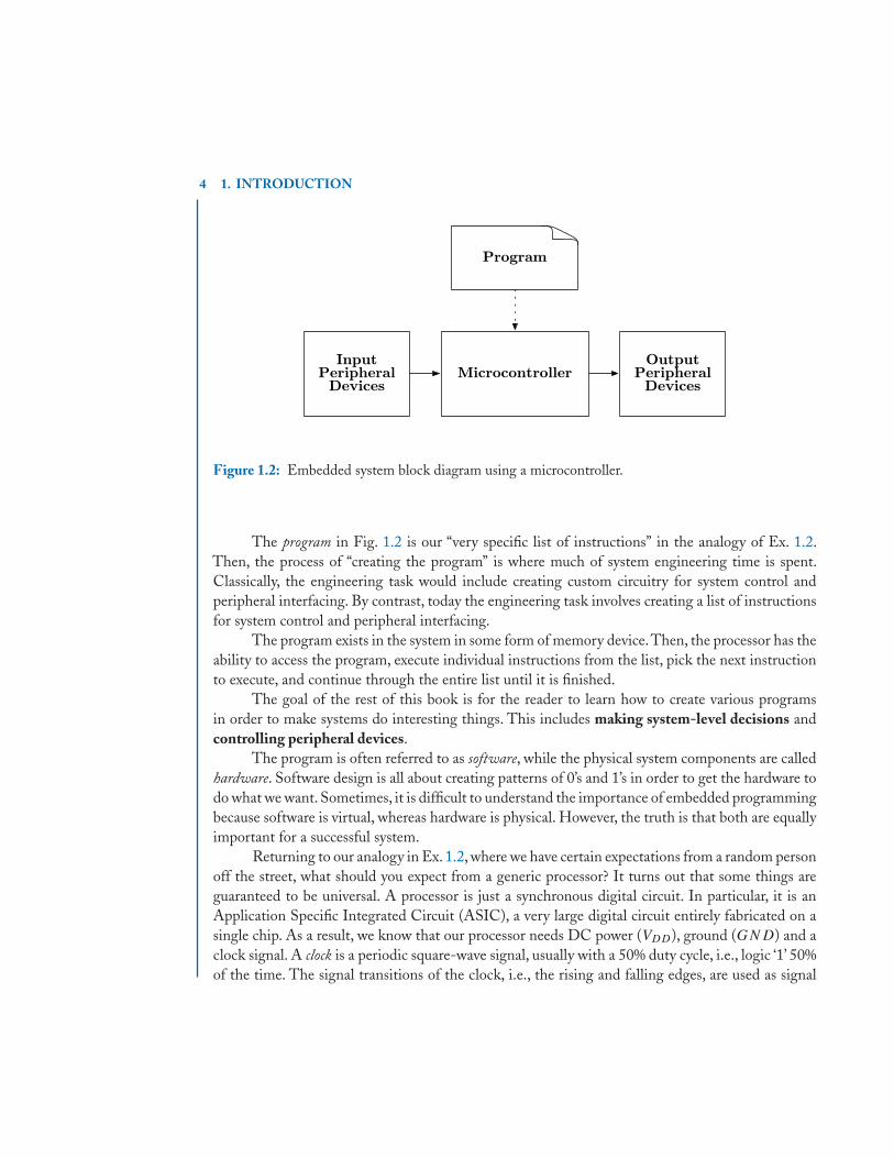
4 1. INTRODUCTION
Input Peripheral Devices
Output Peripheral Devices
Program
Microcontroller
Figure 1.2: Embedded system block diagram using a microcontroller.
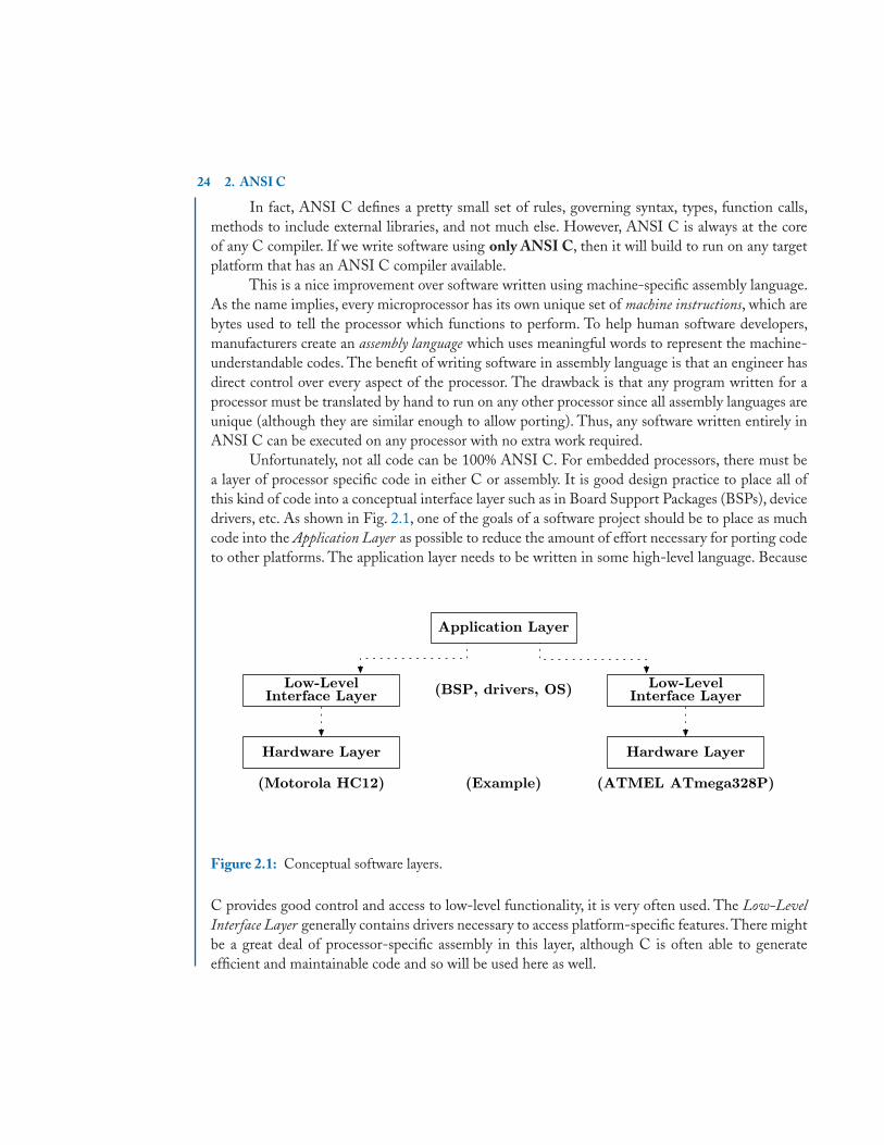
The program in Fig. 1.2 is our “very specific list of instructions” in the analogy of Ex. 1.2.Then, the process of “creating the program” is where much of system engineering time is spent.Classically, the engineering task would include creating custom circuitry for system control andperipheral interfacing. By contrast, today the engineering task involves creating a list of instructionsfor system control and peripheral interfacing.
The program exists in the system in some form of memory device.Then, the processor has theability to access the program, execute individual instructions from the list, pick the next instructionto execute, and continue through the entire list until it is finished.
The goal of the rest of this book is for the reader to learn how to create various programsin order to make systems do interesting things. This includes making system-level decisions andcontrolling peripheral devices.
The program is often referred to as software, while the physical system components are calledhardware. Software design is all about creating patterns of 0’s and 1’s in order to get the hardware todo what we want. Sometimes, it is difficult to understand the importance of embedded programmingbecause software is virtual, whereas hardware is physical. However, the truth is that both are equallyimportant for a successful system.
Returning to our analogy in Ex. 1.2, where we have certain expectations from a random personoff the street, what should you expect from a generic processor? It turns out that some things areguaranteed to be universal. A processor is just a synchronous digital circuit. In particular, it is anApplication Specific Integrated Circuit (ASIC), a very large digital circuit entirely fabricated on asingle chip. As a result, we know that our processor needs DC power (VDD), ground (GND) and aclock signal. A clock is a periodic square-wave signal, usually with a 50% duty cycle, i.e., logic ‘1’ 50%of the time. The signal transitions of the clock, i.e., the rising and falling edges, are used as signal

1.2. DIGITAL REPRESENTATION OF INFORMATION 5
events so that all system components will perform actions at the same time. In other words, they aresynchronized to the clock.
We also know that a processor contains a custom instruction decoder sub-circuit that takesas input some single “instruction” and outputs a signal or set of signals that go to other circuitsub-systems within the microctonroller, telling them to perform some function. This is the heart ofthe processor, and it is the bulk of the Central Processing Unit (CPU ). Because this is just a customdecoder circuit, instructions valid for processor A are likely completely different for processor B.That is, the machine language is unique for every processor.
Along with the CPU,there is an Arithmetic/Logic Unit (ALU ) that is responsible for perform-ing all of the standard operations such as addition, subtraction, multiplication, etc. Each operationtakes in its operands from values stored in CPU registers, which are small groups of memory used bythe ALU and CPU.
Finally, every processor has access to two conceptual banks of memory. Non-volatile memoryholds the program, kind of like a textbook, while volatile memory provides the CPU the freedom torun the program, kind of like scratch paper.
Just as there are common components and features that you can expect out of every micro-controller, there are also common questions that arise at the beginning of every project based on anew component. We need to know the power supply requirement, maximum clock frequency whichdetermines how fast a single instruction can be executed, the machine language, the capabilities ofthe ALU, the number and size of the CPU registers, how instructions interact with the registers,how much memory is available, etc.
All relevant processor information is found in a document provided by the manufacturercalled a data sheet or reference manual. It includes physical characteristics including the packagedimensions and operating properties such as temperature effects. It also includes specific detailsregarding various components/features/blocks of the component such on-board peripherals, internalmemory, maximum clock frequency, number and size of registers, etc. It also includes the instructionset on how to control and/or interact with the component.
We will refer to the ATMEL ATmega328P data sheet throughout the book to learn howvarious aspects of our specific microcontroller works. In particular, whenever necessary, the relevantfeatures, register addresses and meanings will be provided within the respective section.
1.2 DIGITAL REPRESENTATION OF INFORMATION
Most computers are digital, being constructed out of digital circuits. Voltage levels are used torepresent the binary symbols ‘0’ and ‘1’. Often, GND =‘0’ and VDD =‘1’. Because voltage is ananalog measure, some threshold is set such that if x < T , then we have a ‘0’ and if x > T , then wehave a ‘1’. The choice of T is such that the largest amount of noise is tolerated; this is called the noisemargin.
The CPU is simply a large digital circuit. It operates on digital inputs and produces digitaloutputs. Each individual input/output signal is either a ‘0’ or a ‘1’. Notice these are the two elements
6 1. INTRODUCTION
that make up the set of integers in base-2, also called binary. And so, ‘0’ and ‘1’ are BInary digiTS(BITS – a term coined by C. E. Shannon as a unit of measure for information content).
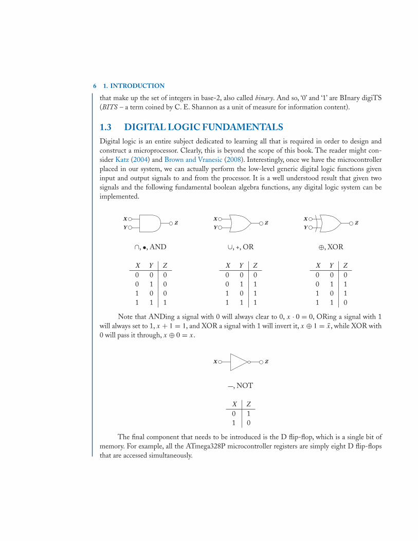
1.3 DIGITAL LOGIC FUNDAMENTALSDigital logic is an entire subject dedicated to learning all that is required in order to design andconstruct a microprocessor. Clearly, this is beyond the scope of this book. The reader might con-sider Katz (2004) and Brown and Vranesic (2008). Interestingly, once we have the microcontrollerplaced in our system, we can actually perform the low-level generic digital logic functions giveninput and output signals to and from the processor. It is a well understood result that given twosignals and the following fundamental boolean algebra functions, any digital logic system can beimplemented.
X
YZ
X
YZ
X
YZ
∩, •, AND ∪, +, OR ⊕, XOR
X Y Z
0 0 00 1 01 0 01 1 1
X Y Z
0 0 00 1 11 0 11 1 1
X Y Z
0 0 00 1 11 0 11 1 0
Note that ANDing a signal with 0 will always clear to 0, x · 0 = 0, ORing a signal with 1will always set to 1, x + 1 = 1, and XOR a signal with 1 will invert it, x ⊕ 1 = x̄, while XOR with0 will pass it through, x ⊕ 0 = x.
X Z
, NOT
X Z
0 11 0
The final component that needs to be introduced is the D flip-flop, which is a single bit ofmemory. For example, all the ATmega328P microcontroller registers are simply eight D flip-flopsthat are accessed simultaneously.
1.4. DIGITAL VECTORS 7
D Q
D Q Q+0 0 00 1 01 0 11 1 1
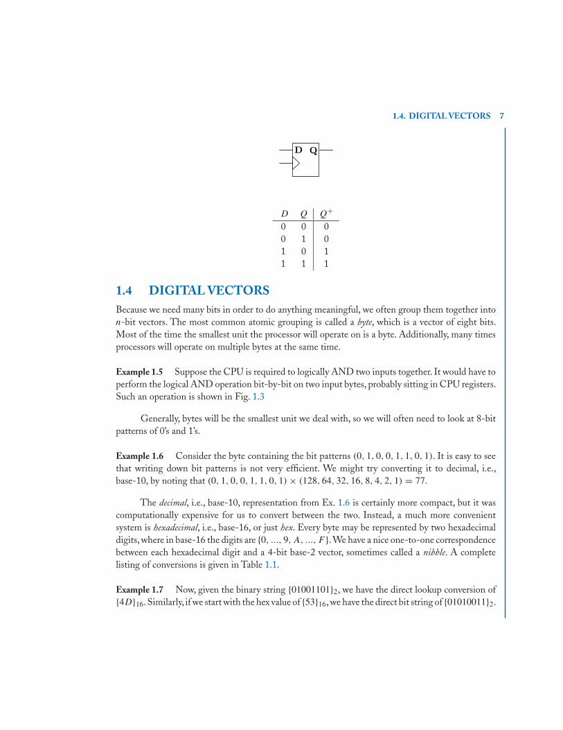
1.4 DIGITAL VECTORSBecause we need many bits in order to do anything meaningful, we often group them together inton-bit vectors. The most common atomic grouping is called a byte, which is a vector of eight bits.Most of the time the smallest unit the processor will operate on is a byte. Additionally, many timesprocessors will operate on multiple bytes at the same time.
Example 1.5 Suppose the CPU is required to logically AND two inputs together. It would have toperform the logical AND operation bit-by-bit on two input bytes, probably sitting in CPU registers.Such an operation is shown in Fig. 1.3
Generally, bytes will be the smallest unit we deal with, so we will often need to look at 8-bitpatterns of 0’s and 1’s.
Example 1.6 Consider the byte containing the bit patterns (0, 1, 0, 0, 1, 1, 0, 1). It is easy to seethat writing down bit patterns is not very efficient. We might try converting it to decimal, i.e.,base-10, by noting that (0, 1, 0, 0, 1, 1, 0, 1) × (128, 64, 32, 16, 8, 4, 2, 1) = 77.
The decimal, i.e., base-10, representation from Ex. 1.6 is certainly more compact, but it wascomputationally expensive for us to convert between the two. Instead, a much more convenientsystem is hexadecimal, i.e., base-16, or just hex. Every byte may be represented by two hexadecimaldigits, where in base-16 the digits are {0, ..., 9, A, ..., F }.We have a nice one-to-one correspondencebetween each hexadecimal digit and a 4-bit base-2 vector, sometimes called a nibble. A completelisting of conversions is given in Table 1.1.
Example 1.7 Now, given the binary string {01001101}2, we have the direct lookup conversion of{4D}16.Similarly, if we start with the hex value of {53}16,we have the direct bit string of {01010011}2.

8 1. INTRODUCTION
c4c5c6c7 c0c1c2c3 b4b5b6b7 b0b1b2b3
d4d5d6d7 d0d1d2d3
Figure 1.3: Logical AND of input signals via the ANDing of two 8-bit vectors. This is required sincethe CPU generally can’t access individual bits – the smallest unit in most CPUs is an 8-bit byte.
Table 1.1: Binary to Hexadecimal ConversionsBase Base Base Base
2 10 16 2 10 16 2 10 16 2 10 160000 0 0 0100 4 4 1000 8 8 1100 12 C0001 1 1 0101 5 5 1001 9 9 1101 13 D0010 2 2 0110 6 6 1010 10 A 1110 14 E0011 3 3 0111 7 7 1011 11 B 1111 15 F
Note that we must be careful about which base we are in.
Example 1.8 What is 101? This can mean two different things depending of in we are in base-2 orbase-16, or base-10 for that matter. If we explicitly qualify {101}2 = {5}10 = {5}16, but {101}10 ={1100101}2 = {65}16.
The numbers presented in Ex. 1.7 and Ex. 1.8 are clearly presented by adding the extra baseidentifier. In programming, these identifiers are replaced by the prefix notations 0x for hex values,and numbers without any marking are identified as decimal. Typically, binary strings are not statedin favor of the more compressed hex representation.

1.5. INFORMATION REPRESENTATION IN A DIGITAL PROCESSOR 9
1.5 INFORMATION REPRESENTATION IN A DIGITALPROCESSOR
1.5.1 NUMBERS1.5.1.1 Unsigned IntegersAll bits of an n-bit binary string are used to represent the inclusion or exclusion of a power of 2. Thebase-10 positive integer is represented via the string (bn−1, ..., b1, b0), which is interpreted as
{N}10 =n−1∑i=0
(bi · 2i
). (1.1)
Example 1.9 A typical byte has n = 8. Suppose {N}2 = (10011100), then
{N}10 = 0 · 20
+ 0 · 21
+ 1 · 22
+ 1 · 23
+ 1 · 24
+ 0 · 25
+ 0 · 26
+ 1 · 27
= (4 + 8 + 16 + 128) = 156
For n-bit bytes, we are able to represent any integer in the range {0, ..., 2n − 1}.Example 1.10 A typical byte has n = 8, which implies the range of values representable is{0, ..., 255}. Other likely values of n are 16 and 32, which have ranges of {0, ..., 65, 535} and{0, ..., 4, 294, 967, 295}, respectively.
Note that we have implied a bit ordering in our definition of the bit string. We have placed themost significant bit (MSB) as the first element of the bit vector and the least significant bit (LSB)as the last element of the vector. This is called big-endian bit format. However, some manufacturerswill reverse this order such that (b0, ..., bn−1), which is called little-endian. Either format is fine, aslong as the reader is aware of the notation. We will use big-endian in this text, which follows theATMEL ATmega328P reference manual as well.
Example 1.11 Suppose you are given {N}2 = (00100110) but not told the order. The meaning ofthe bit string could be either Nbig-endian = 32 or Nlittle-endian = 100. Clearly, it is important to knowthe bit-endianness.
10 1. INTRODUCTION
1.5.1.2 Signed IntegersSometimes, there is a need for the ability to represent negative integer values. To do so, we needto use one of the bits in the string as a flag to indicate when a number is meant as a positive or anegative integer. This bit is called the sign bit, and it is usually the MSB. Let bn−1 = s, and then ifs = 0 then N > 0 or if s = 1 then N < 0.
Example 1.12 Let n = 8. The representation for 77 and -77 are
sign magnitude77 = 0 1001101
-77 = 1 1001101
Here the sign of the number is determined by the MSB sign bit, and the magnitude iscalculated by Eq. (1.1).
In this code,out of n-bits,we have n − 1 bits for the magnitude and 1 bit for the sign indication.Forn-bit bytes,we are able to represent any integer in the range {−2n−1 + 1, ..., −0, 0, ..., 2n−1 − 1}.
Example 1.13 A typical byte has n = 8, which implies the range of values representable is{−127, −0, 0, ..., 127}.
This signed-integer code is called Sign and Magnitude. Its two problems include two versionsof zero, i.e., (10...0) and (00...0) are both mathematically equal to zero in base-10, and the hardwarerequired to perform arithmetic in the ALU is complex, large, slow, etc. Addition of two positive ornegative numbers in sign and magnitude is performed by adding the magnitude bits and using thesign bit of both numbers, as they are the same. Addition of a positive and negative number is a littlemore complicated.
1. Compare the magnitudes. The number with the largest magnitude is placed on top.
2. Perform binary subtraction, i.e., borrowing from the next bit position, etc.
3. The resulting sign bit is the same as the top number.
So, the hardware necessary in an ALU would include a magnitude comparator, an unsigned adder andan unsigned subtractor. These issues have led to more complicated codes for humans to understanddirectly.
First, consider the code called Ones’ Complement in which the magnitude is interpreted as afunction of the sign bit. In other words, the base-10 value is found as follows. As in the previouscode, let bn−1 = s then
{N}10 ={∑n−1
i=0 bi · 2i if s = 0
− ∑n−1i=0 b̄i · 2i if s = 1
(1.2)

1.5. INFORMATION REPRESENTATION IN A DIGITAL PROCESSOR 11
So, the magnitude of the number is calculated after the sign-bit is checked. If the number is positive,the magnitude is as in Eq. (1.1). If the number is negative, the bits are all inverted before themagnitude is calculated with the same equation as before.
Example 1.14 Let n = 8. The representation for 77 is (01001101), just like before. To get -77 inthe ones’ complement code, we negate the number, which means we simply invert all the bits, so(10110010).
Example 1.15 Let n = 8.What do the bit strings (00110111) and (11100110) mean if we interpretthem using ones’ complement? First, look at the sign bit. The first string has a ‘0’, so we know it isa positive number. To calculate its magnitude, we just interpret the bits like we did by Eq. (1.1). So,(00110111) = 55. The second string has a ‘1’, so we know it is a negative number. To calculate itsmagnitude by Eq. (1.2), we need to invert the bits before we add the powers-of-2. So,
(11100110) ⇒ −(00011001) ⇒ −25
which means (11100110) = −25 in ones’ complement.
In this code,out of n-bits,we have n − 1 bits for the magnitude and 1 bit for the sign indication.Forn-bit bytes,we are able to represent any integer in the range {−2n−1 + 1, ..., −0, 0, ..., 2n−1 − 1}.Example 1.16 A typical byte has n = 8, which implies the range of values representable is{−127, −0, 0, ..., 127}.
It turns out the ones’ complement code has solved the issue of hardware complexity in theALU. In particular, performing addition and subtraction on ones’ complement bit strings can be donevia unsigned adder hardware. What this means is that the ALU of a microcontroller can implementa single piece of adder/subtractor hardware and still be able to solve addition and subtraction onboth unsigned and signed integers. Addition of any two numbers in ones’ complement is as follows:
1. Perform binary addition of all bits, including the sign bit.
2. If a ‘1’ is carried out, add it back to the result.
Subtraction of any two numbers in ones’ complement is handled by negating one of the numbersand performing addition.
You may have noticed that ones’ complement still suffers from having two versions of zero.To correct this, consider the code called Two’s Complement in which, just like the ones’ complementcode, the magnitude is interpreted as a function of the sign bit. In other words, the base-10 value isfound as in the previous codes, let bn−1 = s and
{N}10 =⎧⎨⎩
∑n−1i=0 bi · 2i if s = 0
−[(∑n−1
i=0 b̄i · 2i)
+ 1]
if s = 1(1.3)

12 1. INTRODUCTION
So, the magnitude of the number is calculated after the sign-bit is checked. If the number is positive,the magnitude is as in Eq. (1.1). If the number is negative, the bits are all inverted before themagnitude is calculated with Eq. (1.1). The result has 1 added to get the final magnitude.
Example 1.17 Let n = 8. The representation for 77 is (01001101), just like in all other cases. Toget -77 in the two’s complement code, we negate the number, which means we invert all the bitsand add 1, so (10110011).
Example 1.18 Let n = 8.What do the bit strings (00110111) and (11100110) mean if we interpretthem using two’s complement? First, look at the sign bit. The first string has a ‘0’, so we know it isa positive number. To calculate its magnitude, we just interpret the bits like we did by Eq. (1.1). So,(00110111) = 55. The second string has a ‘1’, so we know it is a negative number. To calculate itsmagnitude by Eq. (1.3), we need to invert the bits before we add the powers-of-2. Also, we need toadd 1 before applying the minus sign. So,
(11100110) ⇒ −[(00011001) + 1] ⇒ −26
which means (11100110) = −26 in two’s complement.
In this code,out of n-bits we have n − 1 bits for the magnitude and 1 bit for the sign indication.For n-bit bytes, we are able to represent any integer in the range {−2n−1, ..., −1, 0, ..., 2n−1 − 1}.
Example 1.19 A typical byte has n = 8 which implies the range of values representable is{−128, ..., 127}.
Addition of any two numbers in two’s complement is as follows:
1. Perform binary addition of all bits including the sign bit.
2. If a ‘1’ is carried out, discard it.
Subtraction of any two numbers in two’s complement is handled by negating one of the numbersand performing addition.
Note that two’s complement is the only signed integer code that is ever used in practice.The other two codes are always presented in order to show the progression from taking an unsignedbit string and turning it into an implementable signed-integer representation.The two’s complementcode is always assumed in computer architecture for the same reason ones’ complement was a goodimprovement over sign and magnitude; that is, the two’s complement code allows for addition andsubtraction treatment of bit strings as though they were unsigned integers. The code was designedto allow for efficient hardware in an ALU, i.e., the code does not care if human engineering studentsare unable to decipher the meaning of a bit vectors for a homework assignment.

1.5. INFORMATION REPRESENTATION IN A DIGITAL PROCESSOR 13
Note that we must be careful of overflow conditions which occur when not enough bits areavailable to hold the correct meaning of a calculation.
Example 1.20 Consider using an unsigned adder sub-circuit to perform addition on some bitvectors. We will only care about the unsigned and two’s complement contexts. In the following table,each unsigned hardware operation adds the binary strings, and any carry that is output from theMSB stage is discarded. Depending on the context of signed or unsigned, an overflow indicationmay be made. Note that overflow is not the same thing as carry-out of the MSB.
01001101
(1)0001
In the two’s complement context, this is 4 - 3 = 1, which is correct, and there is no arithmeticoverflow in spite of the fact that a ‘1’ was carried out of the adder’s MSB position. However, in thecontext of unsigned integers, the fact that there is carry out of the MSB is an indication that overflowhas occurred, as 4 + 13 �= 1. If we had a fifth bit available for the output of the operation, then wewould not have had overflow since 4 + 13 = 17 which is 10001 in base-2.
Unsigned Add in Hardware Unsigned Two’s ComplementBit String Value Overflow Value Overflow
(0100 + 0011) (0111) 4 + 3 = 7 4 + 3 = 7(0100 + 0101) (1001) 4 + 5 = 9 4 + 5 �= -7 �(1100 + 1101) (1001) 12 + 13 �= 9 � -4 + -3 = -7(1100 + 1011) (0111) 12 + 11 �= 7 � -4 + -5 �= 7 �
1.5.1.3 Floating PointUnlike integers, in which hardware is pretty much all the same across all architectures, floating-pointcodes are not standard. However, the same basic concepts are generally present. In particular, out ofan n-bit number, one bit is required for the sign of the number, m bits are required for the mantissa,and the remaining e bits are used to represent the exponent. The IEEE floating point formats areshown in Fig. 1.4.
It turns out that floating point arithmetic is always very cycle expensive unless the processorhas a floating point unit built into the ALU, which is hardware expensive. To determine the valueof x given a bit string in IEEE single precision, let s be the sign bit, e the eight exponent bits andm the 23-bit mantissa. Then
x = (−1)s ×(
2e−127)
× 1.m (1.4)
Similarly, the value of x given an IEEE double precision bit string is
x = (−1)s ×(
2e−1023)
× 1.m (1.5)

14 1. INTRODUCTION
Sign Exponent(8) Mantissa(23)
b31 b30 b22b23 b0
Sign Exponent(11) Mantissa(52)
b63 b62 b51b52 b0
Double Precision:
Single Precision:
Figure 1.4: The bit fields of single and double precision IEEE floating point representations.
The s in Eq. (1.4) and Eq. (1.5) controls the sign, just like in all the signed integer codes. Theexponent e moves the binary point, the base-2 equivalent to the base-10 decimal point, to either theright or left and the mantissa m contains the numerical information, or precision.
Example 1.21 To understand the binary point, consider the 4-bit vector (1111). In all of the integercodes, we have a binary point that is always implied to the right of the LSB. In particular, 1111.0which is determined to be 23 + 22 + 21 + 20 = 15. Now suppose the binary point is shifted to theleft, we have
1111. = 23 + 22 + 21 + 20 = 15
111.1 = 22 + 21 + 20 + 2−1 = 7.5
11.11 = 21 + 20 + 2−1 + 2−2 = 3.75
1.111 = 20 + 2−1 + 2−2 + 2−3 = 1.875
.1111 = 2−1 + 2−2 + 2−3 + 2−4 = 0.9375
Notice that because all numbers other than 0 always contain at least one 1, floating pointnumbers are usually interpreted such that the leading 1 is assumed, with the mantissa containingthe entire fractional part.
Example 1.22 Consider the following IEEE single precision representations. Notice that theleading 1 is always assumed in Eq. (1.4). As a result, there is a special check if all bits are 0 torepresent 0.0.
1.5. INFORMATION REPRESENTATION IN A DIGITAL PROCESSOR 15
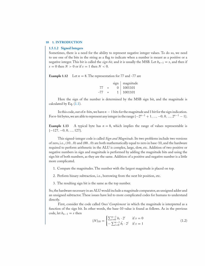
Base-10 Number Sign Exponent Mantissa Value1.0 0 01111111 00000000000000000000000 1.00.5 0 01111110 00000000000000000000000 0.53.5 0 10000000 11000000000000000000000 3.5
largest 0 11111111 11111111111111111111111 6.80564e+38smallest 0 00000000 00000000000000000000001 5.87747e-39
0.0 0 00000000 00000000000000000000000 0.02.44 0 10000000 00111000010100011110101 2.43999
-12.16 1 10000010 10000101000111101011100 -12.15999-9.72 1 10000010 00110111000010100011110 -9.71999
We perform addition just like in base-10.
1. Align the binary points before performing the addition or subtraction. To avoid losing signif-icant digits, the larger number is left alone, and the smaller number has zeros padded in orderto move the binary point into position. In this way, if any precision is lost, it is dropped fromthe smaller number to reduce overall error in the calculation.
2. Addition or subtraction is performed on the aligned magnitudes. This includes the sign ofeach number.
3. The result will have its binary point adjusted to account for any increase or decrease in orderof magnitude.
z =
⎧⎪⎨⎪⎩
[(−1sx × 1.mx) + (−1sy × 1.my × 2−(ex−ey)
)] × 2(ex−127) if |x| ≥ |y|[(−1sy × 1.my
) + (−1sx × 1.mx × 2−(ey−ex))] × 2(ey−127) if |x| ≤ |y|
(1.6)
Example 1.23 Let x = 2.44 and y = −12.16. These numbers can be broken down into theircomponents, so that
x = 2.44
= −10 × 2(128−127) × 1.22= (0, 10000000, 00111000010100011110101)
and
y = −12.16
= −11 × 2(130−127) × 1.52= (1, 10000010, 10000101000111101011100)

16 1. INTRODUCTION
Note that the leading 1 is always assumed, so the mantissa represent 0.22 and 0.52. Now, since|y| > |x|, we calculate the sum as
z =[(
−11 × 1.52)
+(−10 × 1.22 × 2−(130−128)
)]× 2(130−127)
=[(−1 × 1.52) +
(1.22 × 2−2
)]× 23
= [(−1 × 1.52) + (0.305)] × 23
= [−1 × 1.215] × 23
= −9.72
= −11 × 2(130−127) × 1.215= (1, 10000010, 00110111000010100011110)
Clearly there are more steps involved in performing floating point addition as compared tointeger addition.
Single precision floating point multiplication is performed via the equation
z = (−1sx × 1.mx
) × (−1sy × 1.my
) × 2(ex+ey−254) (1.7)
Example 1.24 Let x = 2.44 and y = −12.16, as in Ex. 1.23. We calculate the product as
z =(−11 × 1.52
)×
(−10 × 1.22
)× 2(130+128−254)
= −1 × 1.8544 × 24
= −29.6704
= −11 × 2(131−127) × 1.8544= (1, 10000011, 11011010101110011111010)
The result you should take away from this section is that floating point arithmetic can beimplemented either in hardware or in software on a fixed point processor. For most microproces-sors, the ALU is fixed-point only, so the program written needs to implement all the binary pointadjustments similar to Ex. 1.23 and Ex. 1.24.This is considered cycle expensive since it takes a lot ofinstructions to tell the processor how to perform a single arithmetic operation. So, most embeddedapplications should try to stick with integer arithmetic whenever possible.
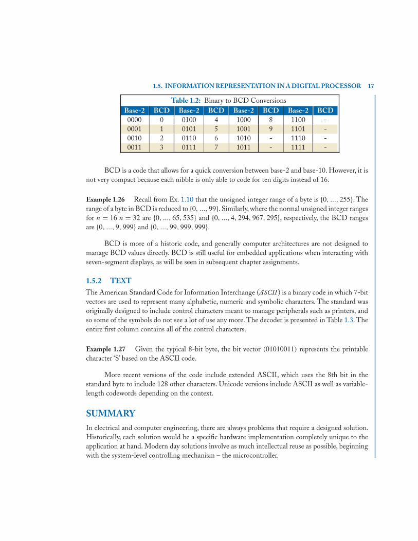
1.5.1.4 Binary Coded DecimalBinary Coded Decimal (BCD) is a special code used to allow direct conversion between a nibble ofbits and a positive decimal value. The binary to BCD conversion is presented in Table 1.2.
Example 1.25 The number {53}10 is represented as the bit vector {01010011}BCD in BCD.
1.5. INFORMATION REPRESENTATION IN A DIGITAL PROCESSOR 17
Table 1.2: Binary to BCD ConversionsBase-2 BCD Base-2 BCD Base-2 BCD Base-2 BCD0000 0 0100 4 1000 8 1100 -0001 1 0101 5 1001 9 1101 -0010 2 0110 6 1010 - 1110 -0011 3 0111 7 1011 - 1111 -
BCD is a code that allows for a quick conversion between base-2 and base-10. However, it isnot very compact because each nibble is only able to code for ten digits instead of 16.
Example 1.26 Recall from Ex. 1.10 that the unsigned integer range of a byte is {0, ..., 255}. Therange of a byte in BCD is reduced to {0, ..., 99}. Similarly, where the normal unsigned integer rangesfor n = 16 n = 32 are {0, ..., 65, 535} and {0, ..., 4, 294, 967, 295}, respectively, the BCD rangesare {0, ..., 9, 999} and {0, ..., 99, 999, 999}.
BCD is more of a historic code, and generally computer architectures are not designed tomanage BCD values directly. BCD is still useful for embedded applications when interacting withseven-segment displays, as will be seen in subsequent chapter assignments.
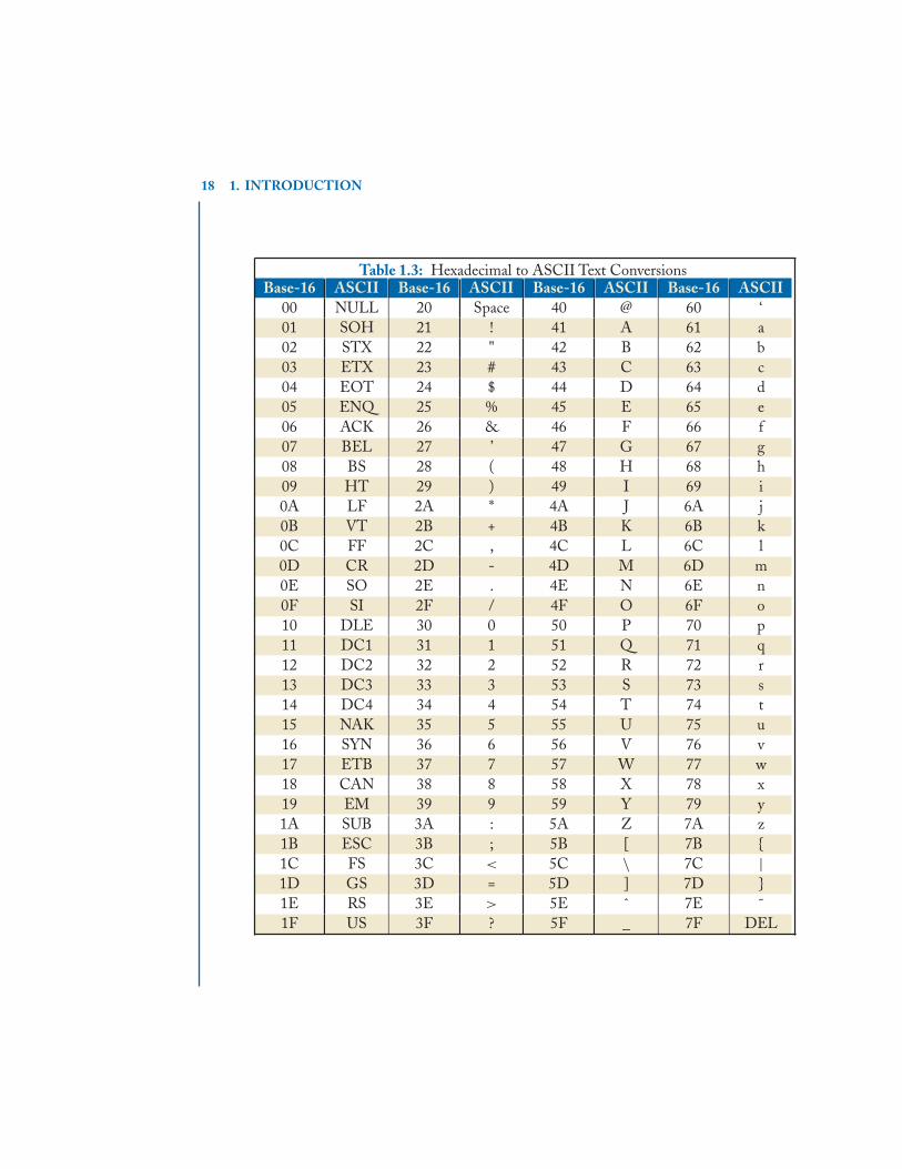
1.5.2 TEXTThe American Standard Code for Information Interchange (ASCII ) is a binary code in which 7-bitvectors are used to represent many alphabetic, numeric and symbolic characters. The standard wasoriginally designed to include control characters meant to manage peripherals such as printers, andso some of the symbols do not see a lot of use any more. The decoder is presented in Table 1.3. Theentire first column contains all of the control characters.
Example 1.27 Given the typical 8-bit byte, the bit vector (01010011) represents the printablecharacter ‘S’ based on the ASCII code.
More recent versions of the code include extended ASCII, which uses the 8th bit in thestandard byte to include 128 other characters. Unicode versions include ASCII as well as variable-length codewords depending on the context.
SUMMARYIn electrical and computer engineering, there are always problems that require a designed solution.Historically, each solution would be a specific hardware implementation completely unique to theapplication at hand. Modern day solutions involve as much intellectual reuse as possible, beginningwith the system-level controlling mechanism – the microcontroller.
18 1. INTRODUCTION
Table 1.3: Hexadecimal to ASCII Text ConversionsBase-16 ASCII Base-16 ASCII Base-16 ASCII Base-16 ASCII
00 NULL 20 Space 40 @ 60 ‘01 SOH 21 ! 41 A 61 a02 STX 22 " 42 B 62 b03 ETX 23 # 43 C 63 c04 EOT 24 $ 44 D 64 d05 ENQ 25 % 45 E 65 e06 ACK 26 & 46 F 66 f07 BEL 27 ’ 47 G 67 g08 BS 28 ( 48 H 68 h09 HT 29 ) 49 I 69 i0A LF 2A * 4A J 6A j0B VT 2B + 4B K 6B k0C FF 2C , 4C L 6C l0D CR 2D - 4D M 6D m0E SO 2E . 4E N 6E n0F SI 2F / 4F O 6F o10 DLE 30 0 50 P 70 p11 DC1 31 1 51 Q 71 q12 DC2 32 2 52 R 72 r13 DC3 33 3 53 S 73 s14 DC4 34 4 54 T 74 t15 NAK 35 5 55 U 75 u16 SYN 36 6 56 V 76 v17 ETB 37 7 57 W 77 w18 CAN 38 8 58 X 78 x19 EM 39 9 59 Y 79 y1A SUB 3A : 5A Z 7A z1B ESC 3B ; 5B [ 7B {1C FS 3C < 5C \ 7C |1D GS 3D = 5D ] 7D }1E RS 3E > 5E ˆ 7E ˜1F US 3F ? 5F _ 7F DEL

1.5. INFORMATION REPRESENTATION IN A DIGITAL PROCESSOR 19
With an embedded processor at the heart of each system, both electrical engineering andcomputer science concepts are essential to creating a sound design. We began with the concept ofusing analog voltage levels to represent discrete binary values ‘0’ and ‘1’, which are also the symbols ofthe binary number system.As a result, all the concepts present in Boolean Algebra are also available inhardware and software development in the form of digital logic. A few fundamental logic operationsprovide the basis for building large circuits of logic.
Because base-2 is all we can implement in hardware directly, we introduce several codingschemes used to represent other number systems given multidimensional vectors of 0’a and 1’s.Among these are the systems for representing unsigned integers, signed integers, floating-pointnumbers (i.e., the reals), and printable text characters. We complete this chapter with one finalexample to convey the following important concept: the only real thing in a microcontroller arethe voltages used to represent individual bits; how we interpret those strings of bits is completelybased on a higher-level context.
Example 1.28 Suppose we want to store the information {123}10.We can do so using the followingbit strings when interpreted with the associated context. Unsigned is 01111011, two’s complement is01111011, BCD is 0001, 0010, 0011 and ASCII is 00110001, 00110010, 00110011. Next, considerthe information {−12}10. Neither unsigned nor BCD codes are able to store this information. Two’scomplement is 11110100 and ASCII is 00101101, 00110001, 00110010.
The importance of this example is that any string of bits may exist in our processor. Themeaning of the bits is dependent on the context being used to interpret the bit vector.
PROBLEMS1.1 Given a digital system with VDD = 5V, what analog-to-digital threshold T should be selected
to maximize the noise margins. You should assume an ideal model where x < T ⇒ 0 andx > T ⇒ 1.
1.2 Given a digital system with VDD = 1.8V, and an analog-to-digital threshold T = 1.0V suchthat x < T ⇒ 0 and x > T ⇒ 1. Sketch the input/output relationship for 0 ≤ Vin ≤ 1.8Vwhere Vout = 0V for ‘0’ and Vout = 1.8V for ‘1’.
1.3 Given the system in problem 1.2, state the bit that is mapped to from each voltage.
(a) 0.1V
(b) 1.73267589V
(c) 0.99V
(d) 1.01V
1.4 Given the system in problem 1.2, state how much analog voltage noise can be tolerated onboth the low and high logic levels.
20 1. INTRODUCTION
1.5 Given {01110110110100011001101111110000}2, determine the equivalent number in eachbase.
(a) Decimal
(b) Hexadecimal
1.6 Given {24687531}16, determine the equivalent number in each base.
(a) Decimal
(b) Binary
1.7 Given {24687531}10, determine the equivalent number in each base.
(a) Hexadecimal
(b) Binary
1.8 Using 8-bit bytes, show how to represent 123. Clearly state the byte values using hexadecimal,and the number of bytes required for each context. Simply indicate the case if the code is notable to represent the information.
(a) Unsigned integer
(b) Two’s complement
(c) BCD
(d) ASCII
1.9 Using 8-bit bytes, show how to represent -123. Clearly state the byte values using hexadecimal,and the number of bytes required for each context. Simply indicate the case if the code is notable to represent the information.
(a) Unsigned integer
(b) Two’s complement
(c) BCD
(d) ASCII
1.10 Using 8-bit bytes, show how to represent 56,789. Clearly state the byte values using hexadec-imal, and the number of bytes required for each context. Simply indicate the case if the codeis not able to represent the information.
(a) Unsigned integer
(b) Two’s complement
(c) BCD

1.5. INFORMATION REPRESENTATION IN A DIGITAL PROCESSOR 21
(d) ASCII
(e) IEEE single precision
1.11 Using 8-bit bytes, show how to represent -6,543. Clearly state the byte values using hexadec-imal, and the number of bytes required for each context. Simply indicate the case if the codeis not able to represent the information.
(a) Unsigned integer
(b) Two’s complement
(c) BCD
(d) ASCII
(e) IEEE single precision
1.12 Using 8-bit bytes, show how to represent 1.23456. Clearly state the byte values using hex-adecimal, and the actual number represented with 7 fractional digits.
(a) IEEE single precision
(b) IEEE double precision
1.13 Using 8-bit bytes, show how to represent -65.43210. Clearly state the byte values using hex-adecimal, and the actual number represented with 5 fractional digits.
(a) IEEE single precision
(b) IEEE double precision

23
C H A P T E R 2
ANSI C
2.1 INTRODUCTION
One of the most valuable tools an embedded engineer can have at their disposal is knowledge of theC programming language. So many aspects of the technological industry change within a very shorttime. As a result, it can seem as though many of the industry-standard tools learned in the classroomtoday are obsolete within a few years of obtaining an engineering position. Interestingly, this is nottrue of the C programming language, which was introduced in the 1970’s, and is still the mostoften-used high-level language in embedded systems.This means that even after 40 years, engineersare still able to develop systems using the same reliable tool. This book is really born from the factthat I believe C is a cornerstone for every undergraduate computer and electrical engineer. Onceyou know the material in this chapter, you will be employable regardless of the latest microprocessorlifecycle.
Most information presented within this chapter comes from notes taken fromKernighan and Ritchie (1989). All additional material is provided from personal work experience(14 years and counting).
2.1.1 BACKGROUNDC, influenced from BCPL and B in 1970, is considered a “low-level” high-level language, meaningyou can access anything using C that you can in the platform’s native assembly language. In gen-eral, use of a high-level language reduces the amount of knowledge required about the underlyinghardware architecture.
One of the original uses of C was in the development of the UNIX operating system and var-ious compilers. In 1983, the American National Standards Institute (ANSI) established a definitionof C, which eventually led to ANSI C defined in 1988. As a result, any compiler that claims ANSIcompliance must pass a series of tests. ANSI C is 100% portable code meaning that no matter whatthe target hardware platform is, if the software is written in pure ANSI C then it can be used tocreate an executable program.
Example 2.1 Question: Why can’t Microsoft take Word and just re-compile it to run on MacOSXor Linux? Answer: Aside from various marketing reasons, the software is not pure ANSI C, and soit is not directly portable from one processor to another (or one operating system to another, for thatmatter).
24 2. ANSI C
In fact, ANSI C defines a pretty small set of rules, governing syntax, types, function calls,methods to include external libraries, and not much else. However, ANSI C is always at the coreof any C compiler. If we write software using only ANSI C, then it will build to run on any targetplatform that has an ANSI C compiler available.
This is a nice improvement over software written using machine-specific assembly language.As the name implies, every microprocessor has its own unique set of machine instructions, which arebytes used to tell the processor which functions to perform. To help human software developers,manufacturers create an assembly language which uses meaningful words to represent the machine-understandable codes. The benefit of writing software in assembly language is that an engineer hasdirect control over every aspect of the processor. The drawback is that any program written for aprocessor must be translated by hand to run on any other processor since all assembly languages areunique (although they are similar enough to allow porting). Thus, any software written entirely inANSI C can be executed on any processor with no extra work required.
Unfortunately, not all code can be 100% ANSI C. For embedded processors, there must bea layer of processor specific code in either C or assembly. It is good design practice to place all ofthis kind of code into a conceptual interface layer such as in Board Support Packages (BSPs), devicedrivers, etc. As shown in Fig. 2.1, one of the goals of a software project should be to place as muchcode into the Application Layer as possible to reduce the amount of effort necessary for porting codeto other platforms. The application layer needs to be written in some high-level language. Because
Application Layer
Low-Level Interface Layer
Low-Level Interface Layer(BSP, drivers, OS)
Hardware Layer Hardware Layer
(Motorola HC12) (ATMEL ATmega328P)(Example)
Figure 2.1: Conceptual software layers.
C provides good control and access to low-level functionality, it is very often used. The Low-LevelInterface Layer generally contains drivers necessary to access platform-specific features. There mightbe a great deal of processor-specific assembly in this layer, although C is often able to generateefficient and maintainable code and so will be used here as well.
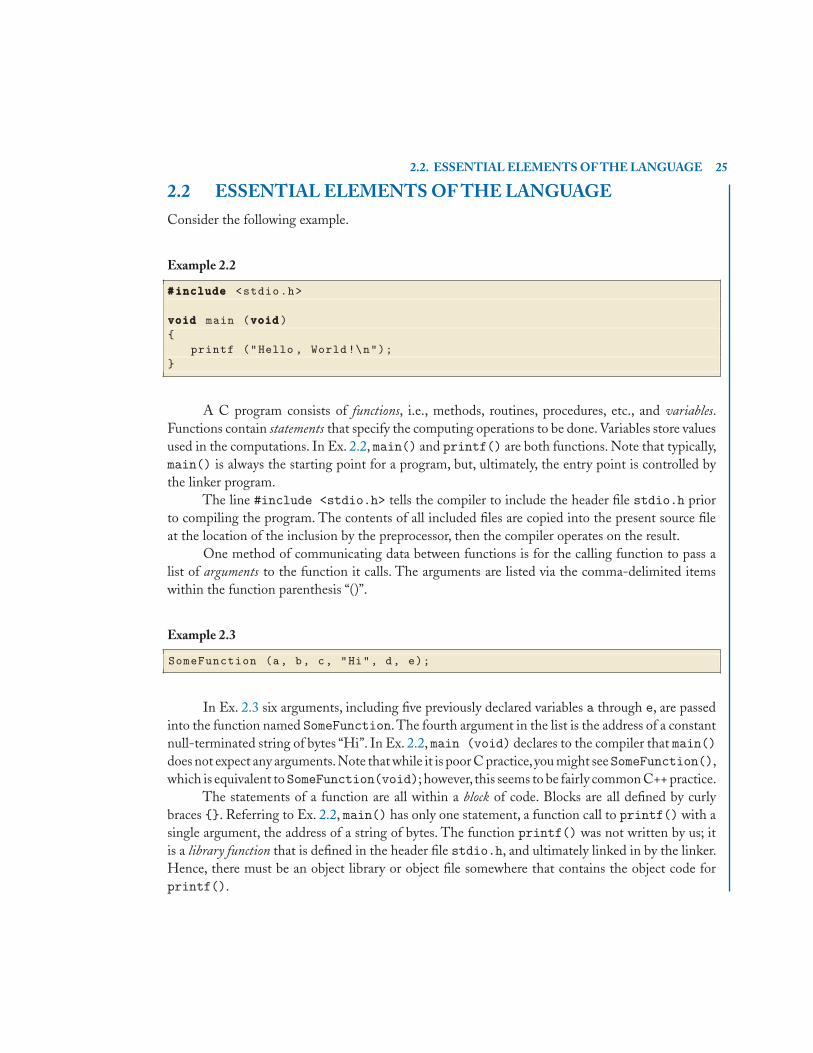
2.2. ESSENTIAL ELEMENTS OF THE LANGUAGE 25
2.2 ESSENTIAL ELEMENTS OF THE LANGUAGEConsider the following example.
Example 2.2
###includeincludeinclude <stdio.h>
voidvoidvoid main (voidvoidvoid){
printf ("Hello , World!\n");}
A C program consists of functions, i.e., methods, routines, procedures, etc., and variables.Functions contain statements that specify the computing operations to be done. Variables store valuesused in the computations. In Ex. 2.2, main() and printf() are both functions. Note that typically,main() is always the starting point for a program, but, ultimately, the entry point is controlled bythe linker program.
The line #include <stdio.h> tells the compiler to include the header file stdio.h priorto compiling the program. The contents of all included files are copied into the present source fileat the location of the inclusion by the preprocessor, then the compiler operates on the result.
One method of communicating data between functions is for the calling function to pass alist of arguments to the function it calls. The arguments are listed via the comma-delimited itemswithin the function parenthesis “()”.
Example 2.3
SomeFunction (a, b, c, "Hi", d, e);
In Ex. 2.3 six arguments, including five previously declared variables a through e, are passedinto the function named SomeFunction.The fourth argument in the list is the address of a constantnull-terminated string of bytes “Hi”. In Ex. 2.2, main (void) declares to the compiler that main()does not expect any arguments.Note that while it is poor C practice,you might seeSomeFunction(),which is equivalent toSomeFunction(void); however, this seems to be fairly common C++ practice.
The statements of a function are all within a block of code. Blocks are all defined by curlybraces {}. Referring to Ex. 2.2, main() has only one statement, a function call to printf() with asingle argument, the address of a string of bytes. The function printf() was not written by us; itis a library function that is defined in the header file stdio.h, and ultimately linked in by the linker.Hence, there must be an object library or object file somewhere that contains the object code forprintf().

26 2. ANSI C
2.3 FORMATTED OUTPUT
Often in embedded environments, we have to rely completely on printf() in order to look atvariable values, which is a fundamental component in the debugging process. The fprintf()function provides formatted output conversion.
Example 2.4
intintint fprintf (FILE *stream , constconstconst charcharchar *format , ...)
This function converts and writes output to stream under the control of format. The returnvalue is the number of characters written, or negative if an error occurred.The format string containstwo types of objects.
1. Ordinary characters, which are copied to the output stream, and
2. conversion specifications, each of which causes conversion and printing of the next successiveargument to fprintf().
Each conversion specification begins with the character % and ends with a conversion character.Between the % and the conversion character there may be, in the following order:
• Flags (in any order), which modify the specification, are listed in Table 2.1.
Table 2.1: Formatted Printing Conversion Specification FlagsFlag Modification- specifies left adjustment of the converted argument in its field+ specifies that the number will always be printed with a sign
space if the first character is not a sign, a space will be prefixed0 for numeric conversion, specifies padding to the field width with leading zeros# specifies an alternative output form
(e.g., for x, 0x will be prefixed to a non-zero result)
• A number specifying a minimum field width.The converted argument will be printed in a fieldat least this wide, and wider if necessary. If the converted argument has fewer characters thanthe field width, it will be padded on the left (or right, if left adjustment has been requested) tomake up the field width. The padding character is normally space, but 0 if the zero paddingflag is present.
• A period, which separates the field width from the precision.

2.3. FORMATTED OUTPUT 27
• A number, the precision, that specifies the maximum number of characters to be printed froma string, or the number of digits to be printed after the decimal point for e or f conversions,or the number of significant digits for g conversion, or the minimum number of digits to beprinted for an integer (leading 0s will be added to make up the necessary width).
• A length modifier h, l or L. h indicates that the corresponding argument is to be printed as ashort or unsigned short; l indicates that the argument is a long or unsigned long; Lindicates that the argument is a long double.
Width or precision or both may be specified as *; in which case, the value is computed by convertingthe next argument(s), which must be int.
Example 2.5
printf ("%.*s", max , theString);
will output at most max characters from theString.
The conversion characters and their interpretations are listed in Table 2.2.
Table 2.2: Formatted Printing Conversion CharactersChar Type Interpretationd,i int signed decimal notationo int unsigned octal notation (without leading 0)x int unsigned hexadecimal notation (without leading 0x, uses abcdef)X int unsigned hexadecimal notation (without leading 0x, uses ABCDEF)u int unsigned decimal notationc int single character, after conversion to unsigned char)s char * characters from the string until a \0 or precision is reached)f double decimal notation of the form [−]mmm.ddd; precision controls dse,E double decimal notation of the form [−]m.ddde±xx; precision controls dsg,G double selects the best choice between %e and %fp void * print as a pointer (implementation-dependent representation)n int * the number of characters output so far via this printf() is
copied into the argument; no argument is converted% print a %; no argument is converted
If the character after the % is not a conversion character, the behavior is undefined. Thecharacter constants and their meanings are listed in Table 2.3.
Other forms of fprintf() include the functions in Ex. 2.6-Ex.2.8.
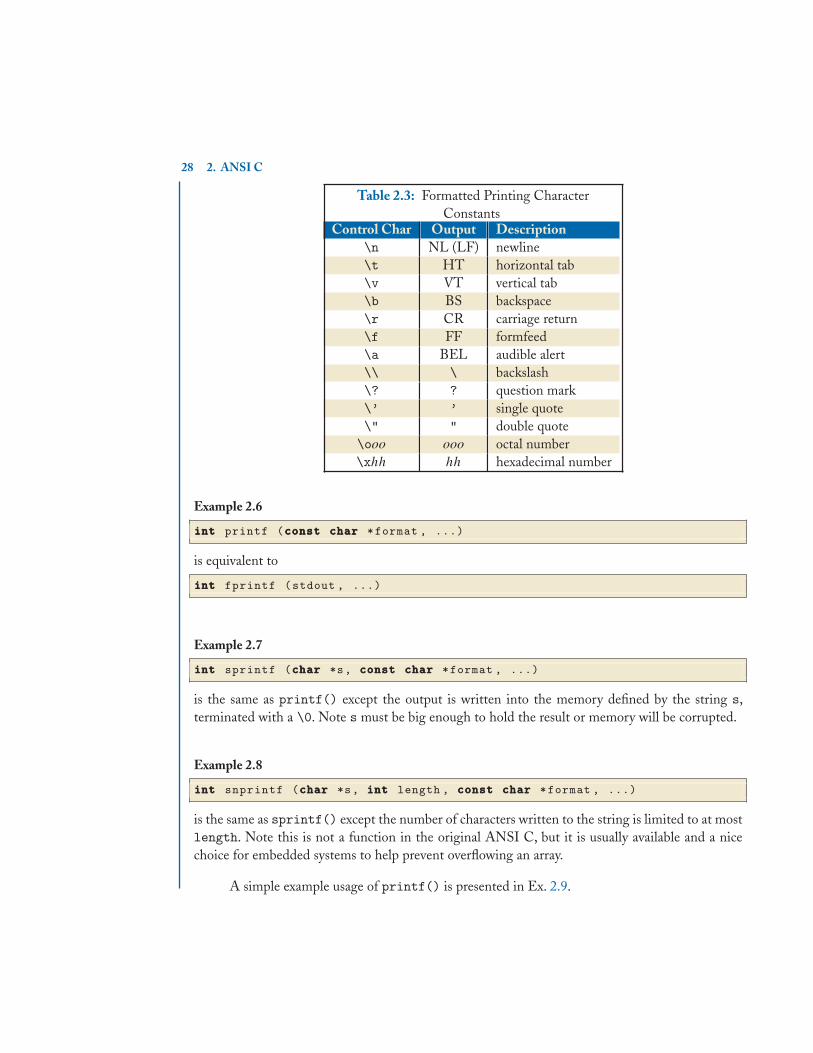
28 2. ANSI C
Table 2.3: Formatted Printing CharacterConstants
Control Char Output Description\n NL (LF) newline\t HT horizontal tab\v VT vertical tab\b BS backspace\r CR carriage return\f FF formfeed\a BEL audible alert\\ \ backslash\? ? question mark\’ ’ single quote\" " double quote\ooo ooo octal number\xhh hh hexadecimal number
Example 2.6
intintint printf (constconstconst charcharchar *format , ...)
is equivalent to
intintint fprintf (stdout , ...)
Example 2.7
intintint sprintf (charcharchar *s, constconstconst charcharchar *format , ...)
is the same as printf() except the output is written into the memory defined by the string s,terminated with a \0. Note s must be big enough to hold the result or memory will be corrupted.
Example 2.8
intintint snprintf (charcharchar *s, intintint length , constconstconst charcharchar *format , ...)
is the same as sprintf() except the number of characters written to the string is limited to at mostlength. Note this is not a function in the original ANSI C, but it is usually available and a nicechoice for embedded systems to help prevent overflowing an array.
A simple example usage of printf() is presented in Ex. 2.9.

2.3. FORMATTED OUTPUT 29
Example 2.9
intintint x = 78;unsignedunsignedunsigned longlonglong y = 93;floatfloatfloat z = 12.34;
printf("variables x = %d, y = %lu and z = %.2f\nnote x = %#2.2x inhex\n", x, y, z, x);
this code would result in the output
variables x = 78, y = 93 and z = 12.34note x = 0x4e in hex
The format string is managed in the following way.
• Characters are simply written out until a % conversion indicator is encountered;
printf("variables x = %d, y = %lu and z = %.2f\nnote x = %#2.2x in hex\n", x, y, z, x);
• When the %d is seen, the first variable after the format string is interpreted as a signed decimalvalue because of the d character conversion code. So 78 is printed out due to the first occurrenceof x;
printf("variables x = %d, y = %lu and z = %.2f\nnote x = %#2.2x in hex\n", x, y, z, x);
• The next characters, y =, are output
printf("variables x = %d, y = %lu and z = %.2f\nnote x = %#2.2x in hex\n", x, y, z, x);
• Until %lu is seen, at which point, the next variable in the argument list is interpreted as a longunsigned decimal value, and 93 is output;
printf("variables x = %d, y = %lu and z = %.2f\nnote x = %#2.2x in hex\n", x, y, z, x);
• This is followed by the output of and z =
printf("variables x = %d, y = %lu and z = %.2f\nnote x = %#2.2x in hex\n", x, y, z, x);
• Until %.2f is seen, at which time, the next variable in the argument list is interpreted as adouble value, and the additional precision restricts the output to 12.34;
printf("variables x = %d, y = %lu and z = %.2f\nnote x = %#2.2x in hex\n", x, y, z, x);
• The next character parsed is the constant \n, which moves to a new line;
printf("variables x = %d, y = %lu and z = %.2f\nnote x = %#2.2x in hex\n", x, y, z, x);
• Which is followed by the next set of characters note x =
printf("variables x = %d, y = %lu and z = %.2f\nnote x = %#2.2x in hex\n", x, y, z, x);

30 2. ANSI C
• Until %#2.2x is seen, where the final variable in the list is interpreted as hexadecimal with awidth and precision of 2 characters, so 0x4e is output. Note the 0x is printed as a result of the# flag in the conversion code;
printf("variables x = %d, y = %lu and z = %.2f\nnote x = %#2.2x in hex\n", x, y, z, x);
• The final part of the format string finishes the example by outputting in hex and a final newline character.
printf("variables x = %d, y = %lu and z = %.2f\nnote x = %#2.2x in hex\n", x, y, z, x);
2.4 VARIABLES AND ARITHMETIC EXPRESSIONSConsider Ex 2.10.
Example 2.10
voidvoidvoid main (voidvoidvoid){
intintint farenheit;intintint celsius;intintint lower;intintint upper;intintint step;
lower = 0; /* lower limit */upper = 300;step = 20;farenheit = lower;whilewhilewhile (farenheit <= upper){
celsius = 5 * (farenheit - 32) / 9;farenheit = farenheit + step;printf ("%d F = %d C\n", farenheit , celsius);
}}
Note that anything between /* and */ are comments, and ignored by the compiler. Addi-tionally, C++ allows for inline comments where anything after // is ignored by the compiler until anew line character. When used properly, comments are useful for generating maintainable software.Comments can contain any prose desired, which allows a developer the ability to document interest-ing aspects of the program. All comments are discarded by the compiler, so their presence is strictlyused for documentation purposes.
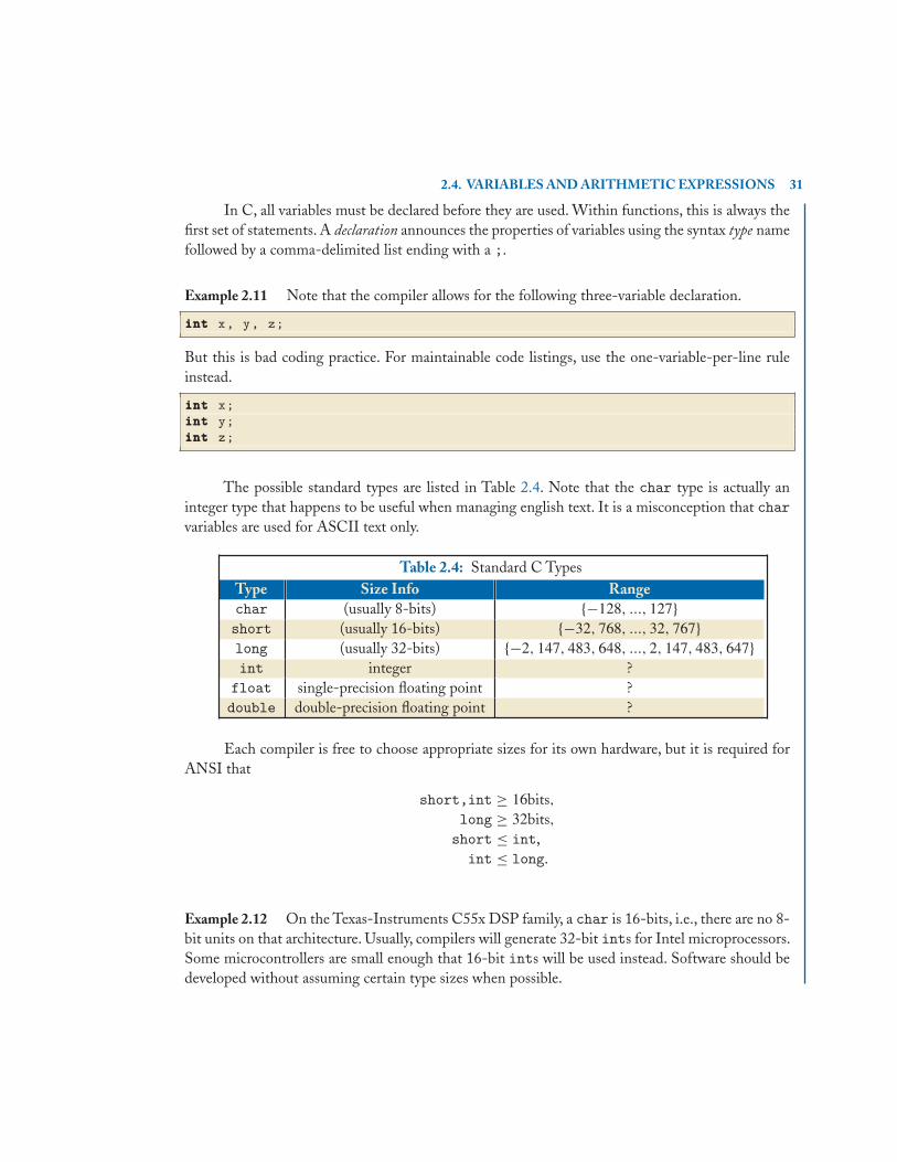
2.4. VARIABLES AND ARITHMETIC EXPRESSIONS 31
In C, all variables must be declared before they are used. Within functions, this is always thefirst set of statements. A declaration announces the properties of variables using the syntax type namefollowed by a comma-delimited list ending with a ;.
Example 2.11 Note that the compiler allows for the following three-variable declaration.
intintint x, y, z;
But this is bad coding practice. For maintainable code listings, use the one-variable-per-line ruleinstead.
intintint x;intintint y;intintint z;
The possible standard types are listed in Table 2.4. Note that the char type is actually aninteger type that happens to be useful when managing english text. It is a misconception that charvariables are used for ASCII text only.
Table 2.4: Standard C TypesType Size Info Rangechar (usually 8-bits) {−128, ..., 127}short (usually 16-bits) {−32, 768, ..., 32, 767}long (usually 32-bits) {−2, 147, 483, 648, ..., 2, 147, 483, 647}int integer ?float single-precision floating point ?double double-precision floating point ?
Each compiler is free to choose appropriate sizes for its own hardware, but it is required forANSI that
short,int ≥ 16bits,long ≥ 32bits,short ≤ int,
int ≤ long.
Example 2.12 On the Texas-Instruments C55x DSP family, a char is 16-bits, i.e., there are no 8-bit units on that architecture. Usually, compilers will generate 32-bit ints for Intel microprocessors.Some microcontrollers are small enough that 16-bit ints will be used instead. Software should bedeveloped without assuming certain type sizes when possible.
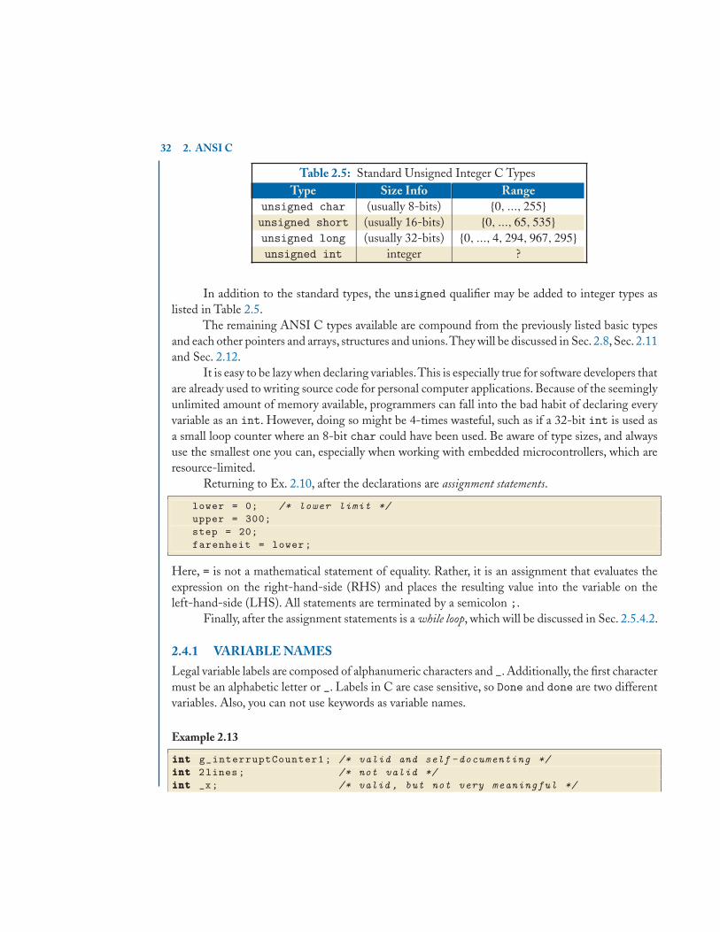
32 2. ANSI C
Table 2.5: Standard Unsigned Integer C TypesType Size Info Range
unsigned char (usually 8-bits) {0, ..., 255}unsigned short (usually 16-bits) {0, ..., 65, 535}unsigned long (usually 32-bits) {0, ..., 4, 294, 967, 295}unsigned int integer ?
In addition to the standard types, the unsigned qualifier may be added to integer types aslisted in Table 2.5.
The remaining ANSI C types available are compound from the previously listed basic typesand each other pointers and arrays, structures and unions.They will be discussed in Sec. 2.8, Sec. 2.11and Sec. 2.12.
It is easy to be lazy when declaring variables.This is especially true for software developers thatare already used to writing source code for personal computer applications. Because of the seeminglyunlimited amount of memory available, programmers can fall into the bad habit of declaring everyvariable as an int. However, doing so might be 4-times wasteful, such as if a 32-bit int is used asa small loop counter where an 8-bit char could have been used. Be aware of type sizes, and alwaysuse the smallest one you can, especially when working with embedded microcontrollers, which areresource-limited.
Returning to Ex. 2.10, after the declarations are assignment statements.
lower = 0; /* lower limit */upper = 300;step = 20;farenheit = lower;
Here, = is not a mathematical statement of equality. Rather, it is an assignment that evaluates theexpression on the right-hand-side (RHS) and places the resulting value into the variable on theleft-hand-side (LHS). All statements are terminated by a semicolon ;.
Finally, after the assignment statements is a while loop, which will be discussed in Sec. 2.5.4.2.
2.4.1 VARIABLE NAMESLegal variable labels are composed of alphanumeric characters and _. Additionally, the first charactermust be an alphabetic letter or _. Labels in C are case sensitive, so Done and done are two differentvariables. Also, you can not use keywords as variable names.
Example 2.13
intintint g_interruptCounter1; /* valid and self -documenting */intintint 2lines; /* not valid */intintint _x; /* valid , but not very meaningful */

2.4. VARIABLES AND ARITHMETIC EXPRESSIONS 33
intintint intintint; /* not valid */intintint floatfloatfloat; /* not valid */intintint ififif; /* not valid */intintint whilewhilewhile; /* not valid */
As an aside, there are varying degrees of quality regarding source-code listings. Consider thelabels used to represent variables and functions. Because the labels can be nearly any combinationof alphanumeric letters, we can generate self-documenting code by using meaningful names. In fact,by using overly descriptive labels, there is no need for comments that tend to fall out-of-sync withthe instructions they attempt to describe.
2.4.2 TYPE CONVERSIONSC allows for assigning variables to each other even of different types. But what about the storagedifference?
Example 2.14
charcharchar c;shortshortshort s;
/* suppose s is assigned some value prior to this assignment */c = s;
/* suppose c is assigned some value prior to this assignment */s = c;
Suppose that in Ex. 2.14 a char variable is 8 bits and a short variable is 16 bits. Then theassignment s = c poses no problem; the extra bits are simply sign-extended as shown in Fig. 2.2.To understand why sign-extension works (or is needed), first consider the case when c = 1 which is
s10s11s12s13s14s15 s4s5s6s7s8s9 s0s1s2s3
c4c5c6c7 c0c1c2c3
Figure 2.2: An 8-bit signed integer value is loaded into a 16-bit storage location. The correct two’scomplement value is generated by performing sign extension.

34 2. ANSI C
stored as{c}2 = (0, 0, 0, 0, 0, 0, 0, 1).
As the figure implies, the first step is copying the bits from c into the lower 8 bits of s,
{s}2 = (x, x, x, x, x, x, x, x, 0, 0, 0, 0, 0, 0, 0, 1).
Then, for s to hold the correct value of s = 1, the sign-bit of c7 = 0 is copied into the upper 8 bitsof s resulting in
{s}2 = (0, 0, 0, 0, 0, 0, 0, 0, 0, 0, 0, 0, 0, 0, 0, 1),
or s = 1 as required. Now consider the case when c = −1 which is stored in two’s complement as
{c}2 = (1, 1, 1, 1, 1, 1, 1, 1)
(remember, two’s complement negation is found via the “invert and add 1” process). Following thesame process in the figure, the bits are copied from c into the lower 8 bits of s,
{s}2 = (x, x, x, x, x, x, x, x, 1, 1, 1, 1, 1, 1, 1, 1).
Now, for s to hold the correct value of s = −1, the sign-bit of c7 = 1 is copied into the upper 8 bitsof s resulting in
{s}2 = (1, 1, 1, 1, 1, 1, 1, 1, 1, 1, 1, 1, 1, 1, 1, 1)
which is the correct two’s complement representation for s = −1.Alternatively, the assignment c = s as shown in Fig. 2.3. In this case, the destination doesn’t
s10s11s12s13s14s15 s4s5s6s7s8s9 s0s1s2s3
c4c5c6c7 c0c1c2c3‘‘Bit Bucket’’
Figure 2.3: A 16-bit signed integer value is loaded into an 8-bit storage location.The final value is forcedto ignore the upper 8-bit values of the source.
have enough room to hold the entire source value. As a result, the lower 8 bits of s are copied intoc and the higher 8 bits of s are discarded into the “bit bucket” virtual trash can. If any of the upper8 bits contain information necessary for the correct meaning of the value stored in the variable, thenoverflow (OV) occurs. Overflow happens any time the destination variable does not have enoughroom to contain the true meaning of the information being loaded.
Example 2.15 Consider the following assignments between an 8-bit, signed integer char c anda 16-bit, signed integer short s.

2.4. VARIABLES AND ARITHMETIC EXPRESSIONS 35
Source DestinationAssignment Base-10 Base-2 Base-10 Base-2 OV
c = s 123 (0000, 0000, 0111, 1011) 123 (0111, 1011)
s = c 123 (0111, 1011) 123 (0000, 0000, 0111, 1011)
c = s 145 (0000, 0000, 1001, 0001) -111 (1001, 0001) �s = c -111 (1001, 0001) -111 (1111, 1111, 1001, 0001)
c = s 9780 (0010, 0110, 0011, 0100) 52 (0011, 0100) �
Next, consider how unsigned integer variables are assigned between different sized types.
Example 2.16
unsignedunsignedunsigned charcharchar c;unsignedunsignedunsigned shortshortshort s;
/* suppose s is assigned some value prior to this assignment */c = s;
/* suppose c is assigned some value prior to this assignment */s = c;
Suppose that variables in Ex. 2.16 use the same number of bits as those from Ex. 2.14. As inthe signed case, the assignment s = c poses no problem; the extra bits are cleared to zero as shownin Fig. 2.4. By clearing the upper 8 bits, it is guaranteed that the destination will always be a positive
s10s11s12s13s14s15 s4s5s6s7s8s9 s0s1s2s3
c4c5c6c7 c0c1c2c3
00000000
Figure 2.4: An 8-bit unsigned integer value is loaded into a 16-bit storage location.The correct unsignedvalue is generated by clearing the most significant bits to zero.
value.The assignment c = s is the same as the signed case shown in Fig. 2.3.
Example 2.17 Consider the following assignments between an 8-bit, unsigned integer char cand a 16-bit, unsigned integer short s.

36 2. ANSI C
Source DestinationAssignment Base-10 Base-2 Base-10 Base-2 OV
c = s 123 (0000, 0000, 0111, 1011) 123 (0111, 1011)
s = c 123 (0111, 1011) 123 (0000, 0000, 0111, 1011)
c = s 145 (0000, 0000, 1001, 0001) 145 (1001, 0001)
s = c 145 (1001, 0001) 145 (0000, 0000, 1001, 0001)
c = s 9780 (0010, 0110, 0011, 0100) 52 (0011, 0100) �
C is considered a weakly-typed language, in that you can write source code that assigns variablesfrom one type to another, and the compiler must do its best to figure out what you meant to havehappen. By comparison, there are high-level languages, such as Ada, that are strongly-typed languageswhere the compiler will never allow these conversions to occur. Depending on who you ask, this iseither an asset or a liability of the language. Generally, it allows more flexibility, but it can also allowfor unintentional behavior. The best thing you can do is keep in mind how the information exists invariables and understand the result of assigning one type to another.
When assigning one type to another, the C compiler will usually only give a warning aboutloss of precision, although many C++ compilers will go so far as generating an error condition thatwill halt compilation. Assuming you know what you are doing, especially when the compiler is givingerrors, you can force the contents of one variable into another with a type cast. A type cast is an explicitdirective to the compiler that you are interpreting the bits stored at a memory location in a differentcontext. In this way, you can convert any type into any other type. Type casts are stated by placingthe target type in parenthesis on the left of the source variable. They tell the compiler to eitherexpand or contract the space used for that variable. Additionally, in the case of converting betweenfloating-point types and integer types, the bits may be re-interpreted all together. In all cases, theoriginal variable is not changed; instead, temporary space is used while evaluating the expression.
Example 2.18
charcharchar c;shortshortshort s;
/* suppose s is assigned some value prior to this assignment */c = (charcharchar) s;
/* suppose c is assigned some value prior to this assignment */s = (shortshortshort) c;
Consider Ex. 2.19, which presents a typical problem suited for type casts that arises, especiallyin Digital Signal Processing (DSP).
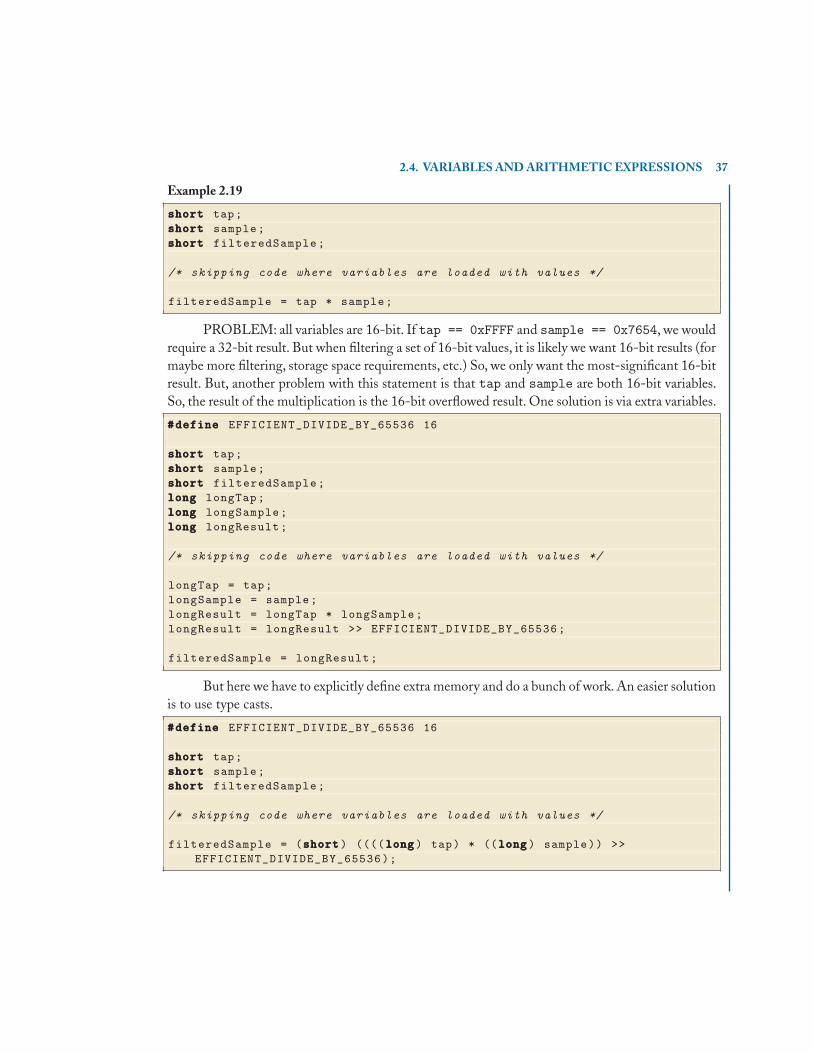
2.4. VARIABLES AND ARITHMETIC EXPRESSIONS 37
Example 2.19
shortshortshort tap;shortshortshort sample;shortshortshort filteredSample;
/* skipping code where variables are loaded with values */
filteredSample = tap * sample;
PROBLEM: all variables are 16-bit. If tap == 0xFFFF and sample == 0x7654, we wouldrequire a 32-bit result. But when filtering a set of 16-bit values, it is likely we want 16-bit results (formaybe more filtering, storage space requirements, etc.) So, we only want the most-significant 16-bitresult. But, another problem with this statement is that tap and sample are both 16-bit variables.So, the result of the multiplication is the 16-bit overflowed result. One solution is via extra variables.
###definedefinedefine EFFICIENT_DIVIDE_BY_65536 16
shortshortshort tap;shortshortshort sample;shortshortshort filteredSample;longlonglong longTap;longlonglong longSample;longlonglong longResult;
/* skipping code where variables are loaded with values */
longTap = tap;longSample = sample;longResult = longTap * longSample;longResult = longResult >> EFFICIENT_DIVIDE_BY_65536;
filteredSample = longResult;
But here we have to explicitly define extra memory and do a bunch of work. An easier solutionis to use type casts.
###definedefinedefine EFFICIENT_DIVIDE_BY_65536 16
shortshortshort tap;shortshortshort sample;shortshortshort filteredSample;
/* skipping code where variables are loaded with values */
filteredSample = (shortshortshort) ((((longlonglong) tap) * ((longlonglong) sample)) >>EFFICIENT_DIVIDE_BY_65536);

38 2. ANSI C
2.4.3 CONSTANTSSeveral methods are available for specifying constant values in the C programming language. Thefirst method is immediate placement of the desired value.
Example 2.20 Decimal constant values include the following statements.
1234 /* is an int */1234l /* is a long */1234L /* is a long */1234u /* is an unsigned int */1234U /* is an unsigned int */1234ul /* is an unsigned long */1234UL /* is an unsigned long */
Note that usually you don’t need to bother with the L’s or U’s, as the compiler manages thisautomatically. A leading 0 on a constant means octal (base-8). A leading 0x on a constant meanshexadecimal (base-16). It is a misconception that a leading 0b on a constant means binary (base-2),but this is not true for ANSI C. However, some compilers do support some variations of binaryconstants.
Example 2.21
Base-10 Base-8 Base-16 Base-1631 037 0x1f 0x1F5349 012345 0x14e5 0x14E5
It is considered good coding practice to define all constants (except 0 and 1, where meaning isobvious) in a header file or at the top of the current source file. This is done by creating a macro withthe preprocessor directive statement #define. Before compilation occurs, the preprocessor replacesall occurrences of the macro label with its defined value. The compiler parses the result, just like the#include directives. Using constant macros is analogous to using meaningful variable labels andfunction names. Doing so leads to self-documenting code and, ideally, the near-elimination of allcomments.
Example 2.22
###definedefinedefine SPECIAL_MAGIC_NUMBER 3
/* skipping many lines */
intintint primeNumber;
/* skipping many lines */
primeNumber = SPECIAL_MAGIC_NUMBER;
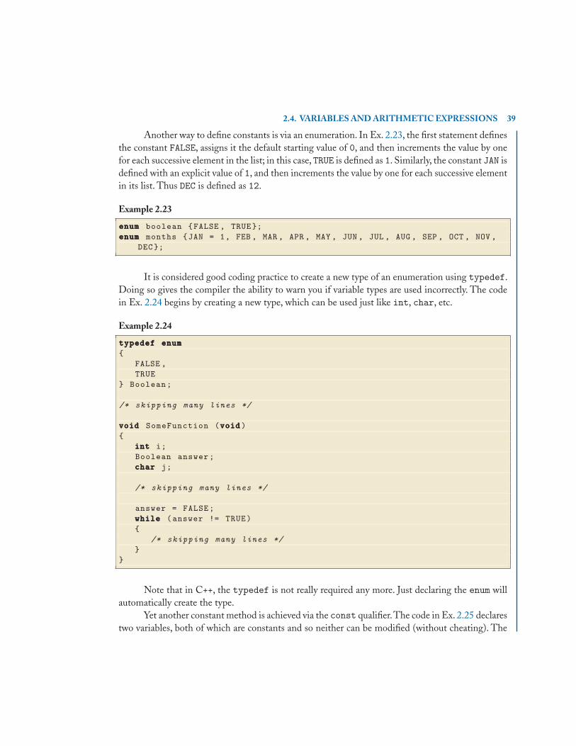
2.4. VARIABLES AND ARITHMETIC EXPRESSIONS 39
Another way to define constants is via an enumeration. In Ex. 2.23, the first statement definesthe constant FALSE, assigns it the default starting value of 0, and then increments the value by onefor each successive element in the list; in this case, TRUE is defined as 1. Similarly, the constant JAN isdefined with an explicit value of 1, and then increments the value by one for each successive elementin its list. Thus DEC is defined as 12.
Example 2.23
enumenumenum boolean {FALSE , TRUE};enumenumenum months {JAN = 1, FEB , MAR , APR , MAY , JUN , JUL , AUG , SEP , OCT , NOV ,
DEC};
It is considered good coding practice to create a new type of an enumeration using typedef.Doing so gives the compiler the ability to warn you if variable types are used incorrectly. The codein Ex. 2.24 begins by creating a new type, which can be used just like int, char, etc.
Example 2.24
typedeftypedeftypedef enumenumenum{
FALSE ,TRUE
} Boolean;
/* skipping many lines */
voidvoidvoid SomeFunction (voidvoidvoid){
intintint i;Boolean answer;charcharchar j;
/* skipping many lines */
answer = FALSE;whilewhilewhile (answer != TRUE){
/* skipping many lines */}
}
Note that in C++, the typedef is not really required any more. Just declaring the enum willautomatically create the type.
Yet another constant method is achieved via the const qualifier.The code in Ex. 2.25 declarestwo variables, both of which are constants and so neither can be modified (without cheating). The
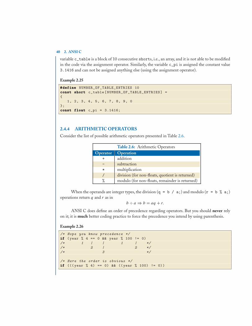
40 2. ANSI C
variable c_table is a block of 10 consecutive shorts, i.e., an array, and it is not able to be modifiedin the code via the assignment operator. Similarly, the variable c_pi is assigned the constant value3.1416 and can not be assigned anything else (using the assignment operator).
Example 2.25
###definedefinedefine NUMBER_OF_TABLE_ENTRIES 10constconstconst shortshortshort c_table[NUMBER_OF_TABLE_ENTRIES] ={
1, 2, 3, 4, 5, 6, 7, 8, 9, 0};constconstconst floatfloatfloat c_pi = 3.1416;
2.4.4 ARITHMETIC OPERATORSConsider the list of possible arithmetic operators presented in Table 2.6.
Table 2.6: Arithmetic OperatorsOperator Operation
+ addition- subtraction* multiplication/ division (for non-floats, quotient is returned)% modulo (for non-floats, remainder is returned)
When the operands are integer types, the division (q = b / a;) and modulo (r = b % a;)operations return q and r as in
b ÷ a ⇒ b = aq + r.
ANSI C does define an order of precedence regarding operators. But you should never relyon it; it is much better coding practice to force the precedence you intend by using parenthesis.
Example 2.26
/* Hope you know precedence */ififif (year % 4 == 0 && year % 100 != 0)/* 1 | | 1 | *//* 2 | 2 *//* 3 */
/* Here the order is obvious */ififif ((( year % 4) == 0) && ((year % 100) != 0))
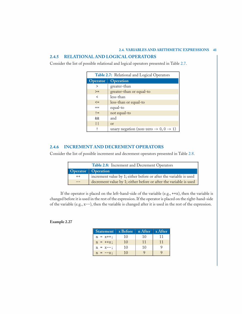
2.4. VARIABLES AND ARITHMETIC EXPRESSIONS 41
2.4.5 RELATIONAL AND LOGICAL OPERATORSConsider the list of possible relational and logical operators presented in Table 2.7.
Table 2.7: Relational and Logical OperatorsOperator Operation
> greater-than>= greater-than or equal-to< less-than<= less-than or equal-to== equal-to!= not equal-to&& and|| or! unary negation (non-zero → 0, 0 → 1)
2.4.6 INCREMENT AND DECREMENT OPERATORSConsider the list of possible increment and decrement operators presented in Table 2.8.
Table 2.8: Increment and Decrement OperatorsOperator Operation
++ increment value by 1; either before or after the variable is used-- decrement value by 1; either before or after the variable is used
If the operator is placed on the left-hand-side of the variable (e.g., ++x), then the variable ischanged before it is used in the rest of the expression. If the operator is placed on the right-hand-sideof the variable (e.g., x--), then the variable is changed after it is used in the rest of the expression.
Example 2.27
Statement x Before n After x Aftern = x++; 10 10 11n = ++x; 10 11 11n = x--; 10 10 9n = --x; 10 9 9

42 2. ANSI C
Table 2.9: Bitwise OperatorsOperator Operation
& AND (boolean intersection)| OR (boolean union)ˆ XOR (boolean exclusive-or)<< left shift>> right shift˜ NOT (boolean negation, i.e., ones’ complement)
2.4.7 BITWISE OPERATORSConsider the list of possible bitwise operators presented in Table 2.9.
Bitwise operations occur on a per-bit level; Fig. 2.5 shows the operation d = c & b, assumingall three variables are declared as unsigned char (assumed to be 8-bit elements).
c4c5c6c7 c0c1c2c3 b4b5b6b7 b0b1b2b3
d4d5d6d7 d0d1d2d3
Figure 2.5: A bitwise logical AND operation on two 8-bit unsigned integer locations. The result theboolean intersection between each bit position is stored in the respective location of the target memorylocation.
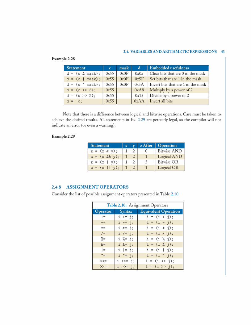
2.4. VARIABLES AND ARITHMETIC EXPRESSIONS 43
Example 2.28
Statement c mask d Embedded usefulnessd = (c & mask); 0x55 0x0F 0x05 Clear bits that are 0 in the maskd = (c | mask); 0x55 0x0F 0x5F Set bits that are 1 in the maskd = (c ˆ mask); 0x55 0x0F 0x5A Invert bits that are 1 in the maskd = (c << 3); 0x55 0xA8 Multiply by a power of 2d = (c >> 2); 0x55 0x15 Divide by a power of 2d = ˜c; 0x55 0xAA Invert all bits
Note that there is a difference between logical and bitwise operations. Care must be taken toachieve the desired results. All statements in Ex. 2.29 are perfectly legal, so the compiler will notindicate an error (or even a warning).
Example 2.29
Statement x y z After Operationz = (x & y); 1 2 0 Bitwise ANDz = (x && y); 1 2 1 Logical ANDz = (x | y); 1 2 3 Bitwise ORz = (x || y); 1 2 1 Logical OR
2.4.8 ASSIGNMENT OPERATORSConsider the list of possible assignment operators presented in Table 2.10.
Table 2.10: Assignment OperatorsOperator Syntax Equivalent Operation
+= i += j; i = (i + j);-= i -= j; i = (i - j);*= i *= j; i = (i * j);/= i /= j; i = (i / j);%= i %= j; i = (i % j);&= i &= j; i = (i & j);|= i |= j; i = (i | j);ˆ= i ˆ= j; i = (i ˆ j);<<= i <<= j; i = (i << j);>>= i >>= j; i = (i >> j);

44 2. ANSI C
2.4.9 CONDITIONAL EXPRESSIONThe conditional expression,
((expr) ? trueV alue : f alseV alue),
is a kind-of operator that evaluates any expression and returns a different result based on if theexpression is true (i.e., non-zero) or false (i.e., 0).
Example 2.30 The following two examples result in identical results.
/* This conditional expression ... */z = (a > b) ? c : d;
/* ...is the same as the following code. */ififif (a > b){
z = c;}elseelseelse{
z = d;}
Direct usage of this operator is not advised due to its cryptic appearance; the only benefit iscompressing source code (not machine code), so it does not help anything (other than job-securityseeking engineers). One good application of this expression is via macro definitions such as inEx. 2.31.
Example 2.31
###definedefinedefine MAX(a,b) ((a > b) ? a : b)
/* z will be assigned the maximum of the two values. */z = MAX(x,y);
2.5 CONTROL FLOWAll structural programming languages (even assembly languages) have constructs that allow for analgorithm to execute different instructions depending on various conditions. In general, an expressionis executed and compared to zero providing a true or false result.These boolean conditions are one ofthe cornerstones of microprocessor execution. They can be combined (sometimes this is automaticand hidden) in order to create any number of complex conditions.
2.5. CONTROL FLOW 45
2.5.1 IF-ELSEConsider Ex 2.32.
Example 2.32
ififif (expression)/* Performed when expression != 0 */statement1
elseelseelse/* Performed when expression == 0 */statement2
Note that statementi may be a block of statements surrounded by { }. In fact, it is consideredgood practice to always use { }, even for single statements. Also note that the else is optional.
2.5.2 ELSE-IFConsider Ex 2.33.
Example 2.33
ififif (expression1)/* Performed when expression1 != 0 */statement1
elseelseelse ififif (expression2)/* Performed when (expression1 == 0) and (expression2 != 0) */statement2
elseelseelse/* Performed when all previous expressions are 0 */statement3
Again, all statementi should be blocks surrounded by { }. There can be as many else ifblocks as desired. They are evaluated in order from top to bottom, implying priority is at the top.
2.5.3 SWITCHConsider Ex 2.34.
Example 2.34
switchswitchswitch (expression){
casecasecase constant -expression1:/* Performed when expression == constant -expression1 */statementsbreakbreakbreak;

46 2. ANSI C
casecasecase constant -expression2:/* Performed when expression == constant -expression2 */statementsbreakbreakbreak;
/* skipping other cases */
defaultdefaultdefault:/* Performed when expression != any constant expression */statementsbreakbreakbreak;
}
The statements following the first constant − expressioni label equal to expression areexecuted. Note that break is used to prevent the fall-through condition. That is, without the breakstatement, the code in the subsequent case will be executed. This is allowed by the compiler, butterrible coding practice. It is much better coding practice to “always” place a break at the end ofeach case. If no cases equal the expression, the statements after the default are executed. If nocases equal the expression and no default is listed, nothing will happen.
2.5.4 LOOPS2.5.4.1 For
Example 2.35
forforfor (expression1; expression2; expression3)statement
2.5.4.2 While
Example 2.36
expression1;whilewhilewhile (expression2){
statementexpression3;
}
The two loop styles presented in Ex. 2.35 and Ex. 2.36 are equivalent. Referring to the twoloops, usually the following are true.
2.5. CONTROL FLOW 47
• expression1 is an initialization assignment (e.g., i = 0).
• expression2 is some ending condition (e.g., i < MAGIC_NUMBER).
• expression3 is an increment (e.g., i += MAGIC_INCREMENT, or i++).
2.5.4.3 Do-WhileThe do-while loop presented in Ex. 2.37 repeats statement as long as expression != 0. A nicefeature of this loop style is that statement is always executed at least once prior to the expression
evaluation.
Example 2.37
dododostatement
whilewhilewhile (expression);
2.5.5 INFINITE LOOPSLoops that repeat execution “forever” are called infinite loops. You might be wondering why such aconstruct exists, as once the algorithm enters an infinite loop it doesn’t exit (until execution is haltedby outside force). However, an infinite loop is a very important and fundamental concept necessaryto many applications. For example, consider running a web-browser on your computer. You wouldn’twant the browser to display some information and then quit after it was done; that would makethe application useless. In fact, you want web-browsers (and most applications) to stay runninguntil you issue a command to quit. Thus, at the very lowest level, the web-browser is sitting in aninfinite loop, repeatedly waiting for user input and responding accordingly. Embedded applicationsare fundamentally the same. Imagine how useless an alarm clock that didn’t sit in an infinite loopwould be.
Example 2.38
forforfor (;;)statement
Example 2.39
whilewhilewhile (1)statement
48 2. ANSI C
Example 2.40
dododostatement
whilewhilewhile (1);
Especially in an embedded platform, often the outer-most layer of the program is an infiniteloop, so that the embedded device will continue to function until some reset condition occurs orpower is removed. For example, the Arduino Integrated Development Environment (IDE) hides themain() function from the engineer. Instead, they present the two functions setup() and loop(),which allow the developer to initialize various conditions, and then loop forever. For example, thetext in Ex.2.41 is an Arduino-based “Hello world” program as viewed through the IDE.
Example 2.41
###definedefinedefine DEBUG_OUTPUT_MESSAGE_MAX_LENGTH 80
voidvoidvoid setup(){
charcharchar message[DEBUG_OUTPUT_MESSAGE_MAX_LENGTH ];
snprintf(message , DEBUG_OUTPUT_MESSAGE_MAX_LENGTH , "Hello , World!\n");
Serial.begin (9600);Serial.write(message);
}
voidvoidvoid loop(){}
The actual C++ source code in Ex.2.42 is generated when the user tries to download theprogram to an embedded target.
Example 2.42
###definedefinedefine DEBUG_OUTPUT_MESSAGE_MAX_LENGTH 80
###includeincludeinclude "WProgram.h"voidvoidvoid setup();voidvoidvoid loop();
voidvoidvoid setup(){
charcharchar message[DEBUG_OUTPUT_MESSAGE_MAX_LENGTH ];

2.5. CONTROL FLOW 49
snprintf(message , DEBUG_OUTPUT_MESSAGE_MAX_LENGTH , "Hello , World!\n");
Serial.begin (9600);Serial.write(message);
}
voidvoidvoid loop(){}
intintint main(voidvoidvoid){
init();
setup();
forforfor (;;)loop();
returnreturnreturn 0;}
Notice the general structure inside the main() function begins by initializing various periph-erals, memory, etc., before entering an infinite loop.
2.5.6 MISCELLANEOUS (PLEASE DON’T USE)The following are a part of ANSI C but should “never” be used for the sake of maintainable code.
2.5.6.1 BreakA break allows for the early exit from a loop. It is useful (and actually required for maintainablecode) within a switch statement so the code in subsequent cases is not executed.
Example 2.43 After the loop executes in this example, i == 5 and x == 4.
forforfor (i = 0; i < 10; i++){
ififif (i >= 5){
/* This will cause the loop to quit when i == 5. */breakbreakbreak;
}x = i;
}
50 2. ANSI C
2.5.6.2 ContinueA continue is similar to break in that when executed the remaining code in the loop block isskipped. However, it differs from break in that the loop continues to execute.
Example 2.44 After the loop executes in this example, i == 10 and x == 4.
forforfor (i = 0; i < 10; i++){
ififif (i >= 5){
/* This will cause a jump to the loop start when i >= 5. */continuecontinuecontinue;
}x = i;
}
2.5.6.3 Goto and LabelsWorst of all, goto and labels should be avoided at all costs (and can be). However, one place that isriddled with goto usage is within Linux device drivers, where a number of conditions can cause anerror to occur resulting in the necessary clean-up of any previous allocations.The reality is that gotosin these situations could have been avoided, but it is already very established and somewhat commonpractice. As a result, it is actually better to remain consistent, in spite of the horrible inclusion ofgotos.
Example 2.45
intintint DeviceDriverProbe(voidvoidvoid){/* allocate resource 1 */
ififif ( /* a bad condition occurs */ ){
/* This will cause a direct jump to the label below */gotogotogoto errorHandlerResource1;
}
/* allocate resource 2 */ififif ( /* a bad condition occurs */ ){
/* This will cause a direct jump to the label below */gotogotogoto errorHandlerResource2;
}
/* many more allocations and other things */
returnreturnreturn (0);

2.6. FUNCTIONS AND PROGRAM STRUCTURES 51
errorHandlerResource2:/* some code to clean up resource 2 */
errorHandlerResource1:/* some code to clean up resource 1 */
returnreturnreturn (-1);}
2.6 FUNCTIONS AND PROGRAM STRUCTURESFunctions are isolated blocks of statements that are executed when the function label is called fromelsewhere in the program. When the block of code defining the function finishes, program executionreturns back to the point from which it was called. Function constructs are familiar in many differentlanguages under a variety of names including routines and procedures.
Good coding practice uses functions to modularize source code, assuming the 7 ± 2 rule isfollowed. In other words, functions should not be too big nor too small. Of course, there are alwaysexceptions to the rule. Each function definition has the form presented in Ex. 2.46.
Example 2.46
return_type functionName (argument declarations){
declarations
statements}
Note that various parts are optional and may be absent.
Example 2.47 A minimal (and useless) function.
smallFunction () {}
The function in Ex. 2.47 does nothing and returns nothing. However, it does absorb programspace and CPU cycles if called (unless the compiler is “smart” enough to optimize it out).
If the return_type is omitted, int is assumed. For any non-void return_type, the finalexiting statement from a function is given in Ex. 2.48.

52 2. ANSI C
Example 2.48
returnreturnreturn expression;
Use function prototypes to declare to the compiler the exact return_type and argument decla-rations. Note that this is not required, the compiler can resolve everything without them. However,especially for complex projects with many source files, it is good practice to always specify functionsvia prototypes, such as in Ex. 2.49.
Example 2.49
/* Prototype */return_type functionName (argument declarations);
/* skip lots of code */
/* actual function */return_type functionName (argument declarations){
/* skip code */}
2.7 SCOPE RULESThe scope of a label is the part of the program within which it can be used. Variables may be usedonly in the block in which they are declared. This includes any sub-blocks also declared within theblock. Any block may contain variable declarations. Variables are not visible to any code outside ofthe defining block. Global variables are available to all blocks of code.
Use of the extern keyword makes labels in one source file available to another source file.
Example 2.50 Let fileA.c contain the following code
externexternextern intintint x;externexternextern voidvoidvoid functionName (voidvoidvoid);
voidvoidvoid main (voidvoidvoid){
x = 0;functionName ();
}
Let fileB.c contain the following code
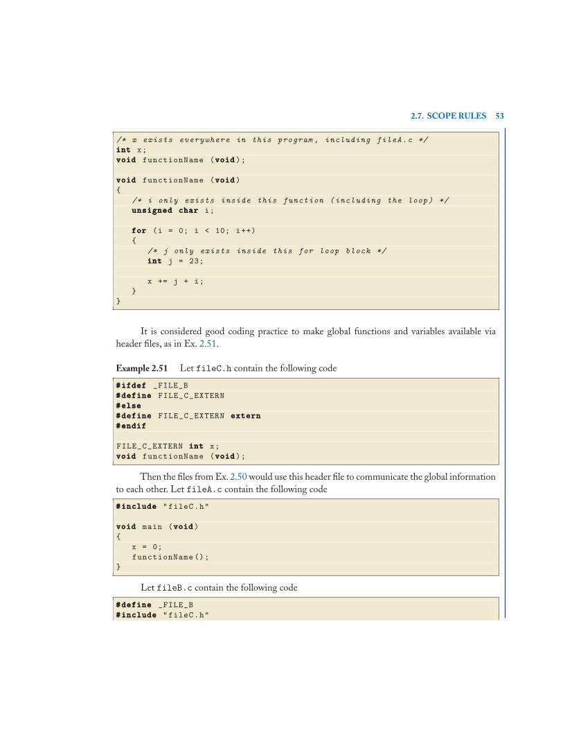
2.7. SCOPE RULES 53
/* x exists everywhere in this program , including fileA.c */intintint x;voidvoidvoid functionName (voidvoidvoid);
voidvoidvoid functionName (voidvoidvoid){
/* i only exists inside this function (including the loop) */unsignedunsignedunsigned charcharchar i;
forforfor (i = 0; i < 10; i++){
/* j only exists inside this for loop block */intintint j = 23;
x += j + i;}
}
It is considered good coding practice to make global functions and variables available viaheader files, as in Ex. 2.51.
Example 2.51 Let fileC.h contain the following code
###ifdefifdefifdef _FILE_B###definedefinedefine FILE_C_EXTERN###elseelseelse###definedefinedefine FILE_C_EXTERN externexternextern###endifendifendif
FILE_C_EXTERN intintint x;voidvoidvoid functionName (voidvoidvoid);
Then the files from Ex. 2.50 would use this header file to communicate the global informationto each other. Let fileA.c contain the following code
###includeincludeinclude "fileC.h"
voidvoidvoid main (voidvoidvoid){
x = 0;functionName ();
}
Let fileB.c contain the following code
###definedefinedefine _FILE_B###includeincludeinclude "fileC.h"

54 2. ANSI C
voidvoidvoid functionName (voidvoidvoid){
unsignedunsignedunsigned charcharchar i;
forforfor (i = 0; i < 10; i++){
intintint j = 23;
x += j + i;}
}
By placing the #define _FILE_B in fileB.c before the header file is included, it causes thepreprocessor to define a blank macro. This causes the compiler to allocate the necessary memory forvariable x. fileA.c simply includes the header file without defining anything, and so x is declaredas an external variable within that file.
The keyword static limits the scope of a global variable to just within the file declaring it.
Example 2.52 Here, y is still a global variable, but the compiler will not allow any other files inthe build process to have access to it because of the static keyword.
###definedefinedefine _FILE_B###includeincludeinclude "fileC.h"
/* y is global only within this file */staticstaticstatic intintint y;
voidvoidvoid functionName (voidvoidvoid){}
Additionally, when static is used inside a local block, it makes a variable persistent. However,the variable is still only accessible within that block.
Example 2.53 The first call to the test() function initializes i == 0. On the next call, i is notre-initialized to zero; instead, it contains the value it had when the function exited previously (i.e.,i == 1).
voidvoidvoid test (voidvoidvoid){
staticstaticstatic intintint i = 0;i += 1;
}
2.7. SCOPE RULES 55
Note that there are compiler rules regarding scope when two variables are named the samething in nested blocks.
Example 2.54 Here there are two versions of the variable i.They do not refer to the same memorylocations – they are different variables with the same name.
intintint i;
voidvoidvoid functionName (voidvoidvoid){
unsignedunsignedunsigned charcharchar i;
/* which i is valid in here? */}
To avoid the confusing problem posed in Ex. 2.54, a consistent coding convention is usefulfor the sake of maintainable code. An example coding convention might include the rules presentedin Table 2.11. A set of coding convention rules from an embedded software company is presentedin Apx. D.
Table 2.11: Example Cod-ing Convention RulesName type Conventionconstant CONSTANTglobal g_namestatic global m_namelocal name
Example 2.55 Consider Ex. 2.54 rewritten using the convention presented in Table 2.11.
intintint g_i;
voidvoidvoid functionName (voidvoidvoid){
unsignedunsignedunsigned charcharchar i;
/* no question about i now */}
The keyword register advises the compiler that the variable will be accessed a lot and shouldbe placed in a machine register. In ANSI C, the compiler is free to ignore this directive (and oftendoes).
56 2. ANSI C
Example 2.56
registerregisterregister intintint x;
Some compilers provide the keyword volatile, which advises the compiler that the variablemay be changed externally, i.e., from outside the CPU, such that the processor can’t assume a cachedvalue. Because most programs are completely deterministic, the compiler can analyze the sourcecode and determine situations where it can optimize out instructions and still achieve the intendedbehavior. Part of this optimization process assumes that values stored in memory locations can onlychange if the CPU writes to them. Thus, the compiler can remove statements if values haven’t beenwritten to explicitly. However, there are many situations in embedded applications when the programneeds to access memory-mapped hardware that may have its value change due to external stimuli.If the compiler is not informed about this behavior, it can unintentionally optimize out certaininstructions. The result is that real-time hardware values may not be updated by the program, eventhough C instructions were written to do so. By using the volatile keyword on a variable, thecompiler is told not assume the memory location hasn’t changed. Note that the volatile keywordis not part of the ANSI C standard.
Example 2.57
volatilevolatilevolatile intintint x;
As a result of the volatile keyword, the compiler is unable to optimize out certain statementsdue to memory caching. Thus, sometimes it is helpful to use the keyword on a regular variable totrick the compiler into preserving some statements that you don’t want removed.
2.8 POINTERS AND ARRAYS
A pointer is a variable that contains an address, usually of another variable, but it can be anything inthe addressable space. Memory, in general, is just a block of addressable bits that may be manipulatedin various-sized groups,but the bits are all physically the same.Generally, the sizes listed inTable 2.12represent the contiguous memory locations, usually along address boundaries.
Table 2.12: Typical Contiguous Memory SizesType Number of 8-bit Units Total Contiguous Bitschar 1 8short 2 16long 4 32

2.8. POINTERS AND ARRAYS 57
Then, a pointer is a group of cells (usually 2 or 4 8-bit cells) that holds an address.
Example 2.58 Suppose the following variables are allocated in the specified order. Let r be apointer that points to l, q be a pointer that points to s, and p be a pointer that points to c. Also,let s be a 16-bit short, l be a 32-bit long, and c be an 8-bit char. Note that in this hypotheticalexample, pointers are 32-bit variables meaning the processor has 32-bit addressable space.
... ......
r q p s l c
Figure 2.6: A schematic view of memory. The smallest division represents one 8-bit memory location.The height of the division line represents the byte-, short-, and long-address boundaries.
As indicated by Ex. 2.58, the amount of space reserved for any pointer is the same, no matterto what type the pointer is pointing. In the example, 32-bits are assumed for the addressable space;this is based on the architecture of the CPU. One way to make the pointer point to some variable isvia the unary operator &, which gives the address of the label on its right-hand-side.
Example 2.59
p = &c;q = &s;r = &l;
Note that &p is the address of the pointer variable.
One way to access the contents of a variable using a pointer is via the unary operator *, whichis called the dereferencing operator.
Example 2.60 At the end of these three statements, variable c is loaded with the value 10 via thedereference of its address in pointer p.
p = &c;c = 0;*p = 10;
/* now it is true that (c == 10) */

58 2. ANSI C
To declare a pointer, just add the * symbol to the left of the variable name.
Example 2.61
charcharchar *p;shortshortshort *q;longlonglong *r;
This syntax is intended as a mnemonic.Using Ex.2.61, the notation implies that the expression*p is a char, *q is a short and *r is a long. Note that as seen before, the space allocated to holdp, q and r is all the same (usually 32-bits on modern microprocessors), but what they point to isdifferent. This matters to the compiler when pointer indexing is used.
You can create pointers to any type, for example:
• pointers to other pointers;
• pointers to functions;
• pointers to any type of array; and
• pointers to structure types.
The unary operators * and & have a very high precedence. However, the unary operators ++and -- have the same level of operator precedence. When the compiler parses a line of source code,it resolves operators with the same precedence from right-to-left. Thus, the statement *p++; willhave a very different result compared to (*p)++;.The former case will increment the address storedin p first, then dereference the result. The latter case will read the dereferenced address first andincrement the resulting value without changing the address stored in p. Several examples of usingpointer indexing are listed in Table 2.13, assuming that char c = 5;, char *p;, and p = &c;.Notice that all but the final statement are equivalent.
Table 2.13: Pointer Indexing OperationsBefore After
Instruction &c = 100 101 p &c = 100 101 p *pc = *p + 1; 5 0 100 6 0 100 6*p += 1; 5 0 100 6 0 100 6++*p; 5 0 100 6 0 100 6(*p)++; 5 0 100 6 0 100 6*p++; 5 0 100 5 0 101 0
Arrays are blocks of consecutive types. An array variable is similar to a pointer of that typethat has been initialized to the address of the first entry of the block. That is, pointers are similar
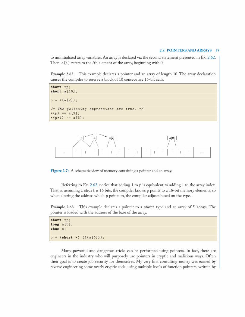
2.8. POINTERS AND ARRAYS 59
to uninitialized array variables. An array is declared via the second statement presented in Ex. 2.62.Then, a[i] refers to the ith element of the array, beginning with 0.
Example 2.62 This example declares a pointer and an array of length 10. The array declarationcauses the compiler to reserve a block of 10 consecutive 16-bit cells.
shortshortshort *p;shortshortshort a[10];
p = &(a[2]);
/* The following expressions are true. */*(p) == a[2];*(p+1) == a[3];
......
p a a[2] a[9]
Figure 2.7: A schematic view of memory containing a pointer and an array.
Referring to Ex. 2.62, notice that adding 1 to p is equivalent to adding 1 to the array index.That is, assuming a short is 16 bits, the compiler knows p points to a 16-bit memory elements, sowhen altering the address which p points to, the compiler adjusts based on the type.
Example 2.63 This example declares a pointer to a short type and an array of 5 longs. Thepointer is loaded with the address of the base of the array.
shortshortshort *p;longlonglong a[5];charcharchar c;
p = (shortshortshort *) (&(a[0]));
Many powerful and dangerous tricks can be performed using pointers. In fact, there areengineers in the industry who will purposely use pointers in cryptic and malicious ways. Oftentheir goal is to create job security for themselves. My very first consulting money was earned byreverse engineering some overly cryptic code, using multiple levels of function pointers, written by
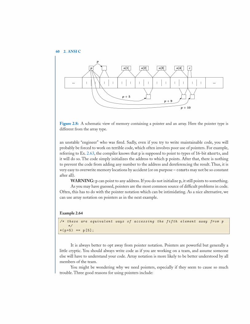
60 2. ANSI C
......
p a[1] a[2] a[3] a[4]
p
c
p + 5
p + 9
p + 10
Figure 2.8: A schematic view of memory containing a pointer and an array. Here the pointer type isdifferent from the array type.
an unstable “engineer” who was fired. Sadly, even if you try to write maintainable code, you willprobably be forced to work on terrible code, which often involves poor use of pointers. For example,referring to Ex. 2.63, the compiler knows that p is supposed to point to types of 16-bit shorts, andit will do so. The code simply initializes the address to which p points. After that, there is nothingto prevent the code from adding any number to the address and dereferencing the result. Thus, it isvery easy to overwrite memory locations by accident (or on purpose – consts may not be so constantafter all).
WARNING: p can point to any address. If you do not initialize p, it still points to something.As you may have guessed, pointers are the most common source of difficult problems in code.
Often, this has to do with the pointer notation which can be intimidating. As a nice alternative, wecan use array notation on pointers as in the next example.
Example 2.64
/* these are equivalent ways of accessing the fifth element away from p*/
*(p+5) == p[5];
It is always better to opt away from pointer notation. Pointers are powerful but generally alittle cryptic. You should always write code as if you are working on a team, and assume someoneelse will have to understand your code. Array notation is more likely to be better understood by allmembers of the team.
You might be wondering why we need pointers, especially if they seem to cause so muchtrouble. Three good reasons for using pointers include:
2.8. POINTERS AND ARRAYS 61
1. Passing information in and out of function calls.
2. Dynamic memory allocation.
3. Especially in embedded devices, we can use pointers to access memory-mapped registers inorder to manage various peripheral devices. We will be using pointers for this extensively lateron.
2.8.1 PASSING BY REFERENCEConsider the following code which does not function as intended.
Example 2.65
voidvoidvoid main (voidvoidvoid){
shortshortshort a = 10;shortshortshort b = 13;
swap (a,b);
/* a == ?, b == ? */}
voidvoidvoid swap (shortshortshort x, shortshortshort y){
shortshortshort temp;
temp = x;x = y;y = temp;
}
The code in Ex. 2.65 will not do what we want because the values loaded into a and b arepassed into the function; that is, the values are copied onto the stack or into a register so the functioncan access them. Fig. 2.9 shows how the stack pointer (SP) is used to temporarily store the returnaddress so the program counter knows where to return to, and then the local variables x (whichholds a copy of the a value), y (which holds a copy of the b value) and temp. The values belowthe “memory” represent how the values in the local memory change after each instruction of thefunction is executed. At the very end of the function, the stack pointer “pops” all the memory bymoving back from where it started, so the changed memory is lost forever. Notice the original valuesare still safely stored in a and b.
To correct the problem from Ex. 2.65, consider using pointers.

62 2. ANSI C
......
SP
x
return address 10
a b
13
y temp
10 13
10
13
10
...
Figure 2.9: The memory contents while the code in Ex. 2.65 is executed.
Example 2.66
voidvoidvoid main (voidvoidvoid){
shortshortshort a = 10;shortshortshort b = 13;
/* Now we pass the address of the variables we want to change. */swap (&a,&b);
/* a == ?, b == ? */}
voidvoidvoid swap (shortshortshort *x, shortshortshort *y){
shortshortshort temp;
temp = *x;*x = *y;*y = temp;
}
Now, the code in Ex. 2.66 does what we intended because the addresses of a and b are passedinto the function. The function accesses their values by indirect reference via the pointers x and y.The memory contents change as indicated in Fig. 2.10.
Another reason to use pointers is for passing large pieces of memory into a function. Forexample, suppose we wanted to pass an array of 10,000 longs into a function. If you tried passingby value, the stack would need to hold all 80,000 bytes. However, if we used a pointer to the base ofthe array, the stack only needs to hold the 4-byte base address.
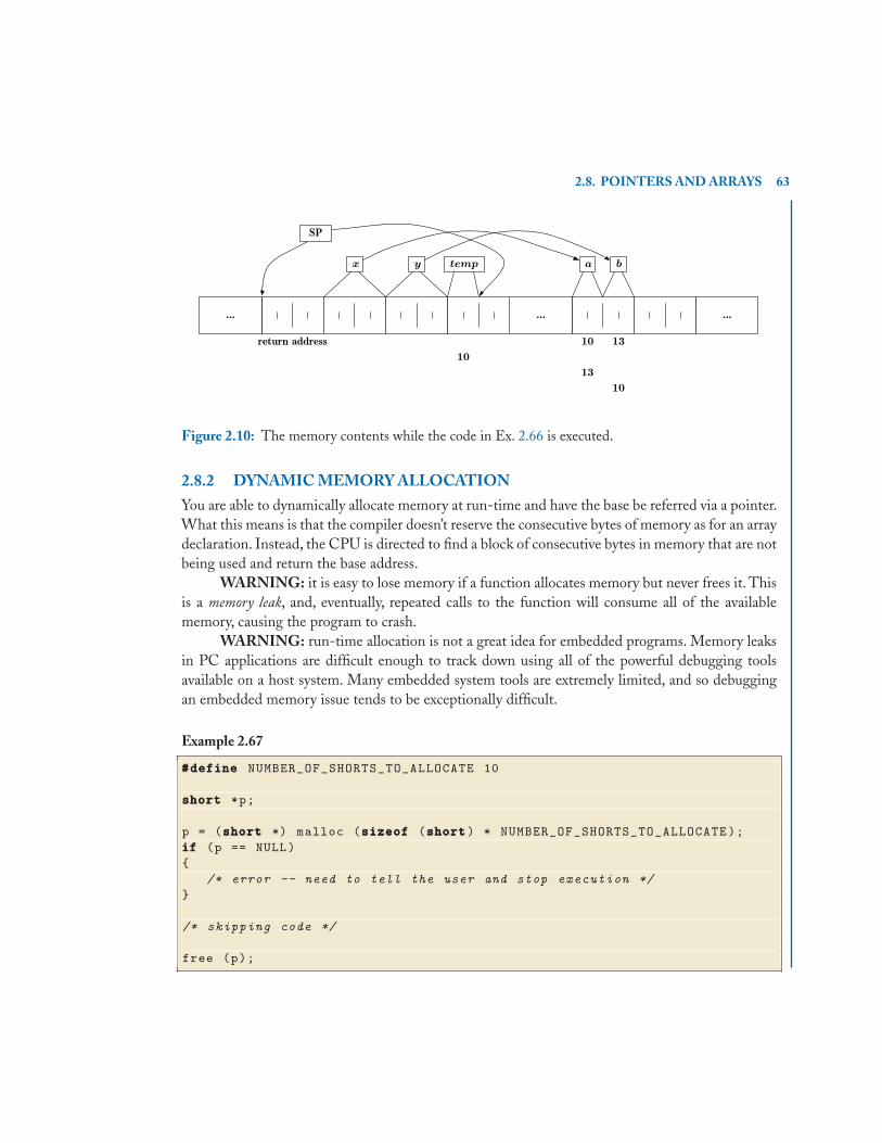
2.8. POINTERS AND ARRAYS 63
......
SP
x
return address 10
a b
13
y temp
10
13
10
...
Figure 2.10: The memory contents while the code in Ex. 2.66 is executed.
2.8.2 DYNAMIC MEMORY ALLOCATIONYou are able to dynamically allocate memory at run-time and have the base be referred via a pointer.What this means is that the compiler doesn’t reserve the consecutive bytes of memory as for an arraydeclaration. Instead, the CPU is directed to find a block of consecutive bytes in memory that are notbeing used and return the base address.
WARNING: it is easy to lose memory if a function allocates memory but never frees it. Thisis a memory leak, and, eventually, repeated calls to the function will consume all of the availablememory, causing the program to crash.
WARNING: run-time allocation is not a great idea for embedded programs. Memory leaksin PC applications are difficult enough to track down using all of the powerful debugging toolsavailable on a host system. Many embedded system tools are extremely limited, and so debuggingan embedded memory issue tends to be exceptionally difficult.
Example 2.67
###definedefinedefine NUMBER_OF_SHORTS_TO_ALLOCATE 10
shortshortshort *p;
p = (shortshortshort *) malloc (sizeofsizeofsizeof (shortshortshort) * NUMBER_OF_SHORTS_TO_ALLOCATE);ififif (p == NULL){
/* error -- need to tell the user and stop execution */}
/* skipping code */
free (p);

64 2. ANSI C
The C operator macro sizeof() returns the number of bytes used by the given argument.The function malloc() returns the base to a block of requested bytes. Referring to the code inEx. 2.67, the processor must locate 10 consecutive unused short cells and return the base address. Ifthey cannot be found, the special “invalid address” NULL is returned. Once the code is finished usingthe allocated memory, it needs to be returned to the state of unused memory via a call to free().
Example 2.68 An alternative form for dynamic memory allocation.
###definedefinedefine NUMBER_OF_SHORTS_TO_ALLOCATE 10
shortshortshort *p;
p = (shortshortshort *) calloc (NUMBER_OF_SHORTS_TO_ALLOCATE , sizeofsizeofsizeof (shortshortshort));ififif (p == NULL){
/* error -- need to tell the user and stop execution */}
/* skipping code */
free (p);
Example 2.69 Code can adjust the size of the allocated memory with the following.
###definedefinedefine NUMBER_OF_SHORTS_TO_ALLOCATE 10###definedefinedefine NUMBER_OF_SHORTS_TO_REALLOCATE 12
shortshortshort *p;
p = (shortshortshort *) calloc (NUMBER_OF_SHORTS_TO_ALLOCATE , sizeofsizeofsizeof (shortshortshort));ififif (p == NULL){
/* error -- need to tell the user and stop execution */}
/* skipping code */
p = (shortshortshort *) realloc (p, sizeofsizeofsizeof (shortshortshort) *NUMBER_OF_SHORTS_TO_REALLOCATE);
ififif (p == NULL){
/* error -- need to tell the user and stop execution */}
free (p);
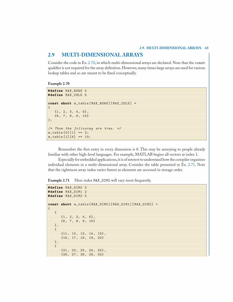
2.9. MULTI-DIMENSIONAL ARRAYS 65
2.9 MULTI-DIMENSIONAL ARRAYSConsider the code in Ex. 2.70, in which multi-dimensional arrays are declared. Note that the constqualifier is not required for the array definition. However, many times large arrays are used for variouslookup tables and so are meant to be fixed conceptually.
Example 2.70
###definedefinedefine MAX_ROWS 2###definedefinedefine MAX_COLS 5
constconstconst shortshortshort m_table[MAX_ROWS ][ MAX_COLS] ={
{1, 2, 3, 4, 5},{6, 7, 8, 9, 10}
};
/* Then the following are true. */m_table [0][1] == 2;m_table [1][4] == 10;
Remember the first entry in every dimension is 0. This may be annoying to people alreadyfamiliar with other high-level languages. For example, MATLAB begins all vectors at index 1.
Especially for embedded applications, it is of interest to understand how the compiler organizesindividual elements in a multi-dimensional array. Consider the table presented in Ex. 2.71. Notethat the rightmost array index varies fastest as elements are accessed in storage order.
Example 2.71 Here index MAX_DIM2 will vary most frequently.
###definedefinedefine MAX_DIM0 3###definedefinedefine MAX_DIM1 2###definedefinedefine MAX_DIM2 5
constconstconst shortshortshort m_table[MAX_DIM0 ][ MAX_DIM1 ][ MAX_DIM2] ={
{{1, 2, 3, 4, 5},{6, 7, 8, 9, 10}
},{
{11, 12, 13, 14, 15},{16, 17, 18, 19, 20}
},{
{21, 22, 23, 24, 25},{26, 27, 28, 29, 30}

66 2. ANSI C
},};
/* Then the following are true. */m_table [0][1][2] == 8;m_table [2][1][3] == 29;
...12111098765431 2...
m_table
[0][0][0] [0][1][0] [1][0][1]
Figure 2.11: The memory contents for the multi-dimensional array of the code listing.
Regarding pointers, [] have higher precedence than unary *.
Example 2.72 The following chart lists some of the different declarations possible using array andpointer notations.
Primary Each Primary Total AllocationDeclaration Number Element Type at Compile Timeshort a[10][20]; 10 Array of 20 shorts 10 × 20 = 200 shorts.short *b[10]; 10 Pointer to 1 short 10 pointers to shorts.
All 10 pointers are uninitialized.short (*c)[20]; 1 Pointer to array of 1 uninitialized pointer.
20 shorts
Now suppose we had the following code.
typedeftypedeftypedef shortshortshort (* PointerToArrayType) [20];
shortshortshort i;
forforfor (i = 0; i < 10; i++){
b[i] = (shortshortshort *) malloc (sizeofsizeofsizeof (shortshortshort) * 20);}c = (PointerToArrayType) malloc (sizeofsizeofsizeof (shortshortshort) * 20 * 10);

2.10. FUNCTION POINTERS 67
In a sense, a, b and c are all equivalent, as in the following code.
shortshortshort i;shortshortshort j;
forforfor (i = 0; i < 10; i++){
forforfor (j = 0; j < 20; j++){
a[i][j] = SOME_MAGIC_NUMBER;(b[i])[j] = SOME_MAGIC_NUMBER;c[i][j] = SOME_MAGIC_NUMBER;
}}
So, in all cases, we are able to read/write 200 short values. Also, we are able to use arraynotation in all cases. What’s the difference?
a b cCompile-Time 200 consecutive 10 consecutive 1 short (*)[20]
Memory short short *
Run-Time 10 non-consecutive 200 consecutiveMemory blocks of 20 short
consecutive shortComments Always available; Most memory usage; Pointer required;
no memory management; fragmented memory; memory management;fixed array size. variable array size. fixed array size.
Bytes Required 200 × sizeof(short) (10 × sizeof(short *))+ (1 × sizeof(short *))+(10 × 20 × sizeof(short)) (200 × sizeof(short))
Based on the differences, c is nearly the same as a with the exception that it requires a pointer anddynamic memory allocation. As a result, typically either method a or b is used.
2.10 FUNCTION POINTERSWhile a function is not a variable, it is a label and still has an address. As a result, it is possibleto define function pointers, which can be assigned and treated as any other pointer variable. Forexample, they can be passed into other functions, in particular, callbacks into Real-Time OperatingSystems (RTOSes) or hooks in an Interrupt Service Routine (ISR) vector table. We will see moreinformation about ISRs on the Arduino in Ch. 9. It turns out that the Wiring Arduino softwarelibrary uses an array of function pointers in order to allow casual users the ability to dynamically setarbitrary functions as ISRs. This material is beyond the scope of this book.
Notation to declare a function pointer is

68 2. ANSI C
return_type (* variableName)(argument_list);
Example 2.73
intintint (* comp) (voidvoidvoid *, voidvoidvoid *);charcharchar * (* weird) (voidvoidvoid);
Variable comp is a pointer to a function that returns an int and takes two generic pointersas arguments. Variable weird is a pointer to a function that returns a char pointer and takes noarguments.
Note that the best way to use function pointers is by defining a new type as in Ex. 2.74 thatshows a method for implementing a state machine in software.
Example 2.74
typedeftypedeftypedef voidvoidvoid (* PointerToStateFunction) (intintint);
typedeftypedeftypedef enumenumenum{
STATE_ONE ,STATE_TWO
} States;
typedeftypedeftypedef structstructstruct{
States theState;PointerToStateFunction theStateFunction;
} StateEntry;
voidvoidvoid StateOne (intintint Message);voidvoidvoid StateTwo (intintint Message);
staticstaticstatic States m_state;constconstconst staticstaticstatic StateEntry m_stateTable [] ={
{STATE_ONE , StateOne},{STATE_TWO , StateTwo},
};
m_state = STATE_ONE;
voidvoidvoid ProcessMessages (voidvoidvoid){
intintint message;

2.11. STRUCTURES 69
/* wait until some asynchronous event happens and set message */
m_stateTable[m_state ]. theStateFunction(message);}
Notice at the very end of the code listing in Ex. 2.74, the variable m_stateTable (which isa structure type, see Sec. 2.11) is used to call a function (either StateOne() or StateTwo()).
Function pointers are very tricky,but often used in embedded programming for various reasonsincluding:
• callbacks into RTOSes;
• ISR handling;
• I/O port interfacing to higher level;
• as shown in Ex. 2.74 to reduce code size at expense of a complexity.
Be aware of operator precedence as in the next example.
Example 2.75
/* function returning pointer to int */intintint *f (voidvoidvoid);
/* pointer to function returning int */intintint (*f) (voidvoidvoid);
2.11 STRUCTURESA structure is a collection of one or more variables, possibly of different types, grouped together undera single name for convenient handling. Similar constructs are available in most high-level languagessuch as records in Pascal and classes in C++.
Notation for defining a structure type is as presented in Ex. 2.76.
Example 2.76
structstructstruct TagPoint{
intintint x;intintint y;
};
70 2. ANSI C
Referring to Ex. 2.76, struct is a keyword introducing the structure declaration, which is thelist in braces { }. TagPoint is an optional structure tag. It names this kind of structure and maybe used as shorthand for the part of the declaration in braces. The labels x and y are called membersof the structure. They are “within the scope” of this structure.
To see how we can declare structure variables, consider the code listing in Ex. 2.77.
Example 2.77 The following
structstructstruct TagPoint x, y, z;
is analogous to
intintint x, y, z;
Both cases declare x, y and z as variables of the same type.
Note that a structure declaration followed by no variables does not allocate any space; it justdefines the template for later use.
Example 2.78
structstructstruct TagPoint point;structstructstruct TagPoint maxPoint = {320, 200};
The code presented in Ex. 2.78 will use and allocate the space for the structure definitionpreviously stated. The second variable maxPoint will declare a variable and initialize all members.
The . operator connects the structure variable name and the member name. So, for theproceeding example, the following are true.
Example 2.79
maxPoint.x == 320;maxPoint.y == 200;
Now consider building structures using other types such as other structures.
Example 2.80
structstructstruct TagRectangle{
structstructstruct TagPoint upperLeftCorner;structstructstruct TagPoint lowerRightCorner;
};
structstructstruct TagRectangle polygon;
polygon.upperLeftCorner.x = 320;

2.11. STRUCTURES 71
Legal operations on structures include assignment, copy, passing type into functions, returningtype from functions,get address via &, and access members.Notice the list does not include operationslike comparison, increment, decrement, etc.
Example 2.81
structstructstruct TagPoint add (structstructstruct TagPoint p1, structstructstruct TagPoint p2){
structstructstruct TagPoint temp;
temp = p1;
temp.x += p2.x;temp.y += p2.y;
returnreturnreturn (temp);}
The code in Ex. 2.81 works fine, but consider all of the memory getting copied to/from thestack; especially in cases when the structure has several members. A more efficient alternative is topass the address of the structure variables, and then use pointers within the function. Pointers tostructures are just like any other pointer variables. However, pointers to structures are so commonthat a special operator -> is used to dereference the member of a structure via a pointer.
Example 2.82
structstructstruct TagPoint *pp;structstructstruct TagPoint p3;
pp = &p3;
/* The following are equivalent. */(*pp).x == pp->x;
Be careful of operator precedence.
Example 2.83
(*pp).x == pp->x;(*pp).x != *(pp.x);*pp.x == *(pp.x);
That is, since . has higher precedence than *, we would need (). The better choice is to use->. Note that both . and -> associate from left-to-right.
72 2. ANSI C
Example 2.84
structstructstruct TagRectangle r;structstructstruct TagRectangle *rp;
rp = &r;r.upperLeftCorner.x = 5;
/* The following are all equivalent. */rp->upperLeftCorner.x == 5;(r.upperLeftCorner).x == 5;(rp->upperLeftCorner).x == 5;
Arrays of structures are just as before using the type of structure. Note that you shouldn’tassume the size of a structure is the sum of the sizes of members. Address boundary alignmentrequirements will force “holes” in a structure. Consider the following example.
Example 2.85 Compare the memory of the following two variables.
structstructstruct{
charcharchar c;longlonglong l;
} x;
structstructstruct{
longlonglong l;charcharchar c;
} y;
Here x requires 8 bytes, while y only uses 5 bytes, as indicated in Fig. 2.12.
Referring to Ex. 2.85, the memory holes occur as a result of the byte-boundaries necessaryin computer architecture addressing where masking-off the least significant address bits is usedto address larger units. The sizeof() operator returns the proper value, so sizeof(x)== 8 andsizeof(y)== 5. Note that these amounts are assuming the compiler does not perform any kind ofoptimization. However, even with optimizations, there are still situations where structure memorywill contain unused bytes.
Recursion using pointers is allowed, as indicated in the code listing of Ex. 2.86.
Example 2.86
structstructstruct TagOfNode{
charcharchar *word;

2.11. STRUCTURES 73
intintint count;structstructstruct TagOfNode *left;structstructstruct TagOfNode *right;
};
...
y
...
x
.c .l .l .c
Figure 2.12: The memory contents for the two structure variables of the code listing.
The last two members of the proceeding code listing are allowed as pointers, but structTagOfNode xwould not be allowed (yet another important reason for pointers).To understand why,imagine that the compiler needs to reserve space for each member. Because of the recursion, thereis no way for the compiler to save the correct amount of structure space for a structure that is stillbeing parsed. However, because all pointers are the same size regardless of the type to which theypoint, the compiler can reserve the proper amount of space without knowing how big the structureis going to be.
2.11.1 TYPEDEFThe keyword typedef creates a new data type name. It is really useful regarding struct types, asindicated in the following example.
Example 2.87
typedeftypedeftypedef structstructstruct TagPoint{
intintint x;intintint y;
} Point;
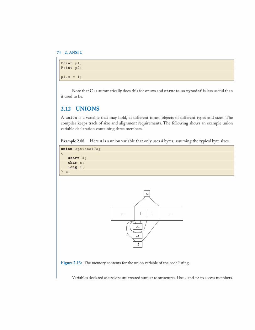
74 2. ANSI C
Point p1;Point p2;
p1.x = 1;
Note that C++ automatically does this for enums and structs, so typedef is less useful thanit used to be.
2.12 UNIONSA union is a variable that may hold, at different times, objects of different types and sizes. Thecompiler keeps track of size and alignment requirements. The following shows an example unionvariable declaration containing three members.
Example 2.88 Here u is a union variable that only uses 4 bytes, assuming the typical byte sizes.
unionunionunion optionalTag{
shortshortshort s;charcharchar c;longlonglong l;
} u;
... ...
u
.s
.l
.c
Figure 2.13: The memory contents for the union variable of the code listing.
Variables declared as unions are treated similar to structures. Use . and -> to access members.
2.13. BIT-FIELDS 75
2.13 BIT-FIELDSEspecially in embedded applications, memory resources are valuable and often scarce. Yet productrequirements can often call for extensive features. As a result, we often need to pay attention to howinformation is being stored in memory. One interesting aspect of C that does not receive a lot ofattention is the ability to pack bits when storage is at a premium. One method for packing bits is touse bit masks such as in the following example.
Example 2.89
###definedefinedefine BIT_MUTE_AUDIO 0x01###definedefinedefine BIT_BACKLIGHT 0x02
unsignedunsignedunsigned intintint flags;
flags = (BIT_MUTE_AUDIO | BIT_BACKLIGHT);
An alternative method uses bit-fields, as in the following example.
Example 2.90
structstructstruct{
unsignedunsignedunsigned intintint mute : 1;unsignedunsignedunsigned intintint backlight : 1;unsignedunsignedunsigned intintint unused : 14;
} flags;
flags.mute = 1;flags.backlight = 1;
Bit-fields may be declared only as ints, and the individual fields are not directly addressable.WARNING: while ANSI C specifies the syntax for bit-fields, their implementation is totallymachine dependent. Example issues include word boundary alignment and bit ordering. As a result,bit-field usage may cause trouble when porting software from one target platform to another. Forexample, consider Ex. 2.91.
Example 2.91 The following listing is a nice way to use unions and bit-fields, especially for savingparameter “files” into non-volatile memory such as an EEPROM. But, it is not up to ANSI C todefine the bit ordering. So, either x.word == 0x8000 or x.word == 0x0001 might be true – itdepends on the compiler for the target platform.
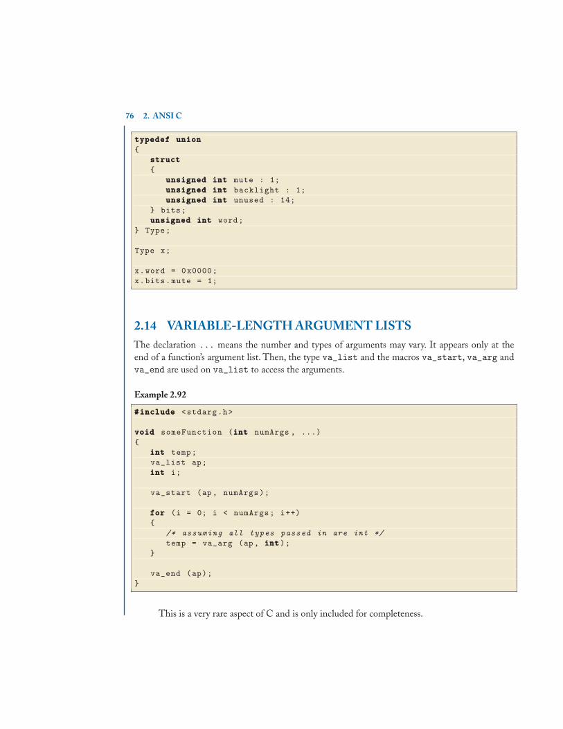
76 2. ANSI C
typedeftypedeftypedef unionunionunion{
structstructstruct{
unsignedunsignedunsigned intintint mute : 1;unsignedunsignedunsigned intintint backlight : 1;unsignedunsignedunsigned intintint unused : 14;
} bits;unsignedunsignedunsigned intintint word;
} Type;
Type x;
x.word = 0x0000;x.bits.mute = 1;
2.14 VARIABLE-LENGTH ARGUMENT LISTSThe declaration ... means the number and types of arguments may vary. It appears only at theend of a function’s argument list. Then, the type va_list and the macros va_start, va_arg andva_end are used on va_list to access the arguments.
Example 2.92
###includeincludeinclude <stdarg.h>
voidvoidvoid someFunction (intintint numArgs , ...){
intintint temp;va_list ap;intintint i;
va_start (ap, numArgs);
forforfor (i = 0; i < numArgs; i++){
/* assuming all types passed in are int */temp = va_arg (ap, intintint);
}
va_end (ap);}
This is a very rare aspect of C and is only included for completeness.
2.14. VARIABLE-LENGTH ARGUMENT LISTS 77
SUMMARYThis chapter has been a brief, yet complete presentation of the ANSI C high-level programminglanguage. It truly is one of the most valuable tools that an electrical or computer engineer canhave in their toolset going into the industry. It is a foundational language at the core of manyrecent derivative languages including C++, Microsoft’s C# and Apple’s Objective C. More relevantis the pervasiveness of C in so many embedded systems ranging from simple 8-bit microcontrollers,such as the ATMEL ATmega328P in an Arduino development board, to highly complex 32-bitmicroprocessors like the Texas Instruments OMAP dual core running embedded Linux Real TimeOperating Systems, which are written in C. C has been relevant for over 40 years and shows no realsign of disappearing.

79
C H A P T E R 3
Introduction to Arduino
3.1 BACKGROUND
The next topic we need to cover is our tool suite. In particular, we need a means for writing programsthat run on an embedded processor. This brings us to an Arduino, which refers to a circuit boardcontaining an ATMEL ATmega microcontroller preloaded with a boot loader program. A boot loaderis a tiny program (e.g., 2 Kbytes on the Arduino) stored in non-volatile memory at a location suchthat when power is applied or the reset button is pressed the CPU jumps into it and executes itsinstructions. The system is designed such that when the board is reset, the boot loader configuresthe microcontroller serial port to send and receive information to and from your computer, oftenreferred to as the host. Then, when you create an application, an embedded program you create to dosomething meaningful, you can send it to the target processor by uploading it. When you start theupload process, a special signal on the Arduino hardware causes the microcontroller to reset whichforces the boot loader to run. At that time, the boot loader is written such that it doesn’t assumeanything about the current state of the processor. So, it performs several steps to configure thecontroller to listen for incoming data on its serial communications port. Because the host computerinitiated an upload of the application program which caused the reset, there is data being sent via theserial port. So the boot loader sees this data and responds by saving it to the non-volatile memoryat a special location. When finished, the boot loader jumps to that application location in the flashand starts executing program instructions. In the event that the Arduino is manually reset or whenpower is first applied, the boot loader will not see any data on the serial port, and it will just jumpto the application location in flash. In either case, the boot loader jumps into your program whichdoes whatever it is you meant it to do.
A significant concept behind the Arduino embedded development platform is its intent ofbeing as open as possible. This means the hardware schematics of the circuit board (see Apx. A)are freely available in the public domain such that end users and, in particular, engineering studentscan create their own design beginning with an inexpensive functional platform. Additionally, theArduino Integrated Development Environment (IDE), a program that runs on your computer inorder to write and compile source-code into ATmega executable programs, is written in Java. Thebenefit of a Java-based IDE is that any computer with a Java interpreter is able to run the Arduinodevelopment software. In particular, students with Windows, MacOSX or even Linux will be ableto write programs for their embedded hardware.
The final component of Arduino is a library of functions referred to as Wiring. Any programdeveloped in the Arduino IDE is called a sketch.The concepts of Wiring and sketches are to benefit the

80 3. INTRODUCTION TO ARDUINO
end user by concealing all of the low-level details required to control the embedded microcontroller.While this is a meant to be a nice feature of using an Arduino, it is considered a negative in thisbook. The primary purpose of this text is to learn how to manipulate generic microcontrollers.We happen to be using the ATMEL ATmega328P microcontroller, which is the controller on anArduino development board. It is not useful to memorize the various Wiring functions, as they onlypertain to the ATmega processor as it sits on the Arduino circuit board. The significance of this isthat if you write a program using the Wiring library functions to do something interesting on theArduino hardware, it will not function on any other hardware platform. While it might be satisfyingto write software that causes the Arduino to do something, if it is not portable to another platform,then you have really limited your own usefulness in the engineering industry.
To correct this, we will avoid Wiring functions at all costs. Instead, we are going to usethe Arduino hardware and the IDE in order to learn how to develop ANSI C programs thatwill configure and control our embedded microcontroller. The methods introduced in subsequentchapters are meant to be universal and generic whenever possible.We will use a few Wiring functionsearly on out of necessity. In particular, the delay() and Serial functions will be used in manyapplications until much later when timers, interrupts and serial communication topics are all studied.Beyond this, the ANSI C methods presented are 100% portable, and the various topics covered areas generic as possible. Once learned, the end user only needs to refer to a microcontroller referencemanual to determine specific control over their target processor.
3.2 EXPERIMENTS USING THE ARDUINO DUEMILANOVEDEVELOPMENT BOARD
All of the material presented in this book will involve analyzing and developing embedded sourcecode that is run on the ATMEL ATmega328P microcontroller that sits on the Arduino Duemilanove(i.e., “2009” in Italian) development board as depicted in the modified photograph of Fig. 3.1. Manytimes, the C and assembly source code will be provided to allow readers to experiment with embeddedprogramming and applications.
The Arduino Duemilanove development board has an ATMEL ATmega328P 8-bit processoroperating at 16 MHz, with 2 Kbytes of SRAM, 32 Kbytes of Flash memory (2 Kbytes are alreadyused by the built-in boot loader, so only 30 Kbytes are available for your applications), 1 Kbyte ofElectrically-Erasable/Programmable Read-Only Memory (EEPROM ), three user accessible LEDs,and 20 input/output (I/O) pins; six of which provide Pulse-Width Modulation (PWM) analogoutput and six other provide Analog-to-Digital Converted (ADC) input. Many of these featuresare depicted on the modified photograph in Fig. 3.1.
The development board also provides a USB interface that allows for communication betweenthe ATmega328P and the Java-based IDE. So, for the lab work, we will always communicate withthe ATmega328P via the USB connector, at which time the development board also receives its 5 Vregulated power.However,note that there is also a 2.1 mm center-positive barrel power interface withassociated voltage regulator. Once a program is stored in the flash memory of the microcontroller, a

3.3. ARDUINO TOOLS TUTORIAL 81
Power LED
PORTD[7:0]PORTB[5:0]
PORTC[5:0]
Reset Button
ICSP Header
ATMEL ATmega328P
FTDI USB to RS232
DC Power
USB Connector
LED onPORTD[1]/RS232 Tx
LED onPORTB[5]
LED onPORTD[0]/RS232 Rx
VoltageRegulator
Crystal
External Power
SuppliedGNDRegulated
3.3V, 5V
Reset
Figure 3.1: Photograph of the Arduino Duemilanove development board, including key componentidentifications. Adapted from Arduino (2010).
separate DC power supply can be used to supply power to the board, at which time the built-in bootloader will run, ultimately jumping into whatever program is present. The Arduino Duemilanovecircuit board is designed to automatically switch to the correct power supply. If desired, power mayalso be supplied to the GND and Vin pins on the POWER header. The development board cansafely operate on an external supply of 7 V to 12 V.
3.3 ARDUINO TOOLS TUTORIAL
The purpose of this section is to ensure your embedded development environment is installed andready to go.
1. Download the latest Arduino IDE from http://arduino.cc/en/Main/Software. This isthe Java program used to create, write, compile and upload the embedded software.

82 3. INTRODUCTION TO ARDUINO
2. Download the latest Serial-to-USB drivers from http://www.ftdichip.com/Drivers/VCP.htm.These drivers allow for RS-232 serial communications via your computer’s USB port.Once installed, they create a virtual serial port, so the IDE is able to connect to the Arduinohardware via a physical USB cable. The driver converts USB communications to and from aserial protocol, so the IDE sends and received RS-232 data as though you had a serial port onyour computer (i.e., many modern computer manufacturers no longer provide serial ports).TheArduino circuit board includes an FTDI chip that performs a similar conversion between USBcommunications and RS-232 serial communications for the ATmega328P microcontroller.
3. Then:
• MacOSX: Install the USB drivers. Then connect the development board via the USBcable.
• Windows: Connect the development board via the USB cable. When prompted, installthe USB drivers.
4. The green power LED should light up. Additionally, if you have a new board, the yellow LED(connected to PortB[5]) should blink due to the pre-loaded application stored in the flash.
5. Then:
• MacOSX: Copy the Arduino IDE application to the Applications directory. Launch theArduino IDE.
• Windows: Open the Arduino folder and launch the Arduino IDE.
6. You should see a windows similar to that depicted in Fig. 3.2.
7. Open the example “Blink” program by selecting File→Examples→Digital→Blink.
8. You should have the following source code listing in an editor pane. Note that text in between/* */ is considered a comment for humans to document some important information regard-ing the program; that is, it is not actually part of the code used by the processor, and so it isomitted here. Also, all text on the same line following // is considered a comment and so isomitted here.
intintint ledPin = 13;
voidvoidvoid setup(){
pinMode(ledPin , OUTPUT);}
voidvoidvoid loop(){
digitalWrite(ledPin , HIGH);
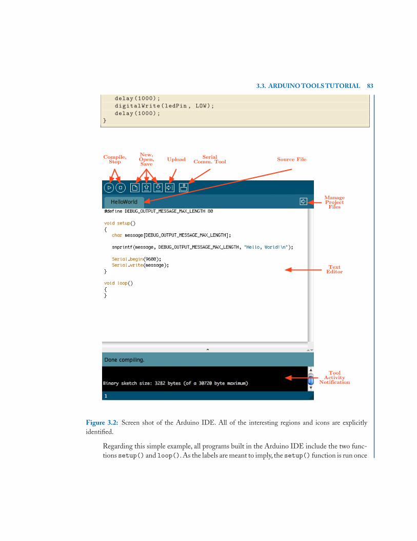
3.3. ARDUINO TOOLS TUTORIAL 83
delay (1000);digitalWrite(ledPin , LOW);delay (1000);
}
Compile,Stop
New, Open, Save
Upload Serial Comm. Tool Source File
Manage Project Files
Text Editor
Tool Activity
Notification
Figure 3.2: Screen shot of the Arduino IDE. All of the interesting regions and icons are explicitlyidentified.
Regarding this simple example, all programs built in the Arduino IDE include the two func-tions setup() and loop(). As the labels are meant to imply, the setup() function is run once
84 3. INTRODUCTION TO ARDUINO
when the program begins, so various initialization would take place here, while the loop()function executes over and over until the processor is reset. Imagine a race-car on an ovalrace-track; the car just keeps driving around the same loop until the race is finished. Thisexample includes a named piece of memory called a global variable, with the label ledPin.When the program is compiled on the host computer, this particular location in the targetmemory is initialzied with the value 13 because the Arduino circuit board’s 13th I/O pin hasthe yellow LED attached to it; see Apx. A. When setup() is run at the start of the program,a single library call is made to make the 13th I/O pin, referenced via that named variable, asan output pin, so that the processor can drive the line running to the LED either high or low,hence turning the LED on or off. Pins could be made to be input, so that a sensor or buttoncan be read in, instead. After setup() is finished, loop() is called over and over. Withinthe loop() function, the LED is turned on, and then a fixed delay of 1000 milliseconds isexecuted before the LED is turned off, and another delay.
Notice that none of the functions presented in this example are either assembly nor are theyANSI C; instead, they are all part of the provided Wiring library of functions.
9. With the “Blink” program in the editor, press the “play” icon in order to compile the program(the tool refers to this as “Verify”).
10. To upload the program to the embedded processor, first make sure you have the correct de-velopment board by checking under Tools→Board. It is most likely set to the correct valueof Arduino Duemilanove or Nano w/ ATmega328. If you have a different board, you shouldadjust accordingly.
11. Next, connect to the proper serial port under Tools→Serial Port
• MacOSX: /dev/tty.usbserial- (something)
• Windows: USB Serial (COMx); check device manager
In either case, the driver you installed earlier is allowing the development environment tocommunicate to the embedded processor with RS-232 serial communications via the USBcable.
12. Press the penultimate icon, the tool refers to this as “Upload”. You should see the Rx and Txyellow LEDs flash as the program is sent to the target flash memory. When it finishes, youshould see the LED blink at one second rate.
13. Now that you have compiled and uploaded your first program, let’s convert it from the easy-to-use-yet-non-standard library calls to easy-once-you-know-them-and-portable ANSI Cinstructions. Change the “Blink” program to the following.
voidvoidvoid MyDelay(unsignedunsignedunsigned longlonglong mSecondsApx);
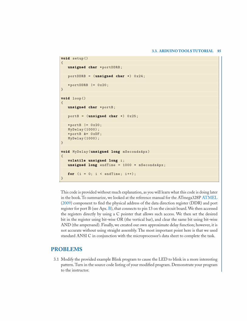
3.3. ARDUINO TOOLS TUTORIAL 85
voidvoidvoid setup(){
unsignedunsignedunsigned charcharchar *portDDRB;
portDDRB = (unsignedunsignedunsigned charcharchar *) 0x24;
*portDDRB |= 0x20;}
voidvoidvoid loop(){
unsignedunsignedunsigned charcharchar *portB;
portB = (unsignedunsignedunsigned charcharchar *) 0x25;
*portB |= 0x20;MyDelay (1000);*portB &= 0xDF;MyDelay (1000);
}
voidvoidvoid MyDelay(unsignedunsignedunsigned longlonglong mSecondsApx){
volatilevolatilevolatile unsignedunsignedunsigned longlonglong i;unsignedunsignedunsigned longlonglong endTime = 1000 * mSecondsApx;
forforfor (i = 0; i < endTime; i++);}
This code is provided without much explanation, as you will learn what this code is doing laterin the book. To summarize, we looked at the reference manual for the ATmega328P ATMEL(2009) component to find the physical address of the data direction register (DDR) and portregister for port B (see Apx. B), that connects to pin 13 on the circuit board. We then accessedthe registers directly by using a C pointer that allows such access. We then set the desiredbit in the register using bit-wise OR (the vertical bar), and clear the same bit using bit-wiseAND (the ampersand). Finally, we created our own approximate delay function; however, it isnot accurate without using straight assembly. The most important point here is that we usedstandard ANSI C in conjunction with the microprocessor’s data sheet to complete the task.
PROBLEMS
3.1 Modify the provided example Blink program to cause the LED to blink in a more interestingpattern. Turn in the source code listing of your modified program. Demonstrate your programto the instructor.

86 3. INTRODUCTION TO ARDUINO
3.2 State the total number of bytes required by your program in (3.1). Hint: this number is easilyobtained after you compile your program in the bottom window of the editor.
3.3 Modify the ANSI C version of the Blink program to cause the LED to blink in a moreinteresting pattern. Turn in the source code listing of your modified program.
3.4 State the total number of bytes required by your program in (3.3). Hint: this number is easilyobtained after you compile your program in the bottom window of the editor.

87
C H A P T E R 4
Embedded Debugging
4.1 INTRODUCTIONIn many ways, software development is universal among all levels of programs. From high-levelhost applications to low-level embedded routines. In particular, by using a high-level programminglanguage, engineers gain a great deal of portability that may lead to code re-use, and they gain ahigh-degree of maintainability through the proper use of self-documenting code constructs. Allsoftware development platforms, i.e., the CAD tools, include a compiler for the high-level language,an assembler for the architecture-specific language, and a linker to map software to physical or virtualaddresses within the target environment. Additionally, most software development platforms includea “design entry” tool that allows the engineer the ability to create the source code text files. This toolturns out to be de-coupled from the CAD suite, as often engineers will discover a particular editorprogram they like and will tend to use it separate from the actual compilation tool-chain.
Another very important aspect to the software development process is the ability for anengineer to test the correctness of their software design. It turns out there are several stages withinthe development process in which problems may occur with the design.The two broadest categoriesfor software defects include compile-time errors, in which the compiler is unable to successfully parsethe input text file, and run-time errors, in which an executable was created but the desired behavioris incorrect. The term bug, referring to an incident in the 1940’s in which a moth was caught in acomputer circuit resulting in a malfunction, is used to describe any unwanted behavior in a softwaredesign. As such, the process of attempting to resolve problems in software is called debugging. Somesoftware CAD tools include a debugger which is another program in the suite that allows an engineerthe ability to:
• halt program execution when a specific line of code is reached (i.e., breakpoints);
• once halted, look at the current contents of memory (i.e., memory watches);
• once halted, look at the current contents of CPU registers;
• receive notification of critical exceptions with explanations of the offending instruction;
• execute one instruction (both high-level and assembly) and then halting again (i.e., stepping);
• resume normal execution;
among many other useful abilities. For anyone who has developed PC application software, it seemslike the debugger is always present in the CAD tool-chain. For example, any of the Microsoft Visual
88 4. EMBEDDED DEBUGGING
Studio development environments tie their debugger into their editor, so the software developer canmake changes to their code, set breakpoints on certain lines, compile and run. The massive benefitoccurs when a breakpoint line is reached, execution of the program is halted and the debugger showsthe current line in the editor software. At this point, the developer can look at variable values, amongother things, and then continue execution in many ways.
The debug tool is extremely useful in the process of software development. The observantreader would have noticed that the debugger is available to the PC application developer becausethe source code is compiled, assembled and linked for the same processor architecture as that ofthe CAD tools themselves. This means that the source code is able to include special debug markerinformation, so the debug tool can follow along with how the application is running. Additionally,the debug tool is able to see the state of registers and memory because the software in questionis running on the same processor as the debugger. Unfortunately, this is not possible with cross-compilers, in which software is compiled, assembled and linked into a target architecture other thanthat of the host computer. In fact, this is the very nature of embedded development – we have tocreate software on a host computer, and then compile, assemble and link into a target architecture.It is not possible for a debugger on a host to see what is taking place inside a target processor.
As a result, some embedded debugging tools are available, especially for large microprocessors.Often they involve an intermediate device, i.e,.hardware debugger or emulator, such as those depictedin Fig. 4.1, between the host and the target processors.
Such a hardware debugger usually has a second microprocessor inside that is able to understandthe same machine instructions as that of the target processor. Additionally, the target architecturehas to provide the ability to allow the debugger to halt its program counter and look at registers andmemory, etc. The host debugging software tool then communicates with the hardware debugger inorder to perform the same kind of debugging abilities as that previously stated for the application-level development environment.
While a hardware debugger is a great tool to have, it is not always available for all platforms.In particular, often smaller microcontrollers will not have such devices available (although it neverhurts to check on this at the start of a new project!). Additionally, hardware debuggers can addsignificant cost to a project and may not always fit into a small budget. And so, engineers have toresort to simpler methods for debugging their software. For anyone who has developed PC consoleapplication software, the idea is to add temporary output instructions that are removed once theprogram is working as desired. Typically, the standard C function printf() (see Sec. 2.3) is used toprint text, possibly containing current memory values, to the console (i.e., output terminal). Again,the observant reader would have noticed that most embedded platforms do not have a convenientstandard-output console. Fortunately, many embedded processors do have at least one serial dataport, which will often be used during development for which the embedded software can dumpinformation; this is the case for the Arduino development board. In the event that no console isavailable at all, the most common method for embedded debugging is toggling a general I/O portpin between ‘1’ and ‘0’ which can be observed either via an LED or an oscilloscope. It turns out
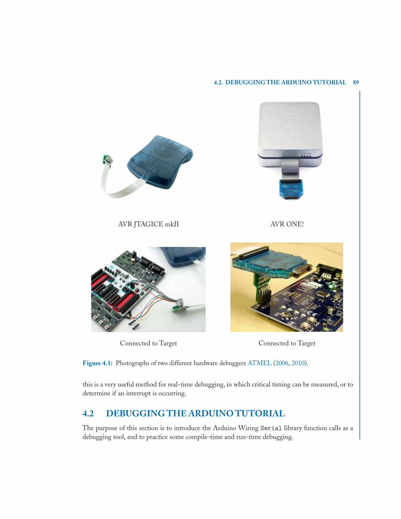
4.2. DEBUGGING THE ARDUINO TUTORIAL 89
AVR JTAGICE mkII AVR ONE!
Connected to Target Connected to Target
Figure 4.1: Photographs of two different hardware debuggers ATMEL (2006, 2010).
this is a very useful method for real-time debugging, in which critical timing can be measured, or todetermine if an interrupt is occurring.
4.2 DEBUGGING THE ARDUINO TUTORIAL
The purpose of this section is to introduce the Arduino Wiring Serial library function calls as adebugging tool, and to practice some compile-time and run-time debugging.

90 4. EMBEDDED DEBUGGING
1. Visit http://arduino.cc/en/Reference/Serial to review the Arduino Serial libraryfunctions begin(), and write().
2. Use the Serial.begin() and Serial.write() methods to complete the following “Hello,World!” program. Note that the C function snprintf() is the same as printf(), except itprints a formatted string to a memory buffer instead of the standard output port. So, you cando any sort of printing to our serial console by first printing to a buffer and then writing thebuffer out the serial port.
###definedefinedefine DEBUG_OUTPUT_MESSAGE_MAX_LENGTH 80
voidvoidvoid setup(){
charcharchar message[DEBUG_OUTPUT_MESSAGE_MAX_LENGTH ];
snprintf(message , DEBUG_OUTPUT_MESSAGE_MAX_LENGTH , "Hello ,World!\n");
}
voidvoidvoid loop(){}
3. Compile and upload your program to the development board. Open the serial monitor, resetyour board and enjoy your first program. Tip: make sure that the baud rate you use in theSerial.begin() method is the same as your serial monitor setting. You can change the baudrate to any of the acceptable values; the boot loader will always reset the serial port so you cancontinue downloading new programs later.
PROBLEMS4.1 Practice compile-time debugging by fixing all of the syntax errors in the following listing.
Do yourself a favor and work through all the bugs using the Arduino IDE compile outputinformation. Turn in the source code listing of your debugged program. Clearly state all of thesyntax errors that you found.
voidvoidvoid MyDelay(unsignedunsignedunsigned longlonglong mSecondsApx);
voidvoidvoid setup(){
unsignedunsignedunsigned charcharchar *portDDRB;
portDDRB = (unsignedunsignedunsigned charcharchar *) 0x24;
*portDDRB |= Ox2O;

4.2. DEBUGGING THE ARDUINO TUTORIAL 91
}
voidvoidvoid loop(){
unsignedunsignedunsigned charcharchar *portB;
portB = (unsignedunsignedunsigned charcharchar *) 0x25;
*portB |= Ox2O;MyDelay {1000}*portB &= OxDF:MyDelay [1000] ,
}
voidvoidvoid MyDelay(unsignedunsignedunsigned longlonglong mSecondsApx){
volatilevolatilevolatile unsignedunsignedunsigned longlonglong i;unsignedunsignedunsigned longlonglong endTime = 1000 * mSecondsApx;
forforfor (i = 0; i < endTime; i++);}
4.2 Practice run-time debugging by fixing the following listing, so that the LED will blink like itwas meant to. Note: you should be able to do this with two minor changes.
voidvoidvoid NewDelay(unsignedunsignedunsigned charcharchar mSecondsApx);
voidvoidvoid setup(){
unsignedunsignedunsigned charcharchar *portDDRB;
portDDRB = (unsignedunsignedunsigned charcharchar *) 0x24;
*portDDRB |= 0x20;}
voidvoidvoid loop(){
unsignedunsignedunsigned charcharchar *portB;
portB = (unsignedunsignedunsigned charcharchar *) 0x25;
*portB |= 0x20;NewDelay (100);*portB &= 0xDF;NewDelay (100);
}
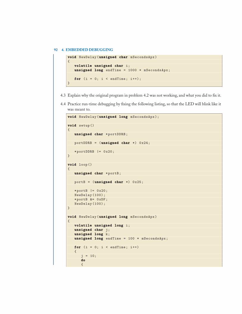
92 4. EMBEDDED DEBUGGING
voidvoidvoid NewDelay(unsignedunsignedunsigned charcharchar mSecondsApx){
volatilevolatilevolatile unsignedunsignedunsigned charcharchar i;unsignedunsignedunsigned longlonglong endTime = 1000 * mSecondsApx;
forforfor (i = 0; i < endTime; i++);}
4.3 Explain why the original program in problem 4.2 was not working, and what you did to fix it.
4.4 Practice run-time debugging by fixing the following listing, so that the LED will blink like itwas meant to.
voidvoidvoid NewDelay(unsignedunsignedunsigned longlonglong mSecondsApx);
voidvoidvoid setup(){
unsignedunsignedunsigned charcharchar *portDDRB;
portDDRB = (unsignedunsignedunsigned charcharchar *) 0x24;
*portDDRB |= 0x20;}
voidvoidvoid loop(){
unsignedunsignedunsigned charcharchar *portB;
portB = (unsignedunsignedunsigned charcharchar *) 0x25;
*portB |= 0x20;NewDelay (100);*portB &= 0xDF;NewDelay (100);
}
voidvoidvoid NewDelay(unsignedunsignedunsigned longlonglong mSecondsApx){
volatilevolatilevolatile unsignedunsignedunsigned longlonglong i;unsignedunsignedunsigned charcharchar j;unsignedunsignedunsigned longlonglong k;unsignedunsignedunsigned longlonglong endTime = 100 * mSecondsApx;
forforfor (i = 0; i < endTime; i++){
j = 10;dododo{
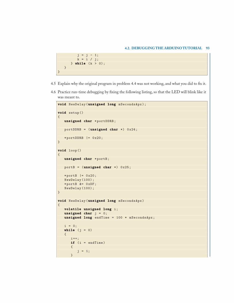
4.2. DEBUGGING THE ARDUINO TUTORIAL 93
j = j - 1;k = i / j;
} whilewhilewhile (k > 0);}
}
4.5 Explain why the original program in problem 4.4 was not working, and what you did to fix it.
4.6 Practice run-time debugging by fixing the following listing, so that the LED will blink like itwas meant to.
voidvoidvoid NewDelay(unsignedunsignedunsigned longlonglong mSecondsApx);
voidvoidvoid setup(){
unsignedunsignedunsigned charcharchar *portDDRB;
portDDRB = (unsignedunsignedunsigned charcharchar *) 0x24;
*portDDRB |= 0x20;}
voidvoidvoid loop(){
unsignedunsignedunsigned charcharchar *portB;
portB = (unsignedunsignedunsigned charcharchar *) 0x25;
*portB |= 0x20;NewDelay (100);*portB &= 0xDF;NewDelay (100);
}
voidvoidvoid NewDelay(unsignedunsignedunsigned longlonglong mSecondsApx){
volatilevolatilevolatile unsignedunsignedunsigned longlonglong i;unsignedunsignedunsigned charcharchar j = 0;unsignedunsignedunsigned longlonglong endTime = 100 * mSecondsApx;
i = 0;whilewhilewhile (j = 0){
i++;ififif (i = endTime){
j = 1;}

94 4. EMBEDDED DEBUGGING
}}
4.7 Explain why the original program in problem 4.6 was not working, and what you did to fix it.

95
C H A P T E R 5
ATmega328P ArchitectureBefore we can learn how to control peripheral devices in general, we need to understand how ourspecific microcontroller is structured and functions. This is typically referred to as its architecture.The schematic of the Arduino in Apx. A shows the ATMEL ATmega328P microcontroller is atthe heart of the development board. This brief chapter is meant to introduce the basic structureand operation of the microcontroller with specific emphasis on the AVR CPU. Most informationpresented within this chapter comes directly from ATMEL (2009).
5.1 OVERVIEW
The ATmega328P is a low-power CMOS 8-bit microcontroller based on the AVR enhanced Re-duced Instruction Set Computing (RISC) architecture. A simplified block diagram containing themost pertinent components of the ATmega328P microcontroller is presented in Fig. 5.1.
The ATmega328P provides the following significant features: 32 KBytes of In-System Pro-grammable (ISP) flash to store programs, 2 KBytes SRAM to hold run-time variables, 1 KBytesEEPROM to store any data that programs may wish to retain after power is cycled, 23 general pur-pose input/output (GPIO) lines, 32 general purpose working registers, three Timer/Counters withcompare modes, internal and external interrupts, a Universal Synchronous/Asynchronous Receiver/-Transmitter (USART), a 2-wire Serial Interface (TWI) serial port, a Serial Peripheral Interface (SPI)serial port, and a 6-channel 10-bit Analog/Digital Converter (ADC).
All of these peripheral devices are controlled via sets of specific registers, each of whichis connected to the 8-bit data bus. Thus, a program interacts with each peripheral by accessingvarious memory-mapped registers, for example via C pointers. Additionally, each peripheral deviceaccesses the off-chip pins via one of the three available ports B, C or D. Each port is configurablevia memory-mapped registers to allow different functions access to external pins; a process calledpin-multiplexing.
The on-chip ISP flash allows the program memory to be changed via either a SPI serialinterface, a conventional non-volatile memory programmer, or an on-chip boot loader running onthe AVR core. Note that the latter method is that used by the Arduino IDE.The boot loader can useany interface to download the application program in the application flash memory. The Arduinoboot loader uses the USART configured for RS-232 via the USB-to-serial converter chip on thedevelopment board. Software in the boot flash section will continue to run while the applicationflash section is updated. By combining an 8-bit RISC CPU with ISP flash on a monolithic chip,
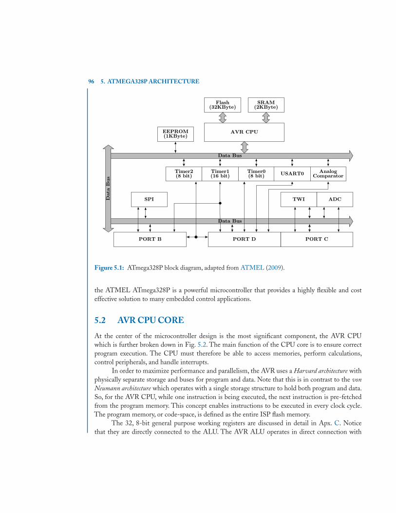
96 5. ATMEGA328P ARCHITECTURE
AVR CPU
Flash(32KByte)
SRAM(2KByte)
EEPROM(1KByte)
Timer1(16 bit)
Timer0(8 bit)
Timer2(8 bit)
ADC
Data Bus
Data Bus
AnalogComparatorUSART0
SPI TWI
PORT B PORT CPORT D
Data
Bus
Figure 5.1: ATmega328P block diagram, adapted from ATMEL (2009).
the ATMEL ATmega328P is a powerful microcontroller that provides a highly flexible and costeffective solution to many embedded control applications.
5.2 AVR CPU CORE
At the center of the microcontroller design is the most significant component, the AVR CPUwhich is further broken down in Fig. 5.2. The main function of the CPU core is to ensure correctprogram execution. The CPU must therefore be able to access memories, perform calculations,control peripherals, and handle interrupts.
In order to maximize performance and parallelism, the AVR uses a Harvard architecture withphysically separate storage and buses for program and data. Note that this is in contrast to the vonNeumann architecture which operates with a single storage structure to hold both program and data.So, for the AVR CPU, while one instruction is being executed, the next instruction is pre-fetchedfrom the program memory. This concept enables instructions to be executed in every clock cycle.The program memory, or code-space, is defined as the entire ISP flash memory.
The 32, 8-bit general purpose working registers are discussed in detail in Apx. C. Noticethat they are directly connected to the ALU. The AVR ALU operates in direct connection with

5.2. AVR CPU CORE 97
Data Bus
Data
Bus
PC SREG
32 General Purpose Registers (8-bit)
ALU
SRAM(2KByte)
Flash(32KByte)
InstructionRegister
InstructionDecoder
Control Lines
Indir
ect
Addre
ssin
g
Dir
ect
Addre
ssin
g
Figure 5.2: AVR CPU block diagram, adapted from ATMEL (2009).
all the 32 general purpose working registers. Within a single clock cycle, arithmetic operationsbetween general purpose registers or between a register and an immediate are executed. The ALUoperations are divided into the three main categories arithmetic, logical, and bit-functions. After anarithmetic operation, the status register (SREG) is updated to reflect information about the resultof the operation. The SREG is described in full detail in Apx. C.
Six of the 32 registers can be used as three 16-bit indirect address register pointers for dataspace addressing, enabling efficient address calculations. One of the these address pointers can alsobe used as an address pointer for look up tables in flash program memory. These added functionregisters are the 16-bit X-, Y-, and Z-registers, described in more detail in Apx. C.
Program flow is provided by conditional and unconditional jump and call instructions, able todirectly address the whole address space. Most AVR instructions have a single 16-bit word format.Every program memory address contains a 16- or 32-bit instruction.
During interrupts and subroutine calls, the return address Program Counter (PC) is storedon the stack. The stack is effectively allocated in the general data SRAM, and, consequently, the

98 5. ATMEGA328P ARCHITECTURE
stack size is only limited by the total SRAM size and the usage of the SRAM. All user programsmust initialize the SP in the reset routine before subroutines or interrupts are executed. The StackPointer (SP) is read/write accessible in the I/O space and is described in greater detail in Apx. C.The data SRAM can easily be accessed through the five different addressing modes supported inthe AVR architecture.
SUMMARYThe Arduino development board contains an ATMEL ATmega328P microcontroller as its embed-ded controlling device.The material presented in this brief chapter was meant to introduce the basicfunctionality and operation of the processor. In particular, the block diagrams in Fig. 5.1 and Fig. 5.2will be frequently referred to in subsequent chapters when introducing the various peripheral devices.You will see a recurring pattern when configuring the various peripherals. In particular, each on-chipperipheral device has its own set of registers. Each register is memory-mapped, and so connected tothe 8-bit data bus. When the program needs to access a peripheral, all it needs to do is access theregisters via their address, then set and clear the bits to achieve the desired configurations.

99
C H A P T E R 6
General-Purpose Input/Output
6.1 OUTPUT6.1.1 INTRODUCTIONThe most commonly used microprocessor component within embedded systems is probably the setof general-purpose input/output (GPIO) ports. As the name implies, these hardware componentsprovide a very generic interface to external peripheral devices in the form of individual digital lines.Each GPIO line has a pathway from the microcontroller integrated circuit (IC) to an external pinon the microcontroller package. As a result, GPIO lines can be connected to any device that cansource or sink digital signals (e.g., buttons or LEDs), and software can be written to directly controlwhether the pin outputs a ‘1’ or ‘0’ or reads digital values as an input pin.
6.1.2 BASIC OPERATIONShown in Fig. 6.1 is a stripped-down schematic of a single port pin on the ATmega328P containingonly the Data Direction Register (DDR) bit and the data bit. While this circuitry is specific tothe ATmega328P processor, it represents very typical architecture to most microprocessors andmicrocontrollers. That is, it is very common for a microprocessor to provide bi-directional GPIOlines for generic usage within embedded systems.This schematic details GPIO pin n on port x. Fromthe simplified figure, there are two D flip-flop memory elements for each GPIO line.The bottom Dflip-flop stores whatever value is on line Portx_Bitn when the control signal WritePortx_Bitngoes from low to high; this will occur by the CPU generating the appropriate signals when theprogram executes an instruction to write to this particular register. In a similar sense, the top Dflip-flop stores the value present on DDRx_Bitn when the control signal WriteDDRx_Bitn occurs.The three tri-state buffers allow their input signals to pass when enabled; otherwise, they present ahigh-impedance state to the output (i.e., disconnecting the line from the output).
So, the basic operation to output a digital signal on pin n of port x is to:
1. write a ‘1’ into DDRx_Bitn, then
2. write either a ‘1’ or ‘0’ into Portx_Bitn.
The first step results in enabling the tri-state buffer connecting the output of the bottom D flip-flopto the actual pin going off-chip. The second step stores whatever signal is desired which will bepassed through the tri-state buffer to the pin. This configuration makes the port pin an output, asthe CPU is now free to store ‘1’s and ‘0’s into the bottom D flip-flop, which will then always drive

100 6. GENERAL-PURPOSE INPUT/OUTPUT
PORT x
Data
Bus D Q
D Q
ReadDDRx_Bitn
DDRx_BitnWriteDDRx_Bitn
ReadPortx_Bitn
Portx_BitnWritePortx_BitnPortx_Pinn
AV
R C
PU
Figure 6.1: A schematic of a single port pin containing only the Data Direction Register (DDR) bitand the Data bit, adapted from ATMEL (2009).
the pin high or low. Note that if a ‘0’ is written into DDRx_Bitn, the tri-state buffer is disabled, andthe pin is no longer driven high or low; this will be revisited in Sec. 6.2. Finally, note the CPU isable to read the contents of both D flip-flops at any time by enabling the associated Readx_Bitncontrol lines, which will then pass the contents of either D flip-flop onto the data bus.
6.1.3 PIN-MUXINGOne complication with GPIO lines typical to most microprocessor architectures is the process calledpin-muxing. The idea is that microprocessors provide plenty of functionality on their tiny IC, buteach sub-system requires its own set of I/O pins necessary to drive the behavior. As a result, if amicroprocessor provided a unique pin for each signal possible, the package would grow to undesirablesize. Additionally, most applications do not make use of every on-chip peripheral device for theirspecific embedded system. Thus, manufacturers often if not always use multiplexers on pins in orderto share the pin among sub-systems. For example, if an embedded system calls for the processorto interface with peripheral device y, a couple of pins can be dedicated to its functionality, andso, they can not be used for GPIO. Usually, specific registers are used to control the pin-muxingconfiguration of the processor. On the ATmega328P, pin-muxing is as depicted in Fig. 6.2, in whichthe specific peripheral sub-systems will generate their own override signals in order to obtain controlof individual pins.

6.1. OUTPUT 101
PORT x
Data
Bus D Q
D Q
ReadDDRx_Bitn
DDRx_BitnWriteDDRx_Bitn
ReadPortx_Bitn
Portx_BitnWritePortx_Bitn Portx_Pinn
AV
R C
PU
Peripheral y
0
1
0
1
DDOVx_Bitn
DDOEx_Bitn
PortOVx_Bitn
PortOEx_Bitn
Figure 6.2: A schematic of a single port pin containing the DDR and Data bits with the addition ofpin-mux multiplexers, adapted from ATMEL (2009).
New to the schematic are two multiplexers, one for each D flip-flop output. Each multiplexerwill pass the D flip-flop value as long as the associated override enable line from peripheral y is‘0’ (i.e., PortOEx_Bitn and DDOEx_Bitn). When either line goes high, the corresponding D flip-flop value is blocked and replaced with the associated override value line from peripheral y (i.e.,PortOVx_Bitn and DDOVx_Bitn). In this way, if peripheral y ’s sub-circuitry is enabled, it willautomatically make use of the associated pins. To make use of GPIO lines, care must be taken toensure the muxed devices are turned off or disabled.
See Apx. A for a complete table of all GPIO port pins and their alternative functions viapin-muxing. In general, if the peripheral device is enabled, it will override the ability to use a pin asgeneral I/O.
The final step in understanding GPIO ports is handled by combining groups of pins intoregisters, as depicted in Figure 6.3. This figure details the fact that individual D flip-flops are notaddressable directly, but they are addressed in groups of a certain size. In the case of the ATmega328P,port registers are all accessed in eight-bit units. The primary change in the figure is the combinationof D flip-flops into 8-bit registers, all of which store their input bit values when the single control lineWriteDDRx or WritePortx goes from low to high. This is a significant point: in order to change asingle bit in a register, all seven other bits must also be written. The typical method for handling

102 6. GENERAL-PURPOSE INPUT/OUTPUT
PORT x
Data
Bus
ReadDDRx_Bit0
DDRx_Bit0
WriteDDRx
ReadPortx_Bit0
Portx_Bit0
WritePortx
Portx_Pin0
AV
R C
PU
Peripheral y
0
1
0
1
DDOVx_Bit0
DDOEx_Bit0
PortOVx_Bit0
PortOEx_Bit0
D0
D7
Q0
Q7
D0
D7
Q0
Q7
Figure 6.3: A schematic of an eight-bit port showing only a single DDR and Data bit with the additionof pin-mux multiplexers.
this issue is by first reading the current contents of the register, then masking the bit-of-interest,and finally writing the entire register back. While the process reads and writes the entire eight bits,only the bit-of-interest is changed.
Note for simplicity, the figure does not depict all tri-state buffers, multiplexers, nor pins; thereare eight instances of each.
6.2 INPUT6.2.1 INTRODUCTIONThis section continues exploring the most commonly used microprocessor component within em-bedded systems, the set of GPIO ports. By now, it is assumed the reader has already been introducedto GPIO port pins. In particular, the reader should be familiar with outputting logic-high and lowvalues on individual pins in order to drive peripheral devices, for example turning on and off an LED.Generally speaking, the two port registers that are most important for setting a port pin as an outputand then driving a value on that pin are the DDR and the Data register. For the ATmega328P, aport pin is configured as an output when a ‘1’ is written into the corresponding DDR bit position,
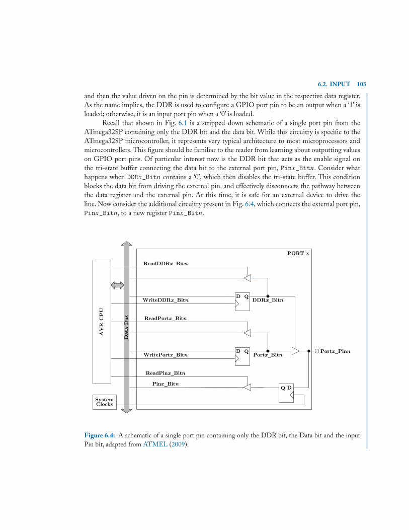
6.2. INPUT 103
and then the value driven on the pin is determined by the bit value in the respective data register.As the name implies, the DDR is used to configure a GPIO port pin to be an output when a ‘1’ isloaded; otherwise, it is an input port pin when a ‘0’ is loaded.
Recall that shown in Fig. 6.1 is a stripped-down schematic of a single port pin from theATmega328P containing only the DDR bit and the data bit. While this circuitry is specific to theATmega328P microcontroller, it represents very typical architecture to most microprocessors andmicrocontrollers. This figure should be familiar to the reader from learning about outputting valueson GPIO port pins. Of particular interest now is the DDR bit that acts as the enable signal onthe tri-state buffer connecting the data bit to the external port pin, Pinx_Bitn. Consider whathappens when DDRx_Bitn contains a ‘0’, which then disables the tri-state buffer. This conditionblocks the data bit from driving the external pin, and effectively disconnects the pathway betweenthe data register and the external pin. At this time, it is safe for an external device to drive theline. Now consider the additional circuitry present in Fig. 6.4, which connects the external port pin,Pinx_Bitn, to a new register Pinx_Bitn.
PORT x
Data
Bus
D Q
D Q
ReadDDRx_Bitn
DDRx_BitnWriteDDRx_Bitn
ReadPortx_Bitn
Portx_BitnWritePortx_BitnPortx_Pinn
AV
R C
PU
DQ
ReadPinx_Bitn
Pinx_Bitn
System Clocks
Figure 6.4: A schematic of a single port pin containing only the DDR bit, the Data bit and the inputPin bit, adapted from ATMEL (2009).

104 6. GENERAL-PURPOSE INPUT/OUTPUT
As can be seen from the figure, when the DDR contains a ‘0’, the tri-state buffer prevents theData bit from passing through, safely allowing an external device to drive the pin.The driving signal islatched into the new register, which can then be read by the CPU by simply accessing the appropriatebit out of the port Pin register.Note that this method is specific to the ATmega328P; many processorsre-use the data register for both outputting-from as well as inputting-to the microcontroller.
So, the basic operation to input a digital signal on pin n of port x is to:
1. write a ‘0’ into DDRx_Bitn, then
2. read the value out of Pinx_Bitn.
The first step results in disabling the tri-state buffer connecting the output of the data D flip-flop tothe actual pin going off-chip.The second step reads whatever signal is currently stored in the registerwhose input is connected directly to the pin. This configuration makes the port pin an input, as theCPU is now able to read ‘1’s and ‘0’s out of the bottom D flip-flop, which is constantly sampling theexternal pin via the control signal coming from the System Clocks sub-circuitry.
6.2.2 INTERNAL PULL-UP RESISTORGenerally, when a port pin is not being used, the microcontroller will default the pins to input, inorder to save on power. However, if the pin is unused, then it is probably not connected to any externalcircuitry. As a result, the input pin is floating, and the input signal to the Pinx_Bitn D flip-flop isunknown, which can lead to strange and unexpected behavior; for example, an unexpected/unwantedinterrupt might occur. A very standard method for managing unused input pins is to connect a fairlylarge resistance between the pin and the power supply. In this way, the port pin is very weakly pulledhigh, and no unwanted transitions will occur. It turns out that because this method is so standard,most microprocessors will provide internal pull-up resistors on any port pins that may be configuredas inputs.
The ATmega328P provides internal pull-up resistors on all port pins, which can be enabledand disabled based on the schematic depicted in Fig. 6.5. New to the schematic is an AND gatethat has inputs of the DDRx_Bitn output via an inversion and the Portx_Bitn output. The outputof the AND gate goes to the gate of a transistor, which then allows a channel pathway between thepower supply and the pin perhaps through a resistor, although the transistor can be made to act asthe resistor itself. As a result, an internal pull-up behavior is enabled via the following procedure:
1. write a ‘0’ into DDRx_Bitn, then
2. write a ‘1’ into Portx_Bitn.
To keep a port pin configured as an input,but to disable the internal pull-up,a ‘0’would be written intoPortx_Bitn instead. Note that this procedure is very specific to the ATmega328P microcontroller;other processors offer their own methods for managing internal pull-up resistors.

6.3. ACCESSING GPIO LINES IN C 105
PORT xD
ata
Bus
D Q
D Q
ReadDDRx_Bitn
DDRx_BitnWriteDDRx_Bitn
ReadPortx_Bitn
Portx_BitnWritePortx_BitnPortx_Pinn
AV
R C
PU
DQ
ReadPinx_Bitn
Pinx_Bitn
System Clocks
VDD
Figure 6.5: A schematic of a single port pin containing the DDR bit, the Data bit and the input Pin bitwith the addition of a pull-up resistor, adapted from ATMEL (2009).
6.3 ACCESSING GPIO LINES IN C6.3.1 MANAGING OUTPUTSThe first step for accessing GPIO lines in software is identifying the addresses at which the DDRand Data registers exist. In the case of the ATmega328P, three ports exist, PORTB, PORTC and PORTDall specified in Sec. 6.4. Note that PORTC only has seven bits available. From C, it is possible to readand write the contents of these registers using pointers to eight-bit elements as in the followingexample.
Example 6.1
unsignedunsignedunsigned charcharchar *portDDRB;
portDDRB = (unsignedunsignedunsigned charcharchar *) 0x24;
The lines in Ex. 6.1 declares a pointer variable that points to an eight-bit unsigned char,and then loads that pointer variable with the hard-coded value of the data-space address for the

106 6. GENERAL-PURPOSE INPUT/OUTPUT
desired register. Once the pointer is available, the register can be read-from and written-to by simplydereferencing the pointer.The final trick is in knowing how to access specific bits within the register.Suppose the program needs to clear bit 6 and set bit 5. The following example shows how to formthe proper bit-masks and the usage of bitwise AND and OR operations.
Example 6.2
###definedefinedefine BIT6_MASK 0x40 // 0100 0000###definedefinedefine BIT5_MASK 0x20 // 0010 0000
*someRegisterPointer = (* someRegisterPointer) & (˜ BIT6_MASK);*someRegisterPointer = (* someRegisterPointer) | BIT5_MASK;
The first line makes use of the ones’ complement of the bit mask to generate the bit vector10111111 which is then ANDed bit-per-bit along the contents of the register. The result, whichhas a ‘0’ forced into the sixth bit, is written back into the register. The second line simply performsa bitwise OR of the contents of the register with the bit vector 00100000, which results in setting a‘1’ into the fifth bit.
6.3.2 MANAGING INPUTSThere are two methods for managing GPIO input port pins in software, polling and usage ofinterrupts. Because interrupts are generally more problematic to work with, this topic will be deferredto a later chapter. Instead, the method of polling an input pin will be used to capture when an externalsignal changes.
6.3.2.1 PollingPolling is the simple process of repeatedly reading the value of the input pin(s) and comparing thecurrent value to the previously-read value to determine if an external signal event has occurred; i.e.,when a digital line switches states from ‘1’ to ‘0’ or ‘0’ to ‘1’. As was done for outputting on GPIOport pins, the first step for accessing GPIO inputs in software is identifying the addresses at whichthe DDR, Data and Pin registers exist.
In the case of the ATmega328P, three ports exist, PORTB, PORTC and PORTD all specified inSec. 6.4. From C, it is possible to configure a port pin as an input using pointers to eight-bit elementsas in the following example.
Example 6.3
unsignedunsignedunsigned charcharchar *portDDRB;unsignedunsignedunsigned charcharchar *portDataB;unsignedunsignedunsigned charcharchar *portPinB;
portDDRB = (unsignedunsignedunsigned charcharchar *) 0x24;

6.4. PERTINENT REGISTER DESCRIPTIONS 107
portDataB = (unsignedunsignedunsigned charcharchar *) 0x25;portPinB = (unsignedunsignedunsigned charcharchar *) 0x23;
The code in the previous example declares a pointer variable that points to an eight-bit unsignedchar, and then it loads that pointer variable with the hard-coded value of the data-space address
for the desired register. Now suppose the program needs to make bit 0 of port B an input with aninternal pull-up resistor enabled. The following example demonstrates.
Example 6.4
###definedefinedefine BIT0_MASK 0x01 // 0000 0001
*portDDRB = (* portDDRB) & (˜ BIT0_MASK); // configure bit 0 as an input*portDataB = (* portDataB) | BIT0_MASK; // turn on the bit 0 pull -up
resistor
The final step is to continuously sample the pin-of-interest, waiting for it to change. When a changeoccurs, the program can “do something”. Consider the following code piece that would sit in theloop() function of the Arduino sketch.
Example 6.5
voidvoidvoid loop(){
unsignedunsignedunsigned charcharchar previousSample;unsignedunsignedunsigned charcharchar currentSample;
currentSample = (* portPinB) & BIT0_MASK; // only interested in bit 0ififif (currentSample != previousSample){
// a change has occurred; we should do something}
// store the current sample as the next previous samplepreviousSample = currentSample;
}
Notice how this code doesn’t do anything interesting until a change is measured on the input portpin. It just keeps comparing the “previous sample” with the “current sample”. In this way, the softwareis sampling the input data and detecting when a signal event occurs.
6.4 PERTINENT REGISTER DESCRIPTIONSThe information presented in this section was taken from ATMEL (2009).

108 6. GENERAL-PURPOSE INPUT/OUTPUT
6.4.1 PORTB - THE PORT B DATA REGISTER
Bit 7 6 5 4 3 2 1 00x25 PORTB7 PORTB6 PORTB5 PORTB4 PORTB3 PORTB2 PORTB1 PORTB0
Read/Write R/W R/W R/W R/W R/W R/W R/W R/WDefault 0 0 0 0 0 0 0 0
• PORTB7-0: GPIO data value stored in bit n.
6.4.2 DDRB - THE PORT B DATA DIRECTION REGISTER
Bit 7 6 5 4 3 2 1 00x24 DDRB7 DDRB6 DDRB5 DDRB4 DDRB3 DDRB2 DDRB1 DDRB0
Read/Write R/W R/W R/W R/W R/W R/W R/W R/WDefault 0 0 0 0 0 0 0 0
• DDRB7-0: selects the direction of pin n. If DDRBn is written ‘1’, then PORTBn is configuredas an output pin. If DDRBn is written ‘0’, then PORTBn is configured as an input pin.
6.4.3 PINB - THE PORT B INPUT PINS ADDRESS
Bit 7 6 5 4 3 2 1 00x23 PINB7 PINB6 PINB5 PINB4 PINB3 PINB2 PINB1 PINB0
Read/Write R R R R R R R RDefault - - - - - - - -
• PINB7-0: logic value present on external pin n.
6.4.4 PORTC - THE PORT C DATA REGISTER
Bit 7 6 5 4 3 2 1 00x28 - PORTC6 PORTC5 PORTC4 PORTC3 PORTC2 PORTC1 PORTC0
Read/Write R R/W R/W R/W R/W R/W R/W R/WDefault 0 0 0 0 0 0 0 0
• PORTC6-0: GPIO data value stored in bit n.
6.4.5 DDRC - THE PORT C DATA DIRECTION REGISTER
Bit 7 6 5 4 3 2 1 00x27 - DDRC6 DDRC5 DDRC4 DDRC3 DDRC2 DDRC1 DDRC0
Read/Write R R/W R/W R/W R/W R/W R/W R/WDefault 0 0 0 0 0 0 0 0
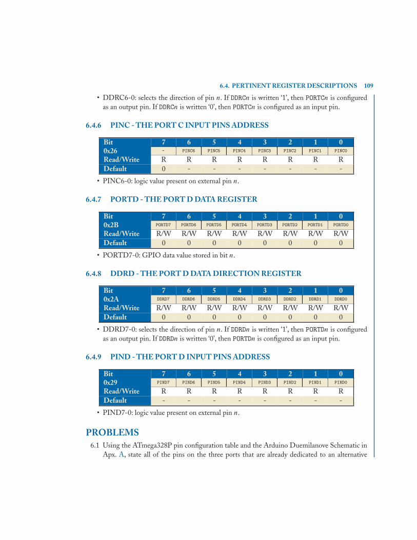
6.4. PERTINENT REGISTER DESCRIPTIONS 109
• DDRC6-0: selects the direction of pin n. If DDRCn is written ‘1’, then PORTCn is configuredas an output pin. If DDRCn is written ‘0’, then PORTCn is configured as an input pin.
6.4.6 PINC - THE PORT C INPUT PINS ADDRESS
Bit 7 6 5 4 3 2 1 00x26 - PINC6 PINC5 PINC4 PINC3 PINC2 PINC1 PINC0
Read/Write R R R R R R R RDefault 0 - - - - - - -
• PINC6-0: logic value present on external pin n.
6.4.7 PORTD - THE PORT D DATA REGISTER
Bit 7 6 5 4 3 2 1 00x2B PORTD7 PORTD6 PORTD5 PORTD4 PORTD3 PORTD2 PORTD1 PORTD0
Read/Write R/W R/W R/W R/W R/W R/W R/W R/WDefault 0 0 0 0 0 0 0 0
• PORTD7-0: GPIO data value stored in bit n.
6.4.8 DDRD - THE PORT D DATA DIRECTION REGISTER
Bit 7 6 5 4 3 2 1 00x2A DDRD7 DDRD6 DDRD5 DDRD4 DDRD3 DDRD2 DDRD1 DDRD0
Read/Write R/W R/W R/W R/W R/W R/W R/W R/WDefault 0 0 0 0 0 0 0 0
• DDRD7-0: selects the direction of pin n. If DDRDn is written ‘1’, then PORTDn is configuredas an output pin. If DDRDn is written ‘0’, then PORTDn is configured as an input pin.
6.4.9 PIND - THE PORT D INPUT PINS ADDRESS
Bit 7 6 5 4 3 2 1 00x29 PIND7 PIND6 PIND5 PIND4 PIND3 PIND2 PIND1 PIND0
Read/Write R R R R R R R RDefault - - - - - - - -
• PIND7-0: logic value present on external pin n.
PROBLEMS6.1 Using the ATmega328P pin configuration table and the Arduino Duemilanove Schematic in
Apx. A, state all of the pins on the three ports that are already dedicated to an alternative

110 6. GENERAL-PURPOSE INPUT/OUTPUT
function via pin-muxing. Hint: all the pins in the table correspond to pins on the schematic;some of them will go to specific circuitry other than the headers.
6.2 A 7-segment display is just a set of seven LED bars contained in a convenient package,as depicted in Figure 6.6. They are generally provided in two different packages: common-cathode and common-anode. The common-cathode package ties all cathodes together, whichthen needs to be connected to ground; each LED can be illuminated by applying positivevoltage to the individual anodes (i.e., write a ‘1’ to a port pin connected to that LED bar). Thecommon-anode package ties all anodes together, which then needs to be connected to power;each LED can be illuminated by applying ground to the individual cathodes (i.e., write a ‘0’ toa port pin connected to that LED bar). Write a C function that will take in a char variable,and output an appropriate 7-segment set of signals to display the associated alphabetic (bothupper and lower case) and numeric character.
– Within the setup() function, set seven available port pins (i.e., pins other than thosealready used for specific functionality) to output by setting the respective port pin datadirection register bits to ‘1’.
– Create a function that takes in a char argument, then changes the seven port pins toeither ‘1’ or ‘0’ in order to turn on or off the respective LED bar of the display in order tooutput an image of the corresponding argument. For example, if the argument is ‘A’, thena, b, c, e, f, g should all be ‘1’ and d should be ‘0’, assuming a common-cathode display(reverse the bit values for a common-anode display).
– Within the loop() function, create some test code that will exercise your new functionby looping through all the characters. Be sure to add enough delay() in between eachcall in order to see the output on the display.
a
g
d
b
c
f
e
Figure 6.6: A 7-segment display.
Tip: don’t try to do the whole thing in one step. Instead, try to get a single LED working.In fact, you already have source code from previous sections that toggle one port pin (PB5 byusing J3 pin 6 (labeled 13)).
Tip: be sure you have your LEDs connected correctly. You can do this by first making theLED on the Arduino blink, and then connect the associated port pin (PB5 by using J3 pin 6

6.4. PERTINENT REGISTER DESCRIPTIONS 111
(labeled 13)) to an external LED. If you can’t make the external LED blink, then you don’thave your LED physically connected to your processor correctly.
Tip: Once you have your LEDs connected to the processor, then a good starting point wouldbe to take the “blink” source code and modify it to control one of your LED bars. Once thatis working, try to expand your solution to control more than one port pin.
6.3 Because many microcontrollers operate in noisy environments, the first detection of a signal-transition cannot always be trusted (i.e., it might be a glitch on the line). Additionally, manymechanical switches are notorious for bouncing when they are first pressed or released. So, youare to write a function that debounces an input pin. Your function should be called wheneverthe first signal-event occurs on an input pin, and it should debounce for a reasonable amountof time (e.g., 20 msec). At the end of the debounce time, the input should be re-sampled andcompared to the original state of the line; if they are different, you should declare that a validtransition has occurred.
6.4 Write a program that monitors and debounces an external push-button device. Do somethinginteresting when the user presses the button (e.g., write a message to the terminal usingthe serial library or use GPIO output pins to light up an LED, etc.). Your program shouldcontinuously monitor the push-button switch and respond whenever it is pressed or releasedafter debouncing, of course.
6.5 Consider how we might like to turn on a DC motor in either a forward or reverse direction.This is a simple matter of switching the terminals of the DC motor between power andground. The circuitry necessary to allow a dynamic connection of terminals between powerand ground is called an H Bridge, and is shown in Fig. 6.7.The basic idea of the H Bridge is toturn transistors A and D on and B and C off allowing the left terminal a connection to VDD
and the right terminal a connection to GND. This will cause the motor to spin in the forwarddirection. Similarly, when transistors A and D are off and B and C are on, the terminals havethe opposite connections, and the motor will turn in the reverse direction.
An important issue with motor control is back electromotive force (back EMF), which is avoltage that occurs in electric motors where there is relative motion between the armature ofthe motor and the external magnetic field. When the transistors are all turned off to stop themotor from spinning, there is a storage of current in the motor’s coil that needs to dissipate.The diodes placed across the source and drain of each transistor allow the current to safelysink out of the motor. If the diodes are missing, the current will still leave the motor, but itdoes so by increasing the potential enough to force the current back through the transistors.This could cause damage to the transistors, so be sure the diodes are in place.
The following three values should be the only bit patterns written to the four gates of thetransistors.
– ABCD = 1100 will turn all four transistors off, and so the motor is off;
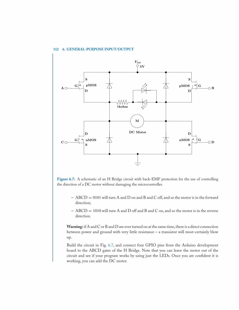
112 6. GENERAL-PURPOSE INPUT/OUTPUT
VDD
pMOS pMOS
M
nMOSnMOS
G
D
S
B
D
S
GG
G
D
S
S
D
D
A
C
DC Motor
5V
1kohm
Figure 6.7: A schematic of an H Bridge circuit with back-EMF protection for the use of controllingthe direction of a DC motor without damaging the microcontroller.
– ABCD = 0101 will turn A and D on and B and C off, and so the motor is in the forwarddirection;
– ABCD = 1010 will turn A and D off and B and C on, and so the motor is in the reversedirection.
Warning: if A and C or B and D are ever turned on at the same time, there is a direct connectionbetween power and ground with very little resistance – a transistor will most-certainly blowup.
Build the circuit in Fig. 6.7, and connect four GPIO pins from the Arduino developmentboard to the ABCD gates of the H Bridge. Note that you can leave the motor out of thecircuit and see if your program works by using just the LEDs. Once you are confident it isworking, you can add the DC motor.

6.4. PERTINENT REGISTER DESCRIPTIONS 113
6.6 Referring to problem 6.5, write a function that will turn on the motor in both directions, orturn off the motor based on an input variable.
6.7 Write a program that monitors and debounces an input switch. When the user presses theswitch, turn on a DC motor in the forward direction. When the user presses the switch asecond time, turn off the motor. You are welcome to modify this step in more interesting ways,but the user should be able to turn on and off the motor via the input push-button switch.


115
C H A P T E R 7
Timer Ports
7.1 PULSE WIDTH MODULATION
7.1.1 INTRODUCTIONSeveral modulation methods have been developed for applications that require a digital represen-tation of an analog signal. One popular and relevant scheme is pulse width modulation (PWM) inwhich the instantaneous amplitude of an analog signal is represented by the width of periodic squarewave. For example, consider the signals depicted in Fig. 7.1. Notice, the PWM version of the signalhas a fixed frequency defining the point when a pulse begins. During the period of an individualpulse, the signal remains high for an amount of time proportional to the amplitude of the analogsignal.
Vmax
Vmin
0
VCC
Figure 7.1: An example analog signal and a pulse width modulated representation.

116 7. TIMER PORTS
Recall the duty cycle of a square wave is given by
D = τ
T
where 0 ≤ τ ≤ T is the amount of time a signal is non-zero and T is the period of the square wave.Effectively, the pulse duty cycle represents a measure of the analog signal amplitude. Specifically,when the amplitude of a signal is at or below some minimal voltage Vmin, the PWM pulses have a0% duty cycle. Similarly, when a signal is at or above some maximal voltage Vmax , the PWM pulseshave a 100% duty cycle. Ideally, when the amplitude of a signal is in between Vmin and Vmax , theduty cycle of the PWM pulses is defined by the linear relation
D = Vsig − Vmin
Vmax − Vmin
where Vsig is the analog signal.
7.1.2 DEMODULATIONConverting the square-wave signal to the desired analog value is referred to as demodulation, andrequires a demodulator circuit to use the pulse widths as a measure for the signal amplitude. Considerthe simple low-pass filter (LPF) shown in Fig. 7.2. Recall, the -3 dB (or high-cutoff ) frequency is
vi(t)
R
C
vo(t)
Figure 7.2: A simple low-pass filter.
determined by the choice of R and C using the relation fh = 12πRC
. It is a well-known result that iffm � fh � ft , then an approximation of the original signal is recovered. Here, fm is the maximumfrequency of the analog message signal, and ft is the frequency of the PWM square-wave. Thus, thefilter needs to be designed such that the highest frequency of the desired analog signal is less thanfh.
In practice, most systems do not construct an explicit LPF before the load, which is typicallyeither inductive or capacitive. Instead, the natural frequency response of the load is used to demod-
7.1. PULSE WIDTH MODULATION 117
ulate the PWM pulses directly. In either case, effectively the voltage of the original message signalis delivered to the load via averaging over the PWM pulses.
7.1.3 MODULATIONThe remaining component to outputting an analog signal from a digital microcontroller is to generatethe appropriate PWM waveform, a process referred to as modulation; i.e, an analog message signalmodulates the square-wave carrier by altering its duty cycle. Most microcontrollers provide at leastone port that has timer sub-circuitry capable of generating PWM signals on a port pin. Typically,one just needs to configure the square-wave frequency and desired duty cycle via a couple of registers.When enabled, the port pin will output a PWM signal that can be demodulated in order to providean approximation to an analog signal.
In the case of the ATmega328P, there are two 8-bit timers and one 16-bit timer, all of whichare capable of generating PWM outputs. The registers are listed in Sec. 7.3.
Note, in the init() function within the Wiring library, all three timers are pre-initializedwith some specific functionality in mind. In particular, the often used delay() function relies on atimer 0 interrupt, and so we will avoid using it for the time being.
On the ATmega328P, three waveform generation bits exist within the two timer/countercontrol registers. Four of the eight possible waveform generation modes involve PWM waveformoutputs, two of which are considered fast PWM while the remaining two are called phase-correctPWM. Shown in Fig. 7.3 and Fig. 7.4 are the four different output waveforms given the specifiedwaveform configurations.
In general, the PWM generation circuitry operates based on the 8-bit or 16-bit count registerTCNT which updates its current value every time there is a clock pulse. As long as the TCNT valueis below the value stored in the output compare register OCRA or OCRB, then the associated outputpin OCA or OCB will remain in a specific state, for example, set high. Once the TCNT value becomesgreater than the compare register value, the output pin will switch to the opposite state, for exampleclear low. This operation will continue until the timer is disabled.
The first output mode shown in Fig. 7.3(a) represents the waveforms generated given a fastPWM setting where the TOP value is fixed at the maximum 8-bit value of 255. In this mode,two different output compare register values can be set independent of each other, each affecting adifferent output pin.That is, two separate PWM waveforms may be generated on two different portpins. Additionally, the period of the PWM waveform is T = 256/fclk , which is half the period ofthe phase-correct version, i.e., it is faster.
The second output mode shown in Fig. 7.3(b) represents the waveforms generated given thephase-correct PWM setting where the TOP value is also fixed at the maximum 8-bit value of 255.As in the fast PWM case, two different output compare register values can be set independent ofeach other, each affecting their own output pin. As can be seen, this mode alters the TCNT registerbehavior in that once the counter reaches the TOP value of 255, it begins counting backwardstoward 0. The benefit has to do with the phase of the modulated carrier. In particular, notice the

118 7. TIMER PORTS
t
TCNTx
t
OCxA
OCRxA
t
OCxB
OCRxB
T
255
0
0
5V
5V
0
t
TCNTx
t
OCxA
OCRxA
t
OCxB
OCRxB
T
255
0
0
5V
5V
0
(a) Fast PWM (b) Phase-Correct PWM
Figure 7.3: The two PWM configuration output waveforms with TOP = 255.
narrower pulses of OCB as compared to that of OCA in both Fig. 7.3(a-b). In the fast case, thefront edges line up, whereas in the phase-correct case, the center of the pulses line up; that is, thephase of the OCA and OCB waveforms are equivalent. As a result, the period of the PWM waveformis nearly doubled to T = (2 × 255)/fclk = 510/fclk , so less resolution is available. This is not atypo; in the fast PWM case, the counter follows the sequence {0, 1, ..., 254, 255, 0}, which impliesthere are 256 values in a single period. In the phase-correct case, the counter follows the sequence{0, 1, ..., 254, 255, 254, ..., 1, 0}, which implies there are (255 + 255) values in a single period.
The final two output modes shown in Fig. 7.4 represent the fast and phase-correct PWMwaveforms when the TOP value is set to the 8-bit value stored in OCRA. Both of these modes effec-tively disable the OCA pin functionality at the benefit of increasing the PWM frequency dramatically.In both cases, the TCNT register will count up to the OCRA value, and then either reset to 0 or startcounting down toward 0. The only comparison that matters is that to OCRB, which will affect theOCB pin as in the previous cases.The two most significant results are that for a value of N loaded intoOCRA, the total number of analog output levels available is reduced from 256 to N + 1. However,the periods of the two PWM waveforms are T = (N + 1)/fclk and T = (2N)/fclk , respectively.
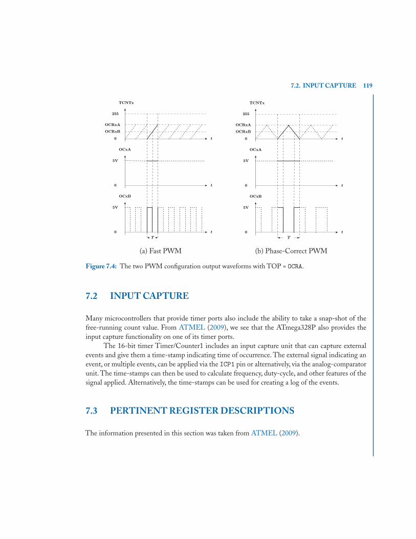
7.2. INPUT CAPTURE 119
t
TCNTx
t
OCxA
OCRxA
t
OCxB
OCRxB
T
255
0
0
5V
5V
0
t
TCNTx
t
OCxA
OCRxA
t
OCxB
OCRxB
T
255
0
0
5V
5V
0
(a) Fast PWM (b) Phase-Correct PWM
Figure 7.4: The two PWM configuration output waveforms with TOP = OCRA.
7.2 INPUT CAPTURE
Many microcontrollers that provide timer ports also include the ability to take a snap-shot of thefree-running count value. From ATMEL (2009), we see that the ATmega328P also provides theinput capture functionality on one of its timer ports.
The 16-bit timer Timer/Counter1 includes an input capture unit that can capture externalevents and give them a time-stamp indicating time of occurrence. The external signal indicating anevent, or multiple events, can be applied via the ICP1 pin or alternatively, via the analog-comparatorunit. The time-stamps can then be used to calculate frequency, duty-cycle, and other features of thesignal applied. Alternatively, the time-stamps can be used for creating a log of the events.
7.3 PERTINENT REGISTER DESCRIPTIONS
The information presented in this section was taken from ATMEL (2009).
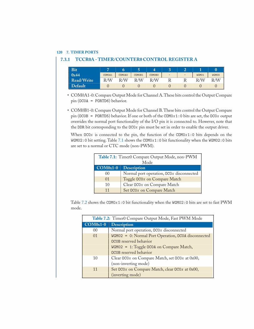
120 7. TIMER PORTS
7.3.1 TCCR0A - TIMER/COUNTER0 CONTROL REGISTER A
Bit 7 6 5 4 3 2 1 00x44 COM0A1 COM0A0 COM0B1 COM0B0 - - WGM01 WGM00
Read/Write R/W R/W R/W R/W R R R/W R/WDefault 0 0 0 0 0 0 0 0
• COM0A1-0: Compare Output Mode for Channel A.These bits control the Output Comparepin (OC0A = PORTD6) behavior.
• COM0B1-0: Compare Output Mode for Channel B.These bits control the Output Comparepin (OC0B = PORTD5) behavior. If one or both of the COM0x1:0 bits are set, the OC0x outputoverrides the normal port functionality of the I/O pin it is connected to. However, note thatthe DDR bit corresponding to the OC0x pin must be set in order to enable the output driver.
When OC0x is connected to the pin, the function of the COM0x1:0 bits depends on theWGM02:0 bit setting. Table 7.1 shows the COM0x1:0 bit functionality when the WGM02:0 bitsare set to a normal or CTC mode (non-PWM).
Table 7.1: Timer0 Compare Output Mode, non-PWMMode
COM0x1-0 Description00 Normal port operation, OC0x disconnected01 Toggle OC0x on Compare Match10 Clear OC0x on Compare Match11 Set OC0x on Compare Match
Table 7.2 shows the COM0x1:0 bit functionality when the WGM02:0 bits are set to fast PWMmode.
Table 7.2: Timer0 Compare Output Mode, Fast PWM ModeCOM0x1-0 Description
00 Normal port operation, OC0x disconnected01 WGM02 = 0: Normal Port Operation, OC0A disconnected
OC0B reserved behaviorWGM02 = 1: Toggle OC0A on Compare Match,OC0B reserved behavior
10 Clear OC0x on Compare Match, set OC0x at 0x00,(non-inverting mode)
11 Set OC0x on Compare Match, clear OC0x at 0x00,(inverting mode)

7.3. PERTINENT REGISTER DESCRIPTIONS 121
Table 7.3 shows the COM0x1:0 bit functionality when the WGM02:0 bits are set to phase correctPWM mode.
Table 7.3: Timer0 Compare Output Mode, Phase Correct PWM Mode
COM0x1-0 Description00 Normal port operation, OC0x disconnected01 WGM02 = 0: Normal Port Operation, OC0A disconnected
OC0B reserved behaviorWGM02 = 1: Toggle OC0A on Compare Match,OC0B reserved behavior
10 Clear OC0x on Compare Match when up-countingSet OC0x on Compare Match when down-counting
11 Set OC0x on Compare Match when up-countingClear OC0x on Compare Match when down-counting
• WGM01-0:Waveform Generation Mode.Combined with the WGM02 bit found in the TCCR0BRegister, these bits control the counting sequence of the counter, the source for maximum(TOP) counter value, and what type of waveform generation to be used, see Table 7.4. Modesof operation supported by the Timer/Counter unit are: Normal mode (counter), Clear Timeron Compare Match (CTC) mode, and two types of PWM modes.
Table 7.4: Timer0 Waveform Generation Mode Bit DescriptionOCR0x TOV0
WGM02-0 Mode TOP Update Flag Set000 Normal 0xFF Immediate 0xFF001 Phase Correct PWM 0xFF TOP 0x00010 CTC OCR0A Immediate 0xFF011 Fast PWM 0xFF 0x00 0xFF100 Reserved - - -101 Phase Correct PWM OCR0A TOP 0x00110 Reserved - - -111 Fast PWM OCR0A 0x00 TOP
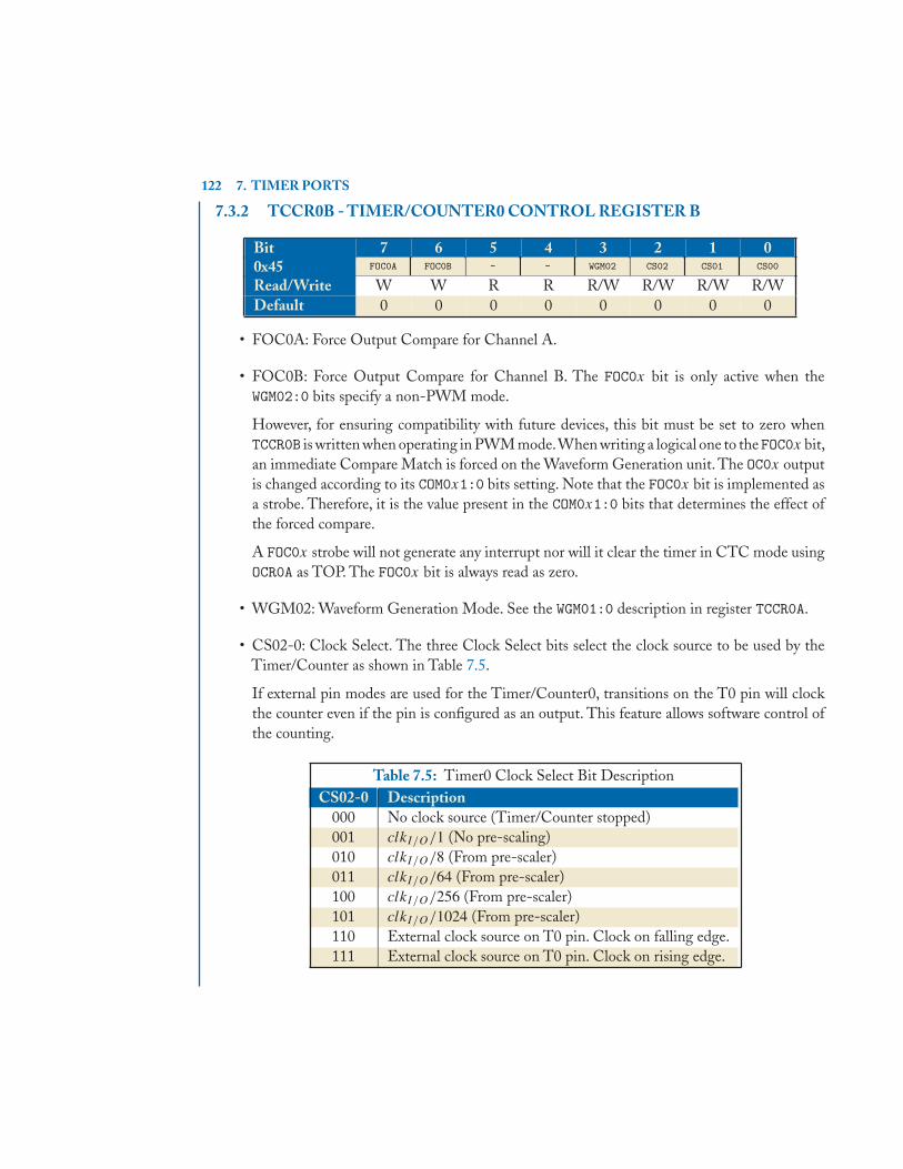
122 7. TIMER PORTS
7.3.2 TCCR0B - TIMER/COUNTER0 CONTROL REGISTER B
Bit 7 6 5 4 3 2 1 00x45 FOC0A FOC0B - - WGM02 CS02 CS01 CS00
Read/Write W W R R R/W R/W R/W R/WDefault 0 0 0 0 0 0 0 0
• FOC0A: Force Output Compare for Channel A.
• FOC0B: Force Output Compare for Channel B. The FOC0x bit is only active when theWGM02:0 bits specify a non-PWM mode.
However, for ensuring compatibility with future devices, this bit must be set to zero whenTCCR0B is written when operating in PWM mode.When writing a logical one to theFOC0x bit,an immediate Compare Match is forced on the Waveform Generation unit. The OC0x outputis changed according to its COM0x1:0 bits setting. Note that the FOC0x bit is implemented asa strobe. Therefore, it is the value present in the COM0x1:0 bits that determines the effect ofthe forced compare.
A FOC0x strobe will not generate any interrupt nor will it clear the timer in CTC mode usingOCR0A as TOP. The FOC0x bit is always read as zero.
• WGM02: Waveform Generation Mode. See the WGM01:0 description in register TCCR0A.
• CS02-0: Clock Select. The three Clock Select bits select the clock source to be used by theTimer/Counter as shown in Table 7.5.
If external pin modes are used for the Timer/Counter0, transitions on the T0 pin will clockthe counter even if the pin is configured as an output. This feature allows software control ofthe counting.
Table 7.5: Timer0 Clock Select Bit DescriptionCS02-0 Description
000 No clock source (Timer/Counter stopped)001 clkI/O/1 (No pre-scaling)010 clkI/O/8 (From pre-scaler)011 clkI/O/64 (From pre-scaler)100 clkI/O/256 (From pre-scaler)101 clkI/O/1024 (From pre-scaler)110 External clock source on T0 pin. Clock on falling edge.111 External clock source on T0 pin. Clock on rising edge.

7.3. PERTINENT REGISTER DESCRIPTIONS 123
7.3.3 TCNT0 - TIMER/COUNTER0 REGISTER
Bit 7 6 5 4 3 2 1 00x46 TCNT0[7:0]
Read/Write R/W R/W R/W R/W R/W R/W R/W R/WDefault 0 0 0 0 0 0 0 0
The Timer/Counter Register gives direct access, both for read and write operations, to theTimer/Counter unit 8-bit counter. Writing to the TCNT0 Register blocks (removes) the comparematch on the following timer clock for all compare units. Modifying TCNT0 while the counter isrunning, introduces a risk of missing a compare match between TCNT0 and the OCR0x Registers.
7.3.4 OCR0A - OUTPUT COMPARE0 REGISTER A
Bit 7 6 5 4 3 2 1 00x47 OCR0A[7:0]
Read/Write R/W R/W R/W R/W R/W R/W R/W R/WDefault 0 0 0 0 0 0 0 0
The Output Compare Register A contains an 8-bit value that is continuously compared withthe counter value TCNT0. A match can be used to generate an Output Compare interrupt or togenerate a waveform output on the OC0A = PORTD6 pin.
7.3.5 OCR0B - OUTPUT COMPARE0 REGISTER B
Bit 7 6 5 4 3 2 1 00x48 OCR0B[7:0]
Read/Write R/W R/W R/W R/W R/W R/W R/W R/WDefault 0 0 0 0 0 0 0 0
The Output Compare Register B contains an 8-bit value that is continuously compared withthe counter value TCNT0. A match can be used to generate an Output Compare interrupt or togenerate a waveform output on the OC0B = PORTD5 pin.
7.3.6 TCCR1A - TIMER/COUNTER1 CONTROL REGISTER A
Bit 7 6 5 4 3 2 1 00x80 COM1A1 COM1A0 COM1B1 COM1B0 - - WGM11 WGM10
Read/Write R/W R/W R/W R/W R R R/W R/WDefault 0 0 0 0 0 0 0 0
• COM1A1-0: Compare Output Mode for Channel A.These bits control the Output Comparepin (OC1A = PORTB1) behavior.

124 7. TIMER PORTS
• COM1B1-0: Compare Output Mode for Channel B.These bits control the Output Comparepin (OC1B = PORTB2) behavior. If one or both of the COM1x1:0 bits are set, the OC1x outputoverrides the normal port functionality of the I/O pin it is connected to. However, note thatthe DDR bit corresponding to the OC1x pin must be set in order to enable the output driver.
When OC1x is connected to the pin, the function of the COM1x1:0 bits depends on theWGM13:0 bit setting. Table 7.6 shows the COM1x1:0 bit functionality when the WGM13:0 bitsare set to a normal or CTC mode (non-PWM).
Table 7.6: Timer1 Compare Output Mode, non-PWMMode
COM1x1-0 Description00 Normal port operation, OC1x disconnected01 Toggle OC1x on Compare Match10 Clear OC1x on Compare Match11 Set OC1x on Compare Match
Table 7.7 shows the COM1x1:0 bit functionality when the WGM13:0 bits are set to fast PWMmode.
Table 7.7: Timer1 Compare Output Mode, Fast PWM ModeCOM1x1-0 Description
00 Normal port operation, OC1x disconnected01 WGM13:0 �= 14,15: Normal Port Operation, OC1x disconnected
WGM13:0 = 14,15: Toggle OC1A on Compare Match, OC1B disconnected10 Clear OC1x on Compare Match, set OC1x at 0x0000,
(non-inverting mode).11 Set OC1x on Compare Match, clear OC1x at 0x0000,
(inverting mode).
Table 7.8 shows the COM1x1:0 bit functionality when the WGM13:0 bits are set to phase correctPWM mode.
• WGM11-0: Waveform Generation Mode. Combined with the WGM13:2 bit found in theTCCR1B Register, these bits control the counting sequence of the counter, the source for max-imum (TOP) counter value, and what type of waveform generation to be used, see Table 7.9.Modes of operation supported by the Timer/Counter unit are: Normal mode (counter), ClearTimer on Compare Match (CTC) mode, and three types of PWM modes.

7.3. PERTINENT REGISTER DESCRIPTIONS 125
Table 7.8: Timer1 Compare Output Mode, Phase Correct PWM ModeCOM1x1-0 Description
00 Normal port operation, OC1x disconnected01 WGM13:0 �= 9,11: Normal Port Operation, OC1x disconnected
WGM13:0 = 9,11: Toggle OC1A on Compare Match, OC1B disconnected10 Clear OC1x on Compare Match when up-counting.
Set OC1x on Compare Match when down-counting.11 Set OC1x on Compare Match when up-counting.
Clear OC1x on Compare Match when down-counting.
Table 7.9: Timer1 Waveform Generation Mode Bit DescriptionOCR1x TOV1
WGM13-0 Mode TOP Update Flag Set0000 Normal 0xFFFF Immediate 0xFFFF0001 Phase Correct 8-bit PWM 0x00FF TOP 0x00000010 Phase Correct 9-bit PWM 0x01FF TOP 0x00000011 Phase Correct 10-bit PWM 0x03FF TOP 0x00000100 CTC OCR1A Immediate 0xFFFF0101 Fast 8-bit PWM 0x00FF 0x0000 TOP0110 Fast 9-bit PWM 0x01FF 0x0000 TOP0111 Fast 10-bit PWM 0x03FF 0x0000 TOP1000 Phase/Frequency Correct PWM ICR1 0x0000 0x00001001 Phase/Frequency Correct PWM OCR1A 0x0000 0x00001010 Phase Correct PWM ICR1 TOP 0x00001011 Phase Correct PWM OCR1A TOP 0x00001100 CTC ICR1 Immediate 0xFFFF1101 Reserved - - -1110 Fast PWM ICR1 0x0000 TOP1111 Fast PWM OCR1A 0x0000 TOP
7.3.7 TCCR1B - TIMER/COUNTER1 CONTROL REGISTER B
Bit 7 6 5 4 3 2 1 00x81 ICNC1 ICES1 - WGM13 WGM12 CS12 CS11 CS10
Read/Write R/W R/W R R/W R/W R/W R/W R/WDefault 0 0 0 0 0 0 0 0
• ICNC1: Input Capture Noise Canceler. Setting this bit (to one) activates the Input CaptureNoise Canceler. When the noise canceler is activated, the input from the Input Capture pin
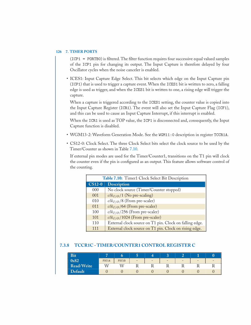
126 7. TIMER PORTS
(ICP1 = PORTB0) is filtered. The filter function requires four successive equal valued samplesof the ICP1 pin for changing its output. The Input Capture is therefore delayed by fourOscillator cycles when the noise canceler is enabled.
• ICES1: Input Capture Edge Select. This bit selects which edge on the Input Capture pin(ICP1) that is used to trigger a capture event. When the ICES1 bit is written to zero, a fallingedge is used as trigger, and when the ICES1 bit is written to one, a rising edge will trigger thecapture.
When a capture is triggered according to the ICES1 setting, the counter value is copied intothe Input Capture Register (ICR1). The event will also set the Input Capture Flag (ICF1),and this can be used to cause an Input Capture Interrupt, if this interrupt is enabled.
When the ICR1 is used as TOP value, the ICP1 is disconnected and, consequently, the InputCapture function is disabled.
• WGM13-2: Waveform Generation Mode. See the WGM11:0 description in register TCCR1A.
• CS12-0: Clock Select. The three Clock Select bits select the clock source to be used by theTimer/Counter as shown in Table 7.10.
If external pin modes are used for the Timer/Counter1, transitions on the T1 pin will clockthe counter even if the pin is configured as an output. This feature allows software control ofthe counting.
Table 7.10: Timer1 Clock Select Bit DescriptionCS12-0 Description
000 No clock source (Timer/Counter stopped)001 clkI/O/1 (No pre-scaling)010 clkI/O/8 (From pre-scaler)011 clkI/O/64 (From pre-scaler)100 clkI/O/256 (From pre-scaler)101 clkI/O/1024 (From pre-scaler)110 External clock source on T1 pin. Clock on falling edge.111 External clock source on T1 pin. Clock on rising edge.
7.3.8 TCCR1C - TIMER/COUNTER1 CONTROL REGISTER C
Bit 7 6 5 4 3 2 1 00x82 FOC1A FOC1B - - - - - -
Read/Write W W R R R R R RDefault 0 0 0 0 0 0 0 0

7.3. PERTINENT REGISTER DESCRIPTIONS 127
• FOC1A: Force Output Compare for Channel A.
• FOC1B: Force Output Compare for Channel B. The FOC1x bit is only active when theWGM13:0 bits specify a non-PWM mode. When writing a logical one to the FOC1x bit, animmediate Compare Match is forced on the Waveform Generation unit. The OC1x output ischanged according to its COM1x1:0 bits setting. Note that the FOC1x bit is implemented asa strobe. Therefore, it is the value present in the COM1x1:0 bits that determines the effect ofthe forced compare.
A FOC1x strobe will not generate any interrupt, nor will it clear the timer in CTC mode usingOCR1A as TOP. The FOC1x bit is always read as zero.
7.3.9 TCNT1H AND TCNT1L - TIMER/COUNTER1 REGISTER
Bit 7 6 5 4 3 2 1 00x85 TCNT1[15:8]
0x84 TCNT1[7:0]
Read/Write R/W R/W R/W R/W R/W R/W R/W R/WDefault 0 0 0 0 0 0 0 0
The two Timer/Counter Registers give direct access, both for read and write operations, tothe Timer/Counter unit 16-bit counter. To ensure that both the high and low bytes are read andwritten simultaneously when the CPU accesses these registers, the access is performed using an 8-bittemporary High Byte Register (TEMP). This temporary register is shared by all the other 16-bitregisters.
Writing to the TCNT1 Register blocks (removes) the compare match on the following timerclock for all compare units. Modifying TCNT1 while the counter is running, introduces a risk ofmissing a Compare Match between TCNT1 and the OCR1x Registers.
7.3.10 OCR1AH AND OCR1AL - OUTPUT COMPARE1 REGISTER A
Bit 7 6 5 4 3 2 1 00x89 OCR1A[15:8]
0x88 OCR1A[7:0]
Read/Write R/W R/W R/W R/W R/W R/W R/W R/WDefault 0 0 0 0 0 0 0 0
The Output Compare Register A contains a 16-bit value that is continuously compared withthe counter value TCNT1. A match can be used to generate an Output Compare interrupt or togenerate a waveform output on the OC1A = PORTB1 pin.
The Output Compare Registers are 16-bit in size. To ensure that both the high and low bytesare written simultaneously when the CPU writes to these registers, the access is performed using

128 7. TIMER PORTS
an 8-bit temporary High Byte Register (TEMP). This temporary register is shared by all the other16-bit registers.
7.3.11 OCR1BH AND OCR1BL - OUTPUT COMPARE1 REGISTER B
Bit 7 6 5 4 3 2 1 00x8B OCR1B[15:8]
0x8A OCR1B[7:0]
Read/Write R/W R/W R/W R/W R/W R/W R/W R/WDefault 0 0 0 0 0 0 0 0
The Output Compare Register B contains a 16-bit value that is continuously compared withthe counter value TCNT1. A match can be used to generate an Output Compare interrupt or togenerate a waveform output on the OC1B = PORTB2 pin.
The Output Compare Registers are 16-bit in size. To ensure that both the high and low bytesare written simultaneously when the CPU writes to these registers, the access is performed usingan 8-bit temporary High Byte Register (TEMP). This temporary register is shared by all the other16-bit registers.
7.3.12 ICR1H AND ICR1L - INPUT CAPTURE1 REGISTER
Bit 7 6 5 4 3 2 1 00x87 ICR1[15:8]
0x86 ICR1[7:0]
Read/Write R/W R/W R/W R/W R/W R/W R/W R/WDefault 0 0 0 0 0 0 0 0
The Input Capture is updated with the counter TCNT1 value each time an event occurs on theICP1 = PORTB0 pin (or optionally on the Analog Comparator output for Timer/Counter1). TheInput Capture can be used for defining the counter TOP value.
The Output Compare Registers are 16-bit in size. To ensure that both the high and low bytesare written simultaneously when the CPU writes to these registers, the access is performed usingan 8-bit temporary High Byte Register (TEMP). This temporary register is shared by all the other16-bit registers.
7.3.13 TCCR2A - TIMER/COUNTER2 CONTROL REGISTER A
Bit 7 6 5 4 3 2 1 00xB0 COM2A1 COM2A0 COM2B1 COM2B0 - - WGM21 WGM20
Read/Write R/W R/W R/W R/W R R R/W R/WDefault 0 0 0 0 0 0 0 0

7.3. PERTINENT REGISTER DESCRIPTIONS 129
• COM2A1-0: Compare Output Mode for Channel A.These bits control the Output Comparepin (OC2A = PORTB3) behavior.
• COM2B1-0: Compare Output Mode for Channel B.These bits control the Output Comparepin (OC2B = PORTD3) behavior. If one or both of the COM2x1:0 bits are set, the OC2x outputoverrides the normal port functionality of the I/O pin it is connected to. However, note thatthe DDR bit corresponding to the OC2x pin must be set in order to enable the output driver.
When OC2x is connected to the pin, the function of the COM2x1:0 bits depends on theWGM22:0 bit setting.Table 7.11 shows the COM2x1:0 bit functionality when the WGM22:0 bitsare set to a normal or CTC mode (non-PWM).
Table 7.11: Timer2 Compare Output Mode, non-PWMModeCOM2x1-0 Description
00 Normal port operation, OC2x disconnected01 Toggle OC2x on Compare Match10 Clear OC2x on Compare Match11 Set OC2x on Compare Match
Table 7.12 shows the COM2x1:0 bit functionality when the WGM22:0 bits are set to fast PWMmode.
Table 7.12: Timer2 Compare Output Mode, Fast PWM ModeCOM2x1-0 Description
00 Normal port operation, OC2x disconnected01 WGM22 = 0: Normal Port Operation, OC2A disconnected
OC2B reserved behaviorWGM22 = 1: Toggle OC2A on Compare Match,OC2B reserved behavior
10 Clear OC2x on Compare Match, set OC2x at 0x00,(non-inverting mode).
11 Set OC2x on Compare Match, clear OC2x at 0x00,(inverting mode).
Table 7.13 shows the COM2x1:0 bit functionality when the WGM22:0 bits are set to phasecorrect PWM mode.
• WGM21-0:Waveform Generation Mode.Combined with the WGM22 bit found in the TCCR2BRegister, these bits control the counting sequence of the counter, the source for maximum(TOP) counter value, and what type of waveform generation to be used, see Table 7.14.
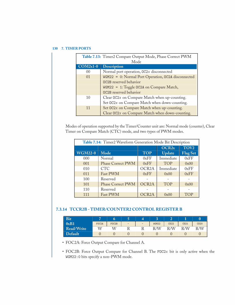
130 7. TIMER PORTS
Table 7.13: Timer2 Compare Output Mode, Phase Correct PWMMode
COM2x1-0 Description00 Normal port operation, OC2x disconnected01 WGM22 = 0: Normal Port Operation, OC2A disconnected
OC2B reserved behaviorWGM22 = 1: Toggle OC2A on Compare Match,OC2B reserved behavior
10 Clear OC2x on Compare Match when up-counting.Set OC2x on Compare Match when down-counting.
11 Set OC2x on Compare Match when up-counting.Clear OC2x on Compare Match when down-counting.
Modes of operation supported by the Timer/Counter unit are: Normal mode (counter), ClearTimer on Compare Match (CTC) mode, and two types of PWM modes.
Table 7.14: Timer2 Waveform Generation Mode Bit DescriptionOCR2x TOV2
WGM22-0 Mode TOP Update Flag Set000 Normal 0xFF Immediate 0xFF001 Phase Correct PWM 0xFF TOP 0x00010 CTC OCR2A Immediate 0xFF011 Fast PWM 0xFF 0x00 0xFF100 Reserved - - -101 Phase Correct PWM OCR2A TOP 0x00110 Reserved - - -111 Fast PWM OCR2A 0x00 TOP
7.3.14 TCCR2B - TIMER/COUNTER2 CONTROL REGISTER B
Bit 7 6 5 4 3 2 1 00xB1 FOC2A FOC2B - - WGM22 CS22 CS21 CS20
Read/Write W W R R R/W R/W R/W R/WDefault 0 0 0 0 0 0 0 0
• FOC2A: Force Output Compare for Channel A.
• FOC2B: Force Output Compare for Channel B. The FOC2x bit is only active when theWGM22:0 bits specify a non-PWM mode.
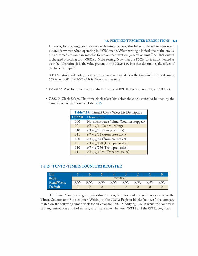
7.3. PERTINENT REGISTER DESCRIPTIONS 131
However, for ensuring compatibility with future devices, this bit must be set to zero whenTCCR2B is written when operating in PWM mode. When writing a logical one to the FOC2xbit, an immediate compare match is forced on the waveform generation unit.The OC2x outputis changed according to its COM2x1:0 bits setting. Note that the FOC2x bit is implemented asa strobe. Therefore, it is the value present in the COM2x1:0 bits that determines the effect ofthe forced compare.
A FOC2x strobe will not generate any interrupt, nor will it clear the timer in CTC mode usingOCR2A as TOP. The FOC2x bit is always read as zero.
• WGM22: Waveform Generation Mode. See the WGM21:0 description in register TCCR2A.
• CS22-0: Clock Select. The three clock select bits select the clock source to be used by theTimer/Counter as shown in Table 7.15.
Table 7.15: Timer2 Clock Select Bit DescriptionCS22-0 Description
000 No clock source (Timer/Counter stopped)001 clkT 2S/1 (No pre-scaling)010 clkT 2S/8 (From pre-scaler)011 clkT 2S/32 (From pre-scaler)100 clkT 2S/64 (From pre-scaler)101 clkT 2S/128 (From pre-scaler)110 clkT 2S/256 (From pre-scaler)111 clkT 2S/1024 (From pre-scaler)
7.3.15 TCNT2 - TIMER/COUNTER2 REGISTER
Bit 7 6 5 4 3 2 1 00xB2 TCNT2[7:0]
Read/Write R/W R/W R/W R/W R/W R/W R/W R/WDefault 0 0 0 0 0 0 0 0
The Timer/Counter Register gives direct access, both for read and write operations, to theTimer/Counter unit 8-bit counter. Writing to the TCNT2 Register blocks (removes) the comparematch on the following timer clock for all compare units. Modifying TCNT2 while the counter isrunning, introduces a risk of missing a compare match between TCNT2 and the OCR2x Registers.
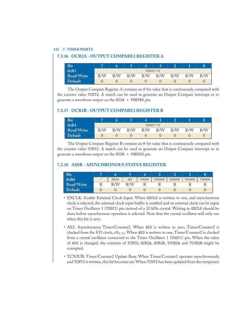
132 7. TIMER PORTS
7.3.16 OCR2A - OUTPUT COMPARE2 REGISTER A
Bit 7 6 5 4 3 2 1 00xB3 OCR2A[7:0]
Read/Write R/W R/W R/W R/W R/W R/W R/W R/WDefault 0 0 0 0 0 0 0 0
The Output Compare Register A contains an 8-bit value that is continuously compared withthe counter value TCNT2. A match can be used to generate an Output Compare interrupt or togenerate a waveform output on the OC2A = PORTB3 pin.
7.3.17 OCR2B - OUTPUT COMPARE2 REGISTER B
Bit 7 6 5 4 3 2 1 00xB4 OCR2B[7:0]
Read/Write R/W R/W R/W R/W R/W R/W R/W R/WDefault 0 0 0 0 0 0 0 0
The Output Compare Register B contains an 8-bit value that is continuously compared withthe counter value TCNT2. A match can be used to generate an Output Compare interrupt or togenerate a waveform output on the OC2B = PORTD3 pin.
7.3.18 ASSR - ASYNCHRONOUS STATUS REGISTER
Bit 7 6 5 4 3 2 1 00xB6 - EXCLK AS2 TCN2UB OCR2AUB OCR2BUB TCR2AUB TCR2BUB
Read/Write R R/W R/W R R R R RDefault 0 0 0 0 0 0 0 0
• EXCLK: Enable External Clock Input. When EXCLK is written to one, and asynchronousclock is selected, the external clock input buffer is enabled and an external clock can be inputon Timer Oscillator 1 (TOSC1) pin instead of a 32 kHz crystal. Writing to EXCLK should bedone before asynchronous operation is selected. Note that the crystal oscillator will only runwhen this bit is zero.
• AS2: Asynchronous Timer/Counter2. When AS2 is written to zero, Timer/Counter2 isclocked from the I/O clock, clkI/O . When AS2 is written to one, Timer/Counter2 is clockedfrom a crystal oscillator connected to the Timer Oscillator 1 (TOSC1) pin. When the valueof AS2 is changed, the contents of TCNT2, OCR2A, OCR2B, TCCR2A and TCCR2B might becorrupted.
• TCN2UB: Timer/Counter2 Update Busy. When Timer/Counter2 operates asynchronouslyand TCNT2 is written, this bit becomes set. When TCNT2 has been updated from the temporary
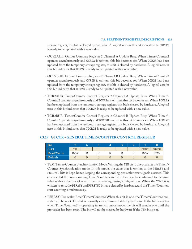
7.3. PERTINENT REGISTER DESCRIPTIONS 133
storage register, this bit is cleared by hardware. A logical zero in this bit indicates that TCNT2is ready to be updated with a new value.
• OCR2AUB: Output Compare Register 2 Channel A Update Busy. When Timer/Counter2operates asynchronously and OCR2A is written, this bit becomes set. When OCR2A has beenupdated from the temporary storage register, this bit is cleared by hardware. A logical zero inthis bit indicates that OCR2A is ready to be updated with a new value.
• OCR2BUB: Output Compare Register 2 Channel B Update Busy. When Timer/Counter2operates asynchronously and OCR2B is written, this bit becomes set. When OCR2B has beenupdated from the temporary storage register, this bit is cleared by hardware. A logical zero inthis bit indicates that OCR2B is ready to be updated with a new value.
• TCR2AUB: Timer/Counter Control Register 2 Channel A Update Busy. When Timer/-Counter2 operates asynchronously and TCCR2A is written, this bit becomes set. When TCCR2Ahas been updated from the temporary storage register, this bit is cleared by hardware. A logicalzero in this bit indicates that TCCR2A is ready to be updated with a new value.
• TCR2BUB: Timer/Counter Control Register 2 Channel B Update Busy. When Timer/-Counter2 operates asynchronously and TCCR2B is written, this bit becomes set. When TCCR2Bhas been updated from the temporary storage register, this bit is cleared by hardware. A logicalzero in this bit indicates that TCCR2B is ready to be updated with a new value.
7.3.19 GTCCR - GENERAL TIMER/COUNTER CONTROL REGISTER
Bit 7 6 5 4 3 2 1 00x43 TSM - - - - - PSRASY PSRSYNC
Read/Write R/W R R R R R R/W R/WDefault 0 0 0 0 0 0 0 0
• TSM:Timer/Counter Synchronization Mode.Writing theTSMbit to one activates theTimer/-Counter Synchronization mode. In this mode, the value that is written to the PSRASY andPSRSYNC bits is kept, hence keeping the corresponding pre-scaler reset signals asserted. Thisensures that the corresponding Timer/Counters are halted and can be configured to the samevalue without the risk of one of them advancing during configuration. When the TSM bit iswritten to zero, thePSRASY andPSRSYNC bits are cleared by hardware, and theTimer/Countersstart counting simultaneously.
• PSRASY: Pre-scaler Reset Timer/Counter2 When this bit is one, the Timer/Counter2 pre-scaler will be reset. This bit is normally cleared immediately by hardware. If the bit is writtenwhen Timer/Counter2 is operating in asynchronous mode, the bit will remain one until thepre-scaler has been reset. The bit will not be cleared by hardware if the TSM bit is set.

134 7. TIMER PORTS
• PSRSYNC: Pre-scaler Reset When this bit is one, Timer/Counter1 and Timer/Counter0pre-scaler will be reset. This bit is normally cleared immediately by hardware, except if theTSM bit is set. Note that Timer/Counter1 and Timer/Counter0 share the same pre-scaler anda reset of this pre-scaler will affect both timers.
PROBLEMS7.1 Determine the appropriate bit settings for TCCR2A and TCCR2B to generate a PWM output
using the following specific details
– use channel B for the output waveform,
– use phase-correct PWM mode,
– use clear on up-counting, set on down-counting,
– have TOP defined as OCR2A,
– use a pre-scaler division value of 1.
7.2 Create a function that initializes timer 2 based on the values determined in problem 7.1.Additionally, set the OCR2A value to something that allows for a small-enough period suchthat the resulting analog output (after LPF) has a small amount of ripple. Note this last stepwill involve trial-and-error; a small value will allow a higher PWM frequency which will resultin less ripple, but there will be fewer possible output levels; a large value will result in moreripple in an output signal.
7.3 Create a function that takes as an input a floating point number between 0 and 1. Based onthe floating point value, the function needs to set the appropriate percent value in the OCR2Bregister. For example, if the input value is 0.6, then the count should be 60% of TOP.
7.4 Write a program that outputs a 2 kHz, 0 to 5 V saw-tooth PWM signal. Have the port pinoutput to a simple LPF where the fh is well above 2 kHz (e.g., 16 kHz). Use an oscilloscopeto verify your signal. Note that DDRx still has to be set to an output for the PWM port pin.
Tip: in order to generate a 2 kHz signal, you will have to repeatedly call the function you createdin problem 7.3 with the appropriate analog value between 0 and 1, and with the appropriateamount of delay between samples. The delay() function is too slow to allow for a 2 kHzsignal, but you can use either micros() to see how much time has passed from a previous call(like polling an input switch), or delayMicroseconds() to force a specific delay.
7.5 Write a program that monitors and debounces an input switch. As the user presses the switch,generate a 2 kHz sinusoid, a 2 kHz triangle wave, and a 2 kHz saw-tooth wave. Another pressshould turn off the output all together.

135
C H A P T E R 8
Analog Input Ports
8.1 ANALOG-TO-DIGITAL CONVERTERSAn important aspect to most embedded systems involves one or more input signals. Up until now,any input messages that you have seen in previous chapters have been strictly digital. However,most naturally occurring signals are analog, meaning the voltage level can be any value within someinterval Vmin ≤ VA ≤ Vmax . In many systems, different actions and decisions are made based on thevalue of VA. For example, consider the following list of analog sensor devices.
• Potentiometer - a mechanical knob is used to adjust the resistance between terminals;
• Thermistor - a device that changes resistance based on temperature;
• Accelerometer - a device that measures the acceleration of gravity in three dimensions and out-puts an associated analog value for each dimension (e.g., this is the basis behind the NintendoWii video-game controllers);
• Ambient light sensor - a device that measure the environmental ambient light intensity andoutputs an associated analog value (e.g., many laptop computers will adjust the backlight levelbased on the surrounding environment light level);
• Microphone - a device that converts vibrations (i.e., acoustic-waves) into analog levels.
This is only a small list of many devices that are necessary for bridging the analog environment inwhich we live to the digital world in which we perform computations. However, these device onlyprovide the analog voltages and currents. In order for a microcontroller to operate on the sensoroutputs, an Analog-to-Digital Conversion (ADC) circuit must be used, such as depicted in Fig. 8.1.
The parallel ADC shown in Fig. 8.1 uses typical values for Vmin and Vmax where the minimumvoltage is simply set to ground and Vmax is controlled externally via the user-defined reference voltageVREF . The resistor network on the left-hand side is designed such that
VREF − V2 = V2 − V1 = V1 − V0 = V0
which implies there is uniform spacing between the inverting inputs on all of the comparators. Theanalog voltage VA is first converted into a three-bit codeword defined by (c2c1c0), where each bit isthe output of a comparator.This can be seen in Fig. 8.2, where VA is swept from 0 to VREF .The four
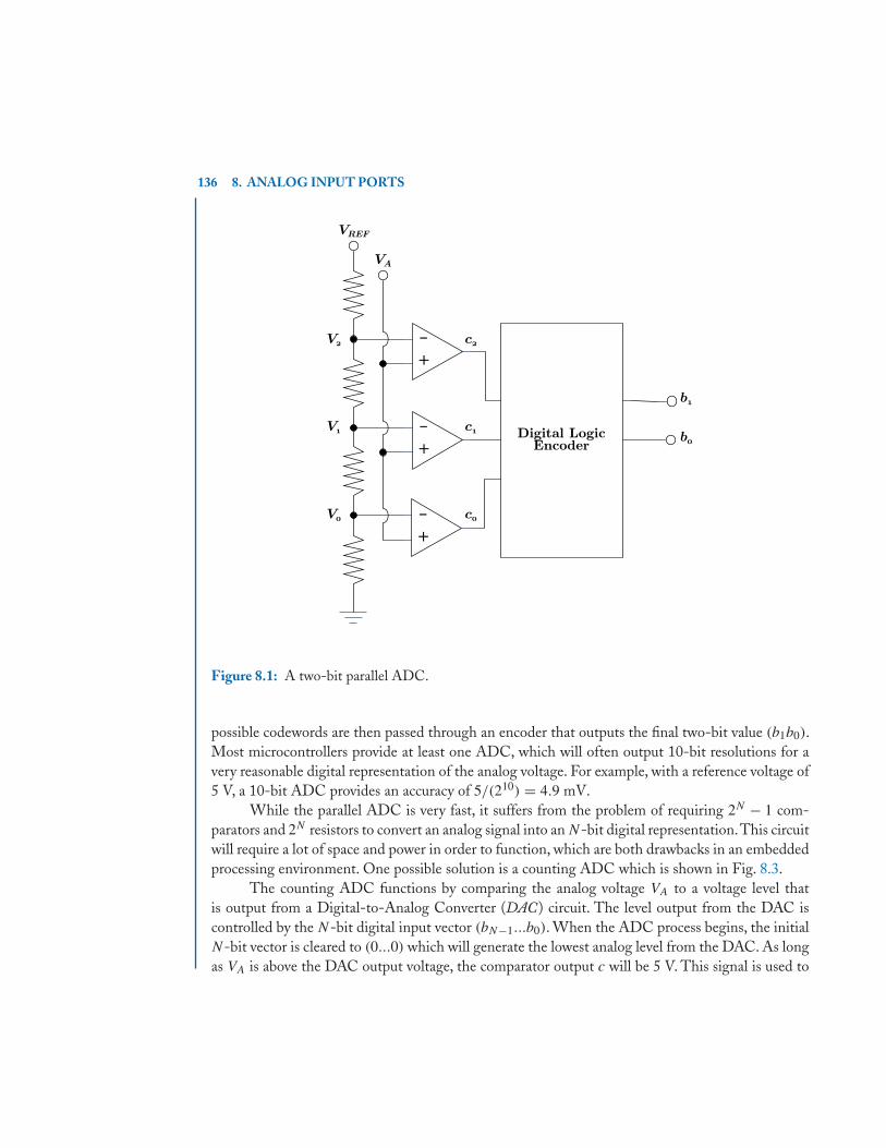
136 8. ANALOG INPUT PORTS
-+
-+
-+
VREF
VA
Digital LogicEncoder
c0
c1
c2
b0
b1
V2
V1
V0
Figure 8.1: A two-bit parallel ADC.
possible codewords are then passed through an encoder that outputs the final two-bit value (b1b0).Most microcontrollers provide at least one ADC, which will often output 10-bit resolutions for avery reasonable digital representation of the analog voltage. For example, with a reference voltage of5 V, a 10-bit ADC provides an accuracy of 5/(210) = 4.9 mV.
While the parallel ADC is very fast, it suffers from the problem of requiring 2N − 1 com-parators and 2N resistors to convert an analog signal into an N-bit digital representation.This circuitwill require a lot of space and power in order to function, which are both drawbacks in an embeddedprocessing environment. One possible solution is a counting ADC which is shown in Fig. 8.3.
The counting ADC functions by comparing the analog voltage VA to a voltage level thatis output from a Digital-to-Analog Converter (DAC) circuit. The level output from the DAC iscontrolled by the N-bit digital input vector (bN−1...b0). When the ADC process begins, the initialN-bit vector is cleared to (0...0) which will generate the lowest analog level from the DAC. As longas VA is above the DAC output voltage, the comparator output c will be 5 V. This signal is used to

8.1. ANALOG-TO-DIGITAL CONVERTERS 137
t
Comparisons
0
VA
V2V1V0
VREF
t0
5V
c2
t0
5V
c1
t0
5V
c0
Figure 8.2: The initial ADC codewords defined by the output of individual comparators.
enable the counter to increase the N-bit vector by one when the next clock edge occurs. Eventually,the N-bit vector will increase to the point that the DAC output voltage is greater than VA, at whichtime, c will go to 0, which will stop the counter. In this way, the N-bit value used to control theDAC output voltage is also the same value that represents VA. The drawback of the counting ADCis the time necessary for the counter to lock onto the proper binary output vector. It is often the casethat ADCs found in embedded processors do require some significant delay before the digital valuecan be trusted.
For the sake of completeness, and for anyone who might be curious, an N-bit DAC circuitmay be realized as in Fig. 8.4. This particular topology is nice because only two different resistorvalues are used, R for all horizontally-drawn resistors and 2R for all vertically-drawn resistors. TheR-2R ladder is designed so that the amount of current entering each switch is a factor of two lessthan that of the switch immediately proceeding it.Then each bi will control if that particular amountof current is passed to the feedback path or not. The result is 2N different combinations of current

138 8. ANALOG INPUT PORTS
D/A Converter
Counter-+VA
Clk
b0
b1
bN-1
c
VREF
Figure 8.3: An N-bit counting ADC.
-+
bN-1b1b0
VREF
VA
Figure 8.4: An N-bit R-2R ladder network DAC.
being sent to the feedback resistor, which provides 2N different output voltages uniformly separatedbetween 0 and −VREF . So, there needs to be some additional circuitry (not shown) in order to invertthe voltage so VA is between 0 and VREF .
8.1.1 ADC PERIPHERALIn the case of the ATmega328P, there are six 10-bit ADCs (note: there are eight 10-bit ADCs onsome packages, but not on the package present on the Arduino development board), all of whichare found on Port C. The registers are listed in Sec. 8.3.
Note, in the init() function within the Wiring library, the ADC peripheral system is pre-initialized only so far as to set the pre-scalar and turn on the ADC functionality.
For generic usage of the ADC port functionality, the following steps should be addressed.
• Register ADCSRA needs to be enabled, started, auto trigger enabled, and an appropriate pre-scalar selected;

8.1. ANALOG-TO-DIGITAL CONVERTERS 139
• register ADCSRB needs to have the auto trigger source set to free running, so the program canread the converted value of a low-frequency sensor (which is often our application);
• register ADMUX needs to have a VREF source selected, right or left justification selected, andthe desired ADC channel selected;
• register DIDR0 should have the input pin associated with the ADC channel selected in ADMUXdisabled.
Once the ADC is initialized, the program can poll the ADC output by reading the 16-bit ADCregister which contains the 10-bit result. As the math implies, eight bits sit in one 8-bit register andthe remaining two bits are provided in the other register, with six bits being unused. It turns out thatthe ADC hardware will not update the ADC register until the ADCH portion is read out by itself, orthe entire 16-bit register is read out as a single unit. So, if only eight bits of resolution are needed, theADC value can be left-justified in ADMUX and the high-order byte may be read, as in the followingcode snip.
Example 8.1
unsignedunsignedunsigned charcharchar *portADCDataRegisterHigh;unsignedunsignedunsigned charcharchar value;
portADCDataRegisterHigh = (unsignedunsignedunsigned charcharchar *) 0x79;
value = *portADCDataRegisterHigh;
However, if all 10 bits of resolution are necessary, then the two registers comprising the 16-bit spaceneed to be accessed as in the following code snip (assuming left justification in ADMUX).
Example 8.2
unsignedunsignedunsigned shortshortshort *portADCDataRegister;unsignedunsignedunsigned shortshortshort value;
portADCDataRegister = (unsignedunsignedunsigned shortshortshort *) 0x78;
value = (* portADCDataRegister & 0xFFC0) >> 6;
Or, if right justification is used, the following would be more appropriate.
140 8. ANALOG INPUT PORTS
Example 8.3
unsignedunsignedunsigned shortshortshort *portADCDataRegister;unsignedunsignedunsigned shortshortshort value;
portADCDataRegister = (unsignedunsignedunsigned shortshortshort *) 0x78;
value = (* portADCDataRegister & 0x03FF);
8.2 ANALOG COMPARATORIn addition to the ADC peripheral, the ATmega328P also provides a pure analog comparator pe-ripheral. As shown in the simplified schematic in Fig. 8.5, two external input pins are connected tothe two inputs of an op-amp configured as a comparator. As a result, software can use this periph-eral in order to constantly monitor two analog signals. When the voltage on the positive terminalbecomes greater than that of the negative terminal, the output signal is set. The comparator’s outputsignal can be used to trigger the Timer1 input capture function, or else it can be used to generate anindependent interrupt signal.
-+
AIN1
AIN0
ACO
Figure 8.5: Simplified schematic of the analog comparator peripheral.
8.3 PERTINENT REGISTER DESCRIPTIONSThe information presented in this section was taken from ATMEL (2009).
8.3.1 ADMUX - ADC MULTIPLEXER SELECTION REGISTER
Bit 7 6 5 4 3 2 1 00x7C REFS1 REFS0 ADLAR - MUX3 MUX2 MUX1 MUX0
Read/Write R/W R/W R/W R R/W R/W R/W R/WDefault 0 0 0 0 0 0 0 0
• REFS1-0: Reference Selection Bits. These bits select the voltage reference for the ADC, asshown in Table 8.1. If these bits are changed during a conversion, the change will not go in
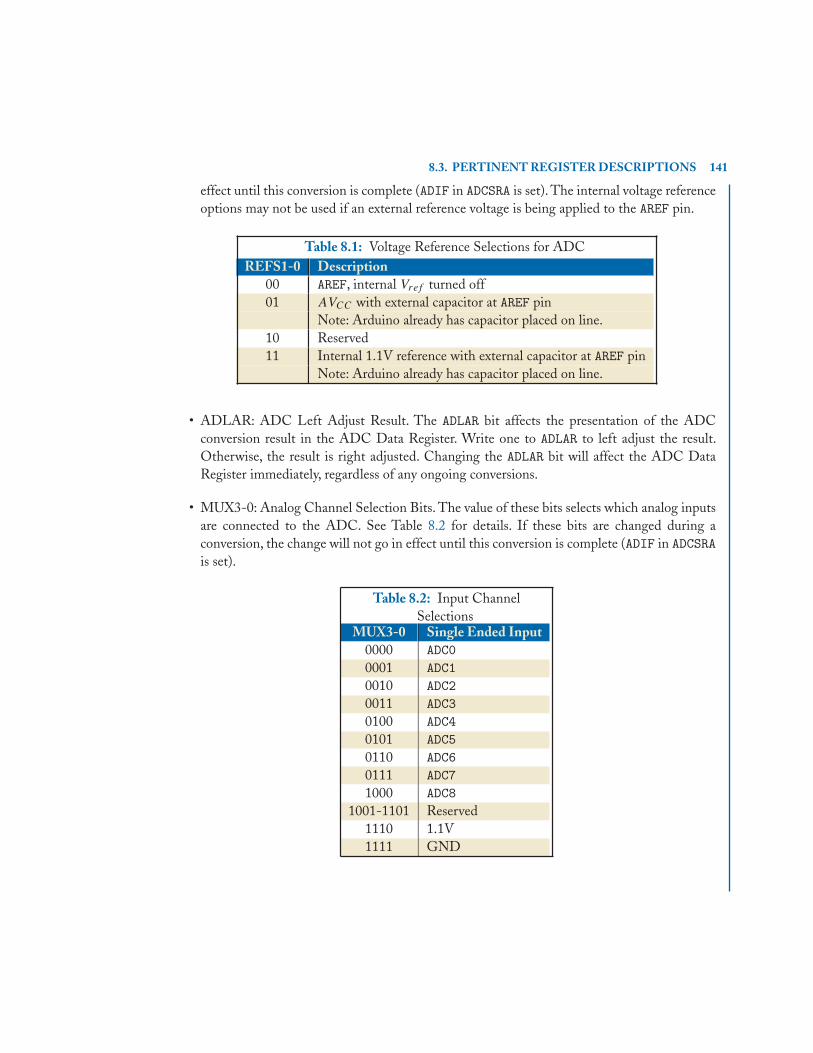
8.3. PERTINENT REGISTER DESCRIPTIONS 141
effect until this conversion is complete (ADIF in ADCSRA is set). The internal voltage referenceoptions may not be used if an external reference voltage is being applied to the AREF pin.
Table 8.1: Voltage Reference Selections for ADCREFS1-0 Description
00 AREF, internal Vref turned off01 AVCC with external capacitor at AREF pin
Note: Arduino already has capacitor placed on line.10 Reserved11 Internal 1.1V reference with external capacitor at AREF pin
Note: Arduino already has capacitor placed on line.
• ADLAR: ADC Left Adjust Result. The ADLAR bit affects the presentation of the ADCconversion result in the ADC Data Register. Write one to ADLAR to left adjust the result.Otherwise, the result is right adjusted. Changing the ADLAR bit will affect the ADC DataRegister immediately, regardless of any ongoing conversions.
• MUX3-0: Analog Channel Selection Bits. The value of these bits selects which analog inputsare connected to the ADC. See Table 8.2 for details. If these bits are changed during aconversion, the change will not go in effect until this conversion is complete (ADIF in ADCSRAis set).
Table 8.2: Input ChannelSelections
MUX3-0 Single Ended Input0000 ADC00001 ADC10010 ADC20011 ADC30100 ADC40101 ADC50110 ADC60111 ADC71000 ADC8
1001-1101 Reserved1110 1.1V1111 GND

142 8. ANALOG INPUT PORTS
8.3.2 ADCSRA - ADC CONTROL AND STATUS REGISTER A
Bit 7 6 5 4 3 2 1 00x7A ADEN ADSC ADATE ADIF ADIE ADPS2 ADPS1 ADPS0
Read/Write R/W R/W R/W R/W R/W R/W R/W R/WDefault 0 0 0 0 0 0 0 0
• ADEN: ADC Enable. Writing this bit to one enables the ADC. By writing it to zero, theADC is turned off. Turning the ADC off while a conversion is in progress, will terminate thisconversion.
• ADSC: ADC Start Conversion. In single conversion mode, write this bit to one to start eachconversion. In free running mode, write this bit to one to start the first conversion. The firstconversion after ADSC has been written after the ADC has been enabled, or if ADSC is writtenat the same time as the ADC is enabled, will take 25 ADC clock cycles instead of the normal13. This first conversion performs initialization of the ADC.
ADSC will read as one as long as a conversion is in progress. When the conversion is complete,it returns to zero. Writing zero to this bit has no effect.
• ADATE: ADC Auto Trigger Enable. When this bit is written to one, Auto Triggering of theADC is enabled. The ADC will start a conversion on a positive edge of the selected triggersignal. The trigger source is selected by setting the ADC trigger select bits, ADTS in ADCSRB.
• ADPS2-0: ADC Pre-scaler Select Bits. These bits determine the division factor between thesystem clock frequency and the input clock to the ADC.
Table 8.3: ADC Pre-scalerSelectionsADPS2-0 Division Factor
000 1001 2010 4011 8100 16101 32110 64111 128
• See Ch. 9 for interrupt-related bit descriptions.
8.3. PERTINENT REGISTER DESCRIPTIONS 143
8.3.3 ADCH AND ADCL - ADC DATA REGISTER8.3.3.1 ADLAR = 0
Bit 7 6 5 4 3 2 1 00x79 - - - - - - ADC9 ADC8
0x78 ADC7 ADC6 ADC5 ADC4 ADC3 ADC2 ADC1 ADC0
Read/Write R R R R R R R RDefault 0 0 0 0 0 0 0 0
8.3.3.2 ADLAR = 1
Bit 7 6 5 4 3 2 1 00x79 ADC9 ADC8 ADC7 ADC6 ADC5 ADC4 ADC3 ADC2
0x78 ADC1 ADC0 - - - - - -
Read/Write R R R R R R R RDefault 0 0 0 0 0 0 0 0
When an ADC conversion is complete, the result is found in these two registers.When ADCL is read, the ADC data register is not updated until ADCH is read. Consequently,
if the result is left adjusted and no more than 8-bit precision is required, it is sufficient to read ADCH.Otherwise, ADCL must be read first, then ADCH.
The ADLAR bit in ADMUX, and the MUXx bits in ADMUX affect the way the result is read from theregisters. If ADLAR is set, the result is left adjusted. If ADLAR is cleared (default), the result is rightadjusted.
8.3.4 ADCSRB - ADC CONTROL AND STATUS REGISTER B
Bit 7 6 5 4 3 2 1 00x7B - ACME - - - ADTS2 ADTS1 ADTS0
Read/Write R R/W R R R R/W R/W R/WDefault 0 0 0 0 0 0 0 0
• ACME: Analog Comparator Multiplexer Enable. When this bit is written logic one and theADC is switched off (ADEN in ADCSRA is zero), the ADC multiplexer selects the negative inputto the analog comparator. When this bit is written logic zero, AIN1 is applied to the negativeinput of the analog comparator.
• ADTS2-0: ADC Auto Trigger Source. If ADATE in ADCSRA is written to one, the value of thesebits selects which source will trigger an ADC conversion. If ADATE is cleared, the ADTS2:0settings will have no effect. A conversion will be triggered by the rising edge of the selectedinterrupt flag. Note that switching from a trigger source that is cleared to a trigger source thatis set, will generate a positive edge on the trigger signal. If ADEN in ADCSRA is set, this will start
144 8. ANALOG INPUT PORTS
a conversion. Switching to free running mode, (ADTS2:0 = 0) will not cause a trigger event,even if the ADC interrupt flag is set.
Table 8.4: ADC Auto Trigger Source SelectionsADTS2-0 Trigger Source
000 Free Running mode001 Analog Comparator010 External Interrupt Request 0011 Timer/Counter0 Compare Match A100 Timer/Counter0 Overflow101 Timer/Counter1 Compare Match B110 Timer/Counter1 Overflow111 Timer/Counter1 Capture Event
8.3.5 DIDR0 - DIGITAL INPUT DISABLE REGISTER 0
Bit 7 6 5 4 3 2 1 00x7E - - ADC5D ADC4D ADC3D ADC2D ADC1D ADC0D
Read/Write R R R/W R/W R/W R/W R/W R/WDefault 0 0 0 0 0 0 0 0
• ADC5D-ADC0D: ADC5-0 Digital Input Disable. When this bit is written logic one, thedigital input buffer on the corresponding ADC pin is disabled.The correspondingPINRegisterbit will always read as zero when this bit is set. When an analog signal is applied to the ADC5-0pin and the digital input from this pin is not needed, this bit should be written logic one toreduce power consumption in the digital input buffer.
Note that ADC pins ADC7 and ADC6 do not have digital input buffers, and therefore do notrequire digital input disable bits.
8.3.6 ACSR - ANALOG COMPARATOR CONTROL AND STATUS REGISTER
Bit 7 6 5 4 3 2 1 00x50 ACD ACBG ACO ACIF ACIE ACIC ACIS1 ACIS0
Read/Write R/W R/W R R/W R/W R/W R/W R/WDefault 0 0 - 0 0 0 0 0
• ACD: Analog Comparator Disable. When this bit is written logic one, the power to theAnalog Comparator is switched off. This bit can be set at any time to turn off the AnalogComparator. This will reduce power consumption in Active and Idle mode. When changing

8.3. PERTINENT REGISTER DESCRIPTIONS 145
the ACD bit, the Analog Comparator Interrupt must be disabled by clearing the ACIE bit inACSR. Otherwise, an interrupt can occur when the bit is changed.
• ACBG: Analog Comparator Bandgap Select. When this bit is set, a fixed bandgap referencevoltage replaces the positive input to the Analog Comparator. When this bit is cleared, AIN0is applied to the positive input of the Analog Comparator. When the bandgap referance isused as input to the Analog Comparator, it will take a certain time for the voltage to stabilize.If not stabilized, the first conversion may give a wrong value.
• ACO: Analog Comparator Output. The output of the Analog Comparator is synchronizedand then directly connected to ACO. The synchronization introduces a delay of 1 - 2 clockcycles.
• ACIC: Analog Comparator Input Capture Enable. When written logic one, this bit enablesthe input capture function in Timer/Counter1 to be triggered by the Analog Comparator.Thecomparator output is in this case directly connected to the input capture front-end logic,makingthe comparator utilize the noise canceler and edge select features of the Timer/Counter1 InputCapture interrupt. When written logic zero, no connection between the Analog Comparatorand the input capture function exists. To make the comparator trigger the Timer/Counter1Input Capture interrupt, the ICIE1 bit in the Timer Interrupt Mask Register (TIMSK1) mustbe set.
• See Ch. 9 for interrupt-related bit descriptions.
8.3.7 DIDR1 - DIGITAL INPUT DISABLE REGISTER 1
Bit 7 6 5 4 3 2 1 00x7F - - - - - - AIN1D AIN0D
Read/Write R R R R R R R/W R/WDefault 0 0 0 0 0 0 0 0
• AIN1D-AIN0D: AIN1-0 Digital Input Disable.When this bit is written logic one, the digitalinput buffer on the corresponding AIN1/0 pin is disabled.The corresponding PINRegister bitwill always read as zero when this bit is set. When an analog signal is applied to the AIN1/0pin and the digital input from this pin is not needed, this bit should be written logic one toreduce power consumption in the digital input buffer.
PROBLEMS8.1 Determine the appropriate bit settings for ADCSRA, ADCSRB, ADMUX,and DIDR0 to read an
analog input using the following specific details.
– use a pre-scale division of 16,
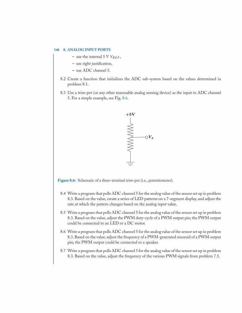
146 8. ANALOG INPUT PORTS
– use the internal 5 V VREF ,
– use right justification,
– use ADC channel 5.
8.2 Create a function that initializes the ADC sub-system based on the values determined inproblem 8.1.
8.3 Use a trim-pot (or any other reasonable analog sensing device) as the input to ADC channel5. For a simple example, see Fig. 8.6.
+5V
VA
Figure 8.6: Schematic of a three-terminal trim-pot (i.e., potentiometer).
8.4 Write a program that polls ADC channel 5 for the analog value of the sensor set up in problem8.3. Based on the value, create a series of LED patterns on a 7-segment display, and adjust therate at which the pattern changes based on the analog input value.
8.5 Write a program that polls ADC channel 5 for the analog value of the sensor set up in problem8.3. Based on the value, adjust the PWM duty-cycle of a PWM output pin; the PWM outputcould be connected to an LED or a DC motor.
8.6 Write a program that polls ADC channel 5 for the analog value of the sensor set up in problem8.3. Based on the value, adjust the frequency of a PWM-generated sinusoid of a PWM outputpin; the PWM output could be connected to a speaker.
8.7 Write a program that polls ADC channel 5 for the analog value of the sensor set up in problem8.3. Based on the value, adjust the frequency of the various PWM signals from problem 7.5.
147
C H A P T E R 9
Interrupt Processing
9.1 INTRODUCTIONAll processing performed in previous chapters has been completely deterministic. For example, anytime a program needed to retrieve an input signal, it did so by repeatedly checking the desiredinformation source, a process called polling. This concept is shown in Fig. 9.1. Each block in the
Function A
Function B
Main Loop
Figure 9.1: A conceptual view of software polling.
figure is meant to indicate a single instruction, and the solid directional lines show the path thatthe Program Counter (PC) follows. As can be seen in this example, the program executes MainLoop which makes two different function calls, one to Function A and one to Function B. Wehave already been able to create software that follows this topology in previous chapter problems.
While polling works fine, there are a couple of reasons to avoid it. First, performance can sufferin more complicated embedded systems which require input from many sources.For example, a high-tier cell-phone has to monitor an entire key-pad, menu buttons, ambient light sensor, QWERTYkeyboard, etc. When software is written such that the processor is constantly polling all inputs foractivity, it will never have a chance to perform other operations that generally control the behaviorof the device. Second, an important feature for many embedded systems is to periodically power-down hardware, a process called sleeping. When a processor sleeps, it is able to conserve power,which leads to longer portable battery lives. Many environments that involve polling don’t allow themicroprocessor to sleep at all, resulting in batteries draining much faster.
An alternative version to the polling example is shown in Fig. 9.2(a). Function A has beenmoved from the deterministic pathway of the polling software to an isolated function that gets called

148 9. INTERRUPT PROCESSING
in response to an interrupt condition. Interrupts are signals used to notify the CPU that some newevent has just occurred. Because most interrupt sources occur outside the CPU boundary, interrupts
ISR Function A
Function B
Main Loop
ISR Begin
ISR End
ISR Function A
Function B
Main Loop
ISR Begin
ISR End
(a) Program with ISR (b) ISR called from anywhere
Figure 9.2: A conceptual view of software containing an ISR. The interrupt signal may occur at anytime during the primary algorithm’s processing path.
may be thought of as random signals that can occur at any point during the otherwise predictable flowof the primary algorithm. When an interrupt occurs, the CPU stops whatever it is doing and jumpsto an associated Interrupt Service Routine (ISR). An ISR is a special function written to handle thefact that the interrupt signal occurred.This process is depicted in Fig. 9.2(b). In the polling example,Function A always occurred at the same time within the loop of processing. By contrast, the newexample algorithm has moved Function A processing outside the main algorithm’s path, reducingthe work constantly performed by the main program. The drawback is the added complexity of thefact that now Function A can be called at any time, and so software needs to be written with thisbehavior in mind.
9.1.1 CONTEXTThe software context may be defined as the CPU environment as seen by each assembly instruction.Typically, the context may be specified by the set of CPU registers, including the PC which pointsto the current assembly instruction. For the example interrupt-based algorithm to work properly,it is certainly necessary that Main Loop function as it did in the polling case. This requires thecurrent context to appear as though each assembly instruction is executed in the intended sequence.Interrupt processing is made possible by saving the context on ISR entry and restoring the contextwhen the ISR completes. For example, suppose an interrupt occurs at the third (machine) instruction
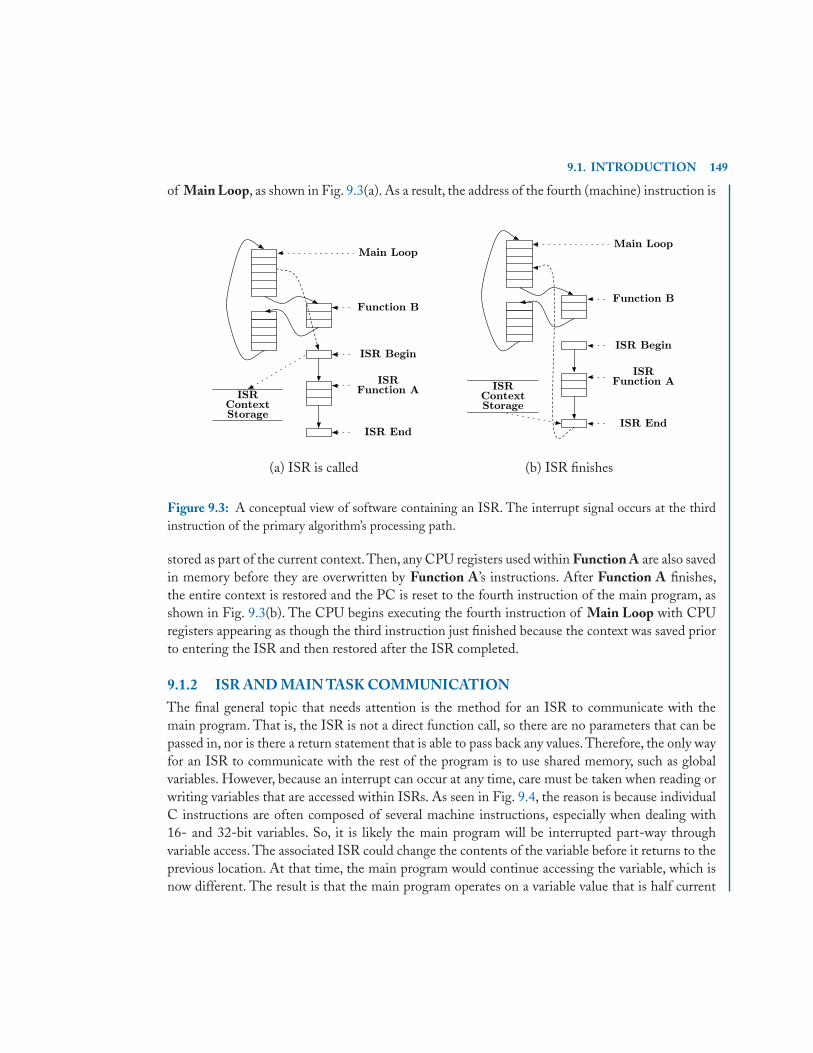
9.1. INTRODUCTION 149
of Main Loop, as shown in Fig. 9.3(a). As a result, the address of the fourth (machine) instruction is
ISR Function A
Function B
Main Loop
ISR Begin
ISR End
ISR Context Storage
ISR Function A
Function B
Main Loop
ISR Begin
ISR End
ISR Context Storage
(a) ISR is called (b) ISR finishes
Figure 9.3: A conceptual view of software containing an ISR. The interrupt signal occurs at the thirdinstruction of the primary algorithm’s processing path.
stored as part of the current context.Then, any CPU registers used within Function A are also savedin memory before they are overwritten by Function A’s instructions. After Function A finishes,the entire context is restored and the PC is reset to the fourth instruction of the main program, asshown in Fig. 9.3(b). The CPU begins executing the fourth instruction of Main Loop with CPUregisters appearing as though the third instruction just finished because the context was saved priorto entering the ISR and then restored after the ISR completed.
9.1.2 ISR AND MAIN TASK COMMUNICATIONThe final general topic that needs attention is the method for an ISR to communicate with themain program. That is, the ISR is not a direct function call, so there are no parameters that can bepassed in, nor is there a return statement that is able to pass back any values. Therefore, the only wayfor an ISR to communicate with the rest of the program is to use shared memory, such as globalvariables. However, because an interrupt can occur at any time, care must be taken when reading orwriting variables that are accessed within ISRs. As seen in Fig. 9.4, the reason is because individualC instructions are often composed of several machine instructions, especially when dealing with16- and 32-bit variables. So, it is likely the main program will be interrupted part-way throughvariable access. The associated ISR could change the contents of the variable before it returns to theprevious location. At that time, the main program would continue accessing the variable, which isnow different. The result is that the main program operates on a variable value that is half current

150 9. INTERRUPT PROCESSING
Atomic Machine Instructions
C Instruction Executing Instruction when Interrupt occurs
Figure 9.4: A single C instruction is composed of several machine instructions. This example shows aninterrupt signal occurring at the fifth machine instruction.
and half incorrect. In order to mitigate these problems, any memory that is shared between ISRs andthe main program need to be protected. The protection necessary is usually in the form of turningoff global interrupts before accessing the shared variable. When finished, the global interrupts needto be restored to their previous state.
9.1.3 ATMEGA328P INTERRUPTS IN CA great amount of care must be taken when writing ISR functions in assembly due to the contextmanagement. The same care must be taken when writing ISR functions in C. However, mostcompilers provide special macros or functions that cause the compiler to handle most of the contextmanagement. As a result, interrupt-based software does not look all that different from pollingsoftware.
In the case of the AVR-GCC compiler for the ATmega328P, there is a set of predefinedfunction names that correspond to every interrupt signal that can occur on the processor. When analgorithm needs to handle an interrupt, all that is required is to write the desired function usingthe appropriate function name. The entire list of interrupts and their associated function names arepresented in Table 9.1.
Aside from the specific ISR function name, there is a set of macros defined in the header fileavr/interrupt.h that are used to tell the compiler how to manage certain functions. ISR() is themost basic macro used to register and mark a function as an interrupt handler. The macro is definedto take the vector function name as its first parameter followed by optional attributes includingISR_BLOCK, ISR_NOBLOCK, ISR_NAKED and ISR_ALIASOF(vect). Each attribute provides thefollowing:
• ISR_BLOCK - (default behavior) identical to an ISR with no attributes specified. Global inter-rupts are disabled by the ATmega328P hardware when entering the ISR, without the compilermodifying this state.

9.1. INTRODUCTION 151
Table 9.1: ATmega328P InterruptsInterrupt ISR C
Pri. Address Source Function Name Description1 0x0000 RESET System reset (power-on)
2 0x0002 INT0 INT0_vect External Interrupt Request 0
3 0x0004 INT1 INT1_vect External Interrupt Request 1
4 0x0006 PCINT0 PCINT0_vect Pin Change Interrupt Request 0
5 0x0008 PCINT1 PCINT1_vect Pin Change Interrupt Request 1
6 0x000A PCINT2 PCINT2_vect Pin Change Interrupt Request 2
7 0x000C WDT WDT_vect Watchdog Time-out Interrupt
8 0x000E TIMER2 COMPA TIMER2_COMPA_vect Timer/Counter2 Compare Match A
9 0x0010 TIMER2 COMPB TIMER2_COMPB_vect Timer/Counter2 Compare Match B
10 0x0012 TIMER2 OVF TIMER2_OVF_vect Timer/Counter2 Overflow
11 0x0014 TIMER1 CAPT TIMER1_CAPT_vect Timer/Counter1 Capture Event
12 0x0016 TIMER1 COMPA TIMER1_COMPA_vect Timer/Counter1 Compare Match A
13 0x0018 TIMER1 COMPB TIMER1_COMPB_vect Timer/Counter1 Compare Match B
14 0x001A TIMER1 OVF TIMER1_OVF_vect Timer/Counter1 Overflow
15 0x001C TIMER0 COMPA TIMER0_COMPA_vect Timer/Counter0 Compare Match A
16 0x001E TIMER0 COMPB TIMER0_COMPB_vect Timer/Counter0 Compare Match B
17 0x0020 TIMER0 OVF TIMER0_OVF_vect Timer/Counter0 Overflow
18 0x0022 SPI, STC SPI_STC_vect SPI Serial Transfer Complete
19 0x0024 USART, RX USART_RX_vect USART Receive Complete
20 0x0026 USART, UDRE USART_UDRE_vect USART Data Register Empty
21 0x0028 USART, TX USART_TX_vect USART Transmit Complete
22 0x002A ADC ADC_vect ADC Conversion Complete
23 0x002C EE READY EE_READY_vect EEPROM Ready
24 0x002E ANALOG COMP ANALOG_COMP_vect Analog Comparator
25 0x0030 TWI TWI_vect 2-wire Serial Interface
26 0x0032 SPM READY SPM_READY_vect Store Program Memory Ready
• ISR_NOBLOCK - Global interrupts are reenabled by the compiler-generated code when the ISRis initially entered.This may be used to allow nested ISRs, meaning an ISR may be interruptedby a higher-priority interrupt.
• ISR_NAKED -The compiler does not generate any context management code.The ISR functionhas to explicitly save and restore the context, including adding the reti instruction at the endof the ISR to return the PC to is prior location.
• ISR_ALIASOF(vect) - The ISR is linked to the ISR specified by the vect parameter. Thisallows a single ISR function to handle multiple interrupt signals.

152 9. INTERRUPT PROCESSING
As an example, suppose we would like to enable the interrupt for Timer1 overflow. Once thetimer is set up (not shown), the interrupt is enabled with the following.
Example 9.1
###definedefinedefine TIMSK1_ADDR (unsignedunsignedunsigned charcharchar *) 0x6F
###definedefinedefine TIMSK1_ICIE_MASK 0x20###definedefinedefine TIMSK1_OCIEB_MASK 0x04###definedefinedefine TIMSK1_OCIEA_MASK 0x02###definedefinedefine TIMSK1_TOIE_MASK 0x01
unsignedunsignedunsigned longlonglong g_timerCount;
voidvoidvoid InitializeTimer (voidvoidvoid){
unsignedunsignedunsigned charcharchar *portTimerCounterInterruptMaskRegister;unsignedunsignedunsigned charcharchar shadow;
portTimerCounterInterruptMaskRegister = TIMSK1_ADDR;
shadow = *portTimerCounterInterruptMaskRegister;shadow &= ˜( TIMSK1_ICIE_MASK |
TIMSK1_OCIEB_MASK |TIMSK1_OCIEA_MASK |TIMSK1_TOIE_MASK);
shadow |= TIMSK1_TOIE_MASK;*portTimerCounterInterruptMaskRegister = shadow;
g_timerCount = 0;}
This code piece clears the four different interrupt bits before setting the single bit indicating the desireto receive interrupt signals whenever the overflow occurs in Timer1. The ISR may be somethinglike the following.
Example 9.2
ISR(TIMER1_OVF_vect){
g_timerCount ++;}
It is a rule-of-thumb not to perform extensive processing inside an ISR so as not to starve themain program. For example, function calls should not be made from within an ISR. Usually an ISR

9.1. INTRODUCTION 153
contains a few instructions that might set a global variable to indicate to the main program that thesignal has occurred. In this example, a global variable is incremented whenever the overflow occurs.
To complete the example, the main program needs to do something with the global variableset by the ISR. Because this is shared memory between the main program and the ISR, protectionneeds to be placed around the variable access to prevent the ISR from corrupting the value in thememory location. The protection is realized by turning off global interrupts before accessing thevariable. When finished, the global interrupts need to be restored to their previous state. This ismanaged via the I-bit in the SREG register such as in the following example.
Example 9.3
###definedefinedefine SREG_ADDR (unsignedunsignedunsigned charcharchar *) 0x5F
###definedefinedefine SREG_GLOBAL_INT_ENABLE 0x80
voidvoidvoid loop(){
unsignedunsignedunsigned charcharchar *statusRegister;unsignedunsignedunsigned charcharchar shadow;unsignedunsignedunsigned longlonglong timerCountCopy;
/*Save the current global interrupt bit value in shadow.
*/statusRegister = SREG_ADDR;shadow = *statusRegister;
/*Disable global interrupts.
*/*statusRegister &= ˜SREG_GLOBAL_INT_ENABLE;
/* access g_timerCount here */timerCountCopy = g_timerCount;
/*Restore the global interrupt bit to previous value.
*/ififif (( shadow & SREG_GLOBAL_INT_ENABLE) == SREG_GLOBAL_INT_ENABLE){
*statusRegister |= SREG_GLOBAL_INT_ENABLE;}
/* Now do stuff on the copy of the g_timerCount variable */}

154 9. INTERRUPT PROCESSING
9.2 PERTINENT REGISTER DESCRIPTIONSThe information presented in this section was taken from ATMEL (2009).
9.2.1 EICRA - EXTERNAL INTERRUPT CONTROL REGISTER A
Bit 7 6 5 4 3 2 1 00x69 - - - - ISC11 ISC10 ISC01 ISC00
Read/Write R R R R R/W R/W R/W R/WDefault 0 0 0 0 0 0 0 0
• ISC11-0: Interrupt Sense Control 1 Bit 1 and Bit 0.
• ISC01-0: Interrupt Sense Control 0 Bit 1 and Bit 0. The External Interrupt x is activated bythe external pin INTx if the SREG I-flag and the corresponding interrupt mask are set. Thelevel and edges on the external INTx pin that activate the interrupt are defined in Table 9.1.The value on the INTx pin is sampled before detecting edges. If edge or toggle interrupt isselected, pulses that last longer than one clock period will generate an interrupt. Shorter pulsesare not guaranteed to generate an interrupt. If low level interrupt is selected, the low level mustbe held until the completion of the currently executing instruction to generate an interrupt.
Table 9.2: Interrupt x Sense ControlISCx1-0 Description
00 The low level of INTx generates an interrupt request.01 Any logical change on INTx generates an interrupt request.10 The falling edge of INTx generates an interrupt request.11 The rising edge of INTx generates an interrupt request.
9.2.2 EIMSK - EXTERNAL INTERRUPT MASK REGISTER
Bit 7 6 5 4 3 2 1 00x3D - - - - - - INT1 INT0
Read/Write R R R R R R R/W R/WDefault 0 0 0 0 0 0 0 0
• INT1: External Interrupt Request 1 Enable.
• INT0: External Interrupt Request 0 Enable. When the INTx bit is set (one) and the I-bitin the Status Register (SREG) is set (one), the external pin interrupt is enabled. The InterruptSense Control bits 1/0 (ISCx1:0) in the External Interrupt Control Register A (EICRA) definewhether the external interrupt is activated on the rising and/or falling edge of the INTx pinor level sensed. Activity on the pin will cause an interrupt request even if INTx is configured
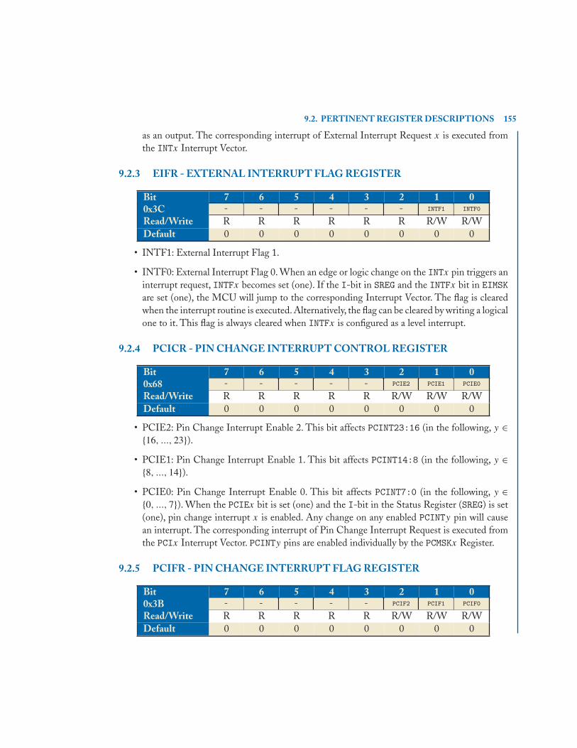
9.2. PERTINENT REGISTER DESCRIPTIONS 155
as an output. The corresponding interrupt of External Interrupt Request x is executed fromthe INTx Interrupt Vector.
9.2.3 EIFR - EXTERNAL INTERRUPT FLAG REGISTER
Bit 7 6 5 4 3 2 1 00x3C - - - - - - INTF1 INTF0
Read/Write R R R R R R R/W R/WDefault 0 0 0 0 0 0 0 0
• INTF1: External Interrupt Flag 1.
• INTF0: External Interrupt Flag 0. When an edge or logic change on the INTx pin triggers aninterrupt request, INTFx becomes set (one). If the I-bit in SREG and the INTFx bit in EIMSKare set (one), the MCU will jump to the corresponding Interrupt Vector. The flag is clearedwhen the interrupt routine is executed. Alternatively, the flag can be cleared by writing a logicalone to it. This flag is always cleared when INTFx is configured as a level interrupt.
9.2.4 PCICR - PIN CHANGE INTERRUPT CONTROL REGISTER
Bit 7 6 5 4 3 2 1 00x68 - - - - - PCIE2 PCIE1 PCIE0
Read/Write R R R R R R/W R/W R/WDefault 0 0 0 0 0 0 0 0
• PCIE2: Pin Change Interrupt Enable 2. This bit affects PCINT23:16 (in the following, y ∈{16, ..., 23}).
• PCIE1: Pin Change Interrupt Enable 1. This bit affects PCINT14:8 (in the following, y ∈{8, ..., 14}).
• PCIE0: Pin Change Interrupt Enable 0. This bit affects PCINT7:0 (in the following, y ∈{0, ..., 7}). When the PCIEx bit is set (one) and the I-bit in the Status Register (SREG) is set(one), pin change interrupt x is enabled. Any change on any enabled PCINTy pin will causean interrupt. The corresponding interrupt of Pin Change Interrupt Request is executed fromthe PCIx Interrupt Vector. PCINTy pins are enabled individually by the PCMSKx Register.
9.2.5 PCIFR - PIN CHANGE INTERRUPT FLAG REGISTER
Bit 7 6 5 4 3 2 1 00x3B - - - - - PCIF2 PCIF1 PCIF0
Read/Write R R R R R R/W R/W R/WDefault 0 0 0 0 0 0 0 0

156 9. INTERRUPT PROCESSING
• PCIF2: Pin Change Interrupt Flag 2. This bit affects PCINT23:16 (in the following, y ∈{16, ..., 23}).
• PCIF1: Pin Change Interrupt Flag 1. This bit affects PCINT14:8 (in the following, y ∈{8, ..., 14}).
• PCIF0: Pin Change Interrupt Flag 0. This bit affects PCINT7:0 (in the following, y ∈{0, ..., 7}). When a logic change on any PCINTy pin triggers an interrupt request, PCIFxbecomes set (one). If the I-bit in SREG and the PCIEx bit in PCICR are set (one), the MCUwill jump to the corresponding Interrupt Vector.The flag is cleared when the interrupt routineis executed. Alternatively, the flag can be cleared by writing a logical one to it.
9.2.6 PCMSK2 - PIN CHANGE MASK REGISTER 2
Bit 7 6 5 4 3 2 1 00x6D PCINT23 PCINT22 PCINT21 PCINT20 PCINT19 PCINT18 PCINT17 PCINT16
Read/Write R/W R/W R/W R/W R/W R/W R/W R/WDefault 0 0 0 0 0 0 0 0
• PCINT23-16: Pin Change Enable Mask 23-16. Each PCINT23:16-bit selects whether pinchange interrupt is enabled on the corresponding I/O pin. If PCINT23:16 is set and thePCIE2 bit in PCICR is set, pin change interrupt is enabled on the corresponding I/O pin. IfPCINT23:16 is cleared, pin change interrupt on the corresponding I/O pin is disabled.
9.2.7 PCMSK1 - PIN CHANGE MASK REGISTER 1
Bit 7 6 5 4 3 2 1 00x6C - PCINT14 PCINT13 PCINT12 PCINT11 PCINT10 PCINT9 PCINT8
Read/Write R R/W R/W R/W R/W R/W R/W R/WDefault 0 0 0 0 0 0 0 0
• PCINT14-8:Pin Change Enable Mask 14-8.EachPCINT14:8-bit selects whether pin changeinterrupt is enabled on the corresponding I/O pin. If PCINT14:8 is set and the PCIE1 bit inPCICR is set, pin change interrupt is enabled on the corresponding I/O pin. If PCINT14:8 iscleared, pin change interrupt on the corresponding I/O pin is disabled.
9.2.8 PCMSK0 - PIN CHANGE MASK REGISTER 0
Bit 7 6 5 4 3 2 1 00x6B PCINT7 PCINT6 PCINT5 PCINT4 PCINT3 PCINT2 PCINT1 PCINT0
Read/Write R/W R/W R/W R/W R/W R/W R/W R/WDefault 0 0 0 0 0 0 0 0

9.2. PERTINENT REGISTER DESCRIPTIONS 157
• PCINT7-0: Pin Change Enable Mask 7-0. Each PCINT7:0-bit selects whether pin changeinterrupt is enabled on the corresponding I/O pin. If PCINT7:0 is set and the PCIE0 bit inPCICR is set, pin change interrupt is enabled on the corresponding I/O pin. If PCINT7:0 iscleared, pin change interrupt on the corresponding I/O pin is disabled.
9.2.9 TIMSK0 - TIMER/COUNTER0 INTERRUPT MASK REGISTER
Bit 7 6 5 4 3 2 1 00x6E - - - - - OCIE0B OCIE0A TOIE0
Read/Write R R R R R R/W R/W R/WDefault 0 0 0 0 0 0 0 0
• OCIE0B: Timer/Counter0 Output Compare Match Channel B Interrupt Enable. When theOCIE0B bit is written to one, and the I-bit in the Status Register (SREG) is set, the Timer/-Counter0 Compare Match B interrupt is enabled. The corresponding interrupt is executed ifa Compare Match in Timer/Counter0 on channel B occurs, i.e., when the OCF0B bit is set inthe Timer/Counter0 Interrupt Flag Register (TIFR0).
• OCIE0A: Timer/Counter0 Output Compare Match Channel A Interrupt Enable. Whenthe OCIE0A bit is written to one, and the I-bit in the Status Register (SREG) is set, theTimer/Counter0 Compare Match A interrupt is enabled. The corresponding interrupt isexecuted if a Compare Match in Timer/Counter0 on channel A occurs, i.e., when the OCF0Abit is set in the Timer/Counter0 Interrupt Flag Register (TIFR0).
• TOIE0: Timer/Counter0 Overflow Interrupt Enable. When the TOIE0 bit is written to one,and the I-bit in the Status Register (SREG) is set, the Timer/Counter0 Overflow interrupt isenabled. The corresponding interrupt is executed if an overflow in Timer/Counter0 occurs,i.e., when the TOV0 bit is set in the Timer/Counter0 Interrupt Flag Register (TIFR0).
9.2.10 TIFR0 - TIMER/COUNTER0 INTERRUPT FLAG REGISTER
Bit 7 6 5 4 3 2 1 00x35 - - - - - OCF0B OCF0A TOV0
Read/Write R R R R R R/W R/W R/WDefault 0 0 0 0 0 0 0 0
• OCF0B: Timer/Counter0 Output Compare Match Channel B Flag. The OCF0B bit is setwhen a Compare Match occurs between the Timer/Counter0 and the data in OCR0B. OCF0B iscleared by hardware when executing the corresponding interrupt handling vector.Alternatively,OCF0B is cleared by writing a logic one to the flag.When the I-bit in SREG,OCIE0B, and OCF0Bare set, the Timer/Counter0 Compare Match B Interrupt is executed.
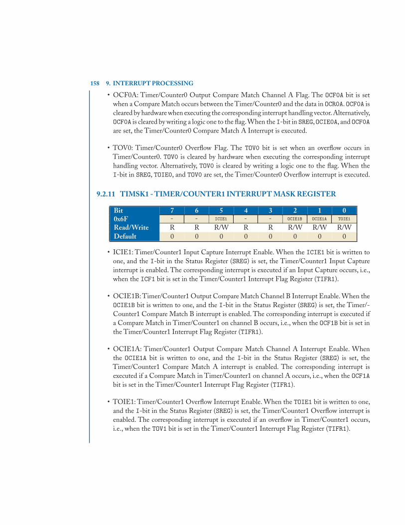
158 9. INTERRUPT PROCESSING
• OCF0A: Timer/Counter0 Output Compare Match Channel A Flag. The OCF0A bit is setwhen a Compare Match occurs between the Timer/Counter0 and the data in OCR0A. OCF0A iscleared by hardware when executing the corresponding interrupt handling vector.Alternatively,OCF0A is cleared by writing a logic one to the flag.When the I-bit in SREG,OCIE0A, and OCF0Aare set, the Timer/Counter0 Compare Match A Interrupt is executed.
• TOV0: Timer/Counter0 Overflow Flag. The TOV0 bit is set when an overflow occurs inTimer/Counter0. TOV0 is cleared by hardware when executing the corresponding interrupthandling vector. Alternatively, TOV0 is cleared by writing a logic one to the flag. When theI-bit in SREG, TOIE0, and TOV0 are set, the Timer/Counter0 Overflow interrupt is executed.
9.2.11 TIMSK1 - TIMER/COUNTER1 INTERRUPT MASK REGISTER
Bit 7 6 5 4 3 2 1 00x6F - - ICIE1 - - OCIE1B OCIE1A TOIE1
Read/Write R R R/W R R R/W R/W R/WDefault 0 0 0 0 0 0 0 0
• ICIE1: Timer/Counter1 Input Capture Interrupt Enable. When the ICIE1 bit is written toone, and the I-bit in the Status Register (SREG) is set, the Timer/Counter1 Input Captureinterrupt is enabled. The corresponding interrupt is executed if an Input Capture occurs, i.e.,when the ICF1 bit is set in the Timer/Counter1 Interrupt Flag Register (TIFR1).
• OCIE1B: Timer/Counter1 Output Compare Match Channel B Interrupt Enable. When theOCIE1B bit is written to one, and the I-bit in the Status Register (SREG) is set, the Timer/-Counter1 Compare Match B interrupt is enabled. The corresponding interrupt is executed ifa Compare Match in Timer/Counter1 on channel B occurs, i.e., when the OCF1B bit is set inthe Timer/Counter1 Interrupt Flag Register (TIFR1).
• OCIE1A: Timer/Counter1 Output Compare Match Channel A Interrupt Enable. Whenthe OCIE1A bit is written to one, and the I-bit in the Status Register (SREG) is set, theTimer/Counter1 Compare Match A interrupt is enabled. The corresponding interrupt isexecuted if a Compare Match in Timer/Counter1 on channel A occurs, i.e., when the OCF1Abit is set in the Timer/Counter1 Interrupt Flag Register (TIFR1).
• TOIE1: Timer/Counter1 Overflow Interrupt Enable. When the TOIE1 bit is written to one,and the I-bit in the Status Register (SREG) is set, the Timer/Counter1 Overflow interrupt isenabled. The corresponding interrupt is executed if an overflow in Timer/Counter1 occurs,i.e., when the TOV1 bit is set in the Timer/Counter1 Interrupt Flag Register (TIFR1).

9.2. PERTINENT REGISTER DESCRIPTIONS 159
9.2.12 TIFR1 - TIMER/COUNTER1 INTERRUPT FLAG REGISTER
Bit 7 6 5 4 3 2 1 00x36 - - ICF1 - - OCF1B OCF1A TOV1
Read/Write R R R/W R R R/W R/W R/WDefault 0 0 0 0 0 0 0 0
• ICF1: Timer/Counter1 Input Capture Flag. The ICF1 bit is set when a Capture event occurson the ICP1 pin. When the Input Capture Register (ICR1) is set by the WGM13:0 to be used asthe TOP value, the ICF1 flag is set when the counter reaches the TOP value. ICF1 is clearedby hardware when executing the corresponding interrupt handling vector. Alternatively, ICF1is cleared by writing a logic one to the flag. When the I-bit in SREG, ICIE1, and ICF1 are set,the Timer/Counter1 Capture Event Interrupt is executed.
• OCF1B: Timer/Counter1 Output Compare Match Channel B Flag. The OCF1B bit is setwhen a Compare Match occurs between the Timer/Counter1 and the data in OCR1B. OCF1B iscleared by hardware when executing the corresponding interrupt handling vector.Alternatively,OCF1B is cleared by writing a logic one to the flag.When the I-bit in SREG,OCIE1B, and OCF1Bare set, the Timer/Counter1 Compare Match B Interrupt is executed.
• OCF1A: Timer/Counter1 Output Compare Match Channel A Flag. The OCF1A bit is setwhen a Compare Match occurs between the Timer/Counter1 and the data in OCR1A. OCF1A iscleared by hardware when executing the corresponding interrupt handling vector.Alternatively,OCF1A is cleared by writing a logic one to the flag.When the I-bit in SREG,OCIE1A, and OCF1Aare set, the Timer/Counter1 Compare Match A Interrupt is executed.
• TOV1: Timer/Counter1 Overflow Flag. The TOV1 bit is set when an overflow occurs inTimer/Counter1. TOV1 is cleared by hardware when executing the corresponding interrupthandling vector. Alternatively, TOV1 is cleared by writing a logic one to the flag. When theI-bit in SREG, TOIE1, and TOV1 are set, the Timer/Counter1 Overflow interrupt is executed.
9.2.13 TIMSK2 - TIMER/COUNTER2 INTERRUPT MASK REGISTER
Bit 7 6 5 4 3 2 1 00x70 - - - - - OCIE2B OCIE2A TOIE2
Read/Write R R R R R R/W R/W R/WDefault 0 0 0 0 0 0 0 0
• OCIE2B: Timer/Counter2 Output Compare Match Channel B Interrupt Enable. When theOCIE2B bit is written to one, and the I-bit in the Status Register (SREG) is set, the Timer/-Counter2 Compare Match B interrupt is enabled. The corresponding interrupt is executed ifa Compare Match in Timer/Counter2 on channel B occurs, i.e., when the OCF2B bit is set inthe Timer/Counter2 Interrupt Flag Register (TIFR2).
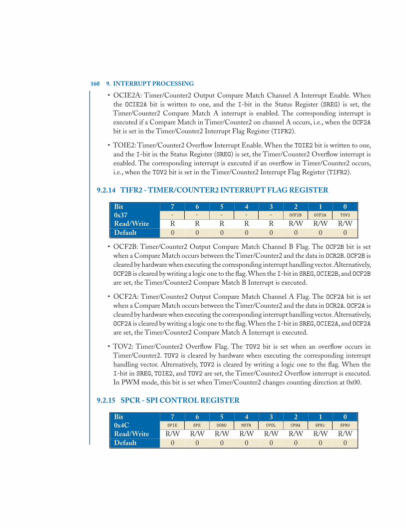
160 9. INTERRUPT PROCESSING
• OCIE2A: Timer/Counter2 Output Compare Match Channel A Interrupt Enable. Whenthe OCIE2A bit is written to one, and the I-bit in the Status Register (SREG) is set, theTimer/Counter2 Compare Match A interrupt is enabled. The corresponding interrupt isexecuted if a Compare Match in Timer/Counter2 on channel A occurs, i.e., when the OCF2Abit is set in the Timer/Counter2 Interrupt Flag Register (TIFR2).
• TOIE2: Timer/Counter2 Overflow Interrupt Enable. When the TOIE2 bit is written to one,and the I-bit in the Status Register (SREG) is set, the Timer/Counter2 Overflow interrupt isenabled. The corresponding interrupt is executed if an overflow in Timer/Counter2 occurs,i.e., when the TOV2 bit is set in the Timer/Counter2 Interrupt Flag Register (TIFR2).
9.2.14 TIFR2 - TIMER/COUNTER2 INTERRUPT FLAG REGISTER
Bit 7 6 5 4 3 2 1 00x37 - - - - - OCF2B OCF2A TOV2
Read/Write R R R R R R/W R/W R/WDefault 0 0 0 0 0 0 0 0
• OCF2B: Timer/Counter2 Output Compare Match Channel B Flag. The OCF2B bit is setwhen a Compare Match occurs between the Timer/Counter2 and the data in OCR2B. OCF2B iscleared by hardware when executing the corresponding interrupt handling vector.Alternatively,OCF2B is cleared by writing a logic one to the flag.When the I-bit in SREG,OCIE2B, and OCF2Bare set, the Timer/Counter2 Compare Match B Interrupt is executed.
• OCF2A: Timer/Counter2 Output Compare Match Channel A Flag. The OCF2A bit is setwhen a Compare Match occurs between the Timer/Counter2 and the data in OCR2A. OCF2A iscleared by hardware when executing the corresponding interrupt handling vector.Alternatively,OCF2A is cleared by writing a logic one to the flag.When the I-bit in SREG,OCIE2A, and OCF2Aare set, the Timer/Counter2 Compare Match A Interrupt is executed.
• TOV2: Timer/Counter2 Overflow Flag. The TOV2 bit is set when an overflow occurs inTimer/Counter2. TOV2 is cleared by hardware when executing the corresponding interrupthandling vector. Alternatively, TOV2 is cleared by writing a logic one to the flag. When theI-bit in SREG, TOIE2, and TOV2 are set, the Timer/Counter2 Overflow interrupt is executed.In PWM mode, this bit is set when Timer/Counter2 changes counting direction at 0x00.
9.2.15 SPCR - SPI CONTROL REGISTER
Bit 7 6 5 4 3 2 1 00x4C SPIE SPE DORD MSTR CPOL CPHA SPR1 SPR0
Read/Write R/W R/W R/W R/W R/W R/W R/W R/WDefault 0 0 0 0 0 0 0 0
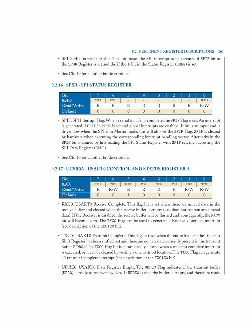
9.2. PERTINENT REGISTER DESCRIPTIONS 161
• SPIE: SPI Interrupt Enable. This bit causes the SPI interrupt to be executed if SPIF bit inthe SPSR Register is set and the if the I-bit in the Status Register (SREG) is set.
• See Ch. 10 for all other bit descriptions.
9.2.16 SPSR - SPI STATUS REGISTER
Bit 7 6 5 4 3 2 1 00x4D SPIF WCOL - - - - - SPI2X
Read/Write R R R R R R R R/WDefault 0 0 0 0 0 0 0 0
• SPIF: SPI Interrupt Flag.When a serial transfer is complete, the SPIF Flag is set. An interruptis generated if SPIE in SPCR is set and global interrupts are enabled. If SS is an input and isdriven low when the SPI is in Master mode, this will also set the SPIF Flag. SPIF is clearedby hardware when executing the corresponding interrupt handling vector. Alternatively, theSPIF bit is cleared by first reading the SPI Status Register with SPIF set, then accessing theSPI Data Register (SPDR).
• See Ch. 10 for all other bit descriptions.
9.2.17 UCSR0A - USART0 CONTROL AND STATUS REGISTER A
Bit 7 6 5 4 3 2 1 00xC0 RXC0 TXC0 UDRE0 FE0 DOR0 UPE0 U2X0 MPCM0
Read/Write R R/W R R R R R/W R/WDefault 0 0 1 0 0 0 0 0
• RXC0: USART0 Receive Complete. This flag bit is set when there are unread data in thereceive buffer and cleared when the receive buffer is empty (i.e., does not contain any unreaddata). If the Receiver is disabled, the receive buffer will be flushed and, consequently, the RXC0bit will become zero. The RXC0 Flag can be used to generate a Receive Complete interrupt(see description of the RXCIE0 bit).
• TXC0: USART0 Transmit Complete.This flag bit is set when the entire frame in the TransmitShift Register has been shifted out and there are no new data currently present in the transmitbuffer (UDR0). The TXC0 Flag bit is automatically cleared when a transmit complete interruptis executed, or it can be cleared by writing a one to its bit location.The TXC0 Flag can generatea Transmit Complete interrupt (see description of the TXCIE0 bit).
• UDRE0: USART0 Data Register Empty. The UDRE0 Flag indicates if the transmit buffer(UDR0) is ready to receive new data. If UDRE0 is one, the buffer is empty, and therefore ready
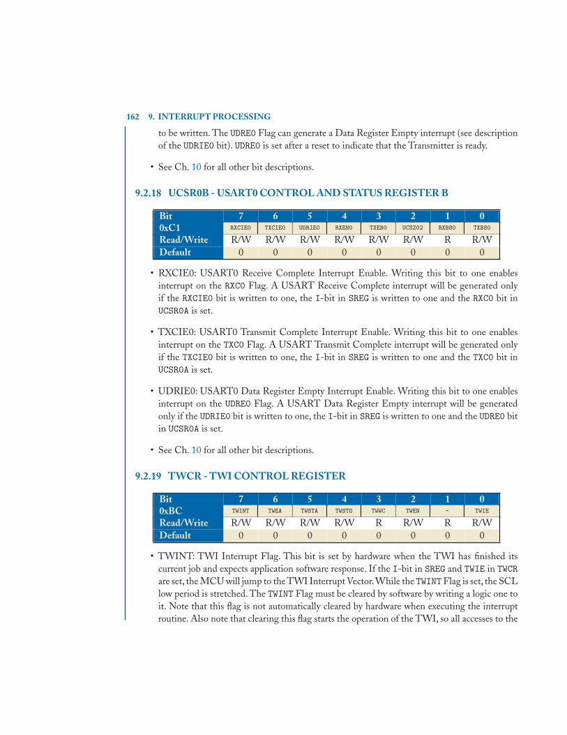
162 9. INTERRUPT PROCESSING
to be written. The UDRE0 Flag can generate a Data Register Empty interrupt (see descriptionof the UDRIE0 bit). UDRE0 is set after a reset to indicate that the Transmitter is ready.
• See Ch. 10 for all other bit descriptions.
9.2.18 UCSR0B - USART0 CONTROL AND STATUS REGISTER B
Bit 7 6 5 4 3 2 1 00xC1 RXCIE0 TXCIE0 UDRIE0 RXEN0 TXEN0 UCSZ02 RXB80 TXB80
Read/Write R/W R/W R/W R/W R/W R/W R R/WDefault 0 0 0 0 0 0 0 0
• RXCIE0: USART0 Receive Complete Interrupt Enable. Writing this bit to one enablesinterrupt on the RXC0 Flag. A USART Receive Complete interrupt will be generated onlyif the RXCIE0 bit is written to one, the I-bit in SREG is written to one and the RXC0 bit inUCSR0A is set.
• TXCIE0: USART0 Transmit Complete Interrupt Enable. Writing this bit to one enablesinterrupt on the TXC0 Flag. A USART Transmit Complete interrupt will be generated onlyif the TXCIE0 bit is written to one, the I-bit in SREG is written to one and the TXC0 bit inUCSR0A is set.
• UDRIE0: USART0 Data Register Empty Interrupt Enable. Writing this bit to one enablesinterrupt on the UDRE0 Flag. A USART Data Register Empty interrupt will be generatedonly if the UDRIE0 bit is written to one, the I-bit in SREG is written to one and the UDRE0 bitin UCSR0A is set.
• See Ch. 10 for all other bit descriptions.
9.2.19 TWCR - TWI CONTROL REGISTER
Bit 7 6 5 4 3 2 1 00xBC TWINT TWEA TWSTA TWSTO TWWC TWEN - TWIE
Read/Write R/W R/W R/W R/W R R/W R R/WDefault 0 0 0 0 0 0 0 0
• TWINT: TWI Interrupt Flag. This bit is set by hardware when the TWI has finished itscurrent job and expects application software response. If the I-bit in SREG and TWIE in TWCRare set, the MCU will jump to the TWI Interrupt Vector.While the TWINTFlag is set, the SCLlow period is stretched. The TWINT Flag must be cleared by software by writing a logic one toit. Note that this flag is not automatically cleared by hardware when executing the interruptroutine. Also note that clearing this flag starts the operation of the TWI, so all accesses to the

9.2. PERTINENT REGISTER DESCRIPTIONS 163
TWI Address Register (TWAR), TWI Status Register (TWSR), and TWI Data Register (TWDR)must be complete before clearing this flag.
• TWIE: TWI Interrupt Enable. When this bit is written to one, and the I-bit in SREG is set,the TWI interrupt request will be activated for as long as the TWINT Flag is high.
• See Ch. 10 for all other bit descriptions.
9.2.20 ADCSRA - ADC CONTROL AND STATUS REGISTER A
Bit 7 6 5 4 3 2 1 00x7A ADEN ADSC ADATE ADIF ADIE ADPS2 ADPS1 ADPS0
Read/Write R/W R/W R/W R/W R/W R/W R/W R/WDefault 0 0 0 0 0 0 0 0
• ADIF: ADC Interrupt Flag. This bit is set when an ADC conversion completes and the dataregisters are updated. The ADC conversion complete interrupt is executed if the ADIE bitand the I-bit in SREG are set. ADIF is cleared by hardware when executing the correspondinginterrupt handling vector. Alternatively, ADIF is cleared by writing a logical one to the flag.Beware that if doing a Read-Modify-Write on ADCSRA, a pending interrupt can be disabled.This also applies if the SBI and CBI instructions are used.
• ADIE: ADC Interrupt Enable. When this bit is written to one and the I-bit in SREG is set,the ADC conversion complete interrupt is activated.
• See Ch. 8 for all other bit descriptions.
9.2.21 ACSR - ANALOG COMPARATOR CONTROL AND STATUS REGISTER
Bit 7 6 5 4 3 2 1 00x50 ACD ACBG ACO ACIF ACIE ACIC ACIS1 ACIS0
Read/Write R/W R/W R R/W R/W R/W R/W R/WDefault 0 0 - 0 0 0 0 0
• ACIF: Analog Comparator Interrupt Flag. This bit is set by hardware when a comparatoroutput event triggers the interrupt mode defined by ACIS1:0. The Analog Comparator in-terrupt routine is executed if the ACIE bit is set and the I-bit in SREG is set. ACIF is clearedby hardware when executing the corresponding interrupt handling vector. Alternatively, ACIFis cleared by writing a logic one to the flag.
• ACIE: Analog Comparator Interrupt Enable. When this bit is written to one and the I-bitin SREG is set, the Analog Comparator interrupt is activated. When written logic zero, theinterrupt is disabled.
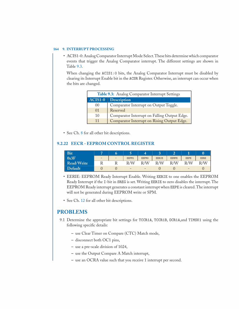
164 9. INTERRUPT PROCESSING
• ACIS1-0:Analog Comparator Interrupt Mode Select.These bits determine which comparatorevents that trigger the Analog Comparator interrupt. The different settings are shown inTable 9.3.
When changing the ACIS1:0 bits, the Analog Comparator Interrupt must be disabled byclearing its Interrupt Enable bit in the ACSR Register. Otherwise, an interrupt can occur whenthe bits are changed.
Table 9.3: Analog Comparator Interrupt SettingsACIS1-0 Description
00 Comparator Interrupt on Output Toggle.01 Reserved10 Comparator Interrupt on Falling Output Edge.11 Comparator Interrupt on Rising Output Edge.
• See Ch. 8 for all other bit descriptions.
9.2.22 EECR - EEPROM CONTROL REGISTER
Bit 7 6 5 4 3 2 1 00x3F - - EEPM1 EEPM0 EERIE EEMPE EEPE EERE
Read/Write R R R/W R/W R/W R/W R/W R/WDefault 0 0 - - 0 0 - 0
• EERIE: EEPROM Ready Interrupt Enable. Writing EERIE to one enables the EEPROMReady Interrupt if the I-bit in SREG is set. Writing EERIE to zero disables the interrupt. TheEEPROM Ready interrupt generates a constant interrupt when EEPE is cleared.The interruptwill not be generated during EEPROM write or SPM.
• See Ch. 12 for all other bit descriptions.
PROBLEMS9.1 Determine the appropriate bit settings for TCCR1A, TCCR1B, OCR1A,and TIMSK1 using the
following specific details:
– use Clear Timer on Compare (CTC) Match mode,
– disconnect both OC1 pins,
– use a pre-scale division of 1024,
– use the Output Compare A Match interrupt,
– use an OCRA value such that you receive 1 interrupt per second.
9.2. PERTINENT REGISTER DESCRIPTIONS 165
9.2 Create a function that initializes timer 1 based on the values determined in problem 9.1.
9.3 Create an ISR for timer 1.
9.4 Determine the appropriate bit settings for PCICR and PCMSK2 using the following specificdetails:
– use Port D4 as an input pin,
– disable the internal pull-up resistor,
– using Port D4 corresponds to Pin Change interrupt 20.
9.5 Create a function that initializes the Pin Change interrupt based on the values determined inproblem 9.4.
9.6 Create an ISR for Pin Change interrupt 20.
9.7 Create a program that utilizes the timer interrupt and the pin change interrupt in order tomeasure the frequency of a periodic signal on Port Pin D4. You can do this by saving andthen clearing a counter each time the timer interrupt occurs (at a rate of once per second).Additionally, you can increment the counter by the number of low-to-high and high-to-lowtransitions on pin D4 with the pin change interrupt. Your main loop should monitor whenthe timer interrupt goes off, and then write the frequency to the serial port for the user to see.Note: your setup function should call your two initialization functions, and then enable globalinterrupts in the SREG register.
9.8 Connect a controllable signal generator source to port pin D4. Warning: you should calibratethe signal before connecting it to the Arduino. Do so by connecting the signal generator to anoscilloscope and verify you have a 0-to-5V source. Be sure to note the frequency.
Use the program created in problem 9.7. Compare your output with that determined by theoscilloscope. Note: don’t forget the pin change interrupt occurs on both rising and fallingedges, so you will need to account for that in your output to the user.

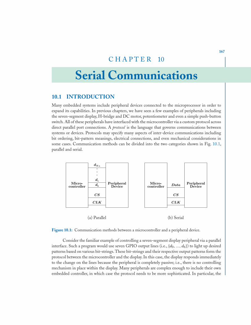
167
C H A P T E R 10
Serial Communications
10.1 INTRODUCTIONMany embedded systems include peripheral devices connected to the microprocessor in order toexpand its capabilities. In previous chapters, we have seen a few examples of peripherals includingthe seven-segment display, H-bridge and DC motor, potentiometer and even a simple push-buttonswitch. All of these peripherals have interfaced with the microcontroller via a custom protocol acrossdirect parallel port connections. A protocol is the language that governs communications betweensystems or devices. Protocols may specify many aspects of inter-device communications includingbit ordering, bit-pattern meanings, electrical connections, and even mechanical considerations insome cases. Communication methods can be divided into the two categories shown in Fig. 10.1,parallel and serial.
Micro-controller d0
dN-1
Peripheral Device
CS
CLK
.
.
.
d1Micro-
controller Data Peripheral Device
CS
CLK
(a) Parallel (b) Serial
Figure 10.1: Communication methods between a microcontroller and a peripheral device.
Consider the familiar example of controlling a seven-segment display peripheral via a parallelinterface. Such a program would use seven GPIO output lines (i.e., {d0, ..., d6}) to light up desiredpatterns based on various bit-strings.These bit-strings and their respective output patterns form theprotocol between the microcontroller and the display. In this case, the display responds immediatelyto the change on the lines because the peripheral is completely passive; i.e., there is no controllingmechanism in place within the display. Many peripherals are complex enough to include their ownembedded controller, in which case the protocol needs to be more sophisticated. In particular, the

168 10. SERIAL COMMUNICATIONS
microcontroller is considered the master while the embedded peripheral controller is consideredthe slave. The master device drives communications by controlling the chip select CS line(s) andthe synchronous clock CLK line. Any slave peripheral connected to the communication bus willwait until the master issues a signal, at which time the slave will perform the indicated function.Common examples of sophisticated peripherals that requires a parallel data bus are liquid crystaldisplays (LCDs) which contain hundreds or thousands of pixels. For a real example, consider someof the beautiful consumer electronic devices that are able to display high quality real-time video. Inorder to do so, they use a high data-rate throughput which requires a parallel data bus.
Most peripherals don’t have the requirement of large data-rate transfers, but they still needa method for sending and receiving bytes of information. An alternative to sending N bits at thesame time across N data lines is to transfer N bits one-at-a-time across a single data line as impliedin Fig. 10.1(b). Doing so reduces the number of external pins required by each peripheral’s packagethereby reducing chip sizes. This form of communication is called serial because each byte of infor-mation is used to create a series of bits, which is then transmitted and received along the data line.For example, suppose the microcontroller needs to send the eight-bit value 0x53 to the peripheral.Instead of using eight lines, the value is used to create the series {0, 1, 0, 1, 0, 0, 1, 1}. Then theCLK line is used by the microcontroller to tell the peripheral when the next bit in the series is readyto be sampled. The peripheral will shift in each bit when a CLK event occurs until all eight bitshave been received. It will then convert the series of bits back into the eight-bit byte. Notice thereare many questions that arise with this form of communication including:
• In what order are the series of bits shifted across the data line? Suppose the master transmitsthe most-significant bit (MSB) first, then the peripheral will receive the series in the order{0, 1, 0, 1, 0, 0, 1, 1}. Alternatively, the master could transmit the least-significant bit (LSB)first; in which case, the peripheral will receive the series {1, 1, 0, 0, 1, 0, 1, 0}. Either methodis fine, but the peripheral and master must agree before hand; otherwise, incorrect bytes willbe received.
• What constitutes a CLK event? The master could use either a falling-edge or a rising-edgeclock to specify a sampling signal to the peripheral device.
• How does the peripheral know when it is supposed to receive bytes and when it is supposedto transmit bytes?
All of these questions and many more are answered by the protocol. The two protocols I2C (pro-nounced“eye-squared see”) and SPI (pronounced“spy”) have become very common for a wide-varietyof peripheral integrated circuits (ICs) including EEPROM non-volatile memory, audio amplifiers,temperature sensors, H-bridge chips, and accelerometers. Many times, when embedded systems aredesigned with proprietary CPLDs or FPGAs, they will include one of these two serial protocols inorder to interact with the microcontroller. The following two sections present an overview of eachprotocol including specific information regarding the ATmega328P.

10.1. INTRODUCTION 169
10.1.1 INTER-INTEGRATED CIRCUITThe Inter-Integrated Circuit (I2C or IIC) serial protocol was created by NXP Semiconductors,originally a Philips semiconductor division, to attach low-speed peripherals to an embedded micro-processor as shown in Figure 10.2. I2C is a multi-point protocol in which more than two devices are
Micro-controller
Master
SDA
SCL
Peripheral Device
(1)
Slave
Peripheral Device (N-1)
Slave
Peripheral Device (N)
Slave
VDD
Figure 10.2: I2C serial communication method between a microcontroller master and one or more slaveperipheral devices.
able to communicate along the serial interface which is composed of a bidirectional serial data line(SDA) and a bidirectional serial clock (SCL). As a result, each line is configured as open-drain whichmeans that each must be pulled-up to VDD via an external resistor. Exactly one device on the bus isconsidered the master of the serial bus and all other devices are slaves. At the start of any serial trans-action, each slave listens to the bus for its own specific address.The master begins communication bytransmitting a single start bit followed by the unique 7-bit address of the slave device for which themaster is attempting to access, followed by read/write bit. The corresponding slave device respondswith an acknowledge bit if it is present on the serial bus. The master continues to issue clock eventson the SCL line and either receives information from the slave or writes information to the slavedepending on the read/write bit at the start of the session. The number of bits transferred during asingle session is dependent upon the peripheral device and the agreed-upon higher-level protocol.Notice that any device writing to SDA only needs to pull the line low for each ‘0’ written; otherwise,is leaves the line alone to write a ‘1’, which occurs due to the lines being pulled high externally. Anymanufacturer that includes the fully compatible protocol within their peripheral chip must pay afee in order to have an I2C slave address reserved by NXP, although the protocol itself is availablefree of charge. Some peripheral devices will provide a few external pins in order to “program” theI2C slave address via pull-up and pull-down resistors. In this way, an embedded system can havemultiple instances of the same component; for example, multiple temperature sensors from the same

170 10. SERIAL COMMUNICATIONS
manufacturer may co-exist on the same serial bus by programming each one with a unique addressusing pull-ups and pull-downs.
The ATmega328P provides an I2C serial interface via the 2-wire Serial Interface (TWI ).The bus allows for up to 128 different slave devices and up to 400 kHz data transfer speed. TheTWI provides an interrupt-based system in which an interrupt is issued after all bus events such asreception of a byte or transmission of a start condition. You will see how to manage a serial portthat utilizes interrupts later in the problems. The relevant TWI registers are listed in Sec. 10.2.Additionally, SDA and SCL use Port C pins 4 and 5 when configured to do so.
10.1.2 SERIAL PERIPHERAL INTERFACEThe Serial Peripheral Interface (SPI) serial protocol was created by Motorola to allow peripherals tocommunicate in full duplex mode as shown in Fig. 10.3. Full duplex means that two devices transmit
Micro-controller
Master
MOSI
MISO
Peripheral Device
(1)
Slave
Peripheral Device (N-1)
Slave
Peripheral Device (N)
Slave
SCLK
SS1SSN
Figure 10.3: SPI serial communication method between a microcontroller master and one or more slaveperipheral devices.
and receive data simultaneously (e.g., telephone communications), as opposed to half duplex whichmeans that two devices transmit and receive data by taking turns (e.g., public-safety radio commu-nications). SPI is another multi-point protocol in which devices communicate via the serial interfacecomposed of serial clock (SCLK), master-out/slave-in (MOSI ), master-in/slave-out (MISO) andslave-select (SS). Exactly one device on the bus is considered the master of the serial bus and allother devices are slaves. The master controls communication by asserting the SSi line of the ithslave device and then issues clock events on the SCLK line. The master simultaneously receivesinformation from the slave on MISO and writes information to the slave on MOSI . The meaning

10.1. INTRODUCTION 171
and number of bits transferred in both directions is dependent upon the peripheral device and theagreed-upon higher-level protocol.
The ATmega328P provides a SPI serial interface that allows for multiple peripheral deviceconnections. The SPI provides an interrupt-based system in which an interrupt is issued after eachbyte has been transmitted/received. When the ATmega328P processor is defined as the master, theprogram is responsible for managing each device’s slave select line prior to starting the communicationprocess. The relevant SPI registers are listed in Sec. 10.2. Additionally, SS, MOSI , MISO andSCK use Port B pins 2 through 5 when configured to do so. Note that SS is only used when theATmega328P is configured to be a slave device, it is not automatically controlled during masteroperation.
10.1.3 UNIVERSAL ASYNCHRONOUS RECEIVER/TRANSMITTERAnother common serial communications sub-circuit present on most microprocessors is a UniversalAsynchronous Receiver/Transmitter (UART), which is really just a fancy shift-register allowing forthe transformation between parallel and serial forms. UARTs provide both a receive (RX) and atransmit (T X) line, such as shown in Fig. 10.4. UARTs are the physical layer upon which differ-
Micro-controller
RX
TX Peripheral Device
Figure 10.4: UART serial communication method between a microcontroller and a peripheral device.
ent serial protocols operate including the multi-point Recommended Standard 485 (RS-485) andthe point-to-point RS-232 governed by the Electronic Industries Alliance (EIA). These commonstandards specify many aspects to the serial interface including voltage levels, connectors, pinouts,cable-lengths, bit orderings, and bit rates among others. One important difference in using a UARTversus I2C or SPI is the absence of a clock line to perform synchronization. Because there is nocommon clock signal, each device must search for a start bit by sampling its RX line with an internalclock. When the start bit is identified, the receiving device knows that a transmission has begunand can shift in the series of bits. Both transmitter and receiver must agree upon a common bit ratebefore communication begins; otherwise, the receiver will decode incorrect data.
10.1.4 USART ON ATMEGA328PThe ATmega328P provides a Universal Synchronous/Asynchronous Receiver/Transmitter (US-ART) that is configurable to allow for RS-232 communications. Further, the Arduino development
172 10. SERIAL COMMUNICATIONS
platform is designed such that the RX and T X lines connect to the FTDI USB-to-UART IC sothat software can be downloaded to the platform. In other words, you have already been making useof the ATmega328P UART in terms of development as well as all of the Serial-class function callsfor printing debugging information to the host computer’s serial terminal. The bootloader presentas part of the Arduino package configures the UART when power is applied to allow the host plat-form the ability to download new programs via USB. Because the USART is already connected to aperipheral device (the USB-to-UART converter chip), we will study how to manage a serial port insoftware by configuring the USART to perform RS-232 communications. The relevant USART0registers are listed in Sec. 10.2. Aside from the Arduino serial peripheral connection, the RXD,T XD and XCK signals use Port D pins 0, 1 and 4 when configured to do so. Note that XCK is aclock signal used in the synchronous mode of the USART hardware.
It is interesting that the ATmega328P uses the same physical address for both the inbound andthe outbound USART data registers (UDR0). The hardware is actually designed with two physicalregisters where CPU access controls which register is written-to or read-from via the single data-register address.
10.1.5 INTERRUPT-BASED SERIAL PORT MANAGEMENT IN CIt is very common for microprocessors to provide interrupt signals indicating when a single bytehas been received or has completed transmission. In either case, the associated ISR must movequickly to make room for the next incoming or outgoing byte. Additionally, the software needs toprovide enough allocated memory to hold the inbound and outbound messages. The amount ofspace necessary is defined by the application-level protocol. This means the engineer(s) responsiblefor defining the messages between the microcontroller and the peripheral should have a good ideawhat the largest single message will be and allocate the appropriate space accordingly. First, considerthe steps necessary for managing the serial port receiver using three global variables.
Example 10.1
###definedefinedefine USART_RECEIVE_BUFFER_SIZE 80
unsignedunsignedunsigned charcharchar g_receiveBuffer[USART_RECEIVE_BUFFER_SIZE ];unsignedunsignedunsigned charcharchar g_receiveHead;unsignedunsignedunsigned charcharchar g_receiveTail;
The g_receiveBuffer is the chunk of memory reserved to store the incoming data stream, andg_receiveHead and g_receiveTail are two indices used to write/read to/from the buffer. Whenused properly, these three variables form a circular buffer. As shown in Fig. 10.5, a circular buffer isan array treated as though the final element is succeeded by the first element. For example, pretendthe elements of the array are laid out in a circle such that the final entry is sitting next to the firstentry.
The following steps are used to manage the buffer.

10.1. INTRODUCTION 173
[0]
[1]
[N-1]
Head
Tail
Figure 10.5: Schematic view of an array used as a circular buffer.
1. Check if g_receiveHead == g_receiveTail; if they are equal, do nothing; otherwise, goto step 2.
2. Because the head and tail are different, we know the ISR has moved the head index. As aresult, we have some unprocessed bytes sitting in the receive buffer. Read the byte indicatedby the g_receiveTail index, and then increment the tail to the next byte in the buffer.
3. After incrementing g_receiveTail, check to make sure the value is not greater-than orequal-to the maximum value defined by the buffer array size. If it is, reset it back to 0.
These steps are implemented as in the following code pieces. Step one is the simple check performedin the infinite loop function.
Example 10.2
voidvoidvoid loop(){
unsignedunsignedunsigned charcharchar dataByte;
ififif (ReceivedBytes () > 0){
dataByte = GetNextReceivedByte ();
/* Do something with the received data byte here. */}
}

174 10. SERIAL COMMUNICATIONS
The function for checking the head and tail should look similar to the following; note thatglobal interrupts should be turned off prior to accessing the global head variable since the ISR willbe writing to that location.
Example 10.3
unsignedunsignedunsigned charcharchar ReceivedBytes (voidvoidvoid){
unsignedunsignedunsigned charcharchar receiveHead;unsignedunsignedunsigned charcharchar receivedBytes = 0;
/* Turn off global interrupts here. */
receiveHead = g_receiveHead;
/* Restore global interrupts here. */
ififif (receiveHead > g_receiveTail){
receivedBytes = receiveHead - g_receiveTail;}elseelseelse ififif (receiveHead < g_receiveTail){
/* Check the case that the head has circled around but the tailhasn’t. */
receivedBytes = receiveHead + (USART_RECEIVE_BUFFER_SIZE -g_receiveTail);
}
returnreturnreturn receivedBytes;}
Once it is known that the head and tail differ, reading the next byte in the buffer is managedsimilar to the following function.
Example 10.4
unsignedunsignedunsigned charcharchar GetNextReceivedByte (voidvoidvoid){
unsignedunsignedunsigned charcharchar receivedByte = 0;
ififif (ReceivedBytes () > 0){
receivedByte = g_receiveBuffer[g_receiveTail ++];
ififif (g_receiveTail >= USART_RECEIVE_BUFFER_SIZE)

10.1. INTRODUCTION 175
{g_receiveTail = 0;
}}
returnreturnreturn receivedByte;}
The final component to managing the serial port receiver is the ISR. When the receiveinterrupt occurs, the ISR needs to store the received byte into the head location of the receive buffer.The AVR-GCC ISR could look something like the following.
Example 10.5
###definedefinedefine UCSR0A_ADDR (unsignedunsignedunsigned charcharchar *) 0xC0###definedefinedefine UDR0_ADDR (unsignedunsignedunsigned charcharchar *) 0xC6
###definedefinedefine UCSR0A_RXC_MASK 0x80###definedefinedefine UCSR0A_RXC_EMPTY 0x00
ISR(USART_RX_vect){
unsignedunsignedunsigned charcharchar *portUSARTDataRegister;unsignedunsignedunsigned charcharchar *portUSARTControlAndStatusRegisterA;unsignedunsignedunsigned charcharchar shadow;
portUSARTDataRegister = UDR0_ADDR;portUSARTControlAndStatusRegisterA = UCSR0A_ADDR;
whilewhilewhile (((* portUSARTControlAndStatusRegisterA) & UCSR0A_RXC_MASK) !=UCSR0A_RXC_EMPTY)
{g_receiveBuffer[g_receiveHead ++] = *portUSARTDataRegister;
ififif (g_receiveHead >= USART_RECEIVE_BUFFER_SIZE){
g_receiveHead = 0;}
}}
Next, consider the steps necessary for managing the serial port transmitter. Note the processis mostly the inverse of the receive process; however, the transmission interrupt is only turned onwhile there are bytes to be sent. Three more global variables are needed.

176 10. SERIAL COMMUNICATIONS
Example 10.6
###definedefinedefine USART_TRANSMIT_BUFFER_SIZE 80
unsignedunsignedunsigned charcharchar g_transmitBuffer[USART_TRANSMIT_BUFFER_SIZE ];unsignedunsignedunsigned charcharchar g_transmitHead;unsignedunsignedunsigned charcharchar g_transmitTail;
As in the receiver case, the g_transmitBuffer is reserved memory used to store the outbounddata stream, and g_transmitHead and g_transmitTail are indices used to write/read to/fromthe buffer. The following steps are used to transmit a stream of bytes.
1. Write each new byte at g_transmitHead index, and then increment the head to the next bytein the buffer.
2. After incrementing g_transmitHead, check to make sure the value is not greater-than orequal-to the maximum value defined by the buffer array size. If it is, reset it back to 0.
3. Once the entire message is written to the buffer, turn on the transmitter by enabling the properinterrupt. Once the interrupt is enabled, the T X ISR will be called which will start the processof copying the transmit buffer bytes to the serial port transmitter.
These steps are implemented as in the following function.
Example 10.7
###definedefinedefine UCSR0B_ADDR (unsignedunsignedunsigned charcharchar *) 0xC1
###definedefinedefine UCSR0B_TXEN_MASK 0x08###definedefinedefine UCSR0B_TXEN_ON 0x08###definedefinedefine UCSR0B_TXEN_OFF 0x00
voidvoidvoid TransmitString (constconstconst charcharchar *bytes , unsignedunsignedunsigned charcharchar numberOfBytes){
unsignedunsignedunsigned charcharchar *portUSARTControlAndStatusRegisterB;unsignedunsignedunsigned charcharchar shadow;unsignedunsignedunsigned charcharchar i;
forforfor (i = 0; i < numberOfBytes; i++){
g_transmitBuffer[g_transmitHead ++] = (unsignedunsignedunsigned charcharchar) bytes[i];
ififif (g_transmitHead >= USART_TRANSMIT_BUFFER_SIZE){
g_transmitHead = 0;}
}
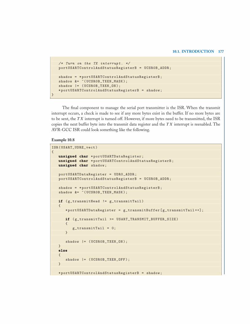
10.1. INTRODUCTION 177
/* Turn on the TX interrupt. */portUSARTControlAndStatusRegisterB = UCSR0B_ADDR;
shadow = *portUSARTControlAndStatusRegisterB;shadow &= ˜( UCSR0B_TXEN_MASK);shadow |= (UCSR0B_TXEN_ON);*portUSARTControlAndStatusRegisterB = shadow;
}
The final component to manage the serial port transmitter is the ISR. When the transmitinterrupt occurs, a check is made to see if any more bytes exist in the buffer. If no more bytes areto be sent, the T X interrupt is turned off. However, if more bytes need to be transmitted, the ISRcopies the next buffer byte into the transmit data register and the T X interrupt is reenabled. TheAVR-GCC ISR could look something like the following.
Example 10.8
ISR(USART_UDRE_vect){
unsignedunsignedunsigned charcharchar *portUSARTDataRegister;unsignedunsignedunsigned charcharchar *portUSARTControlAndStatusRegisterB;unsignedunsignedunsigned charcharchar shadow;
portUSARTDataRegister = UDR0_ADDR;portUSARTControlAndStatusRegisterB = UCSR0B_ADDR;
shadow = *portUSARTControlAndStatusRegisterB;shadow &= ˜( UCSR0B_TXEN_MASK);
ififif (g_transmitHead != g_transmitTail){
*portUSARTDataRegister = g_transmitBuffer[g_transmitTail ++];
ififif (g_transmitTail >= USART_TRANSMIT_BUFFER_SIZE){
g_transmitTail = 0;}
shadow |= (UCSR0B_TXEN_ON);}elseelseelse{
shadow |= (UCSR0B_TXEN_OFF);}
*portUSARTControlAndStatusRegisterB = shadow;

178 10. SERIAL COMMUNICATIONS
}
One important modification can be made to the code presented in order to make the ISRfunctions more efficient. Consider making the length of each buffer array a power of 2. Thenmanaging the indices can be made quicker by using a bit-mask as in the following example.
Example 10.9
###definedefinedefine USART_TRANSMIT_BUFFER_SIZE 32###definedefinedefine USART_TRANSMIT_BUFFER_MASK 0x1F
ISR(USART_UDRE_vect){
ififif (g_transmitHead != g_transmitTail){
*portUSARTDataRegister = g_transmitBuffer[g_transmitTail ++];
g_transmitTail &= USART_TRANSMIT_BUFFER_MASK;}
}
This concept can be taken one step further if the microcontroller has enough memory by letting eachbuffer be 256 bytes in length. Then, because an unsigned char is and 8-bit entity, the bit-mask isunnecessary as in the following example.
Example 10.10
###definedefinedefine USART_TRANSMIT_BUFFER_SIZE 256
ISR(USART_UDRE_vect){
ififif (g_transmitHead != g_transmitTail){
*portUSARTDataRegister = g_transmitBuffer[g_transmitTail ++];}
}
Now, when the head or tail is sitting at 255 and increased by one, it will naturally wrap around to0. Personally, I normally don’t like this kind of code as it represents poor maintainability; that is,given to a software developer, they would not automatically recognize that the wrap around willoccur. However, because we are dealing with ISRs, sometimes the low-level functionality is moreimportant than the maintainability of the software. Certainly this would be a valid location for anice comment stating the fact that the wrap around is intentional.

10.2. PERTINENT REGISTER DESCRIPTIONS 179
10.2 PERTINENT REGISTER DESCRIPTIONSThe information presented in this section was taken from ATMEL (2009).
10.2.1 TWBR - TWI BIT RATE REGISTER
Bit 7 6 5 4 3 2 1 00xB8 TWBR7 TWBR6 TWBR5 TWBR4 TWBR3 TWBR2 TWBR1 TWBR0
Read/Write R/W R/W R/W R/W R/W R/W R/W R/WDefault 0 0 0 0 0 0 0 0
• TWBR: TWI Bit Rate. TWBR selects the division factor for the bit rate generator. The bitrate generator is a frequency divider which generates the SCL clock frequency in the Mastermodes.
fSCL = 16 MHz16 + 2(TWBR)(PrescalerValue)
10.2.2 TWCR - TWI CONTROL REGISTER
Bit 7 6 5 4 3 2 1 00xBC TWINT TWEA TWSTA TWSTO TWWC TWEN - TWIE
Read/Write R/W R/W R/W R/W R R/W R R/WDefault 0 0 0 0 0 0 0 0
• TWEA:TWI Enable Acknowledge Bit.The TWEA bit controls the generation of the acknowl-edge pulse. If the TWEA bit is written to one, the ACK pulse is generated on the TWI bus ifthe following conditions are met.
1. The device’s own slave address has been received.
2. A general call has been received, while the TWGCE bit in the TWAR is set.
3. A data byte has been received in Master Receiver or Slave Receiver mode.
By writing the TWEA bit to zero, the device can be virtually disconnected from the 2-wireSerial Bus temporarily. Address recognition can then be resumed by writing the TWEA bit toone again.
• TWSTA: TWI START Condition Bit. The application writes the TWSTA bit to one when itdesires to become a Master on the 2-wire Serial Bus. The TWI hardware checks if the bus isavailable and generates a START condition on the bus if it is free. However, if the bus is notfree, the TWI waits until a STOP condition is detected and then generates a new STARTcondition to claim the bus Master status.TWSTAmust be cleared by software when the STARTcondition has been transmitted.

180 10. SERIAL COMMUNICATIONS
• TWSTO: TWI STOP Condition Bit. Writing the TWSTO bit to one in Master mode willgenerate a STOP condition on the 2-wire Serial Bus. When the STOP condition is executedon the bus, the TWSTO bit is cleared automatically. In Slave mode, setting the TWSTO bit canbe used to recover from an error condition. This will not generate a STOP condition, but theTWI returns to a well-defined unaddressed Slave mode and releases the SCL and SDA linesto a high impedance state.
• TWWC:TWI Write Collision Flag.The TWWC bit is set when attempting to write to the TWIData Register (TWDR) when TWINT is low. This flag is cleared by writing the TWDR Registerwhen TWINT is high.
• TWEN: TWI Enable Bit. The TWEN bit enables TWI operation and activates the TWIinterface. When TWEN is written to one, the TWI takes control over the I/O pins connected tothe SCL and SDA pins, enabling the slew-rate limiters and spike filters. If this bit is writtento zero, the TWI is switched off and all TWI transmissions are terminated, regardless of anyongoing operation.
• See Ch. 9 for interrupt-related bit descriptions.
10.2.3 TWSR - TWI STATUS REGISTER
Bit 7 6 5 4 3 2 1 00xB9 TWS7 TWS6 TWS5 TWS4 TWS3 - TWPS1 TWPS0
Read/Write R R R R R R R/W R/WDefault 1 1 1 1 1 0 0 0
• TWS7-3: TWI Status. These 5 bits reflect the status of the TWI logic and the 2-wire SerialBus. The different status codes are described later in this section. Note that the value readfrom TWSR contains both the 5-bit status value and the 2-bit pre-scaler value. The applicationdesigner should mask the pre-scaler bits to zero when checking the Status bits. This makesstatus checking independent of pre-scaler setting.
• TWPS1-0: TWI Pre-scaler Bits. These bits can be read and written, and control the bit ratepre-scaler.
10.2.4 TWDR - TWI DATA REGISTER
Bit 7 6 5 4 3 2 1 00xBB TWD7 TWD6 TWD5 TWD4 TWD3 TWD2 TWD1 TWD0
Read/Write R/W R/W R/W R/W R/W R/W R/W R/WDefault 1 1 1 1 1 1 1 1
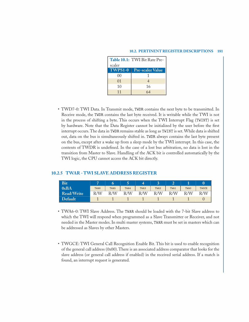
10.2. PERTINENT REGISTER DESCRIPTIONS 181
Table 10.1: TWI Bit Rate Pre-scalerTWPS1-0 Pre-scaler Value
00 101 410 1611 64
• TWD7-0: TWI Data. In Transmit mode, TWDR contains the next byte to be transmitted. InReceive mode, the TWDR contains the last byte received. It is writable while the TWI is notin the process of shifting a byte. This occurs when the TWI Interrupt Flag (TWINT) is setby hardware. Note that the Data Register cannot be initialized by the user before the firstinterrupt occurs.The data in TWDR remains stable as long as TWINT is set. While data is shiftedout, data on the bus is simultaneously shifted in. TWDR always contains the last byte presenton the bus, except after a wake up from a sleep mode by the TWI interrupt. In this case, thecontents of TWDR is undefined. In the case of a lost bus arbitration, no data is lost in thetransition from Master to Slave. Handling of the ACK bit is controlled automatically by theTWI logic, the CPU cannot access the ACK bit directly.
10.2.5 TWAR - TWI SLAVE ADDRESS REGISTER
Bit 7 6 5 4 3 2 1 00xBA TWA6 TWA5 TWA4 TWA3 TWA2 TWA1 TWA0 TWGCE
Read/Write R/W R/W R/W R/W R/W R/W R/W R/WDefault 1 1 1 1 1 1 1 0
• TWA6-0: TWI Slave Address. The TWAR should be loaded with the 7-bit Slave address towhich the TWI will respond when programmed as a Slave Transmitter or Receiver, and notneeded in the Master modes. In multi master systems, TWAR must be set in masters which canbe addressed as Slaves by other Masters.
• TWGCE: TWI General Call Recognition Enable Bit. This bit is used to enable recognitionof the general call address (0x00). There is an associated address comparator that looks for theslave address (or general call address if enabled) in the received serial address. If a match isfound, an interrupt request is generated.
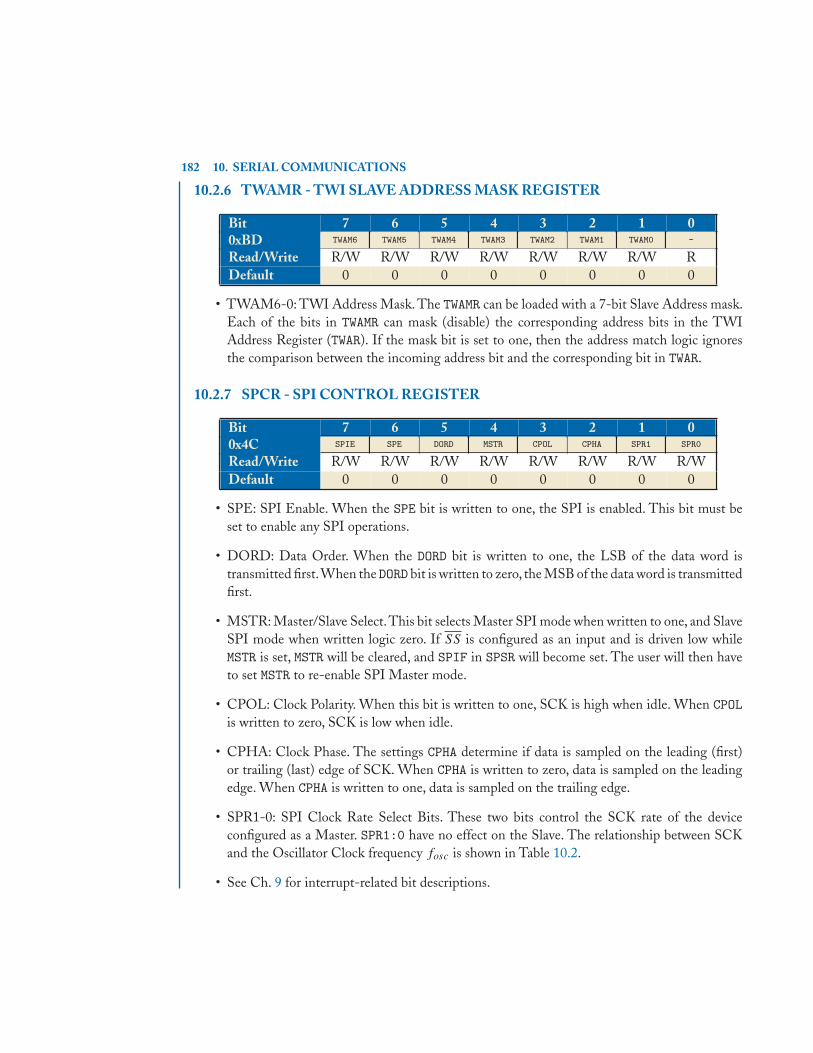
182 10. SERIAL COMMUNICATIONS
10.2.6 TWAMR - TWI SLAVE ADDRESS MASK REGISTER
Bit 7 6 5 4 3 2 1 00xBD TWAM6 TWAM5 TWAM4 TWAM3 TWAM2 TWAM1 TWAM0 -
Read/Write R/W R/W R/W R/W R/W R/W R/W RDefault 0 0 0 0 0 0 0 0
• TWAM6-0: TWI Address Mask. The TWAMR can be loaded with a 7-bit Slave Address mask.Each of the bits in TWAMR can mask (disable) the corresponding address bits in the TWIAddress Register (TWAR). If the mask bit is set to one, then the address match logic ignoresthe comparison between the incoming address bit and the corresponding bit in TWAR.
10.2.7 SPCR - SPI CONTROL REGISTER
Bit 7 6 5 4 3 2 1 00x4C SPIE SPE DORD MSTR CPOL CPHA SPR1 SPR0
Read/Write R/W R/W R/W R/W R/W R/W R/W R/WDefault 0 0 0 0 0 0 0 0
• SPE: SPI Enable. When the SPE bit is written to one, the SPI is enabled. This bit must beset to enable any SPI operations.
• DORD: Data Order. When the DORD bit is written to one, the LSB of the data word istransmitted first.When the DORD bit is written to zero, the MSB of the data word is transmittedfirst.
• MSTR: Master/Slave Select.This bit selects Master SPI mode when written to one, and SlaveSPI mode when written logic zero. If SS is configured as an input and is driven low whileMSTR is set, MSTR will be cleared, and SPIF in SPSR will become set. The user will then haveto set MSTR to re-enable SPI Master mode.
• CPOL: Clock Polarity. When this bit is written to one, SCK is high when idle. When CPOLis written to zero, SCK is low when idle.
• CPHA: Clock Phase. The settings CPHA determine if data is sampled on the leading (first)or trailing (last) edge of SCK. When CPHA is written to zero, data is sampled on the leadingedge. When CPHA is written to one, data is sampled on the trailing edge.
• SPR1-0: SPI Clock Rate Select Bits. These two bits control the SCK rate of the deviceconfigured as a Master. SPR1:0 have no effect on the Slave. The relationship between SCKand the Oscillator Clock frequency fosc is shown in Table 10.2.
• See Ch. 9 for interrupt-related bit descriptions.

10.2. PERTINENT REGISTER DESCRIPTIONS 183
Table 10.2: Relationship BetweenSCK and fosc.SPI2X SPR1-0 SCK Frequency
0 00 fosc/40 01 fosc/160 10 fosc/640 11 fosc/1281 00 fosc/21 01 fosc/81 10 fosc/321 11 fosc/64
10.2.8 SPSR - SPI STATUS REGISTER
Bit 7 6 5 4 3 2 1 00x4D SPIF WCOL - - - - - SPI2X
Read/Write R R R R R R R R/WDefault 0 0 0 0 0 0 0 0
• WCOL: Write COLlision Flag.The WCOL bit is set if the SPI Data Register (SPDR) is writtenduring a data transfer. The WCOL bit is cleared by first reading the SPI Status Register withWCOL set, and then accessing the SPI Data Register.
• SPI2X: Double SPI Speed Bit. When this bit is written logic one the SPI speed (SCKFrequency) will be doubled when the SPI is in Master mode. This means that the minimumSCK period will be two CPU clock periods. When the SPI is configured as Slave, the SPI isonly guaranteed to work at fosc/4 or lower.
• See Ch. 9 for interrupt-related bit descriptions.
10.2.9 SPDR - SPI DATA REGISTER
Bit 7 6 5 4 3 2 1 00x4E SPD7 SPD6 SPD5 SPD4 SPD3 SPD2 SPD1 SPD0
Read/Write R/W R/W R/W R/W R/W R/W R/W R/WDefault - - - - - - - -
• SPD7-0: SPI Data. The SPI Data Register is a read/write register used for data transferbetween the Register File and the SPI Shift Register. Writing to the register initiates datatransmission. Reading the register causes the Shift Register Receive buffer to be read.

184 10. SERIAL COMMUNICATIONS
10.2.10 UDR0 - USART0 I/O DATA REGISTER
Bit 7 6 5 4 3 2 1 00xC6 UD7 UD6 UD5 UD4 UD3 UD2 UD1 UD0
Read/Write R/W R/W R/W R/W R/W R/W R/W R/WDefault 0 0 0 0 0 0 0 0
• UD7-0: USART0 Data.The USART0 Transmit Data Buffer Register and USART0 ReceiveData Buffer Registers share the same I/O address referred to as USART0 Data Register orUDR0. The Transmit Data Buffer Register (TXB) will be the destination for data written to theUDR0 Register location. Reading the UDR0 Register location will return the contents of theReceive Data Buffer Register (RXB).
For 5-, 6-, or 7-bit characters the upper unused bits will be ignored by the Transmitter and setto zero by the Receiver.
The transmit buffer can only be written when the UDRE0 Flag in the UCSR0A Register isset. Data written to UDR0 when the UDRE0 Flag is not set, will be ignored by the USART0Transmitter. When data is written to the transmit buffer and the Transmitter is enabled, theTransmitter will load the data into the Transmit Shift Register when the Shift Register isempty. Then the data will be serially transmitted on the TxD0 pin.
The receive buffer consists of a two level FIFO. The FIFO will change its state whenever thereceive buffer is accessed. Due to this behavior of the receive buffer, do not use Read-Modify-Write instructions (SBI and CBI) on this location. Be careful when using bit test instructions(SBIC and SBIS) since these also will change the state of the FIFO.
10.2.11 UCSR0A - USART0 CONTROL AND STATUS REGISTER A
Bit 7 6 5 4 3 2 1 00xC0 RXC0 TXC0 UDRE0 FE0 DOR0 UPE0 U2X0 MPCM0
Read/Write R R/W R R R R R/W R/WDefault 0 0 1 0 0 0 0 0
• FE0: Frame Error. This bit is set if the next character in the receive buffer had a Frame Errorwhen received, i.e., when the first stop bit of the next character in the receive buffer is zero.This bit is valid until the receive buffer (UDR0) is read. The FE0 bit is zero when the stop bitof received data is one. Always set this bit to zero when writing to UCSR0A.
• DOR0: Data OverRun. This bit is set if a Data OverRun condition is detected. A DataOverRun occurs when the receive buffer is full (two characters), it is a new character waitingin the Receive Shift Register, and a new start bit is detected. This bit is valid until the receivebuffer (UDR0) is read. Always set this bit to zero when writing to UCSR0A.

10.2. PERTINENT REGISTER DESCRIPTIONS 185
• UPE0: USART0 Parity Error. This bit is set if the next character in the receive buffer had aParity Error when received and the Parity Checking was enabled at that point (UPM01 = 1).This bit is valid until the receive buffer (UDR0) is read. Always set this bit to zero when writingto UCSR0A.
• U2X0: Double the USART0Transmission Speed.This bit only has effect for the asynchronousoperation. Write this bit to zero when using synchronous operation.
Writing this bit to one will reduce the divisor of the baud rate divider from 16 to 8, effectivelydoubling the transfer rate for asynchronous communication.
• MPCM0: Multi-processor Communication Mode. This bit enables the Multi-processorCommunication mode. When the MPCM0 bit is written to one, all the incoming frames re-ceived by the USART0 Receiver that do not contain address information will be ignored. TheTransmitter is unaffected by the MPCM0 setting.
• See Ch. 9 for interrupt-related bit descriptions.
10.2.12 UCSR0B - USART0 CONTROL AND STATUS REGISTER B
Bit 7 6 5 4 3 2 1 00xC1 RXCIE0 TXCIE0 UDRIE0 RXEN0 TXEN0 UCSZ02 RXB80 TXB80
Read/Write R/W R/W R/W R/W R/W R/W R R/WDefault 0 0 0 0 0 0 0 0
• RXEN0: USART0 Receiver Enable. Writing this bit to one enables the USART0 Receiver.The Receiver will override normal port operation for the RxD0 pin when enabled. Disablingthe Receiver will flush the receive buffer invalidating the FE0, DOR0, and UPE0 Flags.
• TXEN0: USART0 Transmitter Enable. Writing this bit to one enables the USART0 Trans-mitter. The Transmitter will override normal port operation for the TxD0 pin when enabled.Disabling the Transmitter will not become effective until ongoing and pending transmissionsare completed, i.e., when the Transmit Shift Register and Transmit Buffer Register do notcontain data to be transmitted. When disabled, the Transmitter will no longer override theTxD0 port.
• UCSZ02: USART0 Character Size. The UCSZ02 bit combined with the UCSZ01:0 bits inUCSR0C sets the number of data bits (Character SiZe) in a frame the Receiver and Transmitteruse.
• RXB80: USART0 Receive Data Bit 8. RXB80 is the ninth data bit of the received characterwhen operating with serial frames with nine data bits. It must be read before reading the lowbits from UDR0.

186 10. SERIAL COMMUNICATIONS
• TXB80: USART0 Transmit Data Bit 8. TXB80 is the ninth data bit in the character to betransmitted when operating with serial frames with nine data bits. It must be written beforewriting the low bits to UDR0.
• See Ch. 9 for interrupt-related bit descriptions.
10.2.13 UCSR0C - USART0 CONTROL AND STATUS REGISTER C
Bit 7 6 5 4 3 2 1 00xC2 UMSEL01 UMSEL00 UPM01 UPM00 USBS0 UCSZ01 UCSZ00 UCPOL0
Read/Write R/W R/W R/W R/W R/W R/W R/W R/WDefault 0 0 0 0 0 1 1 0
• UMSEL01-0: USART0 Mode Select Bits. These bits select the mode of operation of theUSART0 as shown in Table 10.3.
Table 10.3: UMSEL0 Bit Settings.UMSEL01-0 Mode
00 Asynchronous USART01 Synchronous USART10 Reserved11 Master SPI (MSPIM)
• UPM01-0: USART0 Parity Mode. These bits enable and set type of parity generation andcheck. If enabled, the Transmitter will automatically generate and send the parity of thetransmitted data bits within each frame. The Receiver will generate a parity value for theincoming data and compare it to the UPM0 setting. If a mismatch is detected, the UPE0 Flagin UCSR0A will be set.
Table 10.4: UPM0 Bit Settings.UPM01-0 Parity Mode
00 Disabled01 Reserved10 Enabled, Even Parity11 Enabled, Odd Parity
• USBS0: USART0 Stop Bit Select. This bit selects the number of stop bits to be inserted bythe Transmitter. The Receiver ignores this setting. If USBS0 is cleared, there is 1 stop bit. IfUSBS0 is set, there are 2 stop bits.

10.2. PERTINENT REGISTER DESCRIPTIONS 187
• UCSZ01-0: USART0 Character Size. The UCSZ01:0 bits combined with the UCSZ02 bit inUCSR0B sets the number of data bits (Character SiZe) in a frame the Receiver and Transmitteruse.
Table 10.5: UCSZ0 BitSettings.
UCSZ02-0 Character Size000 5-bit001 6-bit010 7-bit011 8-bit100 Reserved101 Reserved110 Reserved111 9-bit
• UCPOL0: USART0 Clock Polarity. This bit is used for synchronous mode only. Write thisbit to zero when asynchronous mode is used. The UCPOL0 bit sets the relationship betweendata output change and data input sample, and the synchronous clock (XCK0).
Table 10.6: UCPOL0 Bit Settings.UCPOL0 Transmitted Data Changed Received Data Sampled
0 Rising XCK0 Edge Falling XCK0 Edge1 Falling XCK0 Edge Rising XCK0 Edge
10.2.14 UBRR0H AND UBRR0L - USART0 BAUD RATE REGISTERS
Bit 7 6 5 4 3 2 1 00xC5 - - - - UBRR0[11:8]
0xC4 UBRR0[7:0]
Read/Write R R R R R/W R/W R/W R/WR/W R/W R/W R/W R/W R/W R/W R/W
Default 0 0 0 0 0 0 0 0
• UBRR011-0: USART0 Baud Rate Bits.This is a 12-bit register which contains the USART0baud rate. The UBRR0H contains the four most significant bits, and the UBRR0L contains theeight least significant bits of the USART0 baud rate.Ongoing transmissions by theTransmitterand Receiver will be corrupted if the baud rate is changed. Writing UBRR0L will trigger animmediate update of the baud rate pre-scaler.

188 10. SERIAL COMMUNICATIONS
Table 10.7: UBRR0 Bit Settings for 16 MHz System Clock.Baud Rate (bps) U2X0 = 0, UBRR0 U2X0 = 1, UBRR0
2400 416 8324800 207 4169600 103 20714400 68 13819200 51 10328800 34 6838400 25 5157600 16 3476800 12 25115200 8 16230400 3 8250000 3 7500000 1 31000000 0 1
PROBLEMS10.1 Determine the appropriate bit settings for UCSR0A, UCSR0B, UCSR0C,and UBRR0 to manage a
serial interface using the following specific details:
– use normal transmission speed (i.e., disable the x2 speed),
– disable the multi-processor communication mode,
– turn on the RX complete interrupt, turn off the T X complete interrupt, turn on the dataregister empty interrupt,
– turn on the receiver, turn off the transmitter,
– set the character size to 8 bits,
– use the asynchronous USART mode,
– use no parity,
– use 1 stop bit,
– set the baud rate to 115200 bits per second.
10.2 Create a function that initializes the USART based on the values determined in problem 10.1.
10.3 Create an ISR for both the RX and T X interrupts.
10.4 Create a program that utilizes the USART to send and receive bytes via the USB converterchip to and from the host computer terminal program. Use a switch statement to send a
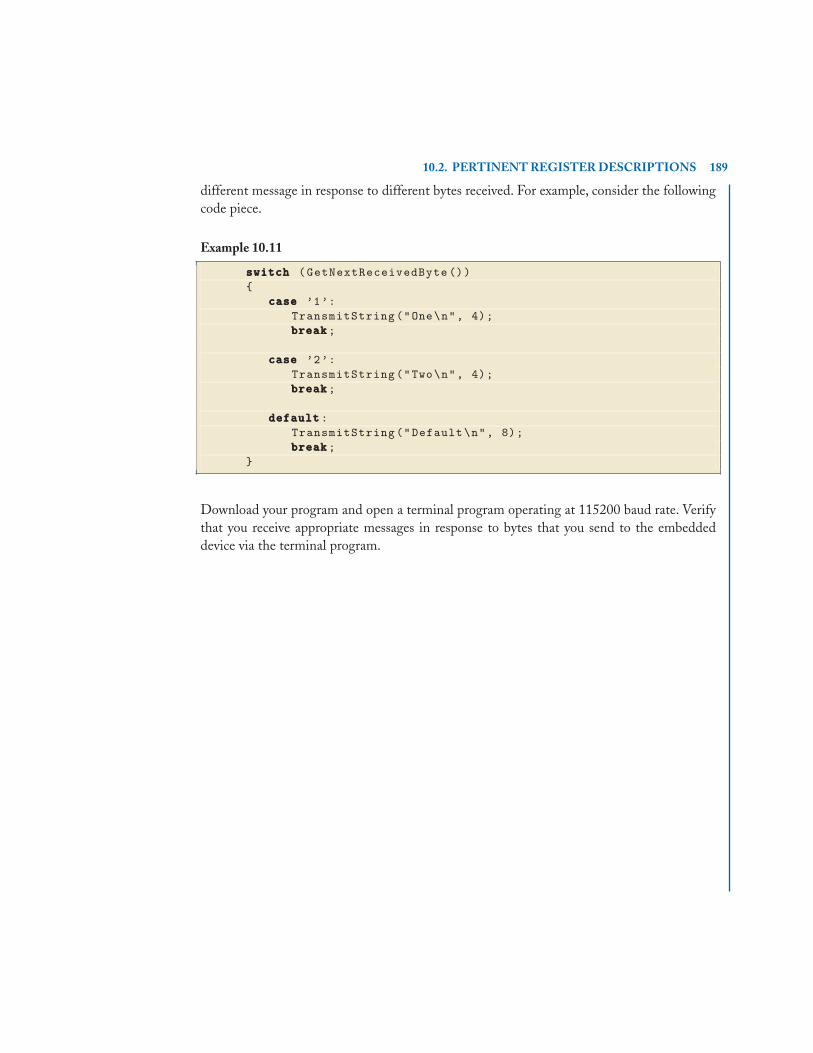
10.2. PERTINENT REGISTER DESCRIPTIONS 189
different message in response to different bytes received. For example, consider the followingcode piece.
Example 10.11
switchswitchswitch (GetNextReceivedByte ()){
casecasecase ’1’:TransmitString("One\n", 4);breakbreakbreak;
casecasecase ’2’:TransmitString("Two\n", 4);breakbreakbreak;
defaultdefaultdefault:TransmitString("Default\n", 8);breakbreakbreak;
}
Download your program and open a terminal program operating at 115200 baud rate. Verifythat you receive appropriate messages in response to bytes that you send to the embeddeddevice via the terminal program.


191
C H A P T E R 11
Assembly Language
11.1 INTRODUCTION
Up to this point, every program created has been via writing a high-level set of instructions describingthe behavior we want the microcontroller to follow. Sometimes, the instructions have been veryspecific, such as setting the address of a pointer to the location of some register, and then settingthe desired bit patterns via the pointer. However, many other blocks of code have been much moregeneral, such as creating loops or making sub-routine calls. By now, you probably have a goodunderstanding of how these behavioral descriptions function, but really such high-level instructionsare taken for granted. The reality is that a simple loop requires careful management of the loopvariable within a CPU register, and sub-routine calls need to keep track of parameters being passedin and out, return location, register preservation, etc. The biggest benefit of high-level languagesis that general behavior can be created in a source-code listing and processed with a set of toolsin order to generate a set of machine-level instructions that perform the intended operations. Themost common high-level language used in embedded systems is C and C++. One of the anomaliesin technology, C has been around since the 1970’s, and it doesn’t appear to be leaving any timesoon. Perhaps, the reason is that C is considered a low-level high-level language. Meaning, that Cis high-level enough to create behavioral descriptions in source code, yet C is low-level enough thatbit-wise operations can be performed on register contents in order to manipulate hardware directly.
The entire process of translating high-level source code into a machine-level program is shownin Fig. 11.1. The process begins by passing a source-code file file.c (or file.cpp) to the Prepro-cessor, whose job it is to manage all of the preprocessor directives. The two most common directivesare the #include and #define statements.The preprocessor scans the entire source file looking forthese statements. Each time it parses a #include<filei.h>, it replaces the preprocessor statementwith the contents of the file listed in the angle brackets, filei.h. Whenever the preprocessor readsa #define name value, it adds an entry to a preprocessor table such that whenever the phrase name
is found throughout the rest of the preprocessing stage, it is replaced by value. The preprocessortool continues this way until the entire file does not contain any more preprocessing commands; thatis, all have been replaced by their respective values.
The output of the preprocessor file.i (or file.ii) is provided as input to the Compiler,whose job it is to translate the general behavior and the specific statements into blocks of assemblyinstructions specific to the target processor. While the primary goal of the compiler is to create anassembly-code listing that will cause the desired behavior, a secondary objective is to be as efficientas possible. It is an important aspect of embedded systems to have programs with a very small foot-
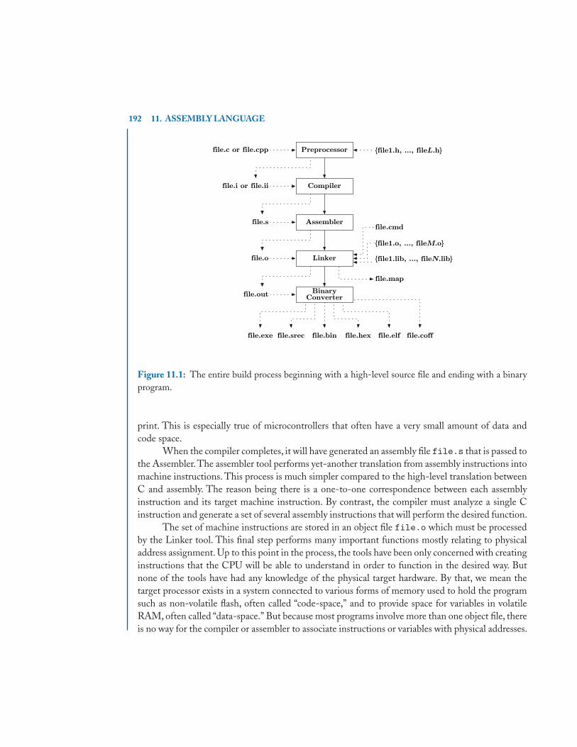
192 11. ASSEMBLY LANGUAGE
Compiler
Preprocessor
Assembler
Linker
Binary Converter
file.c or file.cpp {file1.h, ..., fileL.h}
file.i or file.ii
file.s
file.o
file.cmd
{file1.o, ..., fileM.o}
{file1.lib, ..., fileN.lib}
file.out
file.exe file.bin file.hex file.elffile.srec file.coff
file.map
Figure 11.1: The entire build process beginning with a high-level source file and ending with a binaryprogram.
print. This is especially true of microcontrollers that often have a very small amount of data andcode space.
When the compiler completes, it will have generated an assembly file file.s that is passed tothe Assembler.The assembler tool performs yet-another translation from assembly instructions intomachine instructions. This process is much simpler compared to the high-level translation betweenC and assembly. The reason being there is a one-to-one correspondence between each assemblyinstruction and its target machine instruction. By contrast, the compiler must analyze a single Cinstruction and generate a set of several assembly instructions that will perform the desired function.
The set of machine instructions are stored in an object file file.o which must be processedby the Linker tool. This final step performs many important functions mostly relating to physicaladdress assignment. Up to this point in the process, the tools have been only concerned with creatinginstructions that the CPU will be able to understand in order to function in the desired way. Butnone of the tools have had any knowledge of the physical target hardware. By that, we mean thetarget processor exists in a system connected to various forms of memory used to hold the programsuch as non-volatile flash, often called “code-space,” and to provide space for variables in volatileRAM, often called “data-space.” But because most programs involve more than one object file, thereis no way for the compiler or assembler to associate instructions or variables with physical addresses.
11.2. ARDUINO TOOL-CHAIN 193
Instead, the assembler will use relative addressing which will use a base address at the top of the file,and then offset deltas in-between each instruction or memory location. The linker will then take allof the object files and create a big table of function and memory labels, and assign physical addressesto all of the table entries. In order to do this, a special linker-command file file.cmd is passedin that contains all of the physical attributes of the target system, among other things. The otherthing the linker takes in is the set of any pre-built object libraries, for example the ANSI C functionprintf() can always be called by a program, but you never actually write the function yourself asthe functionality has already been built and is stored in a library file filei.lib.
The linker is often considered the final step in building the executable program file.out.However, many embedded systems require a special machine-code file format in order to downloadthe program. There are many programs that will convert from the linker output (.out) file formatinto a tool-required file format; for example, Motorola s-record (.srec), Common Object FileFormat (.coff), Executable and Linkable Format (.elf), Intel HEX (.hex), etc.
11.2 ARDUINO TOOL-CHAIN
The Arduino development environment, like any other integrated tool-chain, hides the details ofthe build process from the user. In fact, the concept of the Arduino tool is to hide as much aspossible from the software developer. This is evident by the fact that the tool only allows the userto create .pde files which are used to generate .cpp files before being processed and downloaded.Sometimes, this concept is useful, especially for a novice trying to learn embedded programming.However, eventually engineers need to be able to access the true set of steps in order to understandwhat is taking place within the system. Of particular interest is having the option to create hand-coded assembly programs. In general, it is best to develop software from a maintainable stand-point,which means “no assembly, ever”. The reason will become evident when you perform the chapterproblems – assembly programs are difficult for a human to easily comprehend and follow.Thus, theyare generally avoided because they present a challenge to maintain. However, there is still a need forsome assembly programming in the industry.
Typically, assembly will only find a place within Board Support Packages (BSPs), which aresets of low-level device driver functions necessary for Real-Time Operating Systems (RTOSes) tointerface properly with specific target microprocessors. Also, hand-coded assembly can still fill aneed in which there is a time-critical or space-limited situation. To understand why, imagine theprocess of translating prose from chinese to english, and then from english to spanish. Compare thatwith only one translation between english and spanish. The difference has to do with the fact thatenglish and spanish are generally similar, whereas chinese is generally very different—some dialectshave thousands of elements in their alphabet. While C compilers are generally very efficient, hand-coded assembly can always be made smaller and faster. As a personal example, several years ago I wasworking on a project for which there was a requirement that a Digital Signal Processor (DSP) processreal-time encryption using 1-bit cipher-feedback on a 48kHz data stream. This basically means48,000 encryption function calls needed to complete within 1 second. The encryption algorithm

194 11. ASSEMBLY LANGUAGE
was developed in C first, but there were not enough cycles available in the DSP to complete theprocessing in the required amount of time. So, I had to optimize the entire encryption process using100% assembly code. The result was satisfying at the time, but I doubt I would be able to maintainor even understand that source code today.
The Arduino Integrated Development Environment (IDE) does not allow the user to createan entire program out of assembly. However, the assembler and linker tools do exist on the hostcomputer, so it is just a matter of finding them and figuring out how to call them directly. The firststep is locating the programs on your computer. Assuming you installed the Arduino IDE in theApplications folder on MacOSX, or placed it at C:\ on Windows (XP), the path to the tools isgiven by:
• MacOSX:/Applications/Arduino.app/Contents/Resources/Java/hardware/tools/avr/bin
• Windows:C:\arduino-0018\hardware\tools\avr\bin
In order to access any of the programs, you need to:
• MacOSX: open /Applications/Utilities/Terminal
• Windows: open a cmd prompt by selecting Start→Run..., then typing cmd in the Open:field
For the rest of this section, let’s define the following “environmental variable,” so we don’t need tore-state the entire path for each file being accessed.
• MacOSX:{PAT H }=/Applications/Arduino.app/Contents/Resources/Java/hardware/tools/avr
• Windows:{PAT H }=C:\arduino-0018\hardware\tools\avrNow, for an example, consider the following C source-code file that blinks one of the LEDs
on the Arduino circuit-board. Beginning with the necessary #include and #defines.
Example 11.1
###includeincludeinclude <avr/interrupt.h>
###definedefinedefine TCCR1A_ADDR (unsignedunsignedunsigned charcharchar *) 0x80###definedefinedefine TCCR1A_COMA_MASK 0xC0###definedefinedefine TCCR1A_COMA_NORMAL 0x00###definedefinedefine TCCR1A_COMB_MASK 0x30###definedefinedefine TCCR1A_COMB_NORMAL 0x00###definedefinedefine TCCR1A_WGM_MASK 0x03###definedefinedefine TCCR1A_WGM_CTC 0x00
11.2. ARDUINO TOOL-CHAIN 195
###definedefinedefine TCCR1B_ADDR (unsignedunsignedunsigned charcharchar *) 0x81###definedefinedefine TCCR1B_WGM_MASK 0x18###definedefinedefine TCCR1B_WGM_CTC 0x08###definedefinedefine TCCR1B_CS_MASK 0x07###definedefinedefine TCCR1B_CS_OFF 0x00###definedefinedefine TCCR1B_CS_DIV_1 0x01###definedefinedefine TCCR1B_CS_DIV_8 0x02###definedefinedefine TCCR1B_CS_DIV_64 0x03###definedefinedefine TCCR1B_CS_DIV_256 0x04###definedefinedefine TCCR1B_CS_DIV_1024 0x05
###definedefinedefine OCR1AL_ADDR (unsignedunsignedunsigned charcharchar *) 0x88###definedefinedefine OCR1AH_ADDR (unsignedunsignedunsigned charcharchar *) 0x89###definedefinedefine OCR1A_ADDR (unsignedunsignedunsigned shortshortshort *) 0x88###definedefinedefine OCR1A_1_INT_PER_1_SEC (16000000 / 1024)
###definedefinedefine TIMSK1_ADDR (unsignedunsignedunsigned charcharchar *) 0x6F###definedefinedefine TIMSK1_ICIE_MASK 0x20###definedefinedefine TIMSK1_OCIEB_MASK 0x04###definedefinedefine TIMSK1_OCIEA_MASK 0x02###definedefinedefine TIMSK1_TOIE_MASK 0x01
###definedefinedefine SREG_ADDR (unsignedunsignedunsigned charcharchar *) 0x5F###definedefinedefine SREG_GLOBAL_INT_ENABLE 0x80
###definedefinedefine PORTB_DDR_ADDR (unsignedunsignedunsigned charcharchar *) 0x24###definedefinedefine PORTB_DATA_ADDR (unsignedunsignedunsigned charcharchar *) 0x25
###definedefinedefine LED_PIN_MASK 0x20
###definedefinedefine DELAY_IN_SECONDS 1
Next, we have the standard setup() and loop() functions used by the main() function.The Arduino IDE always generates and hides the main() function, so we need to explicitly add itas shown below.
Example 11.2
staticstaticstatic volatilevolatilevolatile unsignedunsignedunsigned charcharchar m_timerCount;
staticstaticstatic voidvoidvoid setup(voidvoidvoid);staticstaticstatic voidvoidvoid loop(voidvoidvoid);
intintint main(voidvoidvoid){
setup();

196 11. ASSEMBLY LANGUAGE
forforfor (;;){
loop();}
returnreturnreturn 0;}
/* *********************************************************** */
voidvoidvoid setup(voidvoidvoid){
unsignedunsignedunsigned charcharchar *statusRegister;statusRegister = SREG_ADDR;
*statusRegister &= ˜SREG_GLOBAL_INT_ENABLE;
InitializeOutput ();InitializeTimer ();
*statusRegister |= SREG_GLOBAL_INT_ENABLE;}
/* *********************************************************** */
voidvoidvoid loop(voidvoidvoid){
unsignedunsignedunsigned charcharchar *portData;
portData = PORTB_DATA_ADDR;
whilewhilewhile (m_timerCount < DELAY_IN_SECONDS);m_timerCount = 0;
*portData &= ˜LED_PIN_MASK;
whilewhilewhile (m_timerCount < DELAY_IN_SECONDS);m_timerCount = 0;
*portData |= LED_PIN_MASK;}
And the necessary functions to initialize the port pin output and the timer interrupt, and,finally, the timer1 ISR itself.

11.2. ARDUINO TOOL-CHAIN 197
Example 11.3
voidvoidvoid InitializeOutput (voidvoidvoid){
unsignedunsignedunsigned charcharchar *portDDR;unsignedunsignedunsigned charcharchar *portData;
portData = PORTB_DATA_ADDR;portDDR = PORTB_DDR_ADDR;
*portData |= LED_PIN_MASK;*portDDR |= LED_PIN_MASK;
}
/* *********************************************************** */
voidvoidvoid InitializeTimer (voidvoidvoid){
unsignedunsignedunsigned charcharchar *portTimerCounterControlRegisterA;unsignedunsignedunsigned charcharchar *portTimerCounterControlRegisterB;unsignedunsignedunsigned shortshortshort *portOutputCompareRegisterA;unsignedunsignedunsigned charcharchar *portTimerCounterInterruptMaskRegister;unsignedunsignedunsigned charcharchar shadow;
portTimerCounterControlRegisterA = TCCR1A_ADDR;portTimerCounterControlRegisterB = TCCR1B_ADDR;portOutputCompareRegisterA = OCR1A_ADDR;portTimerCounterInterruptMaskRegister = TIMSK1_ADDR;
shadow = *portTimerCounterControlRegisterA;shadow &= ˜( TCCR1A_COMA_MASK | TCCR1A_COMB_MASK | TCCR1A_WGM_MASK);shadow |= (TCCR1A_COMA_NORMAL | TCCR1A_COMB_NORMAL | TCCR1A_WGM_CTC);*portTimerCounterControlRegisterA = shadow;
shadow = *portTimerCounterControlRegisterB;shadow &= ˜( TCCR1B_CS_MASK | TCCR1B_WGM_MASK);shadow |= (TCCR1B_CS_DIV_1024 | TCCR1B_WGM_CTC);*portTimerCounterControlRegisterB = shadow;
*portOutputCompareRegisterA = OCR1A_1_INT_PER_1_SEC;
shadow = *portTimerCounterInterruptMaskRegister;shadow &= ˜( TIMSK1_ICIE_MASK | TIMSK1_OCIEB_MASK |
TIMSK1_OCIEA_MASK | TIMSK1_TOIE_MASK);shadow |= TIMSK1_OCIEA_MASK;*portTimerCounterInterruptMaskRegister = shadow;
m_timerCount = 0;}

198 11. ASSEMBLY LANGUAGE
/* *********************************************************** */
ISR(TIMER1_COMPA_vect){
m_timerCount ++;}
Once we create this BlinkInCTimer1.cpp file, we can create the machine object code byissuing the following commands at the appropriate command prompt (don’t forget to use the fullpath for the tool).
{PAT H }/bin/avr-gcc -g -Wall -O2 -mmcu=atmega328p -c BlinkInCTimer1.c
The result of this command will be the object file BlinkInCTimer1.o. That is, thepreprocessor, compiler, assembler and linker were all executed with this single step. The nextcommand is used to generate the BlinkInCTimer1.elf binary file format.
{PAT H }/bin/avr-gcc -g -Wall -O2 -mmcu=atmega328p -oBlinkInCTimer1.elf BlinkInCTimer1.o
An optional BlinkInCTimer1.map file containing the physical memory informa-tion for your program can be generated by adding the command-line argument -Wl,-Map,BlinkInCTimer1.map to the previous command (between -mmcu=atmega328p and -o was whereI put it). Note that the command is -Wl (‘el’ not ‘one’). Another program can be run in order togenerate a disassembly listing of your program:
{PAT H }/bin/avr-objdump -h -S BlinkInCTimer1.elf > BlinkInCTimer1.lst
This may be helpful when first learning how to create your own assembly-language programs.The final step necessary to create your program is to convert the .elf file into the .hex file formatwith the following command:
{PAT H }/bin/avr-objcopy -j .text -j .data -O ihex BlinkInCTimer1.elfBlinkInCTimer1.hex
Once your .hex file has been created, we need a way of downloading it to the target platform.Often, this requires an external hardware debugger; a separate device that connects your hostcomputer to the target platform. Alternatively, many embedded environments have a boot-loaderprogram installed on the target microprocessor. This little program is “permanent” as long as
11.3. ARDUINO ASSEMBLY 199
some catastrophic failure does not occur (e.g., erasing the entire flash). Its purpose is to providethe developer, a method for updating the main application as we have been doing all along withthe Arduino. The boot-loader has the ability to communicate with the host computer to receivecommands indicating that a new program is to be loaded. In the case that the program is alreadydownloaded, all the boot-loader does is jump to the entry point of the application. What this meansfor us is that we can download our new program via serial communication with the boot-loaderprogram, which is what the Arduino IDE does when you tell it to upload your program. Thecommand is given by:
{PAT H }/bin/avrdude -C [conff ile] -p m328p -c stk500v1 -P [serialport] -b57600 -D -U flash:w:BlinkInCTimer1.hex:i
where the configuration file is given by the path {PAT H }/etc/avrdude.conf and the serial portcan be found using the Arduino IDE under the Tools→Serial Port menu. Typically, this willbe something like:
• MacOSX: /dev/tty.usbserial-A900abQ1
• Windows: com3
If you issue the command, you should see a verbose listing of what the program is doing while it isconnected to the device. In particular, it should have written your program object code to the flash,and you should see the LED blink at a 1-second rate after you reset the board.
11.3 ARDUINO ASSEMBLYNow consider using only assembly instructions to perform the same blink functionality.The Arduinotool-chain allows for C-like preprocessor commands, so we can create constants just like in C.
Example 11.4
###includeincludeinclude <avr/interrupt.h>
###definedefinedefine TCCR1A_ADDR 0x80###definedefinedefine TCCR1A_VALUE 0x00
###definedefinedefine TCCR1B_ADDR 0x81###definedefinedefine TCCR1B_VALUE 0x0D
###definedefinedefine OCR1AL_ADDR 0x88###definedefinedefine OCR1AL_VALUE 0x09
###definedefinedefine OCR1AH_ADDR 0x89###definedefinedefine OCR1AH_VALUE 0x3D

200 11. ASSEMBLY LANGUAGE
###definedefinedefine TIMSK1_ADDR 0x6F###definedefinedefine TIMSK1_VALUE 0x02
###definedefinedefine PORTB_DDR_ADDR 0x24###definedefinedefine PORTB_DATA_ADDR 0x25
###definedefinedefine LED_PIN_MASK 0x20
###definedefinedefine DELAY_IN_SECONDS 1
The rest of the assembly description looks like the following (at least, this is my version of it).
Example 11.5
/*r16 = tempByter17 = timerFlagr18 = currentOutput
*/.section .text
/* *********************************************************** */
.global mainmain:
setup:cli
rcall InitializeOutputrcall InitializeTimer
sei
loop:
WaitToClear:cpi r17 , DELAY_IN_SECONDSbrne WaitToClear
clr r17
cbr r18 , LED_PIN_MASKsts PORTB_DATA_ADDR , r18
WaitToSet:cpi r17 , DELAY_IN_SECONDS

11.3. ARDUINO ASSEMBLY 201
brne WaitToSet
clr r17
sbr r18 , LED_PIN_MASKsts PORTB_DATA_ADDR , r18
rjmp loop
/* *********************************************************** */
InitializeOutput:ldi r18 , LED_PIN_MASKsts PORTB_DDR_ADDR , r18sts PORTB_DATA_ADDR , r18
ret
/* *********************************************************** */
InitializeTimer:ldi r16 , TCCR1A_VALUEsts TCCR1A_ADDR , r16
ldi r16 , TCCR1B_VALUEsts TCCR1B_ADDR , r16
ldi r17 , OCR1AH_VALUEldi r16 , OCR1AL_VALUEsts OCR1AH_ADDR , r17sts OCR1AL_ADDR , r16
ldi r16 , TIMSK1_VALUEsts TIMSK1_ADDR , r16
clr r17
ret
/* *********************************************************** */
.global TIMER1_COMPA_vectTIMER1_COMPA_vect:
inc r17reti
.end

202 11. ASSEMBLY LANGUAGE
One point about this program is the usage of specific registers to perform certain functions.Near the top of the source-code listing is a comment block detailing the fact that registers r16-r18are used for specific purposes. Because there is no compiler translation, then there is no mysteriousunder-cover register usage going on. Whatever we do with the registers is totally up to us. So, I havearbitrarily selected these three registers to always be used for the purpose of keeping track of someglobal memory. By doing this, I can reduce the number of instructions since I don’t need to reloadmemory every time I access a piece of information. The comment block is very helpful in remindingthe programmer which registers hold what values.
It is beyond the scope of this chapter to explain assembly-code programming further. Rather,the goal is to state how to set up the tools to build an object file given an assembly program.The list of all ATmega328P assembly instructions may be found in Apx. C. Additionally, variousaspects of assembly programming on the ATmega328P are detailed within the Arduino tool-chaindocumentation found at:
• MacOSX: {PAT H }/doc/avr-libc/assembler.html• Windows: {PAT H }\doc\avr-libc\avr-libc-user-manual\assembler.html
Once you create the file BlinkInAsmTimer1.S (note: the ‘S’ must be capital for the preprocessorto run on it), you can issue the same exact commands as in the case of the BlinkInCTimer1.cprogram.
11.4 ARDUINO INLINE ASSEMBLYNow that we have seen all the work involved in creating a program from direct assembly language, let’smove back to the Arduino IDE. We can use the Arduino editor to create pseudo-assembly programsby using inline assembly. Basically, we have the ability to insert specific assembly instructions intothe middle of C functions. There are a few new challenges including how to know what registers arealready being used by the compiler, and how to use variables declared in C in an assembly instruction,but we gain the benefit of using the Arduino IDE. Consider the following inline assembly programto perform the blink functionality, as before.
Example 11.6
###includeincludeinclude <avr/interrupt.h>
###definedefinedefine TCCR1A_ADDR 0x80###definedefinedefine TCCR1A_VALUE 0x00
###definedefinedefine TCCR1B_ADDR 0x81###definedefinedefine TCCR1B_VALUE 0x0D
###definedefinedefine OCR1AL_ADDR 0x88###definedefinedefine OCR1AL_VALUE 0x09

11.4. ARDUINO INLINE ASSEMBLY 203
###definedefinedefine OCR1AH_ADDR 0x89###definedefinedefine OCR1AH_VALUE 0x3D
###definedefinedefine TIMSK1_ADDR 0x6F###definedefinedefine TIMSK1_VALUE 0x02
###definedefinedefine PORTB_DDR_ADDR 0x24###definedefinedefine PORTB_DATA_ADDR 0x25
###definedefinedefine LED_PIN_MASK 0x20
###definedefinedefine DELAY_IN_SECONDS 1
/*r16 = tempByter17 = timerFlagr18 = currentOutput
*/
voidvoidvoid setup(){
asmasmasm volatilevolatilevolatile("cli\n\t""\n\t""ldi r18 , %[ theLedPinMask ]\n\t""sts %[ thePortBDdrAddress], r18\n\t""sts %[ thePortBDataAddress], r18\n\t""\n\t""ldi r16 , %[ theTccr1aValue ]\n\t""sts %[ theTccr1aAddress], r16\n\t""ldi r16 , %[ theTccr1bValue ]\n\t""sts %[ theTccr1bAddress], r16\n\t""ldi r17 , %[ theOcr1ahValue ]\n\t""ldi r16 , %[ theOcr1alValue ]\n\t""sts %[ theOcr1ahAddress], r17\n\t""sts %[ theOcr1alAddress], r16\n\t""ldi r16 , %[ theTimsk1Value ]\n\t""sts %[ theTimsk1Address], r16\n\t""clr r17\n\t""\n\t""sei\n\t""\n\t""1:" "cpi r17 , %[ theDelay ]\n\t""brne 1b\n\t""\n\t""clr r17\n\t""\n\t""cbr r18 , %[ theLedPinMask ]\n\t"
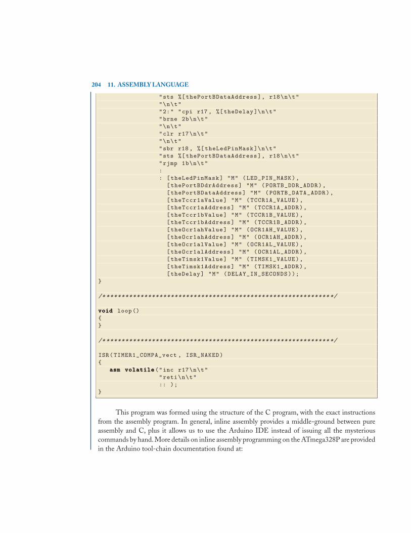
204 11. ASSEMBLY LANGUAGE
"sts %[ thePortBDataAddress], r18\n\t""\n\t""2:" "cpi r17 , %[ theDelay ]\n\t""brne 2b\n\t""\n\t""clr r17\n\t""\n\t""sbr r18 , %[ theLedPinMask ]\n\t""sts %[ thePortBDataAddress], r18\n\t""rjmp 1b\n\t":: [theLedPinMask] "M" (LED_PIN_MASK),
[thePortBDdrAddress] "M" (PORTB_DDR_ADDR),[thePortBDataAddress] "M" (PORTB_DATA_ADDR),[theTccr1aValue] "M" (TCCR1A_VALUE),[theTccr1aAddress] "M" (TCCR1A_ADDR),[theTccr1bValue] "M" (TCCR1B_VALUE),[theTccr1bAddress] "M" (TCCR1B_ADDR),[theOcr1ahValue] "M" (OCR1AH_VALUE),[theOcr1ahAddress] "M" (OCR1AH_ADDR),[theOcr1alValue] "M" (OCR1AL_VALUE),[theOcr1alAddress] "M" (OCR1AL_ADDR),[theTimsk1Value] "M" (TIMSK1_VALUE),[theTimsk1Address] "M" (TIMSK1_ADDR),[theDelay] "M" (DELAY_IN_SECONDS));
}
/* *********************************************************** */
voidvoidvoid loop(){}
/* *********************************************************** */
ISR(TIMER1_COMPA_vect , ISR_NAKED){
asmasmasm volatilevolatilevolatile("inc r17\n\t""reti\n\t":: );
}
This program was formed using the structure of the C program, with the exact instructionsfrom the assembly program. In general, inline assembly provides a middle-ground between pureassembly and C, plus it allows us to use the Arduino IDE instead of issuing all the mysteriouscommands by hand. More details on inline assembly programming on the ATmega328P are providedin the Arduino tool-chain documentation found at:

11.5. C-INSTRUCTION EFFICIENCY 205
• MacOSX: {PAT H }/doc/avr-libc/inline_asm.html• Windows: {PAT H }\doc\avr-libc\avr-libc-user-manual\inline_asm.html
Once you create the file BlinkInlineAsmTimer1.pde you can build and upload the program usingthe Arduino IDE just like you have done in all the previous chapter problems.
All three programs exhibited the desired 1-second blink control of the Arduino LED. Thedifference in program size is presented in Table 11.1. In order to compare the use of inline assemblyversus C, both programs were compiled using the command line and the Arduino IDE. As expected,the hand-coded assembly program is about half the size as any of the C programs.The next-smallestprogram is the C code using all inline assembly instructions being compiled using the command-lineinstructions. The command-line results are likely smaller due to an extra optimization parameterbeing turned on that may not be enabled within the IDE.
Table 11.1: Code size comparisons.Program Build Method Code-space BytesBlinkInAsmTimer1.S Command line 216BlinkInCTimer1.cpp Arduino IDE 582BlinkInlineAsmTimer1.cpp Arduino IDE 512BlinkInCTimer1.cpp Command line 406BlinkInlineAsmTimer1.cpp Command line 324
11.5 C-INSTRUCTION EFFICIENCYIt is always fortunate to have a high-level language compiler available for an embedded system. Tounderstand why this is true, consider the seemingly simple problem of adding two unsigned integerstogether. Let A = {a7a6a5a4a3a2a1a0} and B = {b7b6b5b4b3b2b1b0} be eight-bit vectors. Then, a“full adder” is a digital circuit that performs the addition of the ith stage
[ci,si] = ai + bi + ci−1
where si is called the ith sum bit and ci is the ith carry-out bit which is fed to the i + 1 stage asthe carry-in. Note that in this equation, + is one-bit addition, not logical OR. It turns out that it ispossible to create fast adders using full adder building blocks along with additional pieces, dependingon how fast the adder needs to be. All processors have an Algorithmic/Logic Unit (ALU) thatcontains many arithmetic blocks capable of performing basic operations such as addition, subtractionand multiplication.
Because every specific arithmetic operation requires underlying hardware to perform thedesired function, one of two things happen:
1. either large amounts of digital circuitry are added to support many functions, or

206 11. ASSEMBLY LANGUAGE
2. only a few simple functions are provided in hardware and the software engineer must explicitlycall combinations of simple functions to perform a larger, more-complex function.
As an example, consider the following operations that you might assume the processor has the naturalability to perform:
• 32-bit integer addition/subtraction;
• 32-bit integer multiplication;
• integer division;
• floating-point addition/subtraction, multiplication, division.
It turns out none of these operations exist in hardware on the ATmega328P. On the other hand,it is well-known through the previous chapters that the ability to perform all of these operationsis available via the high-level language C, among other languages. The observant reader should beasking themselves how this is possible.
The answer lies in the C compiler, whose job it is to parse and convert the high-level instruc-tions into sets of assembly instructions that will make the most efficient use of the microcontroller’savailable hardware resources. Referring back to the adder discussion, it turns out that most arithmeticoperations are ultimately just repeated use of adders and subtractors. As an example, consider thatinteger division is just A = BQ + R, and multiplication is just repeated addition.
PROBLEMS11.1 Create a program in C that repeatedly outputs the digits ‘0’ through ‘9’ on a seven-segment
display with a one-second interval between each digit.
11.2 Create a program that performs the same function as problem 11.1, but use inline assembly.
11.3 Create a program that performs the same function as problem 11.1, but use assembly. Use thecommands presented in this chapter to assemble the program and download it.
11.4 Given the inline assembly source code
in r1, 5sbr r1, 32mov r2, r1cbr r2 32out 5, r2
use Apx. C to state what is taking place.
11.5 Compile and load the following source code.
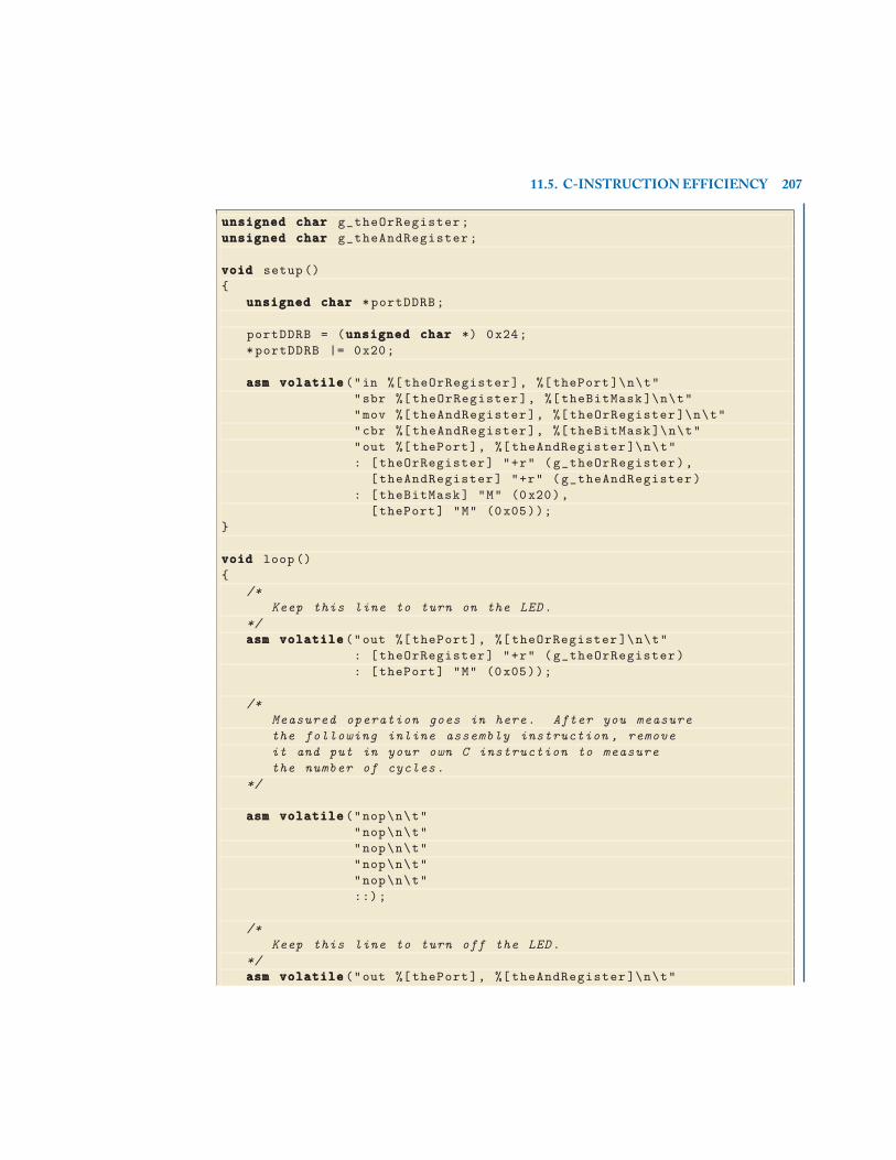
11.5. C-INSTRUCTION EFFICIENCY 207
unsignedunsignedunsigned charcharchar g_theOrRegister;unsignedunsignedunsigned charcharchar g_theAndRegister;
voidvoidvoid setup(){
unsignedunsignedunsigned charcharchar *portDDRB;
portDDRB = (unsignedunsignedunsigned charcharchar *) 0x24;*portDDRB |= 0x20;
asmasmasm volatilevolatilevolatile("in %[ theOrRegister], %[ thePort ]\n\t""sbr %[ theOrRegister], %[ theBitMask ]\n\t""mov %[ theAndRegister], %[ theOrRegister ]\n\t""cbr %[ theAndRegister], %[ theBitMask ]\n\t""out %[ thePort], %[ theAndRegister ]\n\t": [theOrRegister] "+r" (g_theOrRegister),
[theAndRegister] "+r" (g_theAndRegister): [theBitMask] "M" (0x20),
[thePort] "M" (0x05));}
voidvoidvoid loop(){
/*Keep this line to turn on the LED.
*/asmasmasm volatilevolatilevolatile("out %[ thePort], %[ theOrRegister ]\n\t"
: [theOrRegister] "+r" (g_theOrRegister): [thePort] "M" (0x05));
/*Measured operation goes in here. After you measurethe following inline assembly instruction , removeit and put in your own C instruction to measurethe number of cycles.
*/
asmasmasm volatilevolatilevolatile("nop\n\t""nop\n\t""nop\n\t""nop\n\t""nop\n\t"::);
/*Keep this line to turn off the LED.
*/asmasmasm volatilevolatilevolatile("out %[ thePort], %[ theAndRegister ]\n\t"
208 11. ASSEMBLY LANGUAGE
: [theAndRegister] "+r" (g_theAndRegister): [thePort] "M" (0x05));
delay (1000);}
Attach an oscilloscope to the LED output and measure the amount of time that the LED ishigh. Then remove the nop assembly instructions and re-measure the amount of time that theLED is high. Use the difference between the measurements as the time required to executethe five assembly nops. Take this measurement and the number of cycles required for the fivenops to determine the amount of time per cycle. You should be able to determine the numberof cycles by looking at the inline assembly instructions and comparing to the number of cyclesrequired in Apx. C.
11.6 From your measurements to problem 11.5, how fast do you calculate your processor clock tobe? How much time per cycle?
11.7 Modify the source code in problem 11.5 to measure the following (just remove the middleasm volatile instruction – you need to leave the first and third in order to get the LED toflash):
1. Cycles for an 8-bit addition/subtraction of two variables;
2. Cycles for an 8-bit multiplication of two variables (that is, two 8-bit numbers multipliedtogether to result in a 16-bit number);
3. Cycles for an 8-bit division of two variables;
4. Cycles for an 8-bit division of one variable by a constant power of 2;
5. Cycles for an 8-bit division of one variable by a constant value other than a power of 2;
6. Cycles for a 32-bit addition/subtraction of two variables;
7. Cycles for a 32-bit multiplication of two variables (that is, two 16-bit numbers multipliedtogether to result in a 32-bit number);
8. Cycles for a 32-bit division of two variables (that is, a 32-bit integer divided by someother integer);
9. Cycles for a 32-bit division of one variable by a constant power of 2;
10. Cycles for a 32-bit division of one variable by a constant value other than a power of 2;
11. Cycles for a floating point addition/subtraction of two variables;
12. Cycles for a floating point multiplication of two variables;
13. Cycles for a floating point division of two variables.
11.8 From your measurements to problem 11.7, state your estimations for number of cycles pereach high-level operation.

11.5. C-INSTRUCTION EFFICIENCY 209
11.9 From your measurements to problem 11.7, state the number of bytes for each program.
11.10 From your measurements to problem 11.7,what was the most expensive high-level instruction?
11.11 From your measurements to problem 11.7, was there a difference between the different integerdivisions? Explain.
11.12 From your measurements to problem 11.7, did you see a correlation between the number ofcycles and the number of bytes for each program? Explain.

211
C H A P T E R 12
Non-volatile Memory
12.1 INTRODUCTION
Many useful embedded systems require some kind of non-volatile memory for holding informationother than that of the code-space. Some of the most recent, common examples include smart phonesand portable music players. Smart phones such as Apple’s iPhone or Motorola’s Droid are digitalcell phones with the ability to run “apps” (short for applications). These apps are novel because theyare purchased and downloaded electronically, and then stored on the phone for subsequent usage.These programs have to be saved in non-volatile memory; otherwise, you would lose the programevery time you turned off the phone or ran out of battery life. Similarly, the portable music playerssuch as Apple’s iPod connect to a host computer in order to download music files that are storedon the portable device for subsequent listening. Again, the files need to be stored in non-volatilememory. Both of these example systems require a very large amount of non-volatile memory sinceapps and music are megabytes in size. It turns out that flash memory serves this purpose well. Infact, there are portable electronic devices being created with gigabytes of flash storage used as thephysical medium of the file systems for real-time operating systems such as Embedded Linux. TheRTOS is able to treat the flash memory as though it were a hard-disk such that it can store files,just like on your host computer.
This is all well and good for large-scale embedded systems with microprocessors, but youmight be wondering what good a lot of flash would do a microcontroller, which is generally resourcelimited in many ways. It turns out that many embedded systems have the need to store small piecesof data, on the order of kilobytes, in non-volatile memory, such that flash sizes are overkill. Theother primary non-volatile memory is the Electrically Erasable/Programmable Read Only Memory(EEPROM or E2 – pronounced “e-squared”), which is often manufactured in much smaller sizes(e.g., 8 KB to 32 KB). Then, embedded systems will connect an EEPROM to a microcontroller,usually via a serial bus, in order to save important operating parameters. As an example of the need,consider a cell phone in which you can adjust the backlight of the display, or the volume of thering-tone, or vibration mode. After you make such adjustments, the settings you choose are storedin an EEPROM. Consider if they weren’t, and you remove your battery. If they were not saved, allof your settings would have been lost.
12.1.1 EEPROM VIA C ON ATMEGA328PA very nice feature of the ATmega328P is the inclusion of an on-chip 1 KB EEPROM and anassociated peripheral interface used to read and write information from and to it. It turns out that
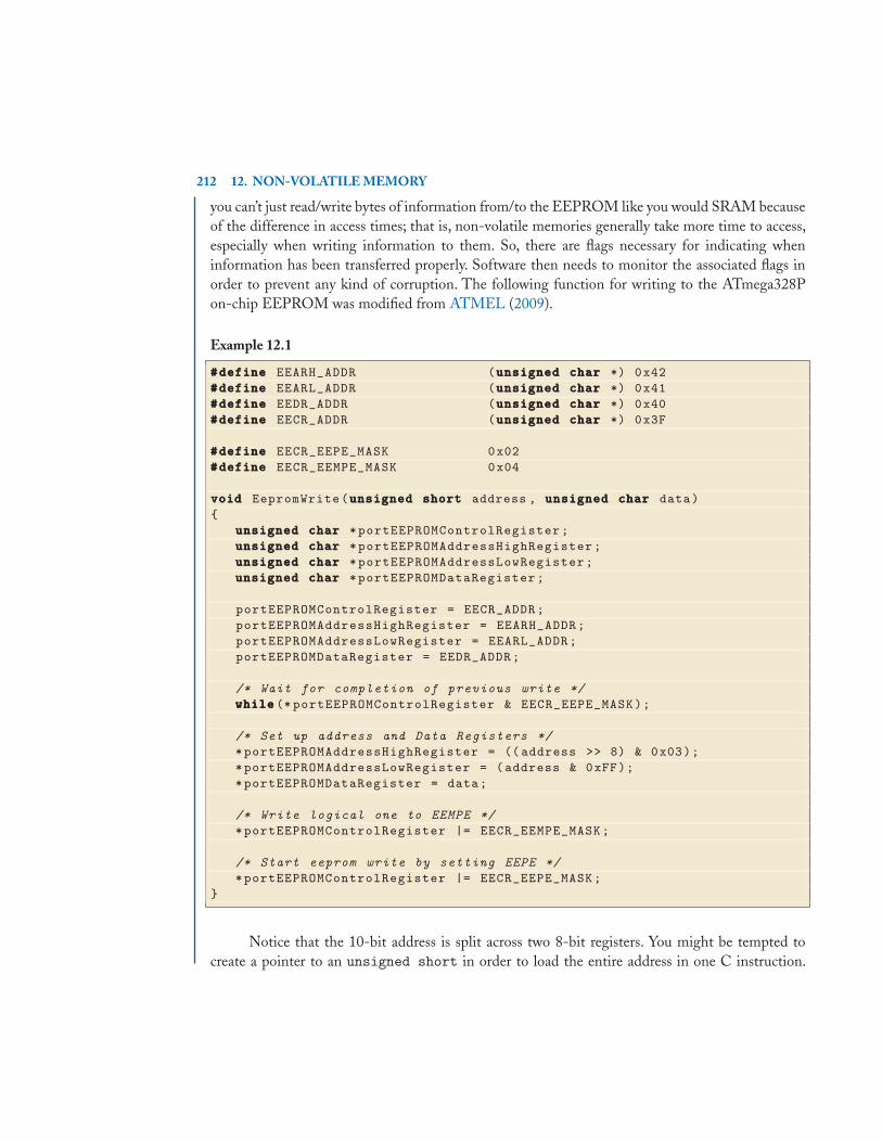
212 12. NON-VOLATILE MEMORY
you can’t just read/write bytes of information from/to the EEPROM like you would SRAM becauseof the difference in access times; that is, non-volatile memories generally take more time to access,especially when writing information to them. So, there are flags necessary for indicating wheninformation has been transferred properly. Software then needs to monitor the associated flags inorder to prevent any kind of corruption. The following function for writing to the ATmega328Pon-chip EEPROM was modified from ATMEL (2009).
Example 12.1
###definedefinedefine EEARH_ADDR (unsignedunsignedunsigned charcharchar *) 0x42###definedefinedefine EEARL_ADDR (unsignedunsignedunsigned charcharchar *) 0x41###definedefinedefine EEDR_ADDR (unsignedunsignedunsigned charcharchar *) 0x40###definedefinedefine EECR_ADDR (unsignedunsignedunsigned charcharchar *) 0x3F
###definedefinedefine EECR_EEPE_MASK 0x02###definedefinedefine EECR_EEMPE_MASK 0x04
voidvoidvoid EepromWrite(unsignedunsignedunsigned shortshortshort address , unsignedunsignedunsigned charcharchar data){
unsignedunsignedunsigned charcharchar *portEEPROMControlRegister;unsignedunsignedunsigned charcharchar *portEEPROMAddressHighRegister;unsignedunsignedunsigned charcharchar *portEEPROMAddressLowRegister;unsignedunsignedunsigned charcharchar *portEEPROMDataRegister;
portEEPROMControlRegister = EECR_ADDR;portEEPROMAddressHighRegister = EEARH_ADDR;portEEPROMAddressLowRegister = EEARL_ADDR;portEEPROMDataRegister = EEDR_ADDR;
/* Wait for completion of previous write */whilewhilewhile(* portEEPROMControlRegister & EECR_EEPE_MASK);
/* Set up address and Data Registers */*portEEPROMAddressHighRegister = (( address >> 8) & 0x03);*portEEPROMAddressLowRegister = (address & 0xFF);*portEEPROMDataRegister = data;
/* Write logical one to EEMPE */*portEEPROMControlRegister |= EECR_EEMPE_MASK;
/* Start eeprom write by setting EEPE */*portEEPROMControlRegister |= EECR_EEPE_MASK;
}
Notice that the 10-bit address is split across two 8-bit registers. You might be tempted tocreate a pointer to an unsigned short in order to load the entire address in one C instruction.
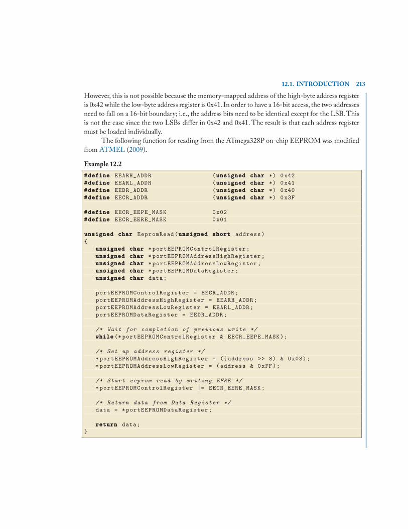
12.1. INTRODUCTION 213
However, this is not possible because the memory-mapped address of the high-byte address registeris 0x42 while the low-byte address register is 0x41. In order to have a 16-bit access, the two addressesneed to fall on a 16-bit boundary; i.e., the address bits need to be identical except for the LSB. Thisis not the case since the two LSBs differ in 0x42 and 0x41. The result is that each address registermust be loaded individually.
The following function for reading from the ATmega328P on-chip EEPROM was modifiedfrom ATMEL (2009).
Example 12.2
###definedefinedefine EEARH_ADDR (unsignedunsignedunsigned charcharchar *) 0x42###definedefinedefine EEARL_ADDR (unsignedunsignedunsigned charcharchar *) 0x41###definedefinedefine EEDR_ADDR (unsignedunsignedunsigned charcharchar *) 0x40###definedefinedefine EECR_ADDR (unsignedunsignedunsigned charcharchar *) 0x3F
###definedefinedefine EECR_EEPE_MASK 0x02###definedefinedefine EECR_EERE_MASK 0x01
unsignedunsignedunsigned charcharchar EepromRead(unsignedunsignedunsigned shortshortshort address){
unsignedunsignedunsigned charcharchar *portEEPROMControlRegister;unsignedunsignedunsigned charcharchar *portEEPROMAddressHighRegister;unsignedunsignedunsigned charcharchar *portEEPROMAddressLowRegister;unsignedunsignedunsigned charcharchar *portEEPROMDataRegister;unsignedunsignedunsigned charcharchar data;
portEEPROMControlRegister = EECR_ADDR;portEEPROMAddressHighRegister = EEARH_ADDR;portEEPROMAddressLowRegister = EEARL_ADDR;portEEPROMDataRegister = EEDR_ADDR;
/* Wait for completion of previous write */whilewhilewhile(* portEEPROMControlRegister & EECR_EEPE_MASK);
/* Set up address register */*portEEPROMAddressHighRegister = (( address >> 8) & 0x03);*portEEPROMAddressLowRegister = (address & 0xFF);
/* Start eeprom read by writing EERE */*portEEPROMControlRegister |= EECR_EERE_MASK;
/* Return data from Data Register */data = *portEEPROMDataRegister;
returnreturnreturn data;}
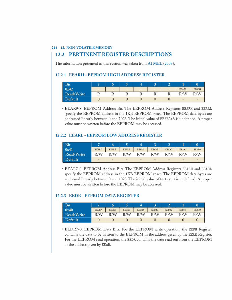
214 12. NON-VOLATILE MEMORY
12.2 PERTINENT REGISTER DESCRIPTIONS
The information presented in this section was taken from ATMEL (2009).
12.2.1 EEARH - EEPROM HIGH ADDRESS REGISTER
Bit 7 6 5 4 3 2 1 00x42 - - - - - - EEAR9 EEAR8
Read/Write R R R R R R R/W R/WDefault 0 0 0 0 0 0 - -
• EEAR9-8: EEPROM Address Bit. The EEPROM Address Registers EEARH and EEARLspecify the EEPROM address in the 1KB EEPROM space. The EEPROM data bytes areaddressed linearly between 0 and 1023. The initial value of EEAR9:8 is undefined. A propervalue must be written before the EEPROM may be accessed.
12.2.2 EEARL - EEPROM LOW ADDRESS REGISTER
Bit 7 6 5 4 3 2 1 00x41 EEAR7 EEAR6 EEAR5 EEAR4 EEAR3 EEAR2 EEAR1 EEAR0
Read/Write R/W R/W R/W R/W R/W R/W R/W R/WDefault - - - - - - - -
• EEAR7-0: EEPROM Address Bits. The EEPROM Address Registers EEARH and EEARLspecify the EEPROM address in the 1KB EEPROM space. The EEPROM data bytes areaddressed linearly between 0 and 1023. The initial value of EEAR7:0 is undefined. A propervalue must be written before the EEPROM may be accessed.
12.2.3 EEDR - EEPROM DATA REGISTER
Bit 7 6 5 4 3 2 1 00x40 EEDR7 EEDR6 EEDR5 EEDR4 EEDR3 EEDR2 EEDR1 EEDR0
Read/Write R/W R/W R/W R/W R/W R/W R/W R/WDefault 0 0 0 0 0 0 0 0
• EEDR7-0: EEPROM Data Bits. For the EEPROM write operation, the EEDR Registercontains the data to be written to the EEPROM in the address given by the EEAR Register.For the EEPROM read operation, the EEDR contains the data read out from the EEPROMat the address given by EEAR.

12.2. PERTINENT REGISTER DESCRIPTIONS 215
12.2.4 EECR - EEPROM CONTROL REGISTER
Bit 7 6 5 4 3 2 1 00x3F - - EEPM1 EEPM0 EERIE EEMPE EEPE EERE
Read/Write R R R/W R/W R/W R/W R/W R/WDefault 0 0 - - 0 0 - 0
• EEPM1-0: EEPROM Programming Mode Bits. The EEPROM Programming mode bitsetting defines which programming action that will be triggered when writing EEPE. It ispossible to program data in one atomic operation (erase the old value and program the newvalue) or to split the Erase and Write operations in two different operations.The programmingtimes for the different modes are shown in Table 12.1. While EEPE is set, any write to EEPMxwill be ignored. During reset, the EEPMx bits will be reset to 00 unless the EEPROM is busyprogramming.
Table 12.1: EEPROM Mode BitsEEPM1-0 Programming Time Operation
00 3.4 msec Erase and Write in one atomic operation01 1.8 msec Erase only10 1.8 msec Write only11 - Reserved
• EEMPE: EEPROM Master Write Enable. The EEMPE bit determines whether setting EEPEto one causes the EEPROM to be written. When EEMPE is set, setting EEPE within four clockcycles will write data to the EEPROM at the selected address. If EEMPE is zero, setting EEPEwill have no effect. When EEMPE has been written to one by software, hardware clears the bitto zero after four clock cycles.
• EEPE: EEPROM Write Enable.The EEPROM Write Enable Signal EEPE is the write strobeto the EEPROM. When address and data are correctly set up, the EEPE bit must be writtento one to write the value into the EEPROM. The EEMPE bit must be written to one beforea logical one is written to EEPE; otherwise, no EEPROM write takes place. The procedurelisted in Ex. 12.1 should be followed when writing the EEPROM.
• EERE: EEPROM Read Enable. The EEPROM Read Enable Signal EERE is the read strobeto the EEPROM. When the correct address is set up in the EEAR Register, the EERE bit mustbe written to a logic one to trigger the EEPROM read. The EEPROM read access takes oneinstruction, and the requested data is available immediately. When the EEPROM is read, theCPU is halted for four cycles before the next instruction is executed.
The user should poll the EEPE bit before starting the read operation. If a write operation is inprogress, it is neither possible to read the EEPROM nor to change the EEAR Register.

216 12. NON-VOLATILE MEMORY
The procedure listed in Ex. 12.2 should be followed when reading from the EEPROM.
• See Ch. 9 for interrupt-related bit descriptions.
PROBLEMS12.1 Pick an address in the EEPROM (i.e., addr ∈ {0, ..., 1023}) to hold a special byte of data
used to indicate the presence of stored data. Create a program that writes a special byte (e.g.,0xAA) to the EEPROM.
12.2 Create a program that clears the byte stored at the address in problem 12.1. That is, write0x00 to the location.
12.3 Create a program that reads the byte stored at the address in problem 12.1. If the byte is equalto the special byte used in problem 12.1, then read out the stored value for use as the initialvalue in the rest of the program. If the byte is not equal to the special value, use a pre-definedconstant value as the initial value in the rest of the program.
For the rest of the program, given the initial value between 0 and 9, repeatedly output thedigits ‘0’ through ‘9’ on a seven-segment display with a one-second interval between each digit.After each digit is displayed, save the current digit to a location in the EEPROM, and be sureto write the special byte to the address determined in problem 12.1.
Verify that when you reset the board, the value is read out of the EEPROM and continuescounting from where it left off.
12.4 Use the program from problem 12.2 to clear the EEPROM.Verify that the program in problem12.3 starts at the default value after the EEPROM is cleared.
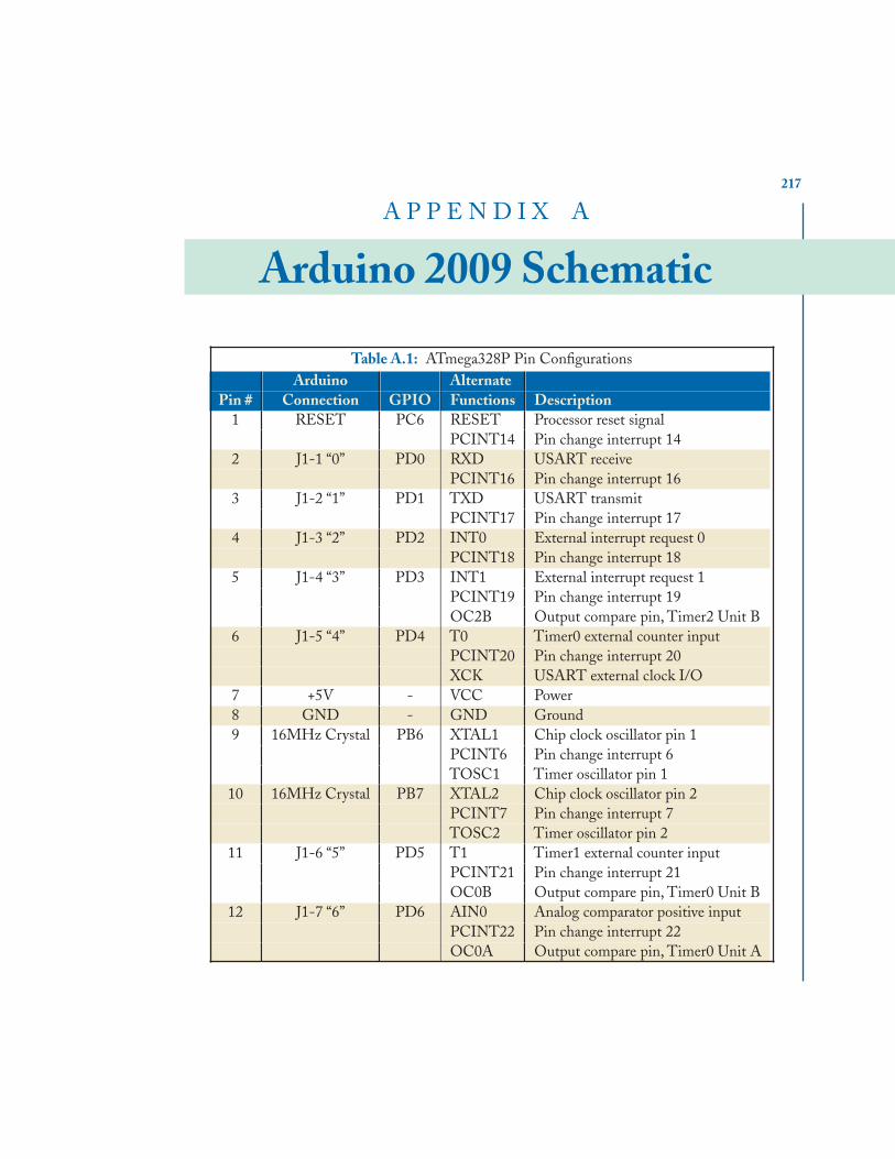
217
A P P E N D I X A
Arduino 2009 Schematic
Table A.1: ATmega328P Pin ConfigurationsArduino Alternate
Pin # Connection GPIO Functions Description1 RESET PC6 RESET Processor reset signal
PCINT14 Pin change interrupt 142 J1-1 “0” PD0 RXD USART receive
PCINT16 Pin change interrupt 163 J1-2 “1” PD1 TXD USART transmit
PCINT17 Pin change interrupt 174 J1-3 “2” PD2 INT0 External interrupt request 0
PCINT18 Pin change interrupt 185 J1-4 “3” PD3 INT1 External interrupt request 1
PCINT19 Pin change interrupt 19OC2B Output compare pin, Timer2 Unit B
6 J1-5 “4” PD4 T0 Timer0 external counter inputPCINT20 Pin change interrupt 20XCK USART external clock I/O
7 +5V - VCC Power8 GND - GND Ground9 16MHz Crystal PB6 XTAL1 Chip clock oscillator pin 1
PCINT6 Pin change interrupt 6TOSC1 Timer oscillator pin 1
10 16MHz Crystal PB7 XTAL2 Chip clock oscillator pin 2PCINT7 Pin change interrupt 7TOSC2 Timer oscillator pin 2
11 J1-6 “5” PD5 T1 Timer1 external counter inputPCINT21 Pin change interrupt 21OC0B Output compare pin, Timer0 Unit B
12 J1-7 “6” PD6 AIN0 Analog comparator positive inputPCINT22 Pin change interrupt 22OC0A Output compare pin, Timer0 Unit A

218 A. ARDUINO 2009 SCHEMATIC
Table A.1: ATmega328P Pin ConfigurationsArduino Alternate
Pin # Connection GPIO Functions Description13 J1-8 “7” PD7 AIN1 Analog comparator negative input
PCINT23 Pin change interrupt 2314 J3-1 “8” PB0 ICP1 Timer1 input capture input
PCINT0 Pin change interrupt 0CLKO Divided system clock output
15 J3-2 “9” PB1 OC1A Output compare pin, Timer1 Unit APCINT1 Pin change interrupt 1
16 J3-3 “10” PB2 OC1B Output compare pin, Timer1 Unit BPCINT2 Pin change interrupt 2SS SPI slave select
17 J3-4 “11” PB3 OC2A Output compare pin, Timer2 Unit APCINT3 Pin change interrupt 3MOSI SPI master-out/slave-in
18 J3-5 “12” PB4 PCINT4 Pin change interrupt 4MISO SPI master-in/slave-out
19 J3-6 “13” PB5 PCINT5 Pin change interrupt 5SCK SPI clock input
20 +5V - AVCC Analog supply voltage for ADC21 J3-8 “AREF” - AREF External ADC reference voltage22 GND - GND Ground23 J2-1 “0” PC0 ADC0 ADC input channel 0
PCINT8 Pin change interrupt 824 J2-2 “1” PC1 ADC1 ADC input channel 1
PCINT9 Pin change interrupt 925 J2-3 “2” PC2 ADC2 ADC input channel 2
PCINT10 Pin change interrupt 1026 J2-4 “3” PC3 ADC3 ADC input channel 3
PCINT11 Pin change interrupt 1127 J2-5 “4” PC4 ADC4 ADC input channel 4
PCINT12 Pin change interrupt 12SDA TWI serial data
28 J2-6 “5” PC5 ADC5 ADC input channel 5PCINT13 Pin change interrupt 13SCL TWI serial clock

219
Figure
A.1:
Arduino
Duem
ilanove(“2009”)schem
atic.Source:A
rduino,http://www.arduino.cc
©2009
Arduino.D
istributableundera
Creative
Com
mons
Attribution-ShareA
like3.0
License,h
ttp://
creativecommons.org/licenses/by-sa/3.0/.


221
A P P E N D I X B
ATmega328P Registers
B.1 REGISTER SUMMARY
Table B.1: Memory Mapped Register SummaryBit
Addr Name 7 6 5 4 3 2 1 00x00-1F R0-R31 CPU General Purpose Working Registers mapped to data space
0x20-22 Reserved - - - - - - - -
0x23 PINB PINB7 PINB6 PINB5 PINB4 PINB3 PINB2 PINB1 PINB0
0x24 DDRB DDRB7 DDRB6 DDRB5 DDRB4 DDRB3 DDRB2 DDRB1 DDRB0
0x25 PORTB PORTB7 PORTB6 PORTB5 PORTB4 PORTB3 PORTB2 PORTB1 PORTB0
0x26 PINC - PINC6 PINC5 PINC4 PINC3 PINC2 PINC1 PINC0
0x27 DDRC - DDRC6 DDRC5 DDRC4 DDRC3 DDRC2 DDRC1 DDRC0
0x28 PORTC - PORTC6 PORTC5 PORTC4 PORTC3 PORTC2 PORTC1 PORTC0
0x29 PIND PIND7 PIND6 PIND5 PIND4 PIND3 PIND2 PIND1 PIND0
0x2A DDRD DDRD7 DDRD6 DDRD5 DDRD4 DDRD3 DDRD2 DDRD1 DDRD0
0x2B PORTD PORTD7 PORTD6 PORTD5 PORTD4 PORTD3 PORTD2 PORTD1 PORTD0
0x2C-34 Reserved - - - - - - - -
0x35 TIFR0 - - - - - OCF0B OCF0A TOV0
0x36 TIFR1 - - ICF1 - - OCF1B OCF1A TOV1
0x37 TIFR2 - - - - - OCF2B OCF2A TOV2
0x38-3A Reserved - - - - - - - -
0x3B PCIFR - - - - - PCIF2 PCIF1 PCIF0
0x3C EIFR - - - - - - INTF1 INTF0
0x3D EIMSK - - - - - - INT1 INT0
0x3E GPIOR0 General Purpose I/O Register 0
0x3F EECR - - EEPM1 EEPM0 EERIE EEMPE EEPE EERE
0x40 EEDR EEPROM Data Register
0x41 EEARL EEPROM Address Register Low Byte
0x42 EEARH EEPROM Address Register High Byte
0x43 GTCCR TSM - - - - - PSRASY PSRSYN
0x44 TCCR0A COM0A1 COM0A0 COM0B1 COM0B0 - - WGM01 WGM00
0x45 TCCR0B FOC0A FOC0B - - WGM02 CS02 CS01 CS00

222 B. ATMEGA328P REGISTERS
Table B.1: Memory Mapped Register SummaryBit
Addr Name 7 6 5 4 3 2 1 00x46 TCNT0 Timer/Counter0
0x47 OCR0A Timer/Counter0 Output Compare Register A
0x48 OCR0B Timer/Counter0 Output Compare Register B
0x49 Reserved - - - - - - - -
0x4A GPIOR1 General Purpose I/O Register 1
0x4B GPIOR2 General Purpose I/O Register 2
0x4C SPCR SPIE SPE DORD MSTR CPOL CPHA SPR1 SPR0
0x4D SPSR SPIF WCOL - - - - - SPI2X
0x4E SPDR SPI Data Register
0x4F Reserved - - - - - - - -
0x50 ACSR ACD ACBG ACO ACI ACIE ACIC ACIS1 ACIS0
0x51-52 Reserved - - - - - - - -
0x53 SMCR - - - - SM2 SM1 SM0 SE
0x54 MCUSR - - - - WDRF BORF EXTRF PORF
0x55 MCUCR - BODS BODSE PUD - - IVSEL IVCE
0x56 Reserved - - - - - - - -
0x57 SPMCSR SPMIE RWWSB - RWWSRE BLBSET PGWRT PGERS SLFPRG
0x58-5C Reserved - - - - - - - -
0x5D SPL SP7 SP6 SP5 SP4 SP3 SP2 SP1 SP0
0x5E SPH - - - - - SP10 SP9 SP8
0x5F SREG I T H S V N Z C
0x60 WDTCSR WDIF WDIE WDP3 WDCE WDE WDP2 WDP1 WDP0
0x61 CLKPR CLKPCE - - - CLKPS3 CLKPS2 CLKPS1 CLKPS0
0x62-63 Reserved - - - - - - - -
0x64 PRR PRTWI PRTIM2 PRTIM0 - PRTIM1 PRSPI PRUSART0 PRADC
0x65 Reserved - - - - - - - -
0x66 OSCCAL Oscillator Calibration Register
0x67 Reserved - - - - - - - -
0x68 PCICR - - - - - PCIE2 PCIE1 PCIE0
0x69 EICRA - - - - ISC11 ISC10 ISC01 ISC00
0x6A Reserved - - - - - - - -
0x6B PCMSK0 PCINT7 PCINT6 PCINT5 PCINT4 PCINT3 PCINT2 PCINT1 PCINT0
0x6C PCMSK1 - PCINT14 PCINT13 PCINT12 PCINT11 PCINT10 PCINT9 PCINT8
0x6D PCMSK2 PCINT23 PCINT22 PCINT21 PCINT20 PCINT19 PCINT18 PCINT17 PCINT16
0x6E TIMSK0 - - - - - OCIE0B OCIE0A TOIE0
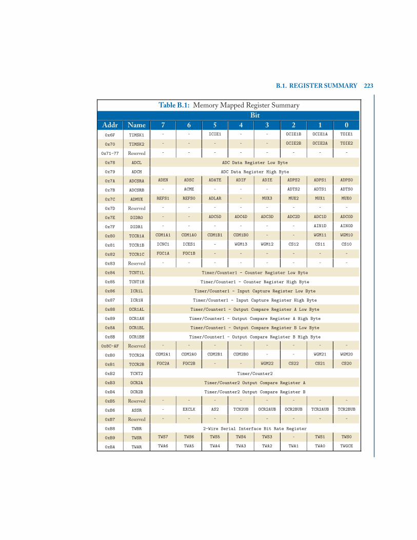
B.1. REGISTER SUMMARY 223
Table B.1: Memory Mapped Register SummaryBit
Addr Name 7 6 5 4 3 2 1 00x6F TIMSK1 - - ICIE1 - - OCIE1B OCIE1A TOIE1
0x70 TIMSK2 - - - - - OCIE2B OCIE2A TOIE2
0x71-77 Reserved - - - - - - - -
0x78 ADCL ADC Data Register Low Byte
0x79 ADCH ADC Data Register High Byte
0x7A ADCSRA ADEN ADSC ADATE ADIF ADIE ADPS2 ADPS1 ADPS0
0x7B ADCSRB - ACME - - - ADTS2 ADTS1 ADTS0
0x7C ADMUX REFS1 REFS0 ADLAR - MUX3 MUX2 MUX1 MUX0
0x7D Reserved - - - - - - - -
0x7E DIDR0 - - ADC5D ADC4D ADC3D ADC2D ADC1D ADC0D
0x7F DIDR1 - - - - - - AIN1D AIN0D
0x80 TCCR1A COM1A1 COM1A0 COM1B1 COM1B0 - - WGM11 WGM10
0x81 TCCR1B ICNC1 ICES1 - WGM13 WGM12 CS12 CS11 CS10
0x82 TCCR1C FOC1A FOC1B - - - - - -
0x83 Reserved - - - - - - - -
0x84 TCNT1L Timer/Counter1 - Counter Register Low Byte
0x85 TCNT1H Timer/Counter1 - Counter Register High Byte
0x86 ICR1L Timer/Counter1 - Input Capture Register Low Byte
0x87 ICR1H Timer/Counter1 - Input Capture Register High Byte
0x88 OCR1AL Timer/Counter1 - Output Compare Register A Low Byte
0x89 OCR1AH Timer/Counter1 - Output Compare Register A High Byte
0x8A OCR1BL Timer/Counter1 - Output Compare Register B Low Byte
0x8B OCR1BH Timer/Counter1 - Output Compare Register B High Byte
0x8C-AF Reserved - - - - - - - -
0xB0 TCCR2A COM2A1 COM2A0 COM2B1 COM2B0 - - WGM21 WGM20
0xB1 TCCR2B FOC2A FOC2B - - WGM22 CS22 CS21 CS20
0xB2 TCNT2 Timer/Counter2
0xB3 OCR2A Timer/Counter2 Output Compare Register A
0xB4 OCR2B Timer/Counter2 Output Compare Register B
0xB5 Reserved - - - - - - - -
0xB6 ASSR - EXCLK AS2 TCN2UB OCR2AUB OCR2BUB TCR2AUB TCR2BUB
0xB7 Reserved - - - - - - - -
0xB8 TWBR 2-Wire Serial Interface Bit Rate Register
0xB9 TWSR TWS7 TWS6 TWS5 TWS4 TWS3 - TWS1 TWS0
0xBA TWAR TWA6 TWA5 TWA4 TWA3 TWA2 TWA1 TWA0 TWGCE
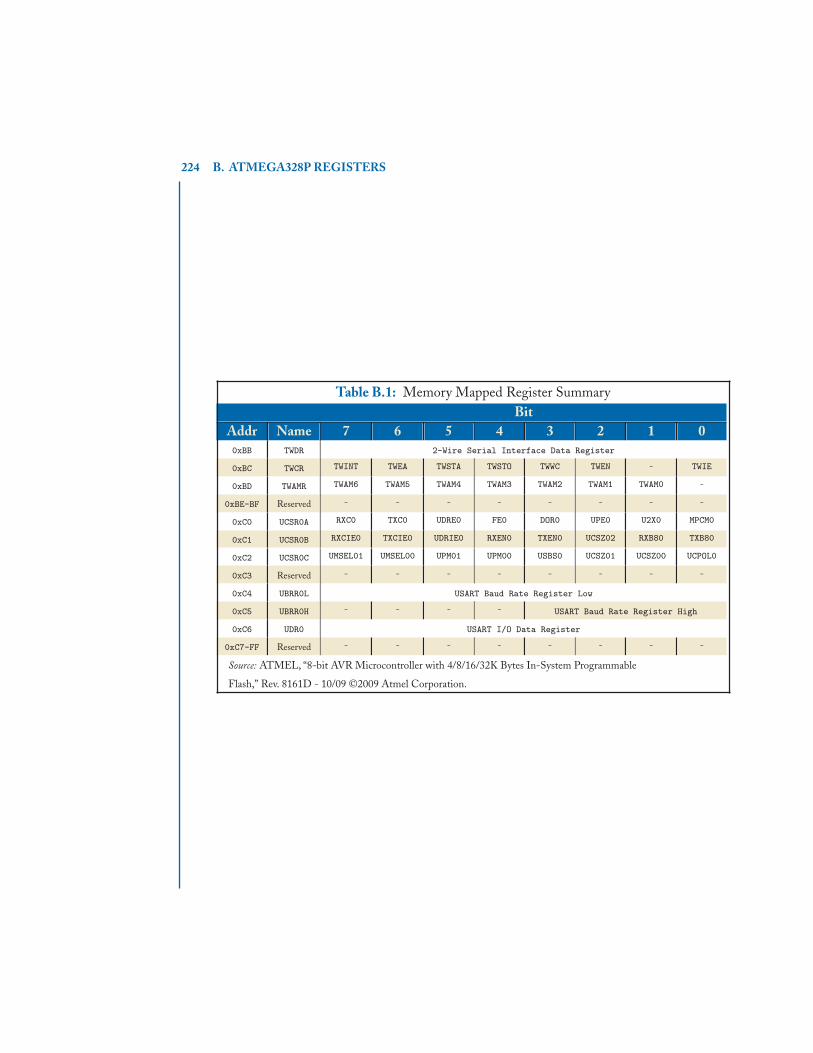
224 B. ATMEGA328P REGISTERS
Table B.1: Memory Mapped Register SummaryBit
Addr Name 7 6 5 4 3 2 1 00xBB TWDR 2-Wire Serial Interface Data Register
0xBC TWCR TWINT TWEA TWSTA TWSTO TWWC TWEN - TWIE
0xBD TWAMR TWAM6 TWAM5 TWAM4 TWAM3 TWAM2 TWAM1 TWAM0 -
0xBE-BF Reserved - - - - - - - -
0xC0 UCSR0A RXC0 TXC0 UDRE0 FE0 DOR0 UPE0 U2X0 MPCM0
0xC1 UCSR0B RXCIE0 TXCIE0 UDRIE0 RXEN0 TXEN0 UCSZ02 RXB80 TXB80
0xC2 UCSR0C UMSEL01 UMSEL00 UPM01 UPM00 USBS0 UCSZ01 UCSZ00 UCPOL0
0xC3 Reserved - - - - - - - -
0xC4 UBRR0L USART Baud Rate Register Low
0xC5 UBRR0H - - - - USART Baud Rate Register High
0xC6 UDR0 USART I/O Data Register
0xC7-FF Reserved - - - - - - - -
Source: ATMEL, “8-bit AVR Microcontroller with 4/8/16/32K Bytes In-System Programmable
Flash,” Rev. 8161D - 10/09 ©2009 Atmel Corporation.

225
A P P E N D I X C
ATmega328P AssemblyInstructions
C.1 INSTRUCTION SET SUMMARY
Table C.1: Arithmetic InstructionsAffected Clk
Mnemonic Description Operation SREG Bits Cyc
ADD Rd,Rr Add two registers Rd ← Rd + Rr -,-,H,-,V,N,Z,C 1
ADC Rd,Rr Add with carry two registers Rd ← Rd + Rr +SREG[C] -,-,H,-,V,N,Z,C 1
ADIW Rdl,K Add immediate to word Rdh:Rdl ←Rdh:Rdl + K -,-,-,S,V,N,Z,C 2
SUB Rd,Rr Subtract two registers Rd ← Rd - Rr -,-,H,-,V,N,Z,C 1
SUBI Rd,K Subtract constant from register Rd ← Rd - K -,-,H,-,V,N,Z,C 1
SBC Rd,Rr Subtract with carry two registers Rd ← Rd - Rr -SREG[C] -,-,H,-,V,N,Z,C 1
SBCI Rd,K Subtract with carry immediate from reg. Rd ← Rd - K -SREG[C] -,-,H,-,V,N,Z,C 1
SBIW Rdl,K Subtract immediate from word Rdh:Rdl ←Rdh:Rdl - K -,-,-,S,V,N,Z,C 2
NEG Rd Two’s complement negation register Rd ← 0x00 - Rd -,-,H,-,V,N,Z,C 1
INC Rd Increment register Rd ← Rd + 1 -,-,-,-,V,N,Z,- 1
DEC Rd Decrement register Rd ← Rd - 1 -,-,-,-,V,N,Z,- 1
TST Rd Test register for zero of minus Rd ← Rd ∩ Rd -,-,-,-,V,N,Z,- 1
MUL Rd,Rr Multiply unsigned two registers R1:R0 ←Rd × Rr -,-,-,-,-,-,Z,C 2
MULS Rd,Rr Multiply signed two registers R1:R0 ←Rd × Rr -,-,-,-,-,-,Z,C 2
MULSU Rd,Rr Multiply signed with unsigned registers R1:R0 ←Rd × Rr -,-,-,-,-,-,Z,C 2
FMUL Rd,Rr Fractional multiply unsigned two registers R1:R0 ←(Rd × Rr) � 1 -,-,-,-,-,-,Z,C 2
FMULS Rd,Rr Frac. mult. signed two registers R1:R0 ←(Rd × Rr) � 1 -,-,-,-,-,-,Z,C 2
FMULSU Rd,Rr Frac. mult. signed with unsigned registers R1:R0 ←(Rd × Rr) � 1 -,-,-,-,-,-,Z,C 2
Source: ATMEL, “8-bit AVR Microcontroller with 4/8/16/32K Bytes In-System Programmable
Flash,” Rev. 8161D - 10/09 ©2009 Atmel Corporation.

226 C. ATMEGA328P ASSEMBLY INSTRUCTIONS
Table C.2: Logic InstructionsAffected Clk
Mnemonic Description Operation SREG Bits Cyc
AND Rd,Rr Logical AND two registers Rd ← Rd ∩ Rr -,-,-,-,V,N,Z,- 1
ANDI Rd,K Logical AND immediate and register Rd ← Rd ∩ K -,-,-,-,V,N,Z,- 1
OR Rd,Rr Logical OR two registers Rd ← Rd ∪ Rr -,-,-,-,V,N,Z,- 1
ORI Rd,K Logical OR constant and register Rd ← Rd ∪ K -,-,-,-,V,N,Z,- 1
EOR Rd,Rr Exclusive OR two registers Rd ← Rd ⊕ Rr -,-,-,-,V,N,Z,- 1
COM Rd One’s complement negation register Rd ← 0xFF - Rd -,-,-,-,V,N,Z,C 1
SBR Rd,K Set bit(s) in register Rd ← Rd ∪ K -,-,-,-,V,N,Z,- 1
CBR Rd,K Clear bit(s) in register Rd ← Rd ∩ (0xFF - K) -,-,-,-,V,N,Z,- 1
CLR Rd Clear register Rd ← Rd ⊕ Rd -,-,-,-,V,N,Z,- 1
SER Rd Set register Rd ← 0xFF -,-,-,-,-,-,-,- 1
Source: ATMEL, “8-bit AVR Microcontroller with 4/8/16/32K Bytes In-System Programmable
Flash,” Rev. 8161D - 10/09 ©2009 Atmel Corporation.
Table C.3: Branch InstructionsAffected Clk
Mnemonic Description Operation SREG Bits Cyc
RJMP k Relative jump PC ← PC + k + 1 -,-,-,-,-,-,-,- 2
IJMP Indirect jump to (Z) PC ← Z -,-,-,-,-,-,-,- 2
JMP k Direct jump PC ← k -,-,-,-,-,-,-,- 3
RCALL k Relative subroutine call (SP) ← PC + S -,-,-,-,-,-,-,- 3
SP ← SP - 2
PC ← PC + k + 1
ICALL Indirect call to (Z) (SP) ← PC + S -,-,-,-,-,-,-,- 3
SP ← SP - 2
PC ← Z
CALL k Direct subroutine call (SP) ← PC + S -,-,-,-,-,-,-,- 4
SP ← SP - 2
PC ← k
RET Subroutine return SP ← SP + 2 -,-,-,-,-,-,-,- 4
PC ← (SP)
RETI Interrupt subroutine return SP ← SP + 2 I,-,-,-,-,-,-,- 4
PC ← (SP)
CPSE Rd,Rr Compare, skip if equal PC ← PC + 1 -,-,-,-,-,-,-,- 1,2
if (Rd=Rr)then or 3
PC ← PC + N

C.1. INSTRUCTION SET SUMMARY 227
Table C.3: Branch InstructionsAffected Clk
Mnemonic Description Operation SREG Bits Cyc
CP Rd,Rr Compare two registers Rd - Rr -,-,H,-,V,N,Z,C 1
CPC Rd,Rr Compare with carry two registers Rd - Rr - SREG[C] -,-,H,-,V,N,Z,C 1
CPI Rd,K Compare immediate and register Rd - K -,-,H,-,V,N,Z,C 1
SBRC Rr,b Skip if bit in register cleared PC ← PC + 1 -,-,-,-,-,-,-,- 1,2
if (Rr[b]=0)then or 3
PC ← PC + N
SBRS Rr,b Skip if bit in register set PC ← PC + 1 -,-,-,-,-,-,-,- 1,2
if (Rr[b]=1)then or 3
PC ← PC + N
SBIC P,b Skip if bit in I/O register cleared PC ← PC + 1 -,-,-,-,-,-,-,- 1,2
if (P[b]=0)then or 3
PC ← PC + N
SBIS P,b Skip if bit in I/O register set PC ← PC + 1 -,-,-,-,-,-,-,- 1,2
if (P[b]=1)then or 3
PC ← PC + N
BRBC b,k Branch if status bit cleared PC ← PC + 1 -,-,-,-,-,-,-,- 1,2
if (SREG[b]=0)then
PC ← PC + k
BRBS b,k Branch if status bit set PC ← PC + 1 -,-,-,-,-,-,-,- 1,2
if (SREG[b]=1)then
PC ← PC + k
BRNE k Branch if not equal PC ← PC + 1 -,-,-,-,-,-,-,- 1,2
if (SREG[Z]=0)then
PC ← PC + k
BREQ k Branch if equal PC ← PC + 1 -,-,-,-,-,-,-,- 1,2
if (SREG[Z]=1)then
PC ← PC + k
BRCC k Branch if carry cleared PC ← PC + 1 -,-,-,-,-,-,-,- 1,2
if (SREG[C]=0)then
PC ← PC + k
BRCS k Branch if carry set PC ← PC + 1 -,-,-,-,-,-,-,- 1,2
if (SREG[C]=1)then
PC ← PC + k
BRSH k Branch if same or higher PC ← PC + 1 -,-,-,-,-,-,-,- 1,2
if (SREG[C]=0)then
PC ← PC + k
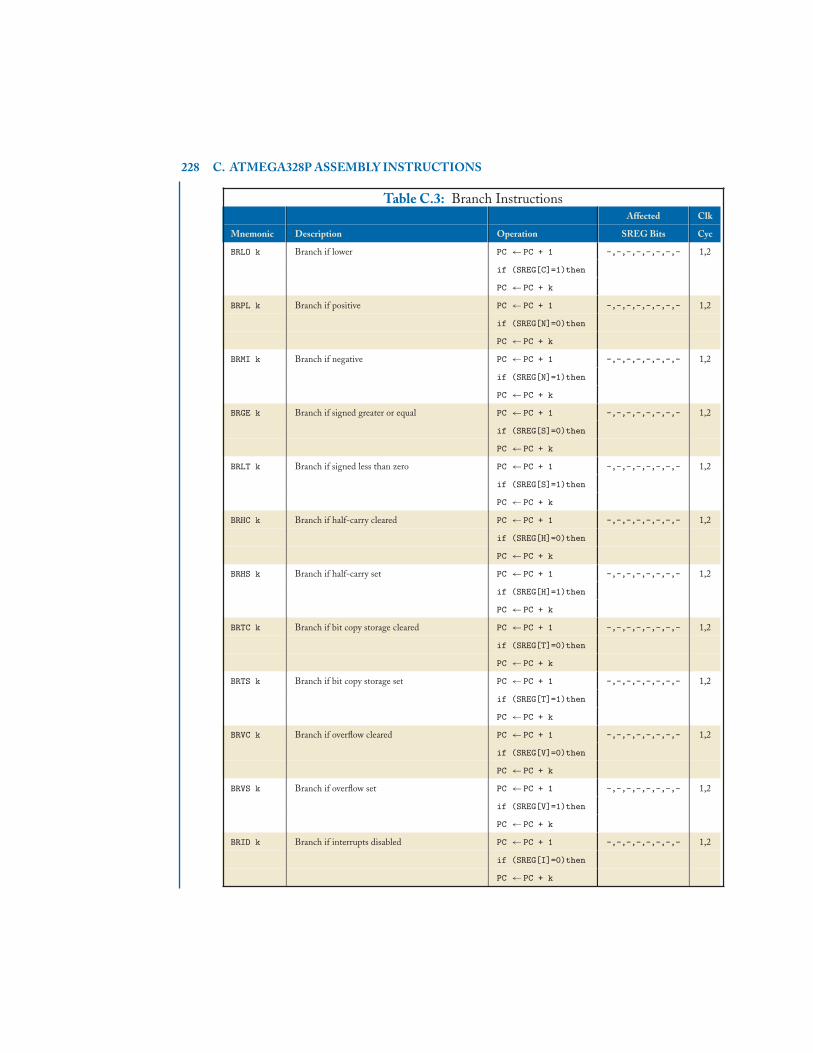
228 C. ATMEGA328P ASSEMBLY INSTRUCTIONS
Table C.3: Branch InstructionsAffected Clk
Mnemonic Description Operation SREG Bits Cyc
BRLO k Branch if lower PC ← PC + 1 -,-,-,-,-,-,-,- 1,2
if (SREG[C]=1)then
PC ← PC + k
BRPL k Branch if positive PC ← PC + 1 -,-,-,-,-,-,-,- 1,2
if (SREG[N]=0)then
PC ← PC + k
BRMI k Branch if negative PC ← PC + 1 -,-,-,-,-,-,-,- 1,2
if (SREG[N]=1)then
PC ← PC + k
BRGE k Branch if signed greater or equal PC ← PC + 1 -,-,-,-,-,-,-,- 1,2
if (SREG[S]=0)then
PC ← PC + k
BRLT k Branch if signed less than zero PC ← PC + 1 -,-,-,-,-,-,-,- 1,2
if (SREG[S]=1)then
PC ← PC + k
BRHC k Branch if half-carry cleared PC ← PC + 1 -,-,-,-,-,-,-,- 1,2
if (SREG[H]=0)then
PC ← PC + k
BRHS k Branch if half-carry set PC ← PC + 1 -,-,-,-,-,-,-,- 1,2
if (SREG[H]=1)then
PC ← PC + k
BRTC k Branch if bit copy storage cleared PC ← PC + 1 -,-,-,-,-,-,-,- 1,2
if (SREG[T]=0)then
PC ← PC + k
BRTS k Branch if bit copy storage set PC ← PC + 1 -,-,-,-,-,-,-,- 1,2
if (SREG[T]=1)then
PC ← PC + k
BRVC k Branch if overflow cleared PC ← PC + 1 -,-,-,-,-,-,-,- 1,2
if (SREG[V]=0)then
PC ← PC + k
BRVS k Branch if overflow set PC ← PC + 1 -,-,-,-,-,-,-,- 1,2
if (SREG[V]=1)then
PC ← PC + k
BRID k Branch if interrupts disabled PC ← PC + 1 -,-,-,-,-,-,-,- 1,2
if (SREG[I]=0)then
PC ← PC + k
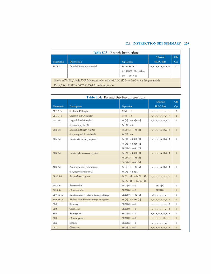
C.1. INSTRUCTION SET SUMMARY 229
Table C.3: Branch InstructionsAffected Clk
Mnemonic Description Operation SREG Bits Cyc
BRIE k Branch if interrupts enabled PC ← PC + 1 -,-,-,-,-,-,-,- 1,2
if (SREG[I]=1)then
PC ← PC + k
Source: ATMEL, “8-bit AVR Microcontroller with 4/8/16/32K Bytes In-System Programmable
Flash,” Rev. 8161D - 10/09 ©2009 Atmel Corporation.
Table C.4: Bit and Bit-Test InstructionsAffected Clk
Mnemonic Description Operation SREG Bits Cyc
SBI P,b Set bit in I/O register P[b] ←1 -,-,-,-,-,-,-,- 2
CBI P,b Clear bit in I/O register P[b] ←0 -,-,-,-,-,-,-,- 2
LSL Rd Logical shift left register Rd[n] ←Rd[n-1] -,-,-,-,V,N,Z,C 1
(i.e., multiply-by-2) Rd[0] ←0
LSR Rd Logical shift right register Rd[n-1] ←Rd[n] -,-,-,-,V,N,Z,C 1
(i.e., unsigned divide-by-2) Rd[7] ←0
ROL Rd Rotate left via carry register Rd[0] ←SREG[C] -,-,-,-,V,N,Z,C 1
Rd[n] ←Rd[n-1]
SREG[C] ←Rd[7]
ROR Rd Rotate right via carry register Rd[7] ←SREG[C] -,-,-,-,V,N,Z,C 1
Rd[n-1] ←Rd[n]
SREG[C] ←Rd[0]
ASR Rd Arithmetic shift right register Rd[n-1] ←Rd[n] -,-,-,-,V,N,Z,C 1
(i.e., signed divide-by-2) Rd[7] ←Rd[7]
SWAP Rd Swap nibbles register Rd[3..0] ←Rd[7..4] -,-,-,-,-,-,-,- 1
Rd[7..4] ←Rd[3..0]
BSET b Set status bit SREG[b] ←1 SREG[b] 1
BCLR b Clear status bit SREG[b] ←0 SREG[b] 1
BST Rr,b Bit store from register to bit copy storage SREG[T] ←Rr[b] -,T,-,-,-,-,-,- 1
BLD Rd,b Bit load from bit copy storage to register Rd[b] ←SREG[T] -,-,-,-,-,-,-,- 1
SEC Set carry SREG[C] ←1 -,-,-,-,-,-,-,C 1
CLC Clear carry SREG[C] ←0 -,-,-,-,-,-,-,C 1
SEN Set negative SREG[N] ←1 -,-,-,-,-,N,-,- 1
CLN Clear negative SREG[N] ←0 -,-,-,-,-,N,-,- 1
SEZ Set zero SREG[Z] ←1 -,-,-,-,-,-,Z,- 1
CLZ Clear zero SREG[Z] ←0 -,-,-,-,-,-,Z,- 1

230 C. ATMEGA328P ASSEMBLY INSTRUCTIONS
Table C.4: Bit and Bit-Test InstructionsAffected Clk
Mnemonic Description Operation SREG Bits Cyc
SEI Global interrupts enabled SREG[I] ←1 I,-,-,-,-,-,-,- 1
CLI Global interrupts disabled SREG[I] ←0 I,-,-,-,-,-,-,- 1
SES Set signed SREG[S] ←1 -,-,-,S,-,-,-,- 1
CLS Clear signed SREG[S] ←0 -,-,-,S,-,-,-,- 1
SEV Set overflow SREG[V] ←1 -,-,-,-,V,-,-,- 1
CLV Clear overflow SREG[V] ←0 -,-,-,-,V,-,-,- 1
SET Set bit copy storage SREG[T] ←1 -,T,-,-,-,-,-,- 1
CLT Clear bit copy storage SREG[T] ←0 -,T,-,-,-,-,-,- 1
SEH Set half-carry SREG[H] ←1 -,-,H,-,-,-,-,- 1
CLH Clear half-carry SREG[H] ←0 -,-,H,-,-,-,-,- 1
Source: ATMEL, “8-bit AVR Microcontroller with 4/8/16/32K Bytes In-System Programmable
Flash,” Rev. 8161D - 10/09 ©2009 Atmel Corporation.
Table C.5: Data Transfer InstructionsAffected Clk
Mnemonic Description Operation SREG Bits Cyc
MOV Rd,Rr Move between registers Rd ← Rr -,-,-,-,-,-,-,- 1
MOVW Rd,Rr Copy register word Rd+1:Rd ←Rr+1:Rr -,-,-,-,-,-,-,- 1
LDI Rd,K Load constant Rd ← K -,-,-,-,-,-,-,- 1
LD Rd,X Load indirect Rd ← (X) -,-,-,-,-,-,-,- 2
LD Rd,X+ Load indirect and post-increment Rd ← (X) -,-,-,-,-,-,-,- 2
X ← X + 1
LD Rd,-X Pre-decrement and load indirect X ← X - 1 -,-,-,-,-,-,-,- 2
Rd ← (X)
LD Rd,Y Load indirect Rd ← (Y) -,-,-,-,-,-,-,- 2
LD Rd,Y+ Load indirect and post-increment Rd ← (Y) -,-,-,-,-,-,-,- 2
Y ← Y + 1
LD Rd,-Y Pre-decrement and load indirect Y ← Y - 1 -,-,-,-,-,-,-,- 2
Rd ← (Y)
LDD Rd,Y+q Load indirect with displacement Rd ← (Y + q) -,-,-,-,-,-,-,- 2
LD Rd,Z Load indirect Rd ← (Z) -,-,-,-,-,-,-,- 2
LD Rd,Z+ Load indirect and post-increment Rd ← (Z) -,-,-,-,-,-,-,- 2
Z ← Z + 1
LD Rd,-Z Pre-decrement and load indirect Z ← Z - 1 -,-,-,-,-,-,-,- 2
Rd ← (Z)

C.1. INSTRUCTION SET SUMMARY 231
Table C.5: Data Transfer InstructionsAffected Clk
Mnemonic Description Operation SREG Bits Cyc
LDD Rd,Z+q Load indirect with displacement Rd ← (Z + q) -,-,-,-,-,-,-,- 2
LDS Rd,k Load direct from SRAM Rd ← (k) -,-,-,-,-,-,-,- 2
ST X,Rr Store indirect (X) ← Rr -,-,-,-,-,-,-,- 2
ST X+,Rr Store indirect and post-increment (X) ← Rr -,-,-,-,-,-,-,- 2
X ← X + 1
ST -X,Rr Pre-decrement and store indirect X ← X - 1 -,-,-,-,-,-,-,- 2
(X) ← Rr
ST Y,Rr Store indirect (Y) ← Rr -,-,-,-,-,-,-,- 2
ST Y+,Rr Store indirect and post-increment (Y) ← Rr -,-,-,-,-,-,-,- 2
Y ← Y + 1
ST -Y,Rr Pre-decrement and store indirect Y ← Y - 1 -,-,-,-,-,-,-,- 2
(Y) ← Rr
STD Y+q,Rr Store indirect with displacement (Y + q)← Rr -,-,-,-,-,-,-,- 2
ST Z,Rr Store indirect (Z) ← Rr -,-,-,-,-,-,-,- 2
ST Z+,Rr Store indirect and post-increment (Z) ← Rr -,-,-,-,-,-,-,- 2
Z ← Z + 1
ST -Z,Rr Pre-decrement and store indirect Z ← Z - 1 -,-,-,-,-,-,-,- 2
(Z) ← Rr
STD Z+q,Rr Store indirect with displacement (Z + q)← Rr -,-,-,-,-,-,-,- 2
STS k,Rr Store direct to SRAM (k) ← Rr -,-,-,-,-,-,-,- 2
LPM Load program memory R0 ← (Z) -,-,-,-,-,-,-,- 3
LPM Rd,Z Load program memory Rd ← (Z) -,-,-,-,-,-,-,- 3
LPM Rd,Z+ Load program memory and post-increment Rd ← (Z) -,-,-,-,-,-,-,- 3
Z ← Z + 1
SPM Store program memory (Z) ← R1:R0 -,-,-,-,-,-,-,- -
IN Rd,P In port Rd ← P -,-,-,-,-,-,-,- 1
OUT P,Rr Out port P ← Rr -,-,-,-,-,-,-,- 1
PUSH Rr Push register on stack (SP) ← Rr -,-,-,-,-,-,-,- 2
SP ← SP - 1
POP Rd Pop register from stack SP ← SP + 1 -,-,-,-,-,-,-,- 2
Rd ← (SP)
Source: ATMEL, “8-bit AVR Microcontroller with 4/8/16/32K Bytes In-System Programmable
Flash,” Rev. 8161D - 10/09 ©2009 Atmel Corporation.

232 C. ATMEGA328P ASSEMBLY INSTRUCTIONS
Table C.6: MCU Control InstructionsAffected Clk
Mnemonic Description Operation SREG Bits Cyc
NOP No operation -,-,-,-,-,-,-,- 1
SLEEP Sleep (1 of 6 modes available) -,-,-,-,-,-,-,- 1
WDR Watchdog reset -,-,-,-,-,-,-,- 1
BREAK Break (for on-chip debug only) -,-,-,-,-,-,-,- -
Source: ATMEL, “8-bit AVR Microcontroller with 4/8/16/32K Bytes In-System Programmable
Flash,” Rev. 8161D - 10/09 ©2009 Atmel Corporation.
C.2 INSTRUCTION SET NOTATIONC.2.1 SREG - AVR STATUS REGISTER
Bit 7 6 5 4 3 2 1 00x5F I T H S V N Z C
Read/Write R/W R/W R/W R/W R/W R/W R/W R/WDefault 0 0 0 0 0 0 0 0
• I: Global Interrupt Enable. The Global Interrupt Enable bit must be set for the interruptsto be enabled. The individual interrupt enable control is then performed in separate controlregisters. If the Global Interrupt Enable bit is cleared, none of the interrupts are enabledindependent of the individual interrupt enable settings. The I-bit is cleared by hardware afteran interrupt has occurred, and it is set by the RETI instruction to enable subsequent interrupts.The I-bit can also be set and cleared by the application with the SEI and CLI instructions.
• T: Bit Copy Storage. The Bit Copy instructions BLD and BST use the T-bit as source ordestination for the operated bit. A bit from a CPU register can be copied into T by the BSTinstruction, and a bit in T can be copied into a bit in a CPU register by the BLD instruction.
• H: Half-Carry. The H-bit indicates a half-carry in some arithmetic operations. Half-carry isuseful in Binary-Coded Decimal (BCD) arithmetic.
• S: Sign Bit. The S-bit is always an exclusive-OR between N and V.
• V: Two’s Complement Overflow. The V-bit supports two’s complement arithmetics.
• N: Negative. The N-bit indicates a negative result in an arithmetic or logic operation.
• Z: Zero. The Z-bit indicates a zero result in an arithmetic or logic operation.
• C: Carry. The C-bit indicates a carry in an arithmetic or logic operation.

C.2. INSTRUCTION SET NOTATION 233
C.2.2 GENERAL PURPOSE REGISTER FILEAll assembly instructions containing operands Rd (register destination) or Rr (register read) makeuse of the 32 general purpose working 8-bit registers in the CPU. Each CPU register is also assigneda data memory address, mapping them directly into the first 32 locations of the user data space.Thus, R0 is mapped to 0x00 and R31 is mapped to 0x1F.
The registers R26 through R31 have some added functions to their general purpose usage.These registers are 16-bit address pointers for indirect addressing of the data space.The three indirectaddress registers X, Y, and Z are defined as (XH:HL)= (R27:R26), (YH:YL)= (R29:R28), and(ZH:ZL)= (R31:R30). In the different addressing modes, these address registers have functions asfixed displacement, automatic increment, and automatic decrement.
C.2.3 MISCELLANEOUSThe remaining notations are used in the assembly instruction tables.
• PC is the 16-bit Program Count register.
• SP is the 16-bit Stack Pointer register.
• Rdl in the 16-bit addition and subtraction operations must be one of R24, R26, R28 or R30.
• K is an immediate 8-bit constant value (i.e., 0x00 through 0xFF).
• k is a 16-bit constant value used in various addressing instructions. Different instructions applytheir own limitations on the value of k.
• S represents the current machine instruction size, and it is used while manipulating the PC.
• N represents the next machine instruction size, and is used while manipulating the PC.
• b is the position of a bit in a register (i.e., 0 through 7).
• P is the data space address of the registers between 0x20 through 0x3F for the SBI and CBIinstructions and 0x20 through 0x5F for the IN and OUT instructions. Note that these addressesare adjusted by 0x20 to exclude the CPU registers, which are mapped to 0x00 through 0x1F.So any P address corresponds to an adjusted register address. For example, the instructionIN R0,0x03 would load register R0 with the contents of PINB, which is normally mapped tothe address 0x23 but has been adjusted to ignore the CPU register locations.
• (X), (Y) and (Z) is the indirect addressing mode where the 16-bit value in X, Y or Z is usedas an address. The value stored at the address contained in the register is used in the load orstore instructions.
• q is a 6-bit constant value used in the indirect with displacement addressing modes (i.e., 0x00through 0x3F).
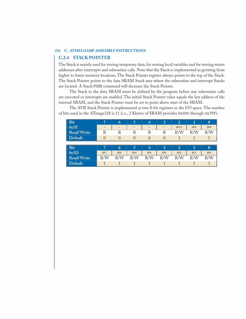
234 C. ATMEGA328P ASSEMBLY INSTRUCTIONS
C.2.4 STACK POINTERThe Stack is mainly used for storing temporary data, for storing local variables and for storing returnaddresses after interrupts and subroutine calls. Note that the Stack is implemented as growing fromhigher to lower memory locations. The Stack Pointer register always points to the top of the Stack.The Stack Pointer points to the data SRAM Stack area where the subroutine and interrupt Stacksare located. A Stack PUSH command will decrease the Stack Pointer.
The Stack in the data SRAM must be defined by the program before any subroutine callsare executed or interrupts are enabled. The initial Stack Pointer value equals the last address of theinternal SRAM, and the Stack Pointer must be set to point above start of the SRAM.
The AVR Stack Pointer is implemented as two 8-bit registers in the I/O space. The numberof bits used in the ATmega328 is 11 (i.e., 2 Kbytes of SRAM provides 0x000 through 0x7FF).
Bit 7 6 5 4 3 2 1 00x5E - - - - - SP10 SP9 SP8
Read/Write R R R R R R/W R/W R/WDefault 0 0 0 0 0 1 1 1
Bit 7 6 5 4 3 2 1 00x5D SP7 SP6 SP5 SP4 SP3 SP2 SP1 SP0
Read/Write R/W R/W R/W R/W R/W R/W R/W R/WDefault 1 1 1 1 1 1 1 1

235
A P P E N D I X D
Example C/C++ SoftwareCoding Guidelines
D.1 INTRODUCTIONIt is well accepted in industry that creating high-quality software requires source code to be consistent,modular and self-documenting. Software is unique in that, often, large teams of engineers will workon the same project over a long period of time. For example, my first engineering job was withMotorola in which I joined a team of 30 software engineers that had been working on a projectfor over five years. Imagine a fresh-out engineer coming onto a project containing millions of lines-of-code. If it were not for strict coding guidelines, I would never have been able to overcome thelearning curve in a timely manner. Ever since, I have been an advocate of good software engineeringpractice.
Motorola recognized that the quality of software was directly related to the maintainabilityof the source code. In fact, engineers working on my project were not allowed to check in theirwork until it underwent a strict peer-review process. One of the corner-stones of the review involvedconsistency checks against a set of software coding rules for the group. One of the most importantaspects to developing high-quality software is consistency among source files on a large project.Consistent source-code listings allow a higher degree of maintainability, as engineers are able toanalyze software as a whole without the difficulty of switching from style to style. Unfortunately,the skill of writing consistent software is grossly neglected within most academic environments asmany don’t recognize its importance.
The remainder of this appendix contains an actual example C/C++ Software Coding Guide-lines document compiled by Jim Preston of RELM Wireless Corp. This document represents thevery minimum set of rules that many companies would use as a standard. Note that some rules havebeen removed, as they represent very specific features of the project.
D.1.1 PURPOSEThis document contains recommendations for the development of C/C++ software within (a com-pany). The purpose of these recommendations is to promote the readability and maintainability ofsource code among multiple developers. This is a living document and subject to revision.
The recommendations are based on established standards collected from a number of sources,including individual experience, local requirements, and suggestions from the sources cited at theend of this document.

236 D. EXAMPLE C/C++ SOFTWARE CODING GUIDELINES
D.1.2 PHILOSOPHYD.1.2.1 Code
• Code should be kept as simple and straightforward as possible.
• In the context of having proper architecture and design documentation, code should be writtenin a self-documenting manner.
• Optimization should only be done when proven to be necessary.
D.1.2.2 Comments• Comments are not meant to take the place of separate architecture and design documentation.
• Comments should be meaningful, and they should not repeat what is stated in the code itself.
• Anything that is not obvious should be commented.
• Comments should be updated as the code is updated.
D.1.2.3 EditorsWhile a specific editor can enhance the readability of code by color coding, automatic formatting,etc., the code should not rely on such features to be readable. Source code should be written in a waythat maximizes its readability independent of any editor.
D.1.3 FORMATD.1.3.1 Layout of the RecommendationsThe recommendations are grouped by topic, and each recommendation is numbered to make refer-ences easier during reviews.
Recommendations have the following format:
n. Recommendation short description.Example (if applicable)Motivation, background and additional information.
D.1.3.2 Recommendation ImportanceThe terms must, should and can have special meaning. A must requirement must be followed, shouldis a strong recommendation, and can is a general guideline.
D.2. GENERAL RECOMMENDATIONS 237
D.2 GENERAL RECOMMENDATIONS
1. Any violation to the guide is allowed if it enhances readability.
It is impossible to cover all the specific cases in a general guide and the developer shouldbe flexible.
2. The rules can be violated if there are strong personal objections against them.
The attempt is to make a guideline,not to force a particular coding style onto individuals.
D.3 NAMING CONVENTIONS
3. Names representing types should be in mixed case starting with upper case.Line , SavingsAccount
Common practice in the C++ development community.
5. Variable names should be in mixed case starting with lower case.line , savingsAccount
Common practice in the C++ development community. Makes it easy to distinguishvariables from types, and effectively resolves potential naming collisions as in the fol-lowing declaration:
Line line;
6. C++ function names should be in mixed case starting with upper case.SetName (), CurrentIndex ()
Common practice in the C++ development community.
7. For C function names, underscores should be used to separate module abbrevia-tions from the rest of the name. The use of two consecutive underscores should beavoided.MM_Initialize ()
Helps to locate function definitions within files.
8. Underscores must not be used at the beginning or end of an identifier._TaskCounter // NOmessageIndex_ // NO
This convention is often reserved for system purposes.

238 D. EXAMPLE C/C++ SOFTWARE CODING GUIDELINES
9. Global variables must be prefixed with g_.g_globalCounter
Distinguishes global variables from other variables. In general, the use of global variablesshould be avoided.
10. Private class variables must be prefixed with m_.classclassclass CSomeClass{
privateprivateprivate:intintint m_length;
}
Indicating class scope by using an “m_” prefix makes it easy to distinguish class variablesfrom local variables.
11. Named constants (including enumeration values) must be all uppercase usingunderscore to separate words.MAX_ITERATIONS , COLOR_RED , PI
This is common practice in the C++ development community.
12. Enumeration constants can be prefixed by a common type name.enumenumenum Color{
COLOR_RED ,COLOR_GREEN ,COLOR_BLUE
};
This gives additional information of where the declaration can be found,which constantsbelong together, and what concept the constants represent.An alternative approach is to always refer to the constants through their common type:Color::RED, Airline::SOUTHWEST, etc.
D.4 LAYOUT
13. Basic indentation should be 4 spaces.forforfor (i = 0; i < numElements; i++){
m_elements[i] = 0;}
This is a common indentation amount. Editors should be set to use spaces in place oftabs.

D.4. LAYOUT 239
14. Block layout should be as illustrated in example 1 below, and it must not be asshown in examples 3 or 4.// Example 1whilewhilewhile (!done){
DoSomething ();done = MoreToDo ();
}
// Example 2whilewhilewhile (!done) {
DoSomething ();done = MoreToDo ();
}
// Example 3whilewhilewhile (!done)
{DoSomething ();done = MoreToDo ();}
// Example 4whilewhilewhile (!done)
{DoSomething ();done = MoreToDo ();
}
The styles in examples 3 and 4 don’t emphasize the logical structure of the code asclearly as examples 1 and 2. Example 4 introduces an extra indentation level.The choice between examples 1 and 2 is largely a matter of personal preference. How-ever, standardizing on a particular style enhances readability. One argument in favor ofexample 1 is that brackets are generally easier to find when they are put on their ownline.

240 D. EXAMPLE C/C++ SOFTWARE CODING GUIDELINES
15. Class declarations should have the following form:classclassclass CSomeClass : publicpublicpublic CBaseClass{
publicpublicpublic:...
protectedprotectedprotected:...
privateprivateprivate:...
}
This partially follows from the general block rule above. The ordering is “most publicfirst,” so people who only wish to use the class can stop reading when they reach theprotected/private sections. Sections that are not applicable should be left out.
16. A switchswitchswitch statement should have the following form:switchswitchswitch (condition){
casecasecase ABC:statements;breakbreakbreak;
casecasecase DEF:casecasecase XYZ:
statements;breakbreakbreak;
defaultdefaultdefault:statements;breakbreakbreak;
}
Individual casecasecase blocks should be separated by a blank line after the breakbreakbreak statement.switchswitchswitch statements should always include a defaultdefaultdefault case to catch errors.
D.4. LAYOUT 241
17. Single-statement ififif-elseelseelse,forforfor and whilewhilewhile statements should have brackets.ififif (condition){
statement;}
// NOTififif (condition)
statement;
The primary motivation for this recommendation is so that single-statement and multi-statement forms of these constructs have a consistent layout. This enhances readability.
18. Whitespace:
• Conventional operators should be surrounded by a space.
• C++ reserved words should be followed by a space.
• Commas should be followed by a space.
• Semicolons in forforfor statements should be followed by a space.a = (b + c) * d; // NOT: a=(b+c)*d
whilewhilewhile (truetruetrue) // NOT: while(true){
...}
DoSomething(a, b, c, d); // NOT: DoSomething(a,b,c,d);
forforfor (i = 0; i < 10; i++) // NOT: for(i=0;i<10;i++){
...}
returnreturnreturn value;
Makes the individual components of the statements stand out. Enhances readability.
19. Expressions should be fully parenthesized.total = CURRENCY * (dollars + change);
Enhances readability and prevents some calculation mistakes.
242 D. EXAMPLE C/C++ SOFTWARE CODING GUIDELINES
20. For a function with a large number of arguments, the function should be declaredwith one variable per line.voidvoidvoid GetTotal (constconstconst voidvoidvoid* itemOne ,
constconstconst voidvoidvoid* itemTwo ,constconstconst voidvoidvoid* itemThree ,constconstconst voidvoidvoid* itemFour ,constconstconst voidvoidvoid* itemFive ,constconstconst voidvoidvoid* itemSix);
Enhances readability. Also allows commenting each of the parameters individually ifnecessary.
D.5 STATEMENTS
D.5.1 TYPES
21. Types that are local to one file only can be declared inside that file.
Enforces information hiding.
D.5.2 VARIABLES
22. Variables should be declared one per line.
Enhances readability for both variable declaration and initialization.
23. Variables must not have dual meaning.
Enhances readability. Reduces chance of error by variable side effects.
24. Variables should be declared in the smallest scope possible.
Keeping the operations on a variable within a small scope, makes it is easier to controlthe effects and side effects of the variable.
D.5. STATEMENTS 243
25. Class variables should not be declared public.
The concept of C++ information hiding and encapsulation is violated by public variables.Use private variables and access functions instead.One exception to this rule is when the class is essentially a data structure, with nobehavior (equivalent to a C structstructstruct). In this case, it is appropriate to make the class’instance variables public.
26. C++ pointers and references should have their reference symbol next to the typerather than next to the name.floatfloatfloat* x; // NOT: float *x;intintint& y; // NOT: int &y;
The “pointer-ness” or “reference-ness” of a variable is a property of the type rather thanthe name.
D.5.3 LOOPS
27. Only loop control statements should be included in forforfor() constructs.sum = 0; // NOT:forforfor (i = 0; i < 100; i++) // for (i = 0, sum = 0; i < 100; i++){ // {
sum += value[i]; // sum += value[i];} // }
This increases readability and maintainability. It makes a clear distinction between loopcontrols and loop content.
28. The use of breakbreakbreak and continuecontinuecontinue should be avoided, except for the standard use ofbreakbreakbreak in switchswitchswitch statements.
These statements should only be used if they produce higher readability than theirstructured counterparts.
244 D. EXAMPLE C/C++ SOFTWARE CODING GUIDELINES
D.5.4 CONDITIONALS
29. Executable statements in conditionals should be avoided.File* fileHandle = open(fileName , "w");ififif (! fileHandle){
...}
// NOT:ififif (!( fileHandle = open(fileName , "w"))){
...}
Conditionals with executable statements are difficult to read.
D.5.5 FUNCTIONS
30. Function arguments that are not altered within the function, and are passed byreference, should be passed with the constconstconst type qualifier.voidvoidvoid* GetTotal(constconstconst voidvoidvoid* itemOne , constconstconst voidvoidvoid* itemTwo){
...}
This protects the variables from alteration and indicates that intent to the reader.
D.5. STATEMENTS 245
D.5.6 MISCELLANEOUS
31. Split lines must be made obvious.totalSum = a + b + c +
d + e;
ififif (conditionOne &&conditionTwo)
someSetting = (settings & SOME_MASK) >>SOME_SHIFT;
It is difficult to give rigid rules for how lines should be split, but in general:
• Break after a comma.
• Break after an operator.
• Align the new line with the beginning of the expression on the previous line.
32. If a complex expression is split over several lines, the logic of the expressionshould be made clear through the placement of the line breaks.ififif (( conditionOne && conditionTwo) ||
(conditionThree && conditionFour))
// NOTififif (( conditionOne && conditionTwo) || (conditionThree &&
conditionFour))
Enhances readability.
33. The use of hard-coded magic numbers should be avoided. Numbers other than0 and 1 should be declared as named constants instead.
If the number does not have an obvious meaning by itself, readability is enhanced byintroducing a named constant instead.
34. If a named constant definition includes logic or arithmetic operations, the entiredefinition should be surrounded with parentheses.###definedefinedefine PI 3.141590210###definedefinedefine FOUR_PI (4 * PI)
Named constants are replaced by their defined value wherever they appear in code.Without parentheses, this can introduce problems with the order of operations.

246 D. EXAMPLE C/C++ SOFTWARE CODING GUIDELINES
35.gotogotogoto should not be used.
gotogotogoto statements violate the idea of structured code. Only in a few cases (for instance,breaking out of deeply nested structures) should gotogotogoto be considered, and only if thealternative structured counterpart is less readable.
36. The use of macros should be kept to a minimum.
While they are useful, macros make debugging more difficult. Code within a macroshould be simple and well understood, and should be kept to a few lines.
37. In general, there should be only one exit point from a method.
Multiple exit points (i.e., returnreturnreturn statements in the middle of a method) should not beused unless they improve readability.
D.6 COMMENTS
39.###endifendifendif preprocessor statements should always be followed by a comment.###ifdefifdefifdef USE_BLOCK
. . .
###endifendifendif // USE_BLOCK
The reader will either be able to see the beginning statement on the screen or a comment.The comment can be either an explanation or simply a copy of the code that began theblock.
40. Comments should in general be above the statements being commented, not tothe side.// Some commentstatement
//NOTstatement // Some comment
It may be more readable, in some cases, to put the comments for variable declarationsand parameter lists to the right of the statement.

D.7. FILES 247
D.7 FILES
41. Classes and modules should be declared in a header file and defined in a sourcefile where the names of the files match the name of the class/module.MyClass.h, MyClass.cpp
This makes it easy to find the associated files of a given class.
42. File content should be kept within 110 columns.
Excessively long lines hinder readability.
43. Header files must contain an include guard.###ifndefifndefifndef _FILENAME_H_###definedefinedefine _FILENAME_H_:[header file body].
:###endifendifendif // _FILENAME_H_
Include guards protect against multiple inclusions.
44. Include statements should be sorted and grouped. They should be sorted bytheir hierarchical position in the system with low level files included first.###includeincludeinclude <fstream >###includeincludeinclude <iomanip >###includeincludeinclude "PropertiesDialog.h"###includeincludeinclude "MainWindow.h"
It gives an immediate clue about which modules are used.Include file paths must never be absolute. Compiler directives should be used insteadto indicate root directories for includes.


249
Bibliography
R. H. Katz, Contemporary Logic Design, second edition, Prentice Hall. 6
S. Brown and Z. Vranesic, Fundamentals of Digital Logic with VHDL Design, third edition, McGraw-Hill. 6
B. W. Kernighan and D. M. Ritchie, The C Programming Language, second edition, Prentice Hall.23
Arduino, 2010, http://www.arduino.cc/. 81
ATMEL, 8-bit AVR Microcontroller with 4/8/16/32K Bytes In-System Programmable Flash, Rev.8161D - 10/2009, Atmel Corporation. 85, 95, 96, 97, 100, 101, 103, 105, 107, 119, 140, 154,179, 212, 213, 214
ATMEL, 8-bit AVR Microcontrollers JTAGICE mkII Quick Start Guide, Rev. 2562C - 07/2006,Atmel Corporation. 89
ATMEL, AVR ONE! Quick-start Guide, Rev. 32104B - 02/2010, Atmel Corporation. 89


251
Author’s Biography
DAVID J. RUSSELLDavid J. Russell received the B.S. degree in computer engineering andthe M.S. degree in electrical engineering from the University of Ne-braska, Lincoln, Nebraska, in 1996 and 2001, respectively. Currently,he is a Ph.D. candidate in the Department of Electrical Engineering ofthe University of Nebraska-Lincoln. His research interests include dig-ital signal processing,wireless communications, and biological sequenceanalysis. From 1996 to 1997, he was with Motorola Space and SystemsTechnology Group, Scottsdale, Arizona, where he was a software engi-neer. From 1997 to 2004, he was with EFJohnson, Lincoln, Nebraska,where he was a principal development engineer. Since 2004, he has beenwith the University of Nebraska, Lincoln, where he currently serves asLecturer. Additionally, he has worked as a contract engineer for Telex,a part of Bosch Security Systems. Most recently, he helped create andpresently works for the contract engineering company Red-Cocoa.


253
Index
ADC, 135ALU, 5ANSI C, 23architecture, 95Arduino, 79arguments, 25arrays, 58ASCII, 17assembly language, 24assignment statements, 32
BCD, 16big-endian, 9binary, 6bits, 6block, 25boot loader, 79bug, 87byte, 7
clock, 4comments, 30compile-time errors, 87context, 148CPU, 5
DAC, 136debounce, 111debugging, 87decimal, 7declaration, 31dereferencing operator, 57
digital, 5
EEPROM, 80, 211embedded system, 1extern keyword, 52
floating, 104fprintf(), 26full duplex, 170function, 25, 51function pointer, 67function prototypes, 52
GPIO, 99
H Bridge, 111half duplex, 170hardware, 4Harvard architecture, 96hex, 7hexadecimal, 7
I2C, 169IDE, 79IIC, 169inline comments, 30ISR, 148
library function, 25little-endian, 9LSB, 9
machine instructions, 24

254 INDEX
machine language, 5macro, 38members, 70memory leak, 63MSB, 9
nibble, 7noise margin, 5
Ones’ Complement, 10overflow, 13, 34
peripheral device, 2pin-muxing, 100pointer, 56polling, 106, 147printf(), 26program, 4protocol, 167PWM, 115
register keyword, 55registers, 5
ADCADCH, 143ADCL, 143ADCSRA, 142ADCSRB, 143ADMUX, 140DIDR0, 144
Analog ComparatorACSR, 144DIDR1, 145
EEPROMEEARH, 214EEARL, 214EECR, 215EEDR, 214
GPIODDRB, 108
DDRC, 108DDRD, 109PINB, 108PINC, 109PIND, 109PORTB, 108PORTC, 108PORTD, 109
InterruptsACSR, 163ADCSRA, 163EECR, 164EICRA, 154EIFR, 155EIMSK, 154PCICR, 155PCIFR, 155PCMSK0, 156PCMSK1, 156PCMSK2, 156SPCR, 160SPSR, 161TIFR0, 157TIFR1, 159TIFR2, 160TIMSK0, 157TIMSK1, 158TIMSK2, 159TWCR, 162UCSR0A, 161UCSR0B, 162
SPISPCR, 182SPDR, 183SPSR, 183
Timer0OCR0A, 123OCR0B, 123TCCR0A, 120

INDEX 255
TCCR0B, 122TCNT0, 123
Timer1ICR1H, 128ICR1L, 128OCR1AH, 127OCR1AL, 127OCR1BH, 128OCR1BL, 128TCCR1A, 123TCCR1B, 125TCCR1C, 126TCNT1H, 127TCNT1L, 127
Timer2OCR2A, 132OCR2B, 132TCCR2A, 128TCCR2B, 130TCNT2, 131
TimersASSR, 132GTCCR, 133
TWITWAMR, 182TWAR, 181TWBR, 179TWCR, 179TWDR, 180TWSR, 180
USART0UBRR0H, 187UBRR0L, 187UCSR0A, 184
UCSR0B, 185UCSR0C, 186UDR0, 184
RISC, 95RS-232, 171RS-485, 171run-time errors, 87
scope, 52self-documenting code, 33Sign and Magnitude, 10sign bit, 10sign-extension, 33sketch, 79snprintf(), 26software, 4SPI, 170sprintf(), 26statement, 25static keyword, 54structure, 69
TWI, 170Two’s complement, 11type, 31type cast, 36
UART, 171union, 74USART, 171
variable, 25volatile keyword, 56von Neumann architecture, 96
Wiring, 79


