Fabien De Groote,Jean-Pierre Teyssier, Tony Gasseling,Olivier Jardel, and Jan Verspecht
In this article, we will introduce you to measurements for powertransistor characterization: why they matter, why they are such acomplicated, highly specialized field, and where we think the tech-nology of power transistor characterization is headed. To accom-plish this goal, we will use simple examples and explanations, at
the risk of oversimplifying the matter. For those individuals who want todive deeper into the subject, we provide plenty of references. Note thatthe list of references is far from complete, but we are convinced that it isa good starting point. If you are already an expert in the field, there maybe little chance that you will learn new things; nevertheless, we hope thatyou can still enjoy the reading. Please note that we restrict ourselves asmuch as possible to the characterization aspects, and only refer to model-ing aspects if they are useful in the context of transistor characterization.
Why Power Transistor Characterization Matters The microwave power amplifier is the workhorse of the wireless com-munications industry. It converts simple dc power into complex radio
Fabien De Groote is with Verspecht-Teyssier-DeGroote, Brive-la-Gaillarde, France. Jean-Pierre Teyssier and Olivier Jardel are with
XLIM, Limoges, France. Tony Gasseling is with AMCAD Engineering, Limoges, France. Jan Verspecht is with Jan Verspecht b.v.b.a., Opwijk, Belgium.
June 2008 71
waves that travel through space to enable wireless com-munication. Designing power amplifiers is a dauntingtask [1]. One reason is that many strict regulationsapply—for example, limitations on the creation ofundesired spectral components [often quantified byadjacent-channel power ratio (ACPR)] and limitationson the maximum allowable distortion of the informa-tion carried by the radio waves [often quantified byerror vector magnitude (EVM)]. These regulationsmake a lot of sense since the spectrum gets increasing-ly crowded and there is a need to prevent interferencecaused by undesired spectral components generated byyour neighbor’s power amplifier, while at the sametime making sure that the information that you getwhile talking to your partner is undistorted. As it turnsout, you don’t need a lot of distortion to turn “I do” into“I don’t,” with potentially disastrous consequences. Butthere is another reason why the design of power ampli-fiers is daunting. Whereas the power amplifier is theworkhorse of the wireless communications industry,the power transistor inside the power amplifier is itsproblem child. In other words, power transistors oftendon’t behave the way the designer expects. It is theresponsibility of the power amplifier designer to makesure that he or she can integrate the problem child tran-sistor into a well-behaved power amplifier that obeysstrict regulations. If you are a parent (or a problemchild) yourself, you will certainly understand the issue.
Fortunately, the designer is not alone since he or shecan get help from the transistor modeler. A transistormodeler is someone who interacts with the transistorthrough a multitude of experiments and who extracts amathematical model from the measured data. Thismodel describes how the transistor behaves under awide range of excitation signals and operating condi-tions. This mathematical model is nothing more than adescription of the relationship between the voltagewaveforms and the current waveforms as they appearat the transistor terminals. The transistor model is thenused by the designer in a simulator to predict the per-formance of any amplifier circuit containing the mod-eled transistor, even before the amplifier is actuallybuilt. The designer can quickly optimize the parametersof his or her design in the simulator to make sure thatthe design will meet the desired specifications. Onlythen will a prototype of the amplifier be built and test-ed. If the model is a good one, the prototype amplifierwill meet the specs and the designer can proudlyinform his or her manager that the design project iscompleted! If the designer is lucky, he or she may evenget a raise. If the model is not a good one, however, theprototype amplifier will not meet the specs. But that isnot all. If the model is bad, the designer may have noclue at all about what to do to improve the design andthe only alternative is often an inefficient trial-and-errordesign approach. Needless to say, under these circum-stances, the designer needs to be really, really lucky to
get a raise. The above clearly illustrates the value of agood transistor model as it greatly influences the timeto market of any power amplifier design.
So what does it take to get a good model? The tran-sistor modeler starts by gathering knowledge about thephysical parameters of the transistor: doping profiles,physical dimensions, number of fingers, etc. This infor-mation is sufficient to get a rough idea about the oper-ating region of the transistor—for example, maximumvoltage or current, maximum power dissipation, orbreakdown voltage. The physical information is alsosufficient to get an idea of the mathematical structure ofthe relationship between the voltage and current wave-forms. For example, knowing that the transistor is afield-effect transistor (FET) is sufficient information toknow that the drain current is mainly a function of thegate voltage, whereas knowing that the transistor is abipolar junction transistor (BJT) is sufficient informa-tion to know that that the collector current is mainly afunction of the base current.
Next, the transistor modeler applies a variety of sig-nals to the transistor terminals and measures quantitiesthat are related to the voltage and current waveforms.The quantities that are measured can be the instanta-neous values of the voltages and currents themselves,but can also be other derived quantities like S-parame-ters, or the time averaged values of the voltages and cur-rents. The trick is to apply a minimum number of excita-tion signals that allows the modeler to determine allunknown parameters of the model. This is called theproblem of experiment design. Once the modeler hasdetermined all the parameters of the model, he or shewill try to find a mathematical relationship between thevoltage waveforms and current waveforms that is consis-tent with the measured quantities. If the assumed mathe-matical structure of the model is complete, the model willbe capable of predicting the relationship between the volt-age waveforms and current waveforms under a range ofexcitation signals that is much wider than the range ofexcitation signals used during the model extraction.
If in doubt, the modeler will verify assumptions onthe mathematical structure of the model by performingmodel validation experiments. The idea of model valida-tion is to provide excitation signals that are as close aspossible to the signals that will be seen by the transistorin a final application, and to verify whether the modelcan predict the measured results. If the model succeedsin the validation test, the modeler is ready to transfer themodel to the designer. Note that the signals that are usedfor model extraction are usually much different from thesignals that the transistor will see in a final application.
The process of designing the experiments and per-forming the transistor measurements, for the purposeof model extraction as well as model validation, iswhat we call “transistor characterization.” It is clearfrom the above discussion that good power transistorcharacterization is an indispensable tool for building
72 June 2008
good transistor models. To summarize, power transis-tor characterization matters because it is vital for build-ing good transistor models, which are necessary fordesigning good amplifiers capable of ensuring clearconversations with our partners on our mobile phones.
Why Microwave Power TransistorCharacterization People Arrive Late at PartiesOne may wonder why microwave power transistorcharacterization is so difficult. Many engineers proba-bly remember characterizing simple BJTs in the studentlab. It is really easy. One injects a current IB into thebase of the junction transistor, applies a voltage VCE
across the collector and emitter, and simply measuresthe corresponding collector current IC and the corre-sponding base-emitter voltage VBE. This measurementis then repeated for a whole range of base currents andcollector voltages. If performed with enough resolu-tion, this process results in two measured, two-dimen-sional (2-D) functions FBE(., .) and FC(., .) that describeVBE and IC as a function of VCE and IB
VBE = FBE(VCE, IB) (1)
IC = FC(VCE, IB) . (2)
If we are dealing with an FET, we do a similar set ofmeasurements whereby we apply gate voltages (VG) anddrain voltages (VD), and we measure the correspondinggate current (IG) and drain current (ID). This results intwo measured, 2-D functions FG(., .) and FD(., .) thatdescribe IG and ID as a function of VG and VD
IG = FG(VG,VD) (3)
ID = FD(VG,VD) . (4)
And we are done—the transistor is characterized andwe can go party. We only need to send the measured datato the transistor modeler, who constructs an equivalentelectrical network that behaves according to (1) and (2).This equivalent electrical network is the actual transistormodel. It runs in the simulator and can be used by thedesigner to optimize his design. Note that, since this arti-cle is about transistor characterization, we will not fur-ther elaborate on the modeling process itself.
So, why wouldn’t that kind of data be sufficient tomodel a microwave power transistor? In other words,why is it that people who characterize microwavepower transistors are often still measuring at a timewhen many others are partying? The answer is actuallypretty simple: this is first of all because of the“microwave,” and secondly because of the “power.”
The Microwave AspectWe will first elaborate on the “microwave” aspect. If wewere to explain to a layperson what microwave signalsare [2], we could probably get away with saying thatthese are electrical signals that vary incredibly fast. In
fact, light travels less than a foot during the time it takesfor these signals to go up and down once. So, how isthis related to the fact that the microwave transistormodeler is not satisfied if we provide him/her with thesame measurements as before? Why can’t he or she justtell the designer to use the simulator to apply suchrapidly varying electrical voltage signals VG(t) andVD(t) to the simple extracted FET model of (3) and (4)to predict the corresponding currents ID(t) and IG(t)?
IG(t) = FG(VG(t),VD(t)) ? (5)
ID(t) = FD(VG(t),VD(t)) ? (6)
The answer is that the microwave voltage signalvaries so fast that even a relatively small capacitor,inevitably present in any FET device, will start drawinga significant capacitive current that will partly show upat the terminals. In a similar manner, any relativelysmall inductance, inevitably present in any transistorlayout, will start generating a significant inductive volt-age that will partly show up at the transistor terminals.This implies that any model, in order to accurately pre-dict the terminal currents, will need to contain capaci-tive as well as inductive elements. Assume for amoment that our modeler adds capacitive currents tothe model as illustrated by (3) and (4). The result, whichis actually the fundamental idea of the well-knownRoot modeling approach [3], is
IG(t) = FG(VG(t),VD(t)) + dQG(VG(t),VD(t))dt
, (7)
ID(t) = FD(VG(t),VD(t)) + dQD(VG(t),VD(t))dt
. (8)
Note that this is certainly not the only way that amodeler would add capacitive currents, but we restrictourselves to this case because it is great for educationalpurposes while at the same time actually being regular-ly used in industry. The functions QG(.) and QD(.) rep-resent the charge storage that occurs in parallel with theFET transistor terminals. Note that the actual Rootmodel is somewhat more sophisticated, and that we areusing a simplified version for the sake of illustrating thetransistor characterization issues rather than divinginto modeling issues.
The modeler will now tell you that the dc data thatyou provided is sufficient to model the FG(.) and FD(.)
parts, but contains no information at all on the chargestorage functions QG(.) and QD(.), since we have onlymeasured at constant VG and VD. In other words, dur-ing our measurements, the capacitive current is alwaysequal to zero. Note that a similar conclusion not onlyapplies to the Root model, but in general to all modelscontaining capacitive and inductive elements: one cansimply not extract any information on inductors andcapacitors from dc measurements. The question thenbecomes the following: What kind of characterization
June 2008 73
measurements can be performed to enable the modelerto characterize these capacitors and the inductors in themodel? It is clear that to extract that information weactually need to apply microwave signals to the tran-sistor terminals and measure the relationship betweenthe voltage and current waveforms.
If we operate in the microwave domain, S-parametermeasurements are obviously the measurement tech-nique of choice. The idea is then to apply a dc gate volt-age VG0 and a dc drain voltage VD0 and to measure thecorresponding gate current IG0, drain current ID0, andthe corresponding S-parameters. This is then repeatedacross the entire (VG,VD) operating range of the tran-sistor. Needless to say that this process results in a lot ofdata: two 2-D functions FG(., .) and FD(., .) and fourbias-dependent S-parameter functions S11(., .), S12(., .),S22(., .) and S21(., .). It is then the task of the modeler toidentify all of the inductors and capacitors in the modelby analyzing the additional S-parameter data. The factthat the S-parameter measurements contain sufficientdata to extract the inductive and capacitive elements ofthe model can be demonstrated by looking at the sim-plified Root model as described by (7) and (8). Considerthat one applies a gate voltage of VG0 and a drain volt-age of VDO to the FET. During the S-parameter mea-surement, a small microwave signal will excite thedevice, resulting in fast voltage and current variations.Let us denote these variations by vg(t) for the gate volt-age variation, vd(t) for the drain voltage variation, ig(t)for the gate current variation, and id(t) for the drainvoltage variation. We can then write
IG0 + ig(t) = FG(VG0 + vg(t),VD0 + vd(t))
+ dQG(VG0 + vg(t),VD0 + vd(t))dt
,
(9)
ID0 + id(t) = FD(VG0 + vg(t),VD0 + vd(t))
+ dQD(VG0 + vg(t),VD0 + vd(t))dt
.
(10)
Since the time-varying deviations are small, theabove equations reduce to
ig(t) = ∂FG
∂Vgvg(t) + ∂FG
∂Vdvd(t) + ∂QG
∂Vg
dvg(t)dt
+ ∂QG
∂Vd
dvd(t)dt
. (11)
id(t) = ∂FD
∂Vgvg(t) + ∂FD
∂Vdvd(t) + ∂QD
∂Vg
dvg(t)dt
+ ∂QD
∂Vd
dvd(t)dt
. (12)
Note that each of the partial derivates in the aboveequation is constant during each S-parameter measure-ment and is evaluated in (VG0,VDO). Next one converts(11) and (12) to the frequency domain. The result is
Ig(ω) =(
∂FG
∂Vg+ ∂QG
∂Vgjω
)Vg(ω)
+(
∂FG
∂Vd+ ∂QG
∂Vdjω
)Vd(ω) , (13)
Id(ω) =(
∂FD
∂Vg+ ∂QD
∂Vgjω
)Vg(ω)
+(
∂FD
∂Vd+ ∂QD
∂Vdjω
)Vd(ω) . (14)
Equations (13) and (14) reveal that there is a simplerelationship between the partial derivatives of thecharge storage functions and the imaginary part ofthe Y-parameters. Assuming that port 1 is connectedto the gate of our transistor and port 2 is connected tothe drain, one finds that
ImY11(ω) = ∂QG
∂Vgω , (15)
ImY12(ω) = ∂QG
∂Vdω , (16)
ImY21(ω) = ∂QD
∂Vgω , (17)
ImY22(ω) = ∂QD
∂Vdω . (18)
The idea is then to measure bias-dependent S-para-meters and convert the S-parameters into Y-parame-ters. As shown by (15)–(18), the bias-dependent Y-parameters contain information on the partial deriva-tives of the charge storage functions. The modeler inte-grates the measured Y-parameters and can reconstructthe unknown charge storage functions. It is not hard toimagine that a similar approach will also give youinformation on the inductive effects, rather than thecapacitive effects. The essential conclusion is that bias-dependent S-parameters are necessary for determiningthe capacitive and inductive elements of the transistor.This principle does not only apply to the Root model,but in general applies to all modeling techniques.
The Power Aspect: ManyAmplifiers Are as Much ElectricalHeater as They Are Signal AmplifierSo we have performed a lot of measurements and wehave succeeded in gathering a lot of data: two 2-D func-tions FG(., .) and FD(., .) and four bias-dependent S-parameter functions S11(., .), S12(., .), S22(., .) andS21(., .). As stated before, this data should be sufficient
74 June 2008
to identify the static voltage and current parts of thetransistor model, as well as all of the inductive andcapacitive parts. In short, we can state that such a set ofmeasurements should be sufficient to characterize all ofthe pure electronic effects that are happening inside thetransistor. So why isn’t the modeler happy with thisdata? The answer is that the power transistor behavioris not just described by pure electronics. As stated earli-er, the power transistor is the component that convertsa lot of dc power into a lot of microwave power.Unfortunately, the power transistor does not only con-vert dc power into microwave power, it inevitably alsoconverts a significant portion of the dc power into heat.In many practical applications, only about half of the dcpower is converted into microwave power; the otherhalf is converted into heat. In fact, one can state thatmany state-of-the-art microwave power amplifiers areas much signal amplifier as they are electric heater;some of them are actually even more electrical heaterthan signal amplifier! The consequence of this is thatthe transistor may see a wide range of temperaturesduring the characterization measurements as well asduring its operation.
As it happens, some of the electronic elements of thetransistor are very sensitive to temperature. To illus-trate what the consequences are on the transistor characterization process, let us revisit the simple BJTexample described by (1) and (2). We once again applya constant base current IB0 and a constant collector-emitter voltage VCE0 to a power transistor, and we takea look at the digital multimeters measuring the corre-sponding base-emitter voltage VBE and the correspond-ing collector current IC. If the transistor is biased in itsactive region, we will note that IC slowly changes overtime, to finally settle to a steady-state value. Note thatsuch an effect, because of the time scale involved, can-not be explained by tiny inductors and capacitors sincewe are not applying any microwave frequency signal.The modeler may describe such a phenomenon byintroducing the temperature (T) as an explicit parame-ter in the model equations (or in the equivalent circuit,which we consider as just another way to represent themodel equations). The fact that the values of VBE and ICchange versus time can then easily be explained by thefact that the temperature of the transistor starts chang-ing due to self-heating as soon as we start our experi-ment. This can be expressed as
VBE(t) = FBE(VCE, IB, T(t)) , (19)
IC(t) = FC(VCE, IB, T(t)) . (20)
It is clear that a model can only be useful if it canaccurately describe the effect of the time-varying tem-perature. To do so, the modeler needs to introduce con-cepts from thermodynamics, like thermal conductance(Gth) and heat capacity (C th). To illustrate this fact, letus perform an approximate calculation of T(t).
At the beginning of our experiment, the transistortemperature will be equal to the room temperature T0.It will then start to rise because of the power dissipatedin the transistor. In order to model the time-varyingtemperature, we need to write down the thermody-namic equations of our system. We further assume thatour system can be represented by a heat capacity C th
and a thermal conductance Gth. The thermodynamicequation of our system becomes
d(CthT(t))dt
= P(t) − Gth(T(t) − T0) . (21)
This classic equation simply expresses that, at anymoment, the power dissipated in the transistor (P)
minus the power that is conducted out of the transis-tor by the conduction of heat (proportional to the tem-perature difference with the environment T − T0 andproportional to the thermal conductance Gth) is equalto the rate of change of the total heat stored in the tran-sistor (CthT). The introduction of the thermodynamicequations has direct consequences for the power tran-sistor characterization. Let us solve the combined setof (20) and (21) to calculate IC(t). For the sake of sim-plicity, we will start by linearizing (20). We alsoapproximate the dissipated power P by the product ofVCE and IC
P(t) =VCEIC(t) . (22)
The set of equations then becomes the following:
IC(t) = FC(VCE, IB, T0) + ∂FC
∂T(T(t) − T0) ,
(23)d(CthT(t))
dt=VCEIC(t) − Gth(T(t) − T0) . (24)
The above “textbook” set of two coupled linear dif-ferential equations can easily be solved with as initialcondition T(0) = T0. The solution for the temperatureT(t) is given by a simple first-order relaxation, asshown below:
T(t) = T0 + �T∞(1 − e−t/τ ) , (25)
where �T∞ is the steady-state temperature differencewith room temperature and τ is the relaxation time con-stant. The values of these parameters are given below:
�T∞ = VCEFC(VCE, IB, T0)
Gth −VCE∂FC∂T
(26)
and
τ = Cth
Gth −VCE∂FC∂T
. (27)
June 2008 75
The solution for the collector current is similar:
IC(t) = FC(VCE, IB, T0) + �I∞(1 − e−t/τ ) , (28)
with
�I∞ = ∂FC
∂T�T∞ . (29)
The above results reveal an interesting property ofthe coupled electrical and thermodynamic equations(the so-called electro-thermal equations). From (26) and(27), we can conclude that the transistor, from the ther-mal point of view, behaves as a system with a heatcapacity that is equal to Cth, but which has an apparentthermal conductance that is equal to the differencebetween the actual thermal conductance Gth and theproduct of VCE and the partial derivative of Fc(.) versustemperature T. We can conclude that if there is signifi-cant power dissipation in the transistor, we alwaysobserve a combination of thermal and electrical effects.
This can lead to interesting behavior. Suppose thatwe characterize a germanium bipolar transistor. Suchtransistors have a current gain that increases with tem-perature. The hotter the device, the more gain it has.This is mathematically expressed by
∂FC
∂T> 0 . (30)
Consider now the right-hand side of (27). For somebiasing conditions, especially at a high VCE, the denom-inator can become negative. This occurs when
VCE∂FC
∂T> Gth . (31)
Under those conditions, we see that the relaxationtime constant also becomes a negative number. Andthat means trouble! Putting the negative τ in (25) and(28), we come to the conclusion that the current as wellas the temperature will exponentially increase, neverto reach a steady-state value. This unstable positivefeedback phenomenon is called “thermal runaway.”The term is not only used in electronic engineering butalso in chemical engineering, where it is more com-monly known as a “big explosion.” Fortunately forelectronic engineers, the consequences of a thermalrunaway are less severe and usually only result in adamaged transistor (a little bit of smoke may still begenerated). Okay, so we have blown up one transistorand we go get another one. But how are we going tocharacterize the new device without also blowing itup? One way of breaking up the positive electro-thermal feedback cycle is to introduce a big enoughresistor in series with the VCE voltage source. The ideais that any increase in collector current will automati-cally decrease the collector voltage, decreasing the dis-sipated power, which then decreases the rate at whichthe temperature rises. This way we can characterize the
transistor across its entire operating span withoutblowing it up. From the above example, we can con-clude that it is hard to build one measurement setupthat allows you to characterize all possible transistortechnologies. One can imagine, for example, that anengineer is using the potentially unstable measure-ment setup during many years without blowing upany device due to thermal runaway simply because heis never measuring germanium transistors. One day,his manager gives him the task of characterizing a ger-manium transistor and, lo and behold, the “reliable”measurement system fails over and over again. Unlessthe engineer knows about thermal runaway, he willhave a hard time facing his manager.
Consider now a microwave power transistor. If weapply a particular bias, the temperature of the transis-tor will slowly change with a relaxation time constantthat can be anywhere from 200 ns to 1 ms, or evenlonger. At the same time, we can apply a microwavesignal. If we look at a particular performance parame-ter of the transistor, like S-parameters or power gain,we will see that these parameters will also slowly driftas the amplifier moves to a new equilibrium tempera-ture. Such an effect is called a “long-term memory”effect. In contrast, the dynamic effects caused by theinductors and capacitors described are sometimescalled “short-term memory” effects. The precise charac-terization and modeling of the long-term memoryeffects is actually one of the toughest challenges facedby today’s power transistor experts.
It is important at this point to state that long-termeffects are not exclusively caused by a time-varying tem-perature. Other physical effects inside the transistor,called trapping effects, can cause similar behavior. Thetrapping effect is a long-term memory effect related to thefact that the charge distribution in an FET is influenced bycharges that somehow get stuck in a trap and are onlyreleased after a relatively long time. These traps typicallyoccur on the surface of the transistor, although they cansometimes also be found in the bulk. The amount oftrapped charge is not a constant but depends on theregion where the transistor operates. Since the operatingregion may vary significantly during transistor operation,the trapping state will also vary, but only at a slow ratethat depends on how long it takes for the charge to bereleased by the trap after it has been captured.
Another important remark concerns the heat trans-fer (24). Equation (24) assumes that the thermal state ofthe transistor can be described by one temperature T(t).If we have a big power transistor, one can imagine thatthe temperature is not constant across the transistor, butis a function of the location. In other words, the tem-perature is described as a scalar field rather than oneparticular number. It is perfectly possible, for example,that there are significant temperature differencesbetween the fingers of the power transistor. In that case,the simple first-order model of (24) will not be sufficient
76 June 2008
to describe the thermal behavior of the transistor. Notethat it is not only the temperature that may vary insidethe transistor, but that the same holds for the dissipatedpower. From the modeling point of view, such a case isusually resolved by connecting a multitude of thermalnetworks.
Why Pulsed Measurements Provide AnswersSo how can we provide data to the modeler that allowshim or her to model the long-term memory effects? If weare dealing with thermal issues, the simplest way wouldbe to directly measure the temperature-dependentvoltage-current relationship, as illustrated below for abipolar transistor
VBE = FBE(VCE, IB, T) , (32)
IC = FC(VCE, IB, T) . (33)
This can only be done in practice if we apply a par-ticular couple of values {VCE, IB} for bipolar transistorsor {VGS,VDS} for FETs and a temperature T, and wemake sure that we measure {VBE, IC}—or respectively{IGS, IDS}—before the temperature has significantlychanged. Such a measurement is referred to as“isothermal.” From the hardware perspective, thisimplies that we need to have means to control the tem-perature of the transistor, like a thermal chuck, suchthat it has a temperature T when we start the experi-ment, and that we need to be able to apply {VCE, IB} or{VGS,VDS} and make a quick measurement of {VBE, IC}or {IGS, IDS} before there is any significant change ofthe device temperature. Since we want to do more thanone measurement, we switch {VCE, IB} or {VGS,VDS} off
as quickly as possible after the experiment. We thenwait until we are sure that the temperature hasreturned back to T before performing a subsequentmeasurement. If we can do all of this before there hasbeen a significant change in temperature, we are ableto directly measure the temperature-dependent{VBE, IC} or {IGS, IDS}. This process is called pulsed biasor pulsed IV (PIV) characterization.
Note that there are many ways to perform pulsedmeasurements. In general, a lot of insight into the trap-ping behavior as well as the thermal behavior can begained by not only changing the bias values during thepulse, but by also changing the initial bias values.
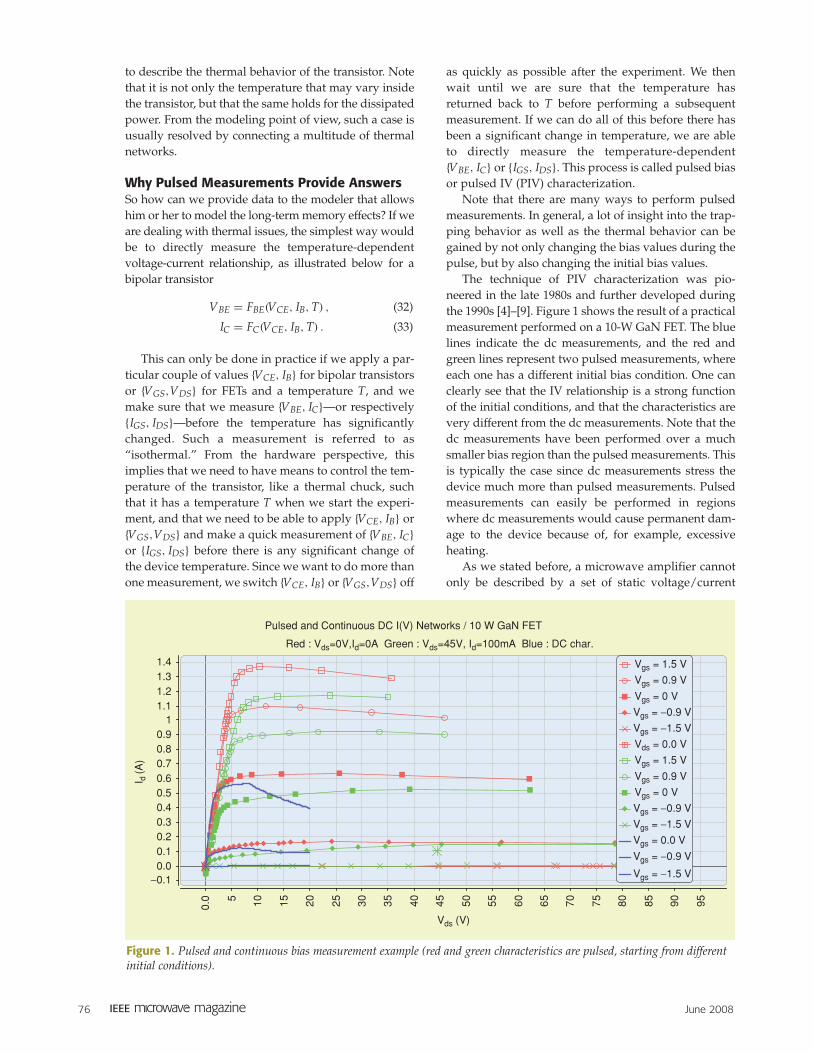
The technique of PIV characterization was pio-neered in the late 1980s and further developed duringthe 1990s [4]–[9]. Figure 1 shows the result of a practicalmeasurement performed on a 10-W GaN FET. The bluelines indicate the dc measurements, and the red andgreen lines represent two pulsed measurements, whereeach one has a different initial bias condition. One canclearly see that the IV relationship is a strong functionof the initial conditions, and that the characteristics arevery different from the dc measurements. Note that thedc measurements have been performed over a muchsmaller bias region than the pulsed measurements. Thisis typically the case since dc measurements stress thedevice much more than pulsed measurements. Pulsedmeasurements can easily be performed in regionswhere dc measurements would cause permanent dam-age to the device because of, for example, excessiveheating.
As we stated before, a microwave amplifier cannotonly be described by a set of static voltage/current
Figure 1. Pulsed and continuous bias measurement example (red and green characteristics are pulsed, starting from differentinitial conditions).
Pulsed and Continuous DC I(V) Networks / 10 W GaN FET
Red : Vds=0V,Id=0A Green : Vds=45V, Id=100mA Blue : DC char.
relationships. The model will also contain capacitiveand inductive effects that need to be characterized.And, unfortunately, these are also a function of tem-perature. The idea is then to also measure the bias-dependent S-parameters under well-controlled isother-mal conditions. Such measurements are called isother-mal pulsed-bias S-parameter measurements. AddingS-parameter capability to PIV measurements was pio-neered in the early 1990s [10], [11], and is still a hottopic today [12], [13]. A lot of excellent information onthe above topics can be found in [14]. A practical exam-
ple of pulsed-bias S-parameter measurements of a 20-W FET is shown in Figure 2.
Why Pulsed-Bias S-parameter Are Never EasyAlthough the basic principle of pulsed-bias S-parame-ter measurements is relatively simple, it is actually areal challenge to carry them out in practice. Consider,for example, a practical self-heating phenomenon with-in an FET as presented in Figure 3. The figure is derivedfrom a simulation and shows the temperature versus
Figure 3. Temperature increase of AlGaN/GaN HEMTs (SiC substrate), with a chuck temperature of 0◦C.
time when one applies an IV pulse to a transistor posedon a thermal chuck set at 0◦C. In this example, the tran-sistor gate measures 8 × 100 μm, and the pitch betweenthe different fingers is 35 μm (SiC substrate). For aninjected power of 5 W/mm, a thermal simulation usingAnsys software shows a temperature increase of 41.5◦Cduring the first 400 ns of the pulse. The temperature iscalculated for a finger located in the middle of the tran-sistor (the location of the temperature measurement isindicated by a point on the left). This simulation exam-ple shows that the transistor is not tested in isothermalconditions when applying IV pulse with a durationlonger than about 400 ns. This implies that, in order toprovide isothermal data to the modeler, we need to beable to measure the pulsed-bias S-parameters within atime span smaller than 400 ns. There are three mainchallenges to performing such a measurement, espe-cially for new technologies such as GaN transistors.
First of all there is the challenge of generating andmeasuring the fast bias excitation pulses, which needtransition times that are only a fraction of the pulsewidth, let’s say 30 ns. Using recent metal-oxide semicon-ductor field-effect transistor (MOSFET) technologies,existing pulsers can deliver pulses up to 240 V or 20 Awith an output resistance as low as 0.6 �. Figure 4 showsa typical voltage pulse shape obtained with a 200-MHzpulser delivering 100 V to a capacitance of 100 pF. These
new high-power MOSFET technologies, with shortswitching times, offer new and exciting measurementcapabilities for electro-thermal transistor modeling activ-ities. When performing such measurements, one has tobe very cautious about the presence of parasitic induc-tive and capacitive elements. Because of the steep slopesof the voltage and the current pulses, parasitic inductiveand capacitive elements can easily cause ringing effectsin the applied pulses as well as in the measured results.Parasitic small resistances can also distort the measure-ments. In fact, one needs a really careful design of thecabling between the pulses and the transistors. In gener-al, one always tries to minimize the cable lengths asmuch as possible and tries to place the pulsed-bias gen-erators as close as possible to the transistor terminals.Even then, it is a wise thing to characterize the parasiticbehavior of your cabling and to correct any errors causedby parasitics of the measurement setup.
Another issue is related to reliability. A completecharacterization of a transistor requires the applicationof extreme pulsed-bias conditions, for example near thetransistor breakdown area. Under such conditions, andwhen using a pulsed voltage generator, sudden break-down effects may generate a spectacularly big currentspike through the transistor. This current spike zaps thetransistor and can even reduce the transistor to nothingmore than a black spot on the wafer. To prevent thisfrom happening, one can introduce a serial resistancebetween the transistor and the pulser. The resistancewill then provide a robust and automated protection forbreakdown current spikes. Besides providing protec-tion, such resistive networks have other functionalities.A high input serial resistance associated with a pulsedvoltage generator behaves like a current source and canbe used to drive a bipolar transistor whereby one hasaccurate control of the pulsed input base current. Thisis especially interesting when the temperature of thetransistor changes and modifies the base-emitter diodecharacteristic. In addition, the resistive network canalso be adjusted to lower the risk of low-frequencyparametric oscillations. An example of a pulsed-bias
setup with a resistive net-work is shown in Figure 5.
All of the effects men-tioned above have to do withthe problem of performingpulsed-bias measurements.But the S-parameter mea-surements are also challeng-ing because they need to bemade under pulsed condi-tions. Between the early1990s and 2000s, the HP-8510 vector network analyz-er (VNA) was a popular toolfor making pulsed S-para-meter measurements. The
Figure 4. Example of 100-V pulse voltage measurementusing the latest pulser technology.
140
120
10080
60
4020
10 ns/div−20
0
Figure 5. Pulsed-bias measurement system with resistive network.
RS RSRS1 RS1RS2 RS2RL1 RL1RL2 OUT RL2
June 2008 79
instrument could make S-parameter measurements witha good dynamic range for all pulses having duration ofmore than 1 μs. Unfortunately, as explained previously,such a pulse width is too long for the isothermal charac-terization of certain modern power transistors. Using adifferent operating mode, called narrowband mode orasynchronous mode, VNAs could measure RF pulses asshort as 150 ns, but not without a severe desensitizationthat was proportional to the duty cycle. This could beresolved by averaging, but at the cost of significantlydecreasing the measurement speed. Today, improvedways of measuring pulsed scattering parameters havebecome readily available with the advent of a new gen-eration of VNAs. In addition to having better hardware,the dynamic range of pulsed measurements is furtherimproved by using techniques like hardware and soft-ware algorithms [12]. It is now possible to make pulsedS-parameter measurements in the X-band with adynamic range better than 50 dB using a pulse width of150 ns and a duty cycle of 0.001%.
Validating Models withLoad-Pull MeasurementsIsothermal pulsed-bias S-parameter measurementsallow the modeler to construct an equivalent electricalnetwork, called the transistor model. This model canrepresent the transistor in a simulator. If the modelerhas done a good job, the equivalent electrical networkthat he or she has built will behave in a way that isconsistent with the measured data. In other words, ifone were to simulate the isothermal pulsed-bias S-parameter measurements, the simulated response ofthe device would closely match the actual measureddata. At that point, the modeler can send the model tothe designer. One can then imagine the following con-versation taking place:
Designer: “How can you be so sure that yourmodel will correctly predict the transistor behav-ior for my amplifier design project?”
Modeler: “Well, if you would use that model tosimulate isothermal pulsed-bias S-parametermeasurements, the simulated data will preciselymatch the measured data.”
Designer: “I believe you. But I am not interestedin simulating isothermal pulsed-bias S-parametermeasurements. I need to simulate under realoperating conditions, with real signals. So I repeatmy question: How can you be so sure that yourmodel will correctly predict the transistor behav-ior for my amplifier design project?”
Modeler: “Well, I pretty much used the same kindof equivalent circuit that worked before. To makeit match the measured pulsed-bias S-parameter
data, I only had to add a tiny nonlinear capacitorto the circuit and I had to introduce one new para-meter to the mathematical function that describesthe nonlinear current source.”
Designer: “You actually had to add new things tothe existing model to match your data??? Now Iam really worried. I won’t start using your modelunless you show me that it also works under real-istic operating conditions!”
The idea is that a designer will simply not trust amodel derived from pulsed-bias S-parameter mea-surements unless the model has been experimentallycharacterized under realistic operating conditions.This leads us to a different branch of microwavepower transistor characterization where the goal is tovalidate a model and not to extract the parameters ofthe model. Model validation is done by stimulating atransistor with excitation signals that are very similarto the actual signals the device will experience in apower amplifier and by measuring certain characteris-tics that can be derived from the response signals,such as power gain and spectral regrowth. The design-er will start trusting a model only when it is capable ofaccurately predicting the derived quantities of interestto the designer, and over a range of excitation signalsthat matches the final application.
So what do validation systems look like? Refering tothe example conversation between the designer and themodeler, it is clear that the most significant differencewith the pulsed-bias S-parameter system will be thepower of the applied microwave signals. The validationsystem needs to apply microwave signals that, by them-selves, are able to sweep across the whole transistoroperating region, whereas a pulsed-bias S-parametersystem will only use relatively small microwave signalsand will cover the transistor operating region by meansof pulsing the bias. But power is not the only parameter;there are other, more subtle, differences. At microwavefrequencies, a pulsed-bias S-parameter system willalways terminate the transistor terminals into a 50-�load. In microwave power amplifiers, the transistor out-put is terminated in a wide range of impedances thatspans anywhere from about 1 � to about 200 �. Thisimplies that a validation system needs to provide threemain functions: exciting the transistor with sufficientmicrowave power, controlling the output impedance,and measuring the response signal of the transistor.Controlling the output impedance is often referred to as“load-pull,” which is why systems that have this capa-bility are called load-pull systems. In the following, wegive an overview of existing load-pull techniques. Notethat one sometimes also controls the output impedanceof the signal generator. This is called “source-pull.”
As described in [15], load-pull systems are typicallyclassified into two main categories: active and passive.
80 June 2008
In a passive load-pull system, the load impedance iscontrolled by passive tuners. The passive tuner is usu-ally mechanical in nature, whereby a metal part is mov-ing in a waveguide in order to create controllable reflec-tions. A good example is described in [16]. A small frac-tion of passive load-pull setups are actually electronicin nature and use diodes to generate a multitude ofreflection coefficients, as described in [17].
The major drawback of using a passive structure tocreate a controllable reflection is that one cannot com-pensate for any power that is dissipated between thedevice under test (DUT) and the passive structure thatgenerates the controllable reflection. This power dissipa-tion inevitably occurs in all components that are placedbetween the transistor terminal and the tuning elementssuch as probes, cables, couplers, diplexers, etc. As aresult, the maximum amplitude of the reflection coeffi-cient, as seen by the transistor, will always be smallerthan one. Depending on the amount of inevitable lossesin the measurement setup, the maximum amplitude ofthe reflection coefficient may become too small to be ofany use. This problem may be solved by using so-calledactive load-pull setups. These are setups in which oneintroduces one or more amplifiers to generate wave sig-nals that are sent towards the DUT output terminals. Theamplifier can potentially compensate for any losses andgenerate reflection coefficients with amplitudes equal toand even bigger than one.
A good example, illustrating the problems and benefits of active load-pull, is described in [18].Unfortunately, there are not only advantages to usingan active load-pull approach. The power handlingcapability of any active load-pull setup is limited by theamplifier that is used. This limits both the maximumpower handling capability as well as the frequencyrange over which one can synthesize impedances. Incontrast to the active load-pull setups, the maximumpower handling capability and frequency range of anypassive load-pull setup is only limited by passive struc-tures like cables, couplers, etc. Passive tuners typicallyoperate across multiple octaves and can handle powerlevels above 1 kW. Today, the vast majority of the load-pull setups use passive mechanical tuners. It is worth
noting that the typical mismatch of a GaN transistor isrelatively mild and within reach of most simplemechanical tuners, in contrast with silicon laterally dif-fused metal oxide semiconductor (LDMOS) transistorswhich have output impedances below 1 �.
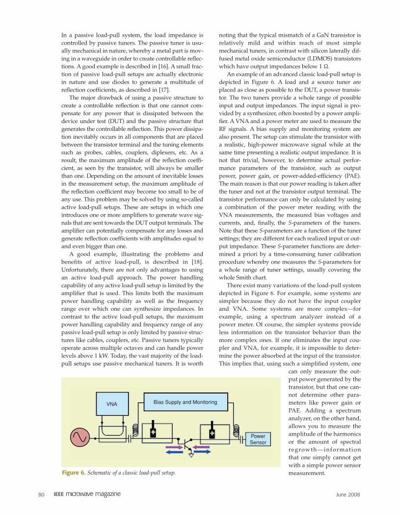
An example of an advanced classic load-pull setup isdepicted in Figure 6. A load and a source tuner areplaced as close as possible to the DUT, a power transis-tor. The two tuners provide a whole range of possibleinput and output impedances. The input signal is pro-vided by a synthesizer, often boosted by a power ampli-fier. A VNA and a power meter are used to measure theRF signals. A bias supply and monitoring system arealso present. The setup can stimulate the transistor witha realistic, high-power microwave signal while at thesame time presenting a realistic output impedance. It isnot that trivial, however, to determine actual perfor-mance parameters of the transistor, such as outputpower, power gain, or power-added-efficiency (PAE).The main reason is that our power reading is taken afterthe tuner and not at the transistor output terminal. Thetransistor performance can only be calculated by usinga combination of the power meter reading with theVNA measurements, the measured bias voltages andcurrents, and, finally, the S-parameters of the tuners.Note that these S-parameters are a function of the tunersettings; they are different for each realized input or out-put impedance. These S-parameter functions are deter-mined a priori by a time-consuming tuner calibrationprocedure whereby one measures the S-parameters fora whole range of tuner settings, usually covering thewhole Smith chart.
There exist many variations of the load-pull systemdepicted in Figure 6. For example, some systems aresimpler because they do not have the input couplerand VNA. Some systems are more complex—forexample, using a spectrum analyzer instead of apower meter. Of course, the simpler systems provideless information on the transistor behavior than themore complex ones. If one eliminates the input cou-pler and VNA, for example, it is impossible to deter-mine the power absorbed at the input of the transistor.This implies that, using such a simplified system, one
can only measure the out-put power generated by thetransistor, but that one can-not determine other para-meters like power gain orPAE. Adding a spectrumanalyzer, on the other hand,allows you to measure theamplitude of the harmonicsor the amount of spectralregrowth—informationthat one simply cannot getwith a simple power sensormeasurement.Figure 6. Schematic of a classic load-pull setup.
VNA
PowerSensor
Bias Supply and Monitoring
June 2008 81
Most load-pull systems control the load impedanceand perform power measurements only at the frequen-cy of the input signal, the so-called fundamental fre-quency. Any large-signal excitation of the power tran-sistor will not only generate output power at the fun-damental frequency, but also at multiples of the funda-mental frequency. These spectral components arecalled harmonics. As there is power in the harmonics,the overall behavior of the transistor will not onlydepend on the load impedance at the fundamental fre-quency but also on the load impedances at the har-monic frequencies. Some load-pull systems control theload impedance at the second and even the third har-monic frequency [16], [19], [20]. Such systems arecalled harmonic load-pull systems.
Load-Pull and Time DomainClassic load-pull systems allow one to verify whether amodel can accurately predict power levels under load-pull operating conditions. Unfortunately, power is notthe only parameter that is of interest. The modeler alsoneeds to validate the capability of his or her model todescribe other important aspects, such as breakdowneffects or forward gate conductance. A validation of themodel for such highly nonlinear effects can only beachieved by actually measuring the time-domain volt-age and current waveforms under realistic large-signaloperating conditions and comparing them with thetime-domain waveforms that result from a simulation.
Load-pull systems having the capability to providesuch time-domain voltage and current waveforms werefirst developed in the late 1990s [24], [25] by adding tun-ing technology to large-signal network analyzers [26].Large-signal network analyzer technology itself wasdeveloped during the late 1980s and the 1990s [21]–[23].Note that all of the power information that is measuredby a classical load-pull system can easily be derivedfrom the time-domain voltage and current waveforms.
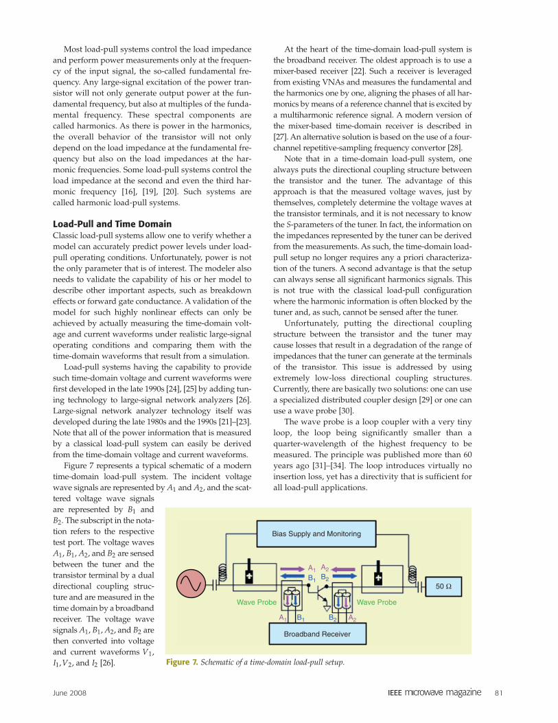
Figure 7 represents a typical schematic of a moderntime-domain load-pull system. The incident voltagewave signals are represented by A1 and A2, and the scat-tered voltage wave signalsare represented by B1 andB2. The subscript in the nota-tion refers to the respectivetest port. The voltage wavesA1, B1, A2, and B2 are sensedbetween the tuner and thetransistor terminal by a dualdirectional coupling struc-ture and are measured in thetime domain by a broadbandreceiver. The voltage wavesignals A1, B1, A2, and B2 arethen converted into voltageand current waveforms V1,I1, V2, and I2 [26].
At the heart of the time-domain load-pull system isthe broadband receiver. The oldest approach is to use amixer-based receiver [22]. Such a receiver is leveragedfrom existing VNAs and measures the fundamental andthe harmonics one by one, aligning the phases of all har-monics by means of a reference channel that is excited bya multiharmonic reference signal. A modern version ofthe mixer-based time-domain receiver is described in[27]. An alternative solution is based on the use of a four-channel repetitive-sampling frequency convertor [28].
Note that in a time-domain load-pull system, onealways puts the directional coupling structure betweenthe transistor and the tuner. The advantage of thisapproach is that the measured voltage waves, just bythemselves, completely determine the voltage waves atthe transistor terminals, and it is not necessary to knowthe S-parameters of the tuner. In fact, the information onthe impedances represented by the tuner can be derivedfrom the measurements. As such, the time-domain load-pull setup no longer requires any a priori characteriza-tion of the tuners. A second advantage is that the setupcan always sense all significant harmonics signals. Thisis not true with the classical load-pull configurationwhere the harmonic information is often blocked by thetuner and, as such, cannot be sensed after the tuner.
Unfortunately, putting the directional couplingstructure between the transistor and the tuner maycause losses that result in a degradation of the range ofimpedances that the tuner can generate at the terminalsof the transistor. This issue is addressed by usingextremely low-loss directional coupling structures.Currently, there are basically two solutions: one can usea specialized distributed coupler design [29] or one canuse a wave probe [30].
The wave probe is a loop coupler with a very tinyloop, the loop being significantly smaller than a quarter-wavelength of the highest frequency to bemeasured. The principle was published more than 60years ago [31]–[34]. The loop introduces virtually noinsertion loss, yet has a directivity that is sufficient forall load-pull applications.
Figure 7. Schematic of a time-domain load-pull setup.
82 June 2008
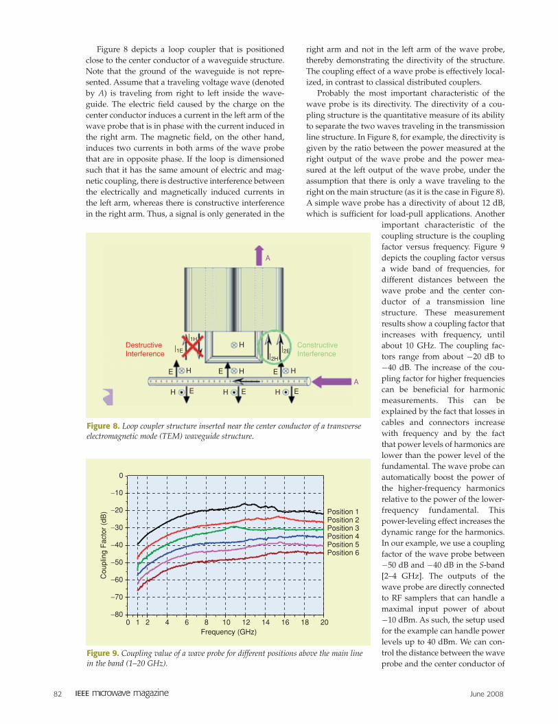
Figure 8 depicts a loop coupler that is positionedclose to the center conductor of a waveguide structure.Note that the ground of the waveguide is not repre-sented. Assume that a traveling voltage wave (denotedby A) is traveling from right to left inside the wave-guide. The electric field caused by the charge on thecenter conductor induces a current in the left arm of thewave probe that is in phase with the current induced inthe right arm. The magnetic field, on the other hand,induces two currents in both arms of the wave probethat are in opposite phase. If the loop is dimensionedsuch that it has the same amount of electric and mag-netic coupling, there is destructive interference betweenthe electrically and magnetically induced currents inthe left arm, whereas there is constructive interferencein the right arm. Thus, a signal is only generated in the
right arm and not in the left arm of the wave probe,thereby demonstrating the directivity of the structure.The coupling effect of a wave probe is effectively local-ized, in contrast to classical distributed couplers.
Probably the most important characteristic of thewave probe is its directivity. The directivity of a cou-pling structure is the quantitative measure of its abilityto separate the two waves traveling in the transmissionline structure. In Figure 8, for example, the directivity isgiven by the ratio between the power measured at theright output of the wave probe and the power mea-sured at the left output of the wave probe, under theassumption that there is only a wave traveling to theright on the main structure (as it is the case in Figure 8).A simple wave probe has a directivity of about 12 dB,which is sufficient for load-pull applications. Another
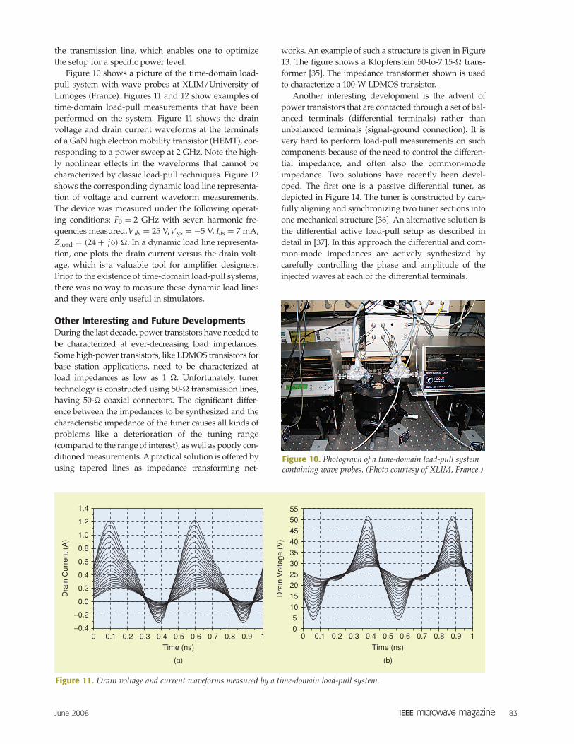
important characteristic of thecoupling structure is the couplingfactor versus frequency. Figure 9depicts the coupling factor versusa wide band of frequencies, fordifferent distances between thewave probe and the center con-ductor of a transmission linestructure. These measurementresults show a coupling factor thatincreases with frequency, untilabout 10 GHz. The coupling fac-tors range from about −20 dB to−40 dB. The increase of the cou-pling factor for higher frequenciescan be beneficial for harmonicmeasurements. This can beexplained by the fact that losses incables and connectors increasewith frequency and by the factthat power levels of harmonics arelower than the power level of thefundamental. The wave probe canautomatically boost the power ofthe higher-frequency harmonicsrelative to the power of the lower-frequency fundamental. Thispower-leveling effect increases thedynamic range for the harmonics.In our example, we use a couplingfactor of the wave probe between−50 dB and −40 dB in the S-band[2–4 GHz]. The outputs of thewave probe are directly connectedto RF samplers that can handle amaximal input power of about−10 dBm. As such, the setup usedfor the example can handle powerlevels up to 40 dBm. We can con-trol the distance between the waveprobe and the center conductor of
Figure 8. Loop coupler structure inserted near the center conductor of a transverseelectromagnetic mode (TEM) waveguide structure.
H
H H
ConstructiveInterference
DestructiveInterference
A
A
H
|1H
|2H
|1E |2E
H H H EEE
E E E
Figure 9. Coupling value of a wave probe for different positions above the main linein the band (1–20 GHz).
Cou
plin
g F
acto
r (d
B)
Frequency (GHz)201816141210864210
−80
−70
−60
−50
−40
−30
−20
−10
0
Position 1Position 2Position 3Position 4Position 5Position 6
June 2008 83
the transmission line, which enables one to optimizethe setup for a specific power level.
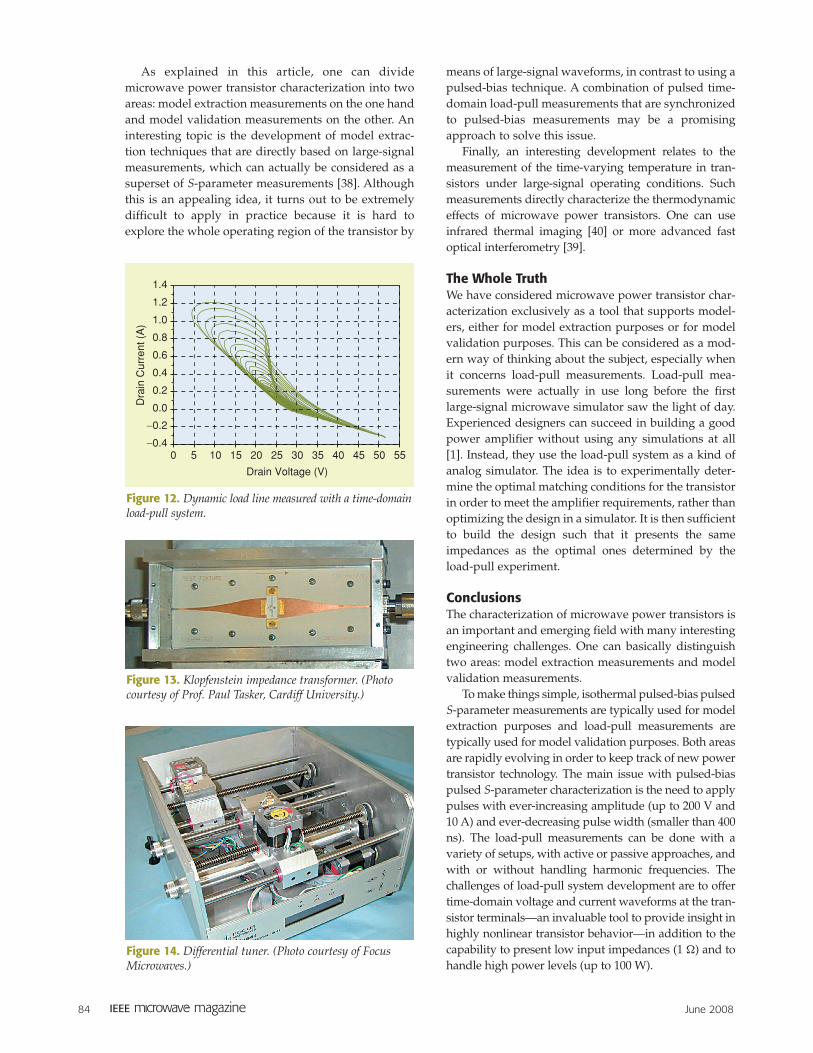
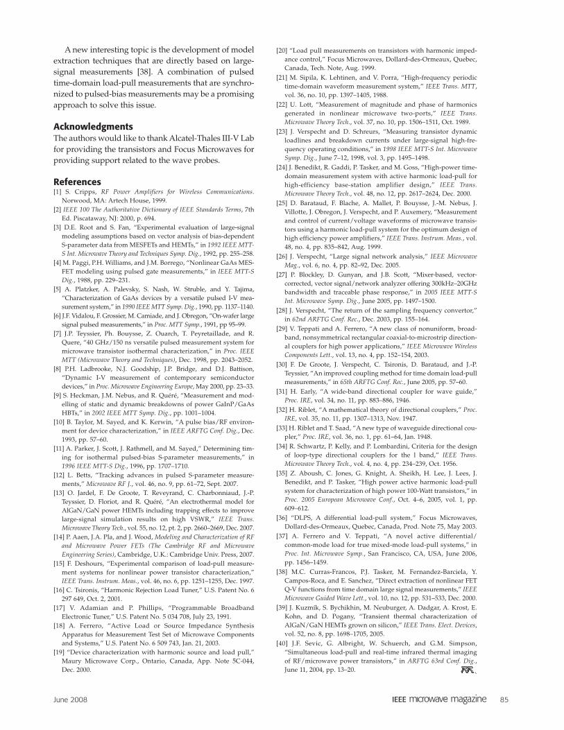
Figure 10 shows a picture of the time-domain load-pull system with wave probes at XLIM/University ofLimoges (France). Figures 11 and 12 show examples oftime-domain load-pull measurements that have beenperformed on the system. Figure 11 shows the drainvoltage and drain current waveforms at the terminalsof a GaN high electron mobility transistor (HEMT), cor-responding to a power sweep at 2 GHz. Note the high-ly nonlinear effects in the waveforms that cannot be characterized by classic load-pull techniques. Figure 12shows the corresponding dynamic load line representa-tion of voltage and current waveform measurements.The device was measured under the following operat-ing conditions: F0 = 2 GHz with seven harmonic fre-quencies measured, Vds = 25 V, Vgs = −5 V, Ids = 7 mA,Zload = (24 + j6) �. In a dynamic load line representa-tion, one plots the drain current versus the drain volt-age, which is a valuable tool for amplifier designers.Prior to the existence of time-domain load-pull systems,there was no way to measure these dynamic load linesand they were only useful in simulators.
Other Interesting and Future DevelopmentsDuring the last decade, power transistors have needed tobe characterized at ever-decreasing load impedances.Some high-power transistors, like LDMOS transistors forbase station applications, need to be characterized atload impedances as low as 1 �. Unfortunately, tunertechnology is constructed using 50-� transmission lines,having 50-� coaxial connectors. The significant differ-ence between the impedances to be synthesized and thecharacteristic impedance of the tuner causes all kinds ofproblems like a deterioration of the tuning range(compared to the range of interest), as well as poorly con-ditioned measurements. A practical solution is offered byusing tapered lines as impedance transforming net-
works. An example of such a structure is given in Figure13. The figure shows a Klopfenstein 50-to-7.15-� trans-former [35]. The impedance transformer shown is usedto characterize a 100-W LDMOS transistor.
Another interesting development is the advent ofpower transistors that are contacted through a set of bal-anced terminals (differential terminals) rather thanunbalanced terminals (signal-ground connection). It isvery hard to perform load-pull measurements on suchcomponents because of the need to control the differen-tial impedance, and often also the common-modeimpedance. Two solutions have recently been devel-oped. The first one is a passive differential tuner, asdepicted in Figure 14. The tuner is constructed by care-fully aligning and synchronizing two tuner sections intoone mechanical structure [36]. An alternative solution isthe differential active load-pull setup as described indetail in [37]. In this approach the differential and com-mon-mode impedances are actively synthesized bycarefully controlling the phase and amplitude of theinjected waves at each of the differential terminals.
Figure 10. Photograph of a time-domain load-pull systemcontaining wave probes. (Photo courtesy of XLIM, France.)
Figure 11. Drain voltage and current waveforms measured by a time-domain load-pull system.
Dra
in C
urre
nt (
A)
−0.4
−0.2
0.0
0.2
0.4
0.6
0.8
1.0
1.2
1.4
0.50.40.30.20.10 0.90.80.7 10.6
Time (ns)
(b)
Time (ns)
(a)
Dra
in V
olta
ge (
V)
0.80.70.60.50.40.30.20.10 10
5
10
15
20
25
30
35
40
45
50
55
0.9
84 June 2008
As explained in this article, one can dividemicrowave power transistor characterization into twoareas: model extraction measurements on the one handand model validation measurements on the other. Aninteresting topic is the development of model extrac-tion techniques that are directly based on large-signalmeasurements, which can actually be considered as asuperset of S-parameter measurements [38]. Althoughthis is an appealing idea, it turns out to be extremelydifficult to apply in practice because it is hard toexplore the whole operating region of the transistor by
means of large-signal waveforms, in contrast to using apulsed-bias technique. A combination of pulsed time-domain load-pull measurements that are synchronizedto pulsed-bias measurements may be a promisingapproach to solve this issue.
Finally, an interesting development relates to themeasurement of the time-varying temperature in tran-sistors under large-signal operating conditions. Suchmeasurements directly characterize the thermodynamiceffects of microwave power transistors. One can useinfrared thermal imaging [40] or more advanced fastoptical interferometry [39].
The Whole TruthWe have considered microwave power transistor char-acterization exclusively as a tool that supports model-ers, either for model extraction purposes or for modelvalidation purposes. This can be considered as a mod-ern way of thinking about the subject, especially whenit concerns load-pull measurements. Load-pull mea-surements were actually in use long before the firstlarge-signal microwave simulator saw the light of day.Experienced designers can succeed in building a goodpower amplifier without using any simulations at all[1]. Instead, they use the load-pull system as a kind ofanalog simulator. The idea is to experimentally deter-mine the optimal matching conditions for the transistorin order to meet the amplifier requirements, rather thanoptimizing the design in a simulator. It is then sufficientto build the design such that it presents the sameimpedances as the optimal ones determined by theload-pull experiment.
ConclusionsThe characterization of microwave power transistors isan important and emerging field with many interestingengineering challenges. One can basically distinguishtwo areas: model extraction measurements and modelvalidation measurements.
To make things simple, isothermal pulsed-bias pulsedS-parameter measurements are typically used for modelextraction purposes and load-pull measurements aretypically used for model validation purposes. Both areasare rapidly evolving in order to keep track of new powertransistor technology. The main issue with pulsed-biaspulsed S-parameter characterization is the need to applypulses with ever-increasing amplitude (up to 200 V and10 A) and ever-decreasing pulse width (smaller than 400ns). The load-pull measurements can be done with avariety of setups, with active or passive approaches, andwith or without handling harmonic frequencies. Thechallenges of load-pull system development are to offertime-domain voltage and current waveforms at the tran-sistor terminals—an invaluable tool to provide insight inhighly nonlinear transistor behavior—in addition to thecapability to present low input impedances (1 �) and tohandle high power levels (up to 100 W).
Figure 13. Klopfenstein impedance transformer. (Photocourtesy of Prof. Paul Tasker, Cardiff University.)
Figure 14. Differential tuner. (Photo courtesy of FocusMicrowaves.)
Figure 12. Dynamic load line measured with a time-domainload-pull system.
Drain Voltage (V)
Dra
in C
urre
nt (
A)
−0.4
−0.2
0.0
0.2
0.4
0.6
0.8
1.0
1.2
1.4
35302520151050 55504540
June 2008 85
A new interesting topic is the development of modelextraction techniques that are directly based on large-signal measurements [38]. A combination of pulsedtime-domain load-pull measurements that are synchro-nized to pulsed-bias measurements may be a promisingapproach to solve this issue.
AcknowledgmentsThe authors would like to thank Alcatel-Thales III-V Labfor providing the transistors and Focus Microwaves forproviding support related to the wave probes.
References[1] S. Cripps, RF Power Amplifiers for Wireless Communications.
Norwood, MA: Artech House, 1999.[2] IEEE 100 The Authoritative Dictionary of IEEE Standards Terms, 7th
Ed. Piscataway, NJ: 2000, p. 694.[3] D.E. Root and S. Fan, “Experimental evaluation of large-signal
modeling assumptions based on vector analysis of bias-dependentS-parameter data from MESFETs and HEMTs,” in 1992 IEEE MTT-S Int. Microwave Theory and Techniques Symp. Dig., 1992, pp. 255–258.
[4] M. Paggi, P.H. Williams, and J.M. Borrego, “Nonlinear GaAs MES-FET modeling using pulsed gate measurements,” in IEEE MTT-SDig., 1988, pp. 229–231.
[5] A. Platzker, A. Palevsky, S. Nash, W. Struble, and Y. Tajima,“Characterization of GaAs devices by a versatile pulsed I-V mea-surement system,” in 1990 IEEE MTT Symp. Dig., 1990, pp. 1137–1140.
[6] J.F. Vidalou, F. Grossier, M. Camiade, and J. Obregon, “On-wafer largesignal pulsed measurements,” in Proc. MTT Symp., 1991, pp 95–99.
[7] J.P. Teyssier, Ph. Bouysse, Z. Ouarch, T. Peyretaillade, and R.Quere, “40 GHz/150 ns versatile pulsed measurement system formicrowave transistor isothermal characterization,” in Proc. IEEEMTT (Microwave Theory and Techniques), Dec. 1998, pp. 2043–2052.
[8] P.H. Ladbrooke, N.J. Goodship, J.P. Bridge, and D.J. Battison,“Dynamic I-V measurement of contemporary semiconductordevices,” in Proc. Microwave Engineering Europe, May 2000, pp. 23–33.
[9] S. Heckman, J.M. Nebus, and R. Quéré, “Measurement and mod-elling of static and dynamic breakdowns of power GaInP/GaAsHBTs,” in 2002 IEEE MTT Symp. Dig., pp. 1001–1004.
[10] B. Taylor, M. Sayed, and K. Kerwin, “A pulse bias/RF environ-ment for device characterization,” in IEEE ARFTG Conf. Dig., Dec.1993, pp. 57–60.
[11] A. Parker, J. Scott, J. Rathmell, and M. Sayed,” Determining tim-ing for isothermal pulsed-bias S-parameter measurements,” in1996 IEEE MTT-S Dig., 1996, pp. 1707–1710.
[12] L. Betts, “Tracking advances in pulsed S-parameter measure-ments,” Microwave RF J., vol. 46, no. 9, pp. 61–72, Sept. 2007.
[13] O. Jardel, F. De Groote, T. Reveyrand, C. Charbonniaud, J.-P.Teyssier, D. Floriot, and R. Quéré, “An electrothermal model forAlGaN/GaN power HEMTs including trapping effects to improvelarge-signal simulation results on high VSWR,” IEEE Trans.Microwave Theory Tech., vol. 55, no. 12, pt. 2, pp. 2660–2669, Dec. 2007.
[14] P. Aaen, J.A. Pla, and J. Wood, Modeling and Characterization of RFand Microwave Power FETs (The Cambridge RF and MicrowaveEngineering Series), Cambridge, U.K.: Cambridge Univ. Press, 2007.
[15] F. Deshours, “Experimental comparison of load-pull measure-ment systems for nonlinear power transistor characterization,”IEEE Trans. Instrum. Meas., vol. 46, no. 6, pp. 1251–1255, Dec. 1997.
[16] C. Tsironis, “Harmonic Rejection Load Tuner,” U.S. Patent No. 6297 649, Oct. 2, 2001.
[17] V. Adamian and P. Phillips, “Programmable BroadbandElectronic Tuner,” U.S. Patent No. 5 034 708, July 23, 1991.
[18] A. Ferrero, “Active Load or Source Impedance SynthesisApparatus for Measurement Test Set of Microwave Componentsand Systems,” U.S. Patent No. 6 509 743, Jan. 21, 2003.
[19] “Device characterization with harmonic source and load pull,”Maury Microwave Corp., Ontario, Canada, App. Note 5C-044,Dec. 2000.
[20] “Load pull measurements on transistors with harmonic imped-ance control,” Focus Microwaves, Dollard-des-Ormeaux, Quebec,Canada, Tech. Note, Aug. 1999.
[21] M. Sipila, K. Lehtinen, and V. Porra, “High-frequency periodictime-domain waveform measurement system,” IEEE Trans. MTT,vol. 36, no. 10, pp. 1397–1405, 1988.
[22] U. Lott, “Measurement of magnitude and phase of harmonicsgenerated in nonlinear microwave two-ports,” IEEE Trans.Microwave Theory Tech., vol. 37, no. 10, pp. 1506–1511, Oct. 1989.
[23] J. Verspecht and D. Schreurs, “Measuring transistor dynamicloadlines and breakdown currents under large-signal high-fre-quency operating conditions,” in 1998 IEEE MTT-S Int. MicrowaveSymp. Dig., June 7–12, 1998, vol. 3, pp. 1495–1498.
[24] J. Benedikt, R. Gaddi, P. Tasker, and M. Goss, “High-power time-domain measurement system with active harmonic load-pull forhigh-efficiency base-station amplifier design,” IEEE Trans.Microwave Theory Tech., vol. 48, no. 12, pp. 2617–2624, Dec. 2000.
[25] D. Barataud, F. Blache, A. Mallet, P. Bouysse, J.-M. Nebus, J.Villotte, J. Obregon, J. Verspecht, and P. Auxemery, “Measurementand control of current/voltage waveforms of microwave transis-tors using a harmonic load-pull system for the optimum design ofhigh efficiency power amplifiers,” IEEE Trans. Instrum. Meas., vol.48, no. 4, pp. 835–842, Aug. 1999.
[26] J. Verspecht, “Large signal network analysis,” IEEE MicrowaveMag., vol. 6, no. 4, pp. 82–92, Dec. 2005.
[27] P. Blockley, D. Gunyan, and J.B. Scott, “Mixer-based, vector-corrected, vector signal/network analyzer offering 300kHz–20GHzbandwidth and traceable phase response,” in 2005 IEEE MTT-SInt. Microwave Symp. Dig., June 2005, pp. 1497–1500.
[28] J. Verspecht, “The return of the sampling frequency convertor,”in 62nd ARFTG Conf. Rec., Dec. 2003, pp. 155–164.
[29] V. Teppati and A. Ferrero, “A new class of nonuniform, broad-band, nonsymmetrical rectangular coaxial-to-microstrip direction-al couplers for high power applications,” IEEE Microwave WirelessComponents Lett., vol. 13, no. 4, pp. 152–154, 2003.
[30] F. De Groote, J. Verspecht, C. Tsironis, D. Barataud, and J.-P.Teyssier, “An improved coupling method for time domain load-pullmeasurements,” in 65th ARFTG Conf. Rec., June 2005, pp. 57–60.
[31] H. Early, “A wide-band directional coupler for wave guide,”Proc. IRE, vol. 34, no. 11, pp. 883–886, 1946.
[32] H. Riblet, “A mathematical theory of directional couplers,” Proc.IRE, vol. 35, no. 11, pp. 1307–1313, Nov. 1947.
[33] H. Riblet and T. Saad, “A new type of waveguide directional cou-pler,” Proc. IRE, vol. 36, no. 1, pp. 61–64, Jan. 1948.
[34] R. Schwartz, P. Kelly, and P. Lombardini, Criteria for the designof loop-type directional couplers for the l band,” IEEE Trans.Microwave Theory Tech., vol. 4, no. 4, pp. 234–239, Oct. 1956.
[35] Z. Aboush, C. Jones, G. Knight, A. Sheikh, H. Lee, J. Lees, J.Benedikt, and P. Tasker, “High power active harmonic load-pullsystem for characterization of high power 100-Watt transistors,” inProc. 2005 European Microwave Conf., Oct. 4–6, 2005, vol. 1, pp.609–612.
[36] “DLPS, A differential load-pull system,” Focus Microwaves,Dollard-des-Ormeaux, Quebec, Canada, Prod. Note 75, May 2003.
[37] A. Ferrero and V. Teppati, “A novel active differential/common-mode load for true mixed-mode load-pull systems,” inProc. Int. Microwave Symp., San Francisco, CA, USA, June 2006, pp. 1456–1459.
[38] M.C. Curras-Francos, P.J. Tasker, M. Fernandez-Barciela, Y.Campos-Roca, and E. Sanchez, “Direct extraction of nonlinear FETQ-V functions from time domain large signal measurements,” IEEEMicrowave Guided Wave Lett., vol. 10, no. 12, pp. 531–533, Dec. 2000.
[39] J. Kuzmík, S. Bychikhin, M. Neuburger, A. Dadgar, A. Krost, E.Kohn, and D. Pogany, “Transient thermal characterization ofAlGaN/GaN HEMTs grown on silicon,” IEEE Trans. Elect. Devices,vol. 52, no. 8, pp. 1698–1705, 2005.
[40] J.F. Sevic, G. Albright, W. Schuerch, and G.M. Simpson,“Simultaneous load-pull and real-time infrared thermal imagingof RF/microwave power transistors,” in ARFTG 63rd Conf. Dig.,June 11, 2004, pp. 13–20.