35
1
| Date post: | 19-Jan-2017 |
| Category: |
Devices & Hardware |
| Upload: | criterion123 |
| View: | 72 times |
| Download: | 1 times |

1
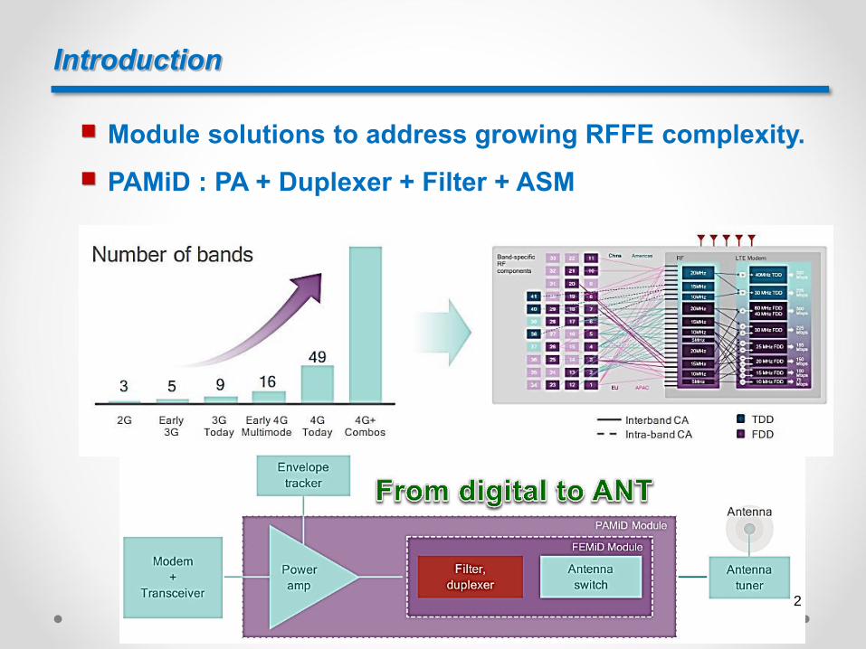
Introduction
Module solutions to address growing RFFE complexity.
PAMiD : PA + Duplexer + Filter + ASM
2
S011
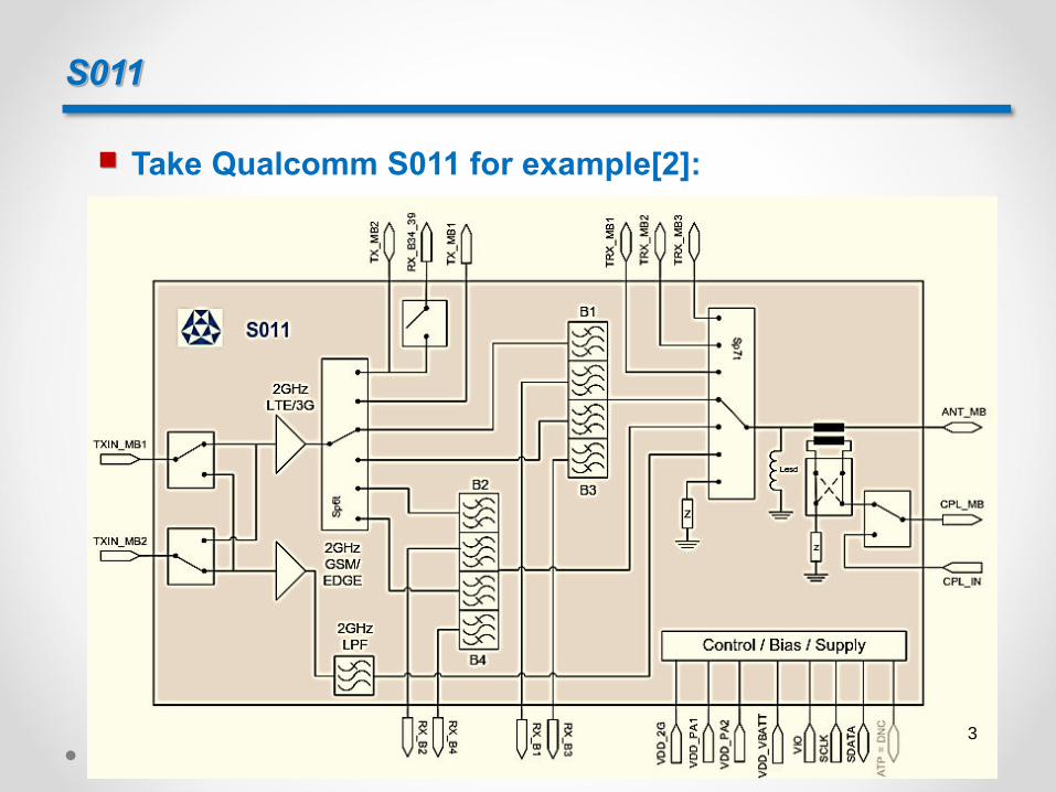
Take Qualcomm S011 for example[2]:
3

S011
Application[2]:
Covering LTE/WCDMA/HSUPA Band 1, 2, 3, 4, DCS, PCS,
Aux Ports
Integration of SAW duplexers, Switches, Envelope Tracking
PA, Coupler
Supporting Inter band Carrier Aggregation Bands 1+3 and
2+4
Single ended in and outputs of all RX ports
4
S011
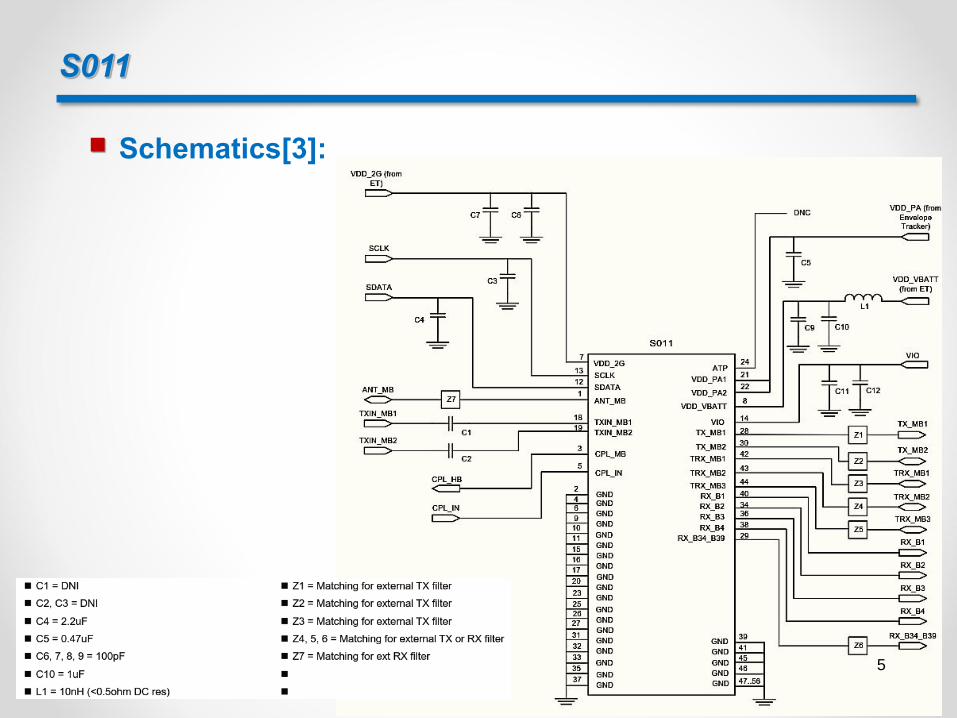
Schematics[3]:
5
S011
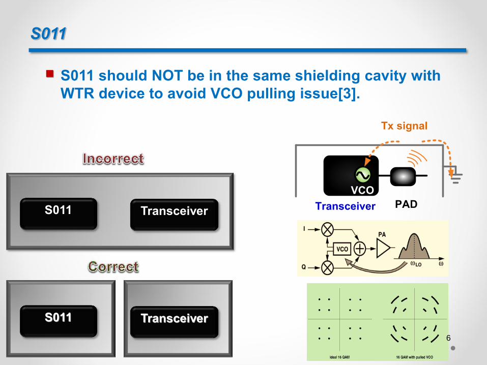
S011 should NOT be in the same shielding cavity with
WTR device to avoid VCO pulling issue[3].
S011 Transceiver
S011 Transceiver
PAD
VCO
Transceiver
Tx signal
6
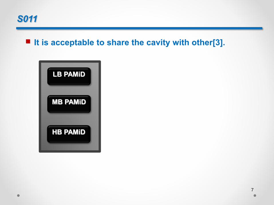
S011
It is acceptable to share the cavity with other[3].
LB PAMiD
MB PAMiD
HB PAMiD
7
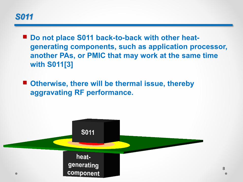
S011
Do not place S011 back-to-back with other heat-
generating components, such as application processor,
another PAs, or PMIC that may work at the same time
with S011[3]
Otherwise, there will be thermal issue, thereby
aggravating RF performance.
8

S011
Top layer layout [3]:
9

S011
With 50 Ohm impedance, the wider the trace width is,
the larger gap between trace and reference GND will be.
The wider the trace width is, the smaller the insertion
loss will be.
Thus, if necessary, cut out can help minimize insertion
loss.
10

S011
But cut out occupies more PCB space.
Besides, according to the calculation, the parasitic
capacitance increases with cut out.
Thus, cut out is a compromise.
3.7 mil 9.5 mil
2.2 mil
5.2 mil
Lengt
11
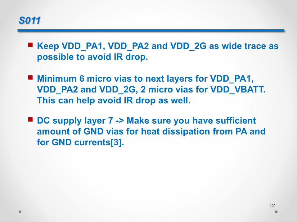
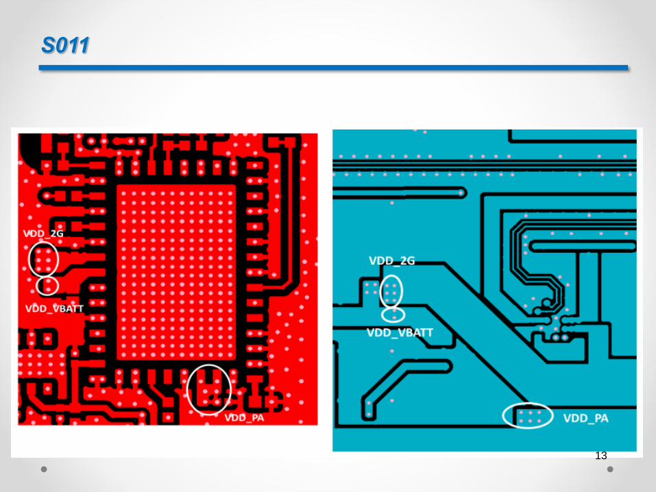
S011
Keep VDD_PA1, VDD_PA2 and VDD_2G as wide trace as
possible to avoid IR drop.
Minimum 6 micro vias to next layers for VDD_PA1,
VDD_PA2 and VDD_2G, 2 micro vias for VDD_VBATT.
This can help avoid IR drop as well.
DC supply layer 7 -> Make sure you have sufficient
amount of GND vias for heat dissipation from PA and
for GND currents[3].
12
S011
13

AFEM-9040 vs. S011 MB PAMid Features
As shown below, in terms of block diagram, the AVAGO
MB PAMiD(AFEM-9040) is the nearly the same as
S011[4].
14
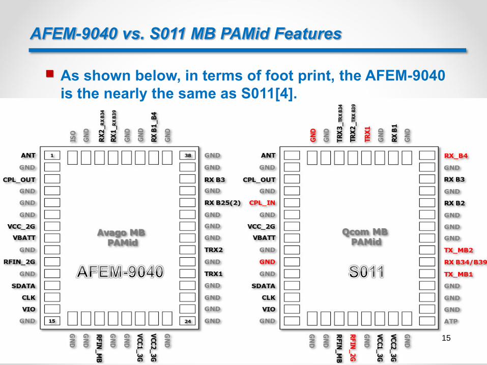
AFEM-9040 vs. S011 MB PAMid Features
As shown below, in terms of foot print, the AFEM-9040
is the nearly the same as S011[4].
15
AFEM-9040 vs. S011 MB PAMid Features
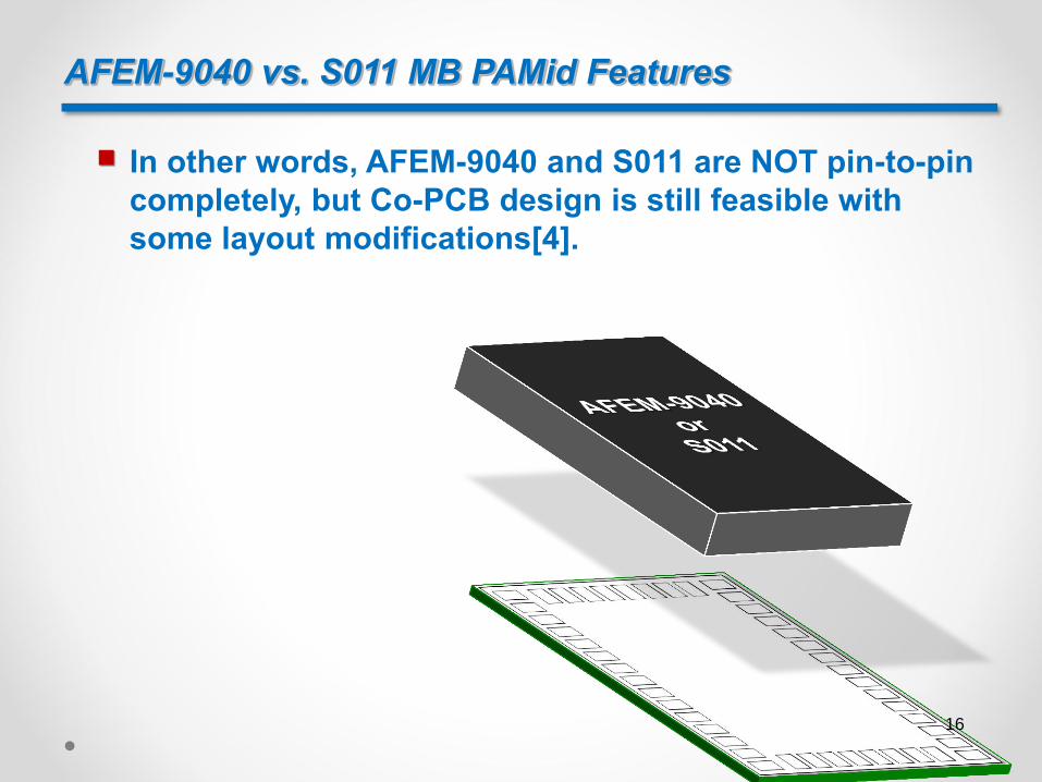
In other words, AFEM-9040 and S011 are NOT pin-to-pin
completely, but Co-PCB design is still feasible with
some layout modifications[4].
16
AFEM-9040 vs. S011 MB PAMid Features
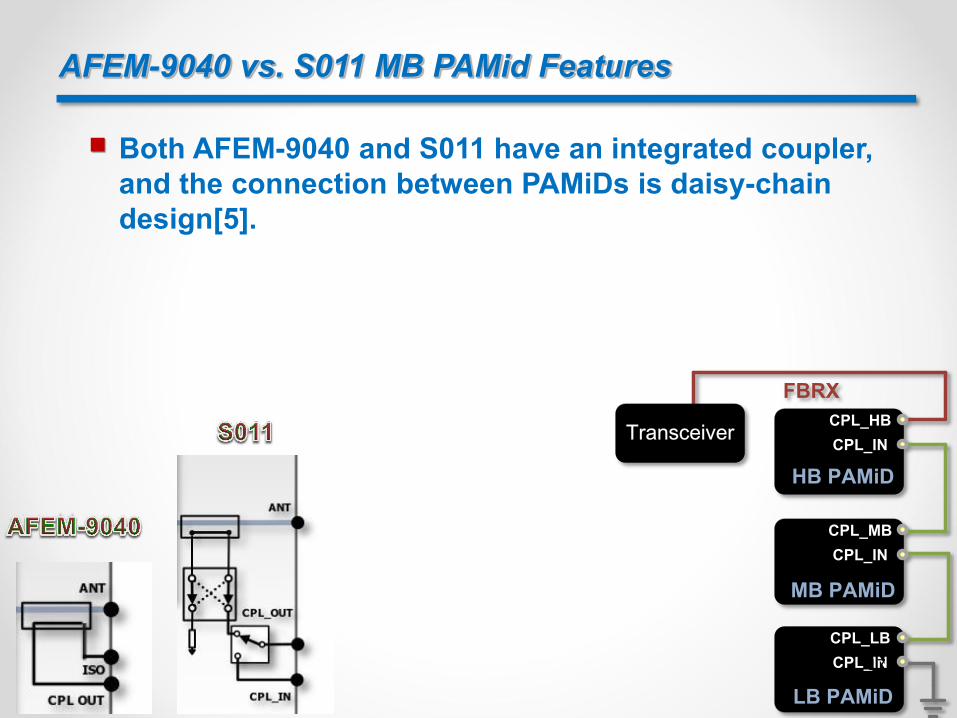
Both AFEM-9040 and S011 have an integrated coupler,
and the connection between PAMiDs is daisy-chain
design[5].
CPL_HB
CPL_IN
CPL_MB
CPL_IN
CPL_LB
CPL_IN
Transceiver
FBRX
HB PAMiD
MB PAMiD
LB PAMiD
17

AFEM-9040 vs. S011 MB PAMid Features
For the pin marked as blue, AFEM-9040 regards it as
isolation pin of integrated coupler; S011 regards it as
GND pin[4].
ANT
GND
GN
D
Thus, for the pin, we need to do some modifications
because of Co-PCB design. AFEM-9040 S011
Blue Pad ISO GND
18
AFEM-9040 vs. S011 MB PAMid Features
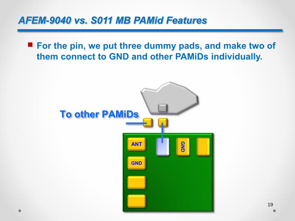
For the pin, we put three dummy pads, and make two of
them connect to GND and other PAMiDs individually.
ANT
GND
GN
DTo other PAMiDs
19
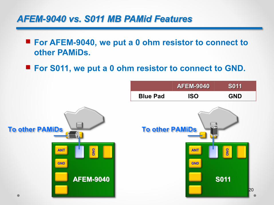
AFEM-9040 vs. S011 MB PAMid Features
For AFEM-9040, we put a 0 ohm resistor to connect to
other PAMiDs.
For S011, we put a 0 ohm resistor to connect to GND.
ANT
GND
GN
D
To other PAMiDs
ANT
GND
GN
D
To other PAMiDs
AFEM-9040 S011
AFEM-9040 S011
Blue Pad ISO GND
20
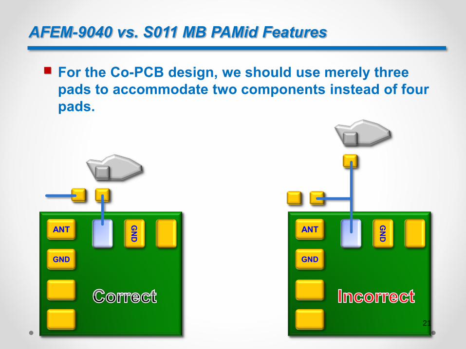
AFEM-9040 vs. S011 MB PAMid Features
For the Co-PCB design, we should use merely three
pads to accommodate two components instead of four
pads.
ANT
GND
GN
D
ANT
GND
GN
D
21
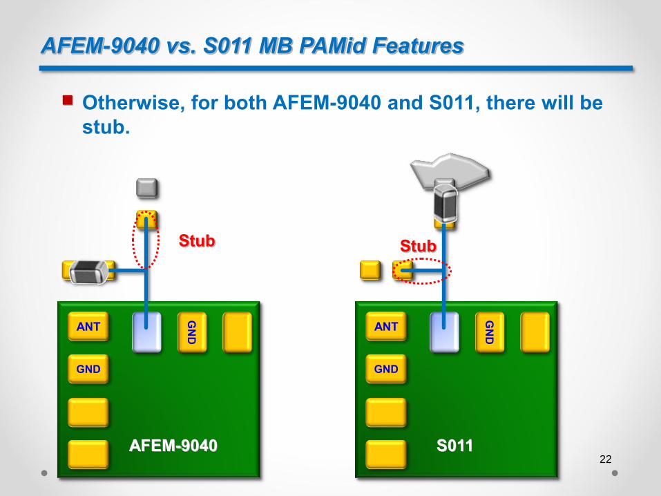
AFEM-9040 vs. S011 MB PAMid Features
Otherwise, for both AFEM-9040 and S011, there will be
stub.
ANT
GND
GN
D
ANT
GND
GN
D
AFEM-9040 S011
Stub Stub
22
AFEM-9040 vs. S011 MB PAMid Features
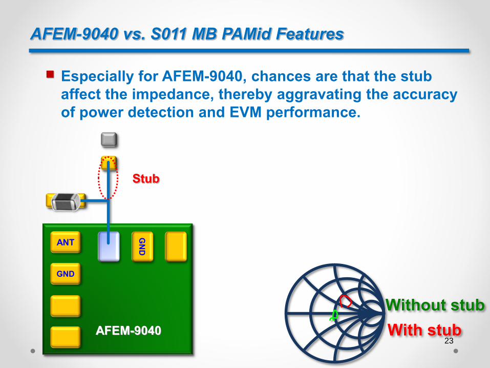
Especially for AFEM-9040, chances are that the stub
affect the impedance, thereby aggravating the accuracy
of power detection and EVM performance.
Without stub
With stub
ANT
GND
GN
D
AFEM-9040
Stub
23

AFEM-9040 vs. S011 MB PAMid Features
Again, for the pin marked as blue, AFEM-9040 regards it
as GND pin; S011 regards it as CPLin pin of integrated
coupler[4].
As mentioned above, put merely three dummy pads.
ANT
GND
CPL
out
GND
ANT
GND
CPL
out
GND
ANT
GND
CPL
out
GND
24
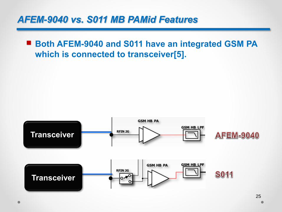
AFEM-9040 vs. S011 MB PAMid Features
Both AFEM-9040 and S011 have an integrated GSM PA
which is connected to transceiver[5].
Transceiver
Transceiver
25
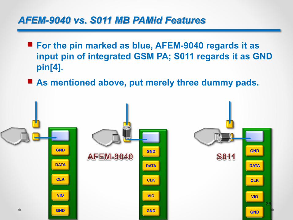
AFEM-9040 vs. S011 MB PAMid Features
For the pin marked as blue, AFEM-9040 regards it as
input pin of integrated GSM PA; S011 regards it as GND
pin[4].
As mentioned above, put merely three dummy pads.
DATA
GND
CLK
VIO
GND
DATA
GND
CLK
VIO
GND
DATA
GND
CLK
VIO
GND
26
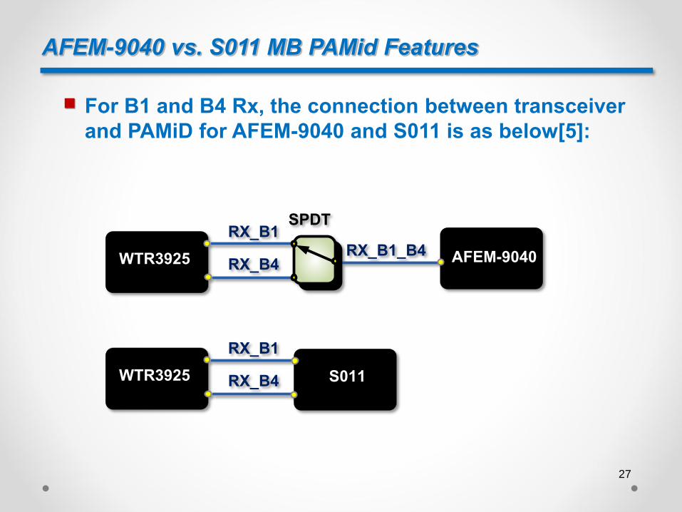
AFEM-9040 vs. S011 MB PAMid Features
For B1 and B4 Rx, the connection between transceiver
and PAMiD for AFEM-9040 and S011 is as below[5]:
RX_B1_B4
SPDT
WTR3925
RX_B1
RX_B4AFEM-9040
WTR3925
RX_B1
RX_B4 S011
27
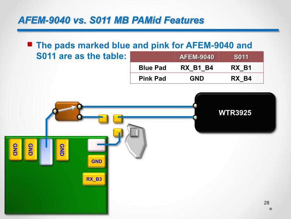
AFEM-9040 vs. S011 MB PAMid Features
The pads marked blue and pink for AFEM-9040 and
S011 are as the table:
AFEM-9040 S011
Blue Pad RX_B1_B4 RX_B1
Pink Pad GND RX_B4
GND
GN
D
GN
D
GN
D
RX_B3
WTR3925
28
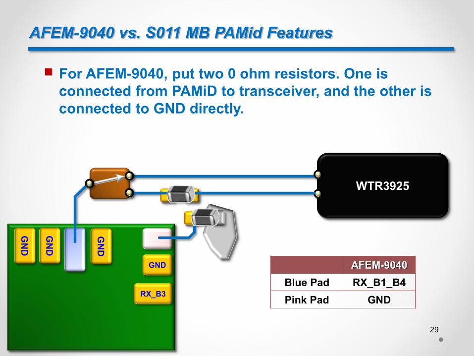
AFEM-9040 vs. S011 MB PAMid Features
For AFEM-9040, put two 0 ohm resistors. One is
connected from PAMiD to transceiver, and the other is
connected to GND directly.
AFEM-9040
Blue Pad RX_B1_B4
Pink Pad GND
GND
GN
D
GN
D
GN
D
RX_B3
WTR3925
29

AFEM-9040 vs. S011 MB PAMid Features
For S011, put merely one 0 ohm resistor that is
connected from PAMiD to transceiver directly.
S011
Blue Pad RX_B1
Pink Pad RX_B4
GND
GN
D
GN
D
GN
D
RX_B3
WTR3925
30

AFEM-9040 vs. S011 MB PAMid Features
For B34 and B39, the connection between transceiver
and PAMiD for AFEM-9040 and S011 is as below[5]:
RX_B34_B39
Diplexer
AFEM-9040
RX_B39
RX_B34 WTR3925
RX_B34_B39
Diplexer
S011 WTR3925
TRX_B34_B39
TRX_B34
TRX_B39
31
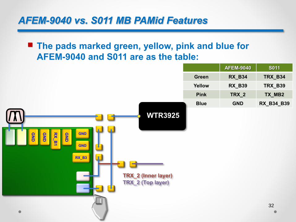
AFEM-9040 vs. S011 MB PAMid Features
The pads marked green, yellow, pink and blue for
AFEM-9040 and S011 are as the table:
AFEM-9040 S011
Green RX_B34 TRX_B34
Yellow RX_B39 TRX_B39
Pink TRX_2 TX_MB2
Blue GND RX_B34_B39
GND
GN
D
RX_B3
GN
D
RX
_B
1
GN
D
GND
WTR3925
TRX_2 (Inner layer)
TRX_2 (Top layer)
32

AFEM-9040 vs. S011 MB PAMid Features
For AFEM-9040, put 3 ohm resistors. The locations of
these 3 ohm resistors are as below :
AFEM-9040
Green RX_B34
Yellow RX_B39
Pink TRX_2
Blue GND
GND
GN
D
RX_B3
GN
D
RX
_B
1
GN
D
GND
WTR3925
TRX_2 (Inner layer)
TRX_2 (Top layer)
33
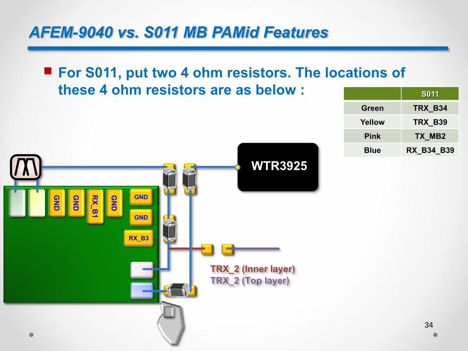
AFEM-9040 vs. S011 MB PAMid Features
For S011, put two 4 ohm resistors. The locations of
these 4 ohm resistors are as below :
GND
GN
D
RX_B3
GN
D
RX
_B
1
GN
D
GND
WTR3925
TRX_2 (Inner layer)
TRX_2 (Top layer)
S011
Green TRX_B34
Yellow TRX_B39
Pink TX_MB2
Blue RX_B34_B39
34
Reference
[1] Qualcomm and TDK Joint Venture, Qualcomm
[2] S011 TDK MB PAMiD Band 1, 2, 3, and 4, Device Specification, Qualcomm
[3] S011 TDK MB PAMID Design Checklist, Qualcomm
[4] Avago PAMid vs. Qcom PAMid, AVAGO
[5] WTR3925 + WTR4905 + Qualcomm RF360™ with HB, MB, and LB PAMiD Global 3DL CA
Design Example, Qualcomm
35


