2168-6777 (c) 2018 IEEE. Personal use is permitted, but republication/redistribution requires IEEE permission. See http://www.ieee.org/publications_standards/publications/rights/index.html for more information. This article has been accepted for publication in a future issue of this journal, but has not been fully edited. Content may change prior to final publication. Citation information: DOI 10.1109/JESTPE.2018.2844376, IEEE Journal of Emerging and Selected Topics in Power Electronics IEEE Journal of Emerging and Selected Topics in Power Electronics Abstract— The SiC MOSFETs are becoming game-changing devices in the field of power electronics, enabling higher temperatures, power densities and efficiencies. However, at higher voltages than 1.7 kV these semiconductors are at early stages of development and yet not commercialized. Based on characterization results of the state-of-the-art 3.3 kV SiC MOSFETs, for the first time this paper investigates design and comparison of topologies commercially used for medium-voltage (MV) drives in 4.16-13.8 kV voltage range in presence of MV SiC MOSFETs. For this purpose, the cascaded H-bridge (CHB), modular multilevel converter (MMC) and five level active neutral point clamped (5-L ANPC) topologies are targeted. Design is carried out at 4.16-, 6.9- and 13.8 kV voltage (4.16- and 6.9 kV in case of 5-L ANPC) and 3- and 5 MVA power ratings using commercial Si IGBTs as well as latest generation non-commercial 3.3 kV SiC MOSFETs, in order to enable investigation of impact from the emerging MV SiC MOSFETs on motor drive system. Selection of several voltage and power levels is to elucidate behavior of converters at different voltage and power rating, and determine the best option for given operating point. Based on design data, comparisons are done among the mentioned topologies from different points of view including efficiency, passive components requirement, semiconductor utilization, power density, low-speed operation capability, fault containment and parts count. Experimental results on an H-bridge cell made with 3.3 kV SiC MOSFETs are brought to verify converter modeling in MATLAB environment as well as the conveyed thermal calculations. Index Terms— Industrial Motor Drives, Si IGBT, SiC MOSFET, Multilevel Converters, Comparison I. INTRODUCTION ULTILEVEL inverters have been the subject of a large number of researches in medium-voltage and high- power applications due to their various advantages such as low common-mode voltages, low dv/dt stresses, low propagated electromagnetic interference (EMI), modularity and high Manuscript received February 16, 2018; revised April 29, 2018 and accepted May 29, 2018. Alinaghi Marzoughi is with EnerSys Delaware Inc., Reading, PA, 19605 USA. Rolando Burgos and Dushan Boroyevich are with the Center for Power Electronics Systems, Bradley Department of Electrical and Computer Engineering, Virginia Polytechnic Institute and State University, Blacksburg, VA, 24061 USA (emails: [email protected]; [email protected]; [email protected]) efficiency [1-3]. Due to the mentioned superiorities, these converters are being used in a vast variety of applications such as industrial drives [4, 5], STATCOM [6], HVDC [7], grid- tied inverter for distributed generation [8], dc-dc power conversion [9] and so on. In the area of industrial motor drives, several multilevel voltage source inverter (VSI) topologies are already being used in commercial products. For low voltage drives, several topologies like the 2-L VSI (e.g. Alstom MV500) and three level neutral point clamped (NPC) converter (e.g. Converteam MV 7000 and Siemens Sinamics SM150) are serving in industry. At higher voltages, the recently patented five level active neutral point clamped (5-L ANPC) topology (used in ACS2000 series by ABB) and the popular cascaded H-bridge (CHB) converter (e.g. Siemens Robicon perfect harmony and Delta Electronics MVD 2000 series) are employed in commercial products. The 5-L ANPC is used by ABB at 4-6.9 kV range, and the CHB converter is the most popular topology in medium voltage range, being commercially manufactured by several vendors for 2.3-13.8 kV drives. Last but not least, the modular multilevel converter (MMC) which is the state-of- the-art topology among multilevel converters has the capability to operate at any given voltage level without any restriction. This converter is already serving in industrial applications such as HVDC, active front-end rectifier for different purposes and motor drive. In the area of comparing multilevel topologies for motor drive application, several efforts have been made so far. In [10] a systematic comparison of four different topologies was shown for direct ac-ac drive of low voltage motors. The converters under study were compared from different points of view such as efficiency and weight (for measure of power density). In [4], neutral point clamped, flying capacitor (FLC) and cascaded H-bridge converters were evaluated to serve as motor drive converter to feed a 4 kV 4.16 MVA motor. Component design, loss calculation and LC filter design were done for the mentioned converter topologies. In a similar fashion to [4], reference [11] compared two-level voltage source converter, three-level NPC, three-level FLC, four-level FLC and five-level CHB converters to realize 2.3 kV 2.4 MVA industrial drive based on 6.5-, 3.3-, and 1.7 kV IGBTs. In [5], the CHB and MMC topologies were compared for motor drive application at medium voltage range. In a similar way later in [12] and [13], the CHB, MMC and 5-L ANPC topologies were designed for medium-voltage drives at Investigating Impact of Emerging Medium- Voltage SiC MOSFETs on Medium-Voltage High-Power Industrial Motor Drives Alinaghi Marzoughi, Student Member, IEEE, Rolando Burgos, Member, IEEE, and Dushan Boroyevich, Fellow Member, IEEE M
Transcript
2168-6777 (c) 2018 IEEE. Personal use is permitted, but republication/redistribution requires IEEE permission. See http://www.ieee.org/publications_standards/publications/rights/index.html for more information.
This article has been accepted for publication in a future issue of this journal, but has not been fully edited. Content may change prior to final publication. Citation information: DOI 10.1109/JESTPE.2018.2844376, IEEE Journalof Emerging and Selected Topics in Power Electronics
IEEE Journal of Emerging and Selected Topics in Power Electronics
Abstract— The SiC MOSFETs are becoming game-changing
devices in the field of power electronics, enabling higher
temperatures, power densities and efficiencies. However, at
higher voltages than 1.7 kV these semiconductors are at early
stages of development and yet not commercialized. Based on
characterization results of the state-of-the-art 3.3 kV SiC
MOSFETs, for the first time this paper investigates design and
comparison of topologies commercially used for medium-voltage
(MV) drives in 4.16-13.8 kV voltage range in presence of MV SiC
MOSFETs. For this purpose, the cascaded H-bridge (CHB),
modular multilevel converter (MMC) and five level active neutral
point clamped (5-L ANPC) topologies are targeted. Design is
carried out at 4.16-, 6.9- and 13.8 kV voltage (4.16- and 6.9 kV in
case of 5-L ANPC) and 3- and 5 MVA power ratings using
commercial Si IGBTs as well as latest generation non-commercial
3.3 kV SiC MOSFETs, in order to enable investigation of impact
from the emerging MV SiC MOSFETs on motor drive system.
Selection of several voltage and power levels is to elucidate
behavior of converters at different voltage and power rating, and
determine the best option for given operating point. Based on
design data, comparisons are done among the mentioned
topologies from different points of view including efficiency,
electromagnetic interference (EMI), modularity and high
Manuscript received February 16, 2018; revised April 29, 2018 and
accepted May 29, 2018. Alinaghi Marzoughi is with EnerSys Delaware Inc., Reading, PA,
19605 USA. Rolando Burgos and Dushan Boroyevich are with the Center for Power Electronics Systems, Bradley Department of Electrical and Computer Engineering, Virginia Polytechnic Institute and State University, Blacksburg, VA, 24061 USA (emails: [email protected]; [email protected]; [email protected])
efficiency [1-3]. Due to the mentioned superiorities, these
converters are being used in a vast variety of applications such
as industrial drives [4, 5], STATCOM [6], HVDC [7], grid-
tied inverter for distributed generation [8], dc-dc power
conversion [9] and so on.
In the area of industrial motor drives, several multilevel
voltage source inverter (VSI) topologies are already being
used in commercial products. For low voltage drives, several
topologies like the 2-L VSI (e.g. Alstom MV500) and three
level neutral point clamped (NPC) converter (e.g. Converteam
MV 7000 and Siemens Sinamics SM150) are serving in
industry. At higher voltages, the recently patented five level
active neutral point clamped (5-L ANPC) topology (used in
ACS2000 series by ABB) and the popular cascaded H-bridge
(CHB) converter (e.g. Siemens Robicon perfect harmony and
Delta Electronics MVD 2000 series) are employed in
commercial products. The 5-L ANPC is used by ABB at 4-6.9
kV range, and the CHB converter is the most popular topology
in medium voltage range, being commercially manufactured
by several vendors for 2.3-13.8 kV drives. Last but not least,
the modular multilevel converter (MMC) which is the state-of-
the-art topology among multilevel converters has the
capability to operate at any given voltage level without any
restriction. This converter is already serving in industrial
applications such as HVDC, active front-end rectifier for
different purposes and motor drive.
In the area of comparing multilevel topologies for motor
drive application, several efforts have been made so far. In
[10] a systematic comparison of four different topologies was
shown for direct ac-ac drive of low voltage motors. The
converters under study were compared from different points of
view such as efficiency and weight (for measure of power
density). In [4], neutral point clamped, flying capacitor (FLC)
and cascaded H-bridge converters were evaluated to serve as
motor drive converter to feed a 4 kV 4.16 MVA motor.
Component design, loss calculation and LC filter design were
done for the mentioned converter topologies. In a similar
fashion to [4], reference [11] compared two-level voltage
2168-6777 (c) 2018 IEEE. Personal use is permitted, but republication/redistribution requires IEEE permission. See http://www.ieee.org/publications_standards/publications/rights/index.html for more information.
This article has been accepted for publication in a future issue of this journal, but has not been fully edited. Content may change prior to final publication. Citation information: DOI 10.1109/JESTPE.2018.2844376, IEEE Journalof Emerging and Selected Topics in Power Electronics
IEEE Journal of Emerging and Selected Topics in Power Electronics
4.16-, 6.9- and 13.8 kV using Si IGBTs, and efficiency, stored
capacitive energy (in J/kVA) and semiconductor utilization of
converters were compared. Last but not least, in [14] the
modular multilevel converter and the triple-star bridge-cell
(TSBC) converter configurations were compared for medium-
voltage drive application under different types of loads.
Since realization of first SiC MOSFET in 1992 [15] and
thanks to their superior material properties such as high
breakdown field, high thermal conductivity and high electron
velocity [16], these semiconductors have become of special
interest to the researchers in the area of physics and power
electronics. Consequently, SiC MOSFETs are commercialized
at voltages up to 1.7 kV with mature technology resulting in
specific on-resistances as low as 4 mΩ.cm2 [17]. However, at
higher voltages these semiconductors are at early stages of
development by a number of companies around the world and
yet are not commercialized. Several non-commercialized SiC-
based prototypes at 3.3 kV up to 15 kV have been reported in
[18-21]. At the same time with development of SiC
semiconductors, several studies have been performed to
investigate the impact of the new semiconductor technology
on different applications including motor drives.
In [22], authors compared 1.2 kV SiC FETs and Si IGBTs
for inverter and dc-dc applications. Reference [23]
characterized and modeled Si and SiC semiconductors for
optimized design of traction inverters. In [24], comparison of
6.5 kV Si IGBT and SiC FETs for medium-voltage power
electronics applications was done. Reference [25] compared
1200 V Si IGBTs and SiC MOSFETs in matrix converter
application, and assessed efficiency and EMI generated by
each technology. System efficiency and leakage current of Si
IGBTs and SiC FETs in variable-frequency drives was
compared in [26], considering different filtering options.
In this paper, a comparison is made between topologies
used for motor drive application in 4.16-13.8 kV voltage
range. For this purpose, the cascaded H-bridge, modular
multilevel converter and five-level active neutral point
clamped converters are designed to realize medium-voltage
high-power industrial drive at 4.16-, 6.9- and 13.8 kV voltages
and 3- and 5 MVA output powers. Design is done at different
voltage and power ratings so that change in different
parameters can be tracked with change in the operating point,
to help selection of best converter for given operating
conditions. Also, the design is performed using existing Si
IGBTs (both low-voltage (LV) and MV Si IGBTs for CHB
and MMC topologies, and MV Si IGBTs for 5-L ANPC
topology as done in industry) as well as the state-of-the-art
non-commercial 3.3 kV SiC MOSFETs (introduced in [27]
and thoroughly characterized in [28]). The study is trying to
find the answer to the following questions: 1- How do the
topologies compare to each other when designed using
commercially-used Si IGBTs? 2- What is the impact of the
emerging medium-voltage SiC MOSFETs on medium-voltage
drives at different operating points? The converters are fed
from a 13.8 kV grid by means of a diode front-end rectifier.
Leakage parameters of the transformer used in rectifier stage
as well as the switching times and deadtimes of
semiconductors are included in converter models developed in
MATLAB environment. In order to have a fair comparison
between semiconductor technologies, the electro-thermal
properties of the semiconductors are interpolated versus
current rating for calculation of the minimum current rating
(die size) device for each converter, while satisfying thermal
criteria. Based on the design data, converters are compared to
each other from different aspects such as efficiency, passive
components, semiconductor utilization (total installed die area
in converter system), power density, low-speed operation,
fault containment and number of parts (for a measure of
reliability). Last but not least, based on experimental results
achieved from an H-bridge cell made using the investigated
3.3 kV SiC MOSFETs, validity of converter modeling and
thermal calculations are verified.
II. CONVERTER DESIGN
A. Inverter Stage Design
The first step in design of motor drive converters is to size
the dc bus. The minimum dc bus voltage required for the
topologies under study can be calculated from (1) and (2)
according to their corresponding output RMS line voltage. An
appropriate percentage of reserve voltage must be considered
as well to guarantee operation of the converters under
transients and also to compensate for voltage drop on stray
impedances and filters (if any used). Reserve dc voltage of
converters used in medium-voltage high-power drive
application is considered from 4% [29] up to 15% [30] in
literature. In this paper based on information from industrial
drive vendors, a 10% reserve voltage is assumed to guarantee
proper operation of the converters.
,2
l ldc CHB
vv (1)
, , 2.dc MMC dc ANPC l lv v v (2)
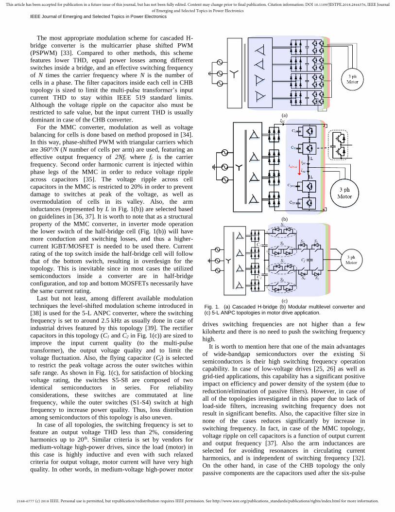
As seen from Fig. 1, full-bridge cells are the building blocks
of the CHB topology [31]. Also, the MMC converter is
composed of half-bridge cells connected in series [32]. In
these modular topologies, the number of cells must be
determined based on the voltage rating of the device used in
the structure. For 1.7- and 3.3 kV semiconductors used in
CHB and MMC topologies, the dc bus is set to be no more
than 1- and 2 kV, respectively, and the number of cells is
selected to satisfy this criteria. This is due to the fact that there
will be a low-frequency ripple on dc bus in case of each
converter (normally about 20% of the nominal voltage), and
the worst-case voltage overshoot assuming switching event at
the peak of capacitor voltage (which is equal to the dc voltage
+ peak ripple value + voltage overshoot of the device at turn-
off) must stay within safe region for the power semiconductor.
On the other hand for the 5-L ANPC converter, in a similar
way to industrial designs, 3.3 kV semiconductors are used at
4.16 kV drives, and 4.5 kV rating IGBTs are employed in
6.9 kV.
2168-6777 (c) 2018 IEEE. Personal use is permitted, but republication/redistribution requires IEEE permission. See http://www.ieee.org/publications_standards/publications/rights/index.html for more information.
This article has been accepted for publication in a future issue of this journal, but has not been fully edited. Content may change prior to final publication. Citation information: DOI 10.1109/JESTPE.2018.2844376, IEEE Journalof Emerging and Selected Topics in Power Electronics
IEEE Journal of Emerging and Selected Topics in Power Electronics
The most appropriate modulation scheme for cascaded H-
bridge converter is the multicarrier phase shifted PWM
(PSPWM) [33]. Compared to other methods, this scheme
features lower THD, equal power losses among different
switches inside a bridge, and an effective switching frequency
of N times the carrier frequency where N is the number of
cells in a phase. The filter capacitors inside each cell in CHB
topology is sized to limit the multi-pulse transformer’s input
current THD to stay within IEEE 519 standard limits.
Although the voltage ripple on the capacitor also must be
restricted to safe value, but the input current THD is usually
dominant in case of the CHB converter.
For the MMC converter, modulation as well as voltage
balancing for cells is done based on method proposed in [34].
In this way, phase-shifted PWM with triangular carriers which
are 360°/N (N number of cells per arm) are used, featuring an
effective output frequency of 2Nfc where fc is the carrier
frequency. Second order harmonic current is injected within
phase legs of the MMC in order to reduce voltage ripple
across capacitors [35]. The voltage ripple across cell
capacitors in the MMC is restricted to 20% in order to prevent
damage to switches at peak of the voltage, as well as
overmodulation of cells in its valley. Also, the arm
inductances (represented by L in Fig. 1(b)) are selected based
on guidelines in [36, 37]. It is worth to note that as a structural
property of the MMC converter, in inverter mode operation
the lower switch of the half-bridge cell (Fig. 1(b)) will have
more conduction and switching losses, and thus a higher-
current IGBT/MOSFET is needed to be used there. Current
rating of the top switch inside the half-bridge cell will follow
that of the bottom switch, resulting in overdesign for the
topology. This is inevitable since in most cases the utilized
semiconductors inside a converter are in half-bridge
configuration, and top and bottom MOSFETs necessarily have
the same current rating.
Last but not least, among different available modulation
techniques the level-shifted modulation scheme introduced in
[38] is used for the 5-L ANPC converter, where the switching
frequency is set to around 2.5 kHz as usually done in case of
industrial drives featured by this topology [39]. The rectifier
capacitors in this topology (C1 and C2 in Fig. 1(c)) are sized to
improve the input current quality (to the multi-pulse
transformer), the output voltage quality and to limit the
voltage fluctuation. Also, the flying capacitor (Cf) is selected
to restrict the peak voltage across the outer switches within
safe range. As shown in Fig. 1(c), for satisfaction of blocking
voltage rating, the switches S5-S8 are composed of two
identical semiconductors in series. For reliability
considerations, these switches are commutated at line
frequency, while the outer switches (S1-S4) switch at high
frequency to increase power quality. Thus, loss distribution
among semiconductors of this topology is also uneven.
In case of all topologies, the switching frequency is set to
feature an output voltage THD less than 2%, considering
harmonics up to 20th. Similar criteria is set by vendors for
medium-voltage high-power drives, since the load (motor) in
this case is highly inductive and even with such relaxed
criteria for output voltage, motor current will have very high
quality. In other words, in medium-voltage high-power motor
drives switching frequencies are not higher than a few
kilohertz and there is no need to push the switching frequency
high.
It is worth to mention here that one of the main advantages
of wide-bandgap semiconductors over the existing Si
semiconductors is their high switching frequency operation
capability. In case of low-voltage drives [25, 26] as well as
grid-tied applications, this capability has a significant positive
impact on efficiency and power density of the system (due to
reduction/elimination of passive filters). However, in case of
all of the topologies investigated in this paper due to lack of
load-side filters, increasing switching frequency does not
result in significant benefits. Also, the capacitive filter size in
none of the cases reduces significantly by increase in
switching frequency. In fact, in case of the MMC topology,
voltage ripple on cell capacitors is a function of output current
and output frequency [37]. Also the arm inductances are
selected for avoiding resonances in circulating current
harmonics, and is independent of switching frequency [32].
On the other hand, in case of the CHB topology the only
passive components are the capacitors used after the six-pulse
(a)
(b)
(c)
Fig. 1. (a) Cascaded H-bridge (b) Modular multilevel converter and (c) 5-L ANPC topologies in motor drive application.
2168-6777 (c) 2018 IEEE. Personal use is permitted, but republication/redistribution requires IEEE permission. See http://www.ieee.org/publications_standards/publications/rights/index.html for more information.
This article has been accepted for publication in a future issue of this journal, but has not been fully edited. Content may change prior to final publication. Citation information: DOI 10.1109/JESTPE.2018.2844376, IEEE Journalof Emerging and Selected Topics in Power Electronics
IEEE Journal of Emerging and Selected Topics in Power Electronics
rectifiers. These capacitors are also independent of inverter
switching frequency. Last but not least, it is shown in [40] that
the main factors contributing to neutral point balance (and
capacitance requirements) in active neutral point clamped
topologies are the load power factor and modulation index.
Since in high modulation indices, the number of possible
switching states (degree of freedom for balancing neutral point
voltage) is not high, increasing switching frequency does not
reduce capacitance requirement in a significant way.
B. Rectifier Stage Design
Six-pulse rectifiers are used together with a multi-pulse
transformer to provide the required dc link for the inverters.
The primary function of the multi-pulse transformer is to
provide galvanic isolation for the rectifiers. Also by using
phase-shifted windings at the transformer’s secondary, it will
be capable of eliminating the input current harmonics and
increasing power quality. According to [30], the blocking
voltage of the individual diodes used in diode front-end
rectifiers must satisfy (3):
2blocking l lv v k (3)
where vl-l is the ac side voltage and k is a safety factor and is
considered to be 2-2.5 for industrial environments. The
leakage impedances of the transformer are also taken into
consideration when designing the rectifier stage and sizing the
capacitive filters. For this purpose, measurement data from
two renown drive manufacturers are used at available voltage
and power ratings. For the rest of the cases, the model derived
in [5] is used to estimate the leakage parameters. It is worth to
mention that the input current to the transformer in all cases
must satisfy IEEE 519 standard [41] for power quality,
restricting THD to 5%.
C. Loss Calculation and Semiconductor Electro-thermal
Properties Interpolation
The method proposed in [42] is used for loss calculation of
diodes and switches at different load currents and
temperatures. In the mentioned technique, the semiconductor
switching and conduction losses are approximated by
polynomials as in (4) and (5). Having the instantaneous
current being conducted/switched, instantaneous losses are
calculated and later integrated to have the average losses over
time. Normally datasheets give switching losses at a constant
dc bus voltage (for instance, 900V dc bus for 1.7 kV IGBTs
and 1.8 kV bus for 3.3 kV IGBTs). If calculation of losses was
needed at a dc bus voltage other than that, the losses were
scaled accordingly as in (6). 2
1 1( ) ( )condP a i t b i t (4)
2
2 2( ) ( )SWP a i t b i t (5)
, ,bus
SW Vbus SW Vref
ref
VE E
V (6)
where i(t) is the instantaneous current, coefficients ai and bi
are derived from loss interpolation according to data from
datasheet, Vbus is the target bus voltage and Vref is the voltage
at which the switching losses are given in datasheet. Having
the semiconductor losses in hand, the average junction
temperature can be calculated from (7). The average junction
temperature of the semiconductors is restricted to 90% of the
maximum possible operating temperature, as normally done
for similar industrial drives.
, ,( )j HS th j c th c h lossT T R R P (7)
where Tj is the junction temperature, THS is the heat sink
temperature, Rth,j-c and Rth,c-h are junction-to-case and case-to-
heat sink thermal resistances respectively, and Ploss is the
average loss of the semiconductor. Finally, heat sinks are
desinged considering a commercial heat sink with cooling
system performance index (CSPI) of 2.48 w/(°C.dm3), and the
heat sink volume is calculated from (8). In this equation the
heat sink temperature is considered to be 80°C and ambient
temperature is 30°C. Also, volume of a fan needed to provide
500 LFM air circulation for the heat sink is considered.
1
.HS amb loss
HS
T T PCSPI Vol
(8)
For design purpose, commercial 1.7 kV Si IGBTs (most
popular semiconductors used by vendors in CHB- and MMC-
based drives) as well as 3.3 kV Si IGBTs (used by Siemens for
some CHB-based drives, and by ABB for 4.16 kV 5-L ANPC
drives) are selected from Infineon products. In case of 6.9 kV
drives based on 5-L ANPC topology, individual
semiconductors need to be rated at 4.5 kV. In a similar way,
4.5 kV IGBTs from Infineon are used for this purpose. Last
but not least, in order to investigate the impact of the emerging
medium-voltage SiC MOSFETs on medium-voltage high-
power drives, the state-of-the-art non-commercial 3.3 kV SiC
MOSFETs from Sumitomo Electric Industries are used [28]. It
is worth to mention that although at the time of this research,
1.7 kV SiC MOSFETs are commercially available from
Wolfspeed, due to much higher conduction losses of
Wolfspeed’s 1.7 kV SiC MOSFETs compared to commercial
1.7 kV Si IGBTs, they do not seem to be a proper option to
use in medium-voltage drive application. Also, as will be
shown later, when using 1.7 kV semiconductors the switching
frequency used for the converters is relatively smaller, where
high switching frequency and low switching loss capabilities
of low-voltage SiC MOSFETs are not beneficial.
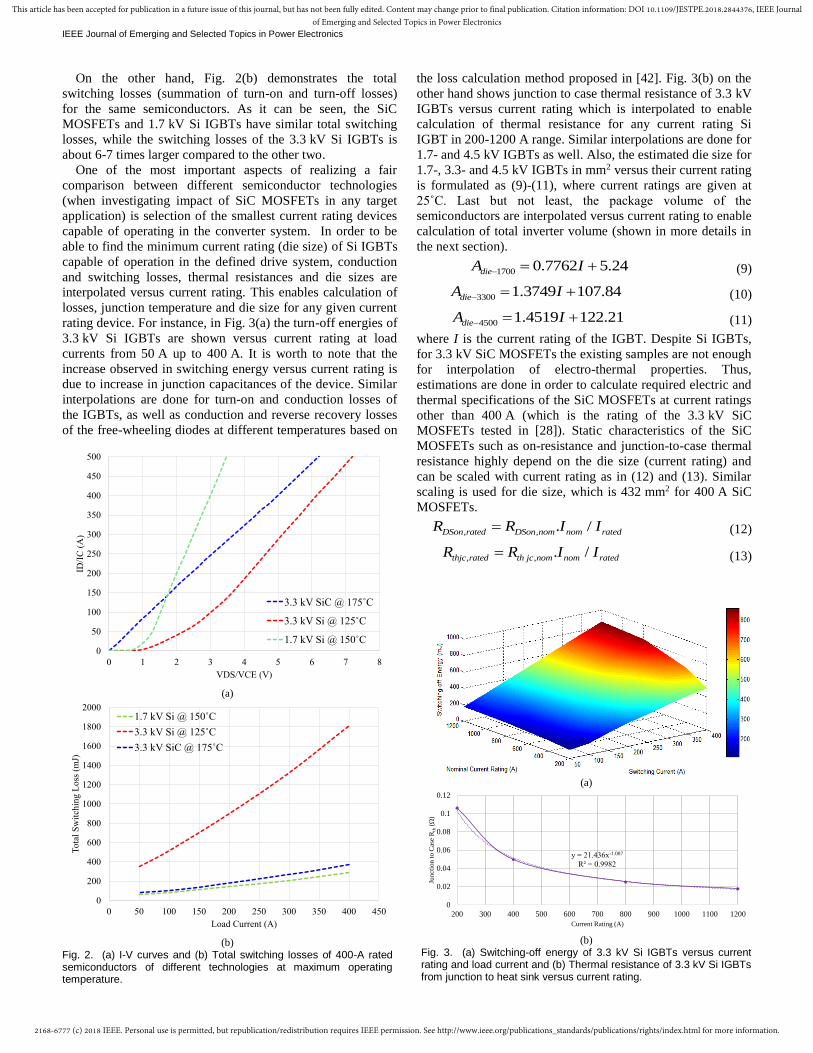
Fig. 2(a) shows the I-V curves for the 1.7 kV IGBTs,
3.3 kV IGBTs and 3.3 kV SiC MOSFETs at 400 A current
rating (current ratings are at 25˚C) to give a measure of
conduction loss, considering that at given load current the
conduction loss would be equal to multiplication of load
current and voltage drop across device terminals. The I-V
curves are given at the maximum junction temperature at
which each semiconductor can operate. As it can be seen, the
3.3 kV SiC MOSFETs feature smaller conduction losses
compared to their Si counterpart for the whole shown load
current interval. Also, the 3.3 kV SiC MOSFETs feature
smaller conduction loss compared to 1.7 kV Si IGBTs up to
around 150 A load current, which is an outstanding feature of
them. Smaller conduction losses of the 3.3 kV SiC MOSFETs
is mainly coming from mature technology of their
manufacturer (Sumitomo Electric Industries), where compared
to other SiC manufacturers, products of Sumitomo Electric
feature smallest specific on-resistance [17].
2168-6777 (c) 2018 IEEE. Personal use is permitted, but republication/redistribution requires IEEE permission. See http://www.ieee.org/publications_standards/publications/rights/index.html for more information.
This article has been accepted for publication in a future issue of this journal, but has not been fully edited. Content may change prior to final publication. Citation information: DOI 10.1109/JESTPE.2018.2844376, IEEE Journalof Emerging and Selected Topics in Power Electronics
IEEE Journal of Emerging and Selected Topics in Power Electronics
On the other hand, Fig. 2(b) demonstrates the total
switching losses (summation of turn-on and turn-off losses)
for the same semiconductors. As it can be seen, the SiC
MOSFETs and 1.7 kV Si IGBTs have similar total switching
losses, while the switching losses of the 3.3 kV Si IGBTs is
about 6-7 times larger compared to the other two.
One of the most important aspects of realizing a fair
comparison between different semiconductor technologies
(when investigating impact of SiC MOSFETs in any target
application) is selection of the smallest current rating devices
capable of operating in the converter system. In order to be
able to find the minimum current rating (die size) of Si IGBTs
capable of operation in the defined drive system, conduction
and switching losses, thermal resistances and die sizes are
interpolated versus current rating. This enables calculation of
losses, junction temperature and die size for any given current
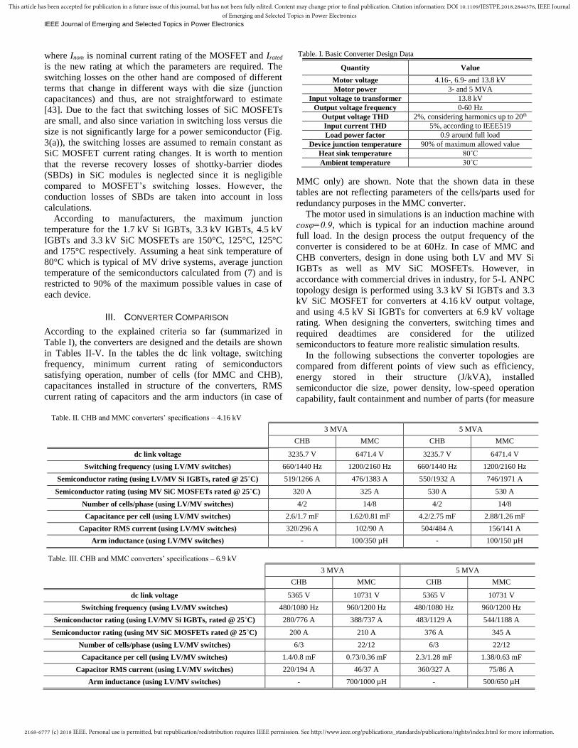
rating device. For instance, in Fig. 3(a) the turn-off energies of
3.3 kV Si IGBTs are shown versus current rating at load
currents from 50 A up to 400 A. It is worth to note that the
increase observed in switching energy versus current rating is
due to increase in junction capacitances of the device. Similar
interpolations are done for turn-on and conduction losses of
the IGBTs, as well as conduction and reverse recovery losses
of the free-wheeling diodes at different temperatures based on
the loss calculation method proposed in [42]. Fig. 3(b) on the
other hand shows junction to case thermal resistance of 3.3 kV
IGBTs versus current rating which is interpolated to enable
calculation of thermal resistance for any current rating Si
IGBT in 200-1200 A range. Similar interpolations are done for
1.7- and 4.5 kV IGBTs as well. Also, the estimated die size for
1.7-, 3.3- and 4.5 kV IGBTs in mm2 versus their current rating
is formulated as (9)-(11), where current ratings are given at
25˚C. Last but not least, the package volume of the
semiconductors are interpolated versus current rating to enable
calculation of total inverter volume (shown in more details in
the next section).
1700 0.7762 5.24dieA I (9)
3300 1.3749 107.84dieA I (10)
4500 1.4519 122.21dieA I (11)
where I is the current rating of the IGBT. Despite Si IGBTs,
for 3.3 kV SiC MOSFETs the existing samples are not enough
for interpolation of electro-thermal properties. Thus,
estimations are done in order to calculate required electric and
thermal specifications of the SiC MOSFETs at current ratings
other than 400 A (which is the rating of the 3.3 kV SiC
MOSFETs tested in [28]). Static characteristics of the SiC
MOSFETs such as on-resistance and junction-to-case thermal
resistance highly depend on the die size (current rating) and
can be scaled with current rating as in (12) and (13). Similar
scaling is used for die size, which is 432 mm2 for 400 A SiC
MOSFETs.
, , . /DSon rated DSon nom nom ratedR R I I (12)
, , . /thjc rated th jc nom nom ratedR R I I (13)
(a)
(b)
Fig. 2. (a) I-V curves and (b) Total switching losses of 400-A rated semiconductors of different technologies at maximum operating temperature.
0
50
100
150
200
250
300
350
400
450
500
0 1 2 3 4 5 6 7 8
ID/I
C (
A)
VDS/VCE (V)
3.3 kV SiC @ 175˚C
3.3 kV Si @ 125˚C
1.7 kV Si @ 150˚C
0
200
400
600
800
1000
1200
1400
1600
1800
2000
0 50 100 150 200 250 300 350 400 450
To
tal
Sw
itch
ing
Lo
ss (
mJ)
Load Current (A)
1.7 kV Si @ 150˚C
3.3 kV Si @ 125˚C
3.3 kV SiC @ 175˚C
(a)
(b)
Fig. 3. (a) Switching-off energy of 3.3 kV Si IGBTs versus current rating and load current and (b) Thermal resistance of 3.3 kV Si IGBTs from junction to heat sink versus current rating.
y = 21.436x-1.007
R² = 0.9982
0
0.02
0.04
0.06
0.08
0.1
0.12
200 300 400 500 600 700 800 900 1000 1100 1200
Jun
ctio
n t
o C
ase
Rth
(Ω)
Current Rating (A)
2168-6777 (c) 2018 IEEE. Personal use is permitted, but republication/redistribution requires IEEE permission. See http://www.ieee.org/publications_standards/publications/rights/index.html for more information.
This article has been accepted for publication in a future issue of this journal, but has not been fully edited. Content may change prior to final publication. Citation information: DOI 10.1109/JESTPE.2018.2844376, IEEE Journalof Emerging and Selected Topics in Power Electronics
IEEE Journal of Emerging and Selected Topics in Power Electronics
Table. I. Basic Converter Design Data
Quantity Value
Motor voltage 4.16-, 6.9- and 13.8 kV
Motor power 3- and 5 MVA
Input voltage to transformer 13.8 kV
Output voltage frequency 0-60 Hz
Output voltage THD 2%, considering harmonics up to 20th
Input current THD 5%, according to IEEE519
Load power factor 0.9 around full load
Device junction temperature 90% of maximum allowed value
Heat sink temperature 80˚C
Ambient temperature 30˚C
Table. II. CHB and MMC converters’ specifications – 4.16 kV
3 MVA 5 MVA
CHB MMC CHB MMC
dc link voltage 3235.7 V 6471.4 V 3235.7 V 6471.4 V
where Inom is nominal current rating of the MOSFET and Irated
is the new rating at which the parameters are required. The
switching losses on the other hand are composed of different
terms that change in different ways with die size (junction
capacitances) and thus, are not straightforward to estimate
[43]. Due to the fact that switching losses of SiC MOSFETs
are small, and also since variation in switching loss versus die
size is not significantly large for a power semiconductor (Fig.
3(a)), the switching losses are assumed to remain constant as
SiC MOSFET current rating changes. It is worth to mention
that the reverse recovery losses of shottky-barrier diodes
(SBDs) in SiC modules is neglected since it is negligible
compared to MOSFET’s switching losses. However, the
conduction losses of SBDs are taken into account in loss
calculations.
According to manufacturers, the maximum junction
temperature for the 1.7 kV Si IGBTs, 3.3 kV IGBTs, 4.5 kV
IGBTs and 3.3 kV SiC MOSFETs are 150°C, 125°C, 125°C
and 175°C respectively. Assuming a heat sink temperature of
80°C which is typical of MV drive systems, average junction
temperature of the semiconductors calculated from (7) and is
restricted to 90% of the maximum possible values in case of
each device.
III. CONVERTER COMPARISON
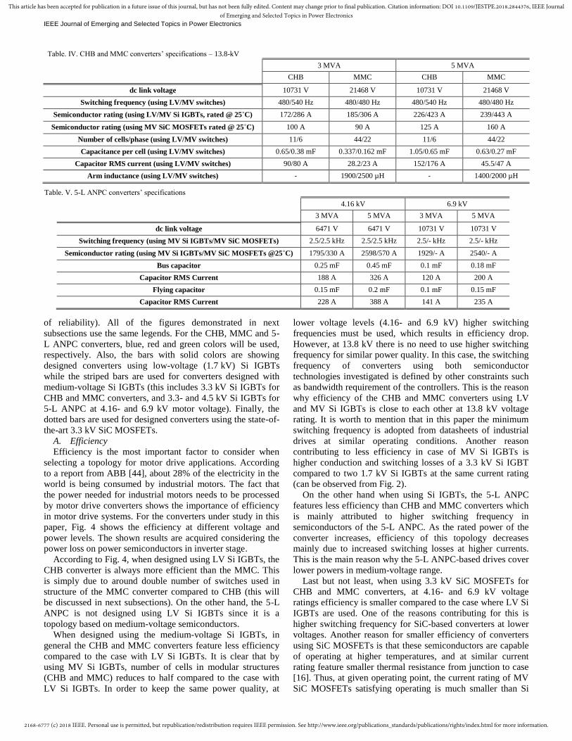
According to the explained criteria so far (summarized in
Table I), the converters are designed and the details are shown
in Tables II-V. In the tables the dc link voltage, switching
frequency, minimum current rating of semiconductors
satisfying operation, number of cells (for MMC and CHB),
capacitances installed in structure of the converters, RMS
current rating of capacitors and the arm inductors (in case of
MMC only) are shown. Note that the shown data in these
tables are not reflecting parameters of the cells/parts used for
redundancy purposes in the MMC converter.
The motor used in simulations is an induction machine with
cosφ=0.9, which is typical for an induction machine around
full load. In the design process the output frequency of the
converter is considered to be at 60Hz. In case of MMC and
CHB converters, design in done using both LV and MV Si
IGBTs as well as MV SiC MOSFETs. However, in
accordance with commercial drives in industry, for 5-L ANPC
topology design is performed using 3.3 kV Si IGBTs and 3.3
kV SiC MOSFET for converters at 4.16 kV output voltage,
and using 4.5 kV Si IGBTs for converters at 6.9 kV voltage
rating. When designing the converters, switching times and
required deadtimes are considered for the utilized
semiconductors to feature more realistic simulation results.
In the following subsections the converter topologies are
compared from different points of view such as efficiency,
energy stored in their structure (J/kVA), installed
semiconductor die size, power density, low-speed operation
capability, fault containment and number of parts (for measure
2168-6777 (c) 2018 IEEE. Personal use is permitted, but republication/redistribution requires IEEE permission. See http://www.ieee.org/publications_standards/publications/rights/index.html for more information.
This article has been accepted for publication in a future issue of this journal, but has not been fully edited. Content may change prior to final publication. Citation information: DOI 10.1109/JESTPE.2018.2844376, IEEE Journalof Emerging and Selected Topics in Power Electronics
IEEE Journal of Emerging and Selected Topics in Power Electronics
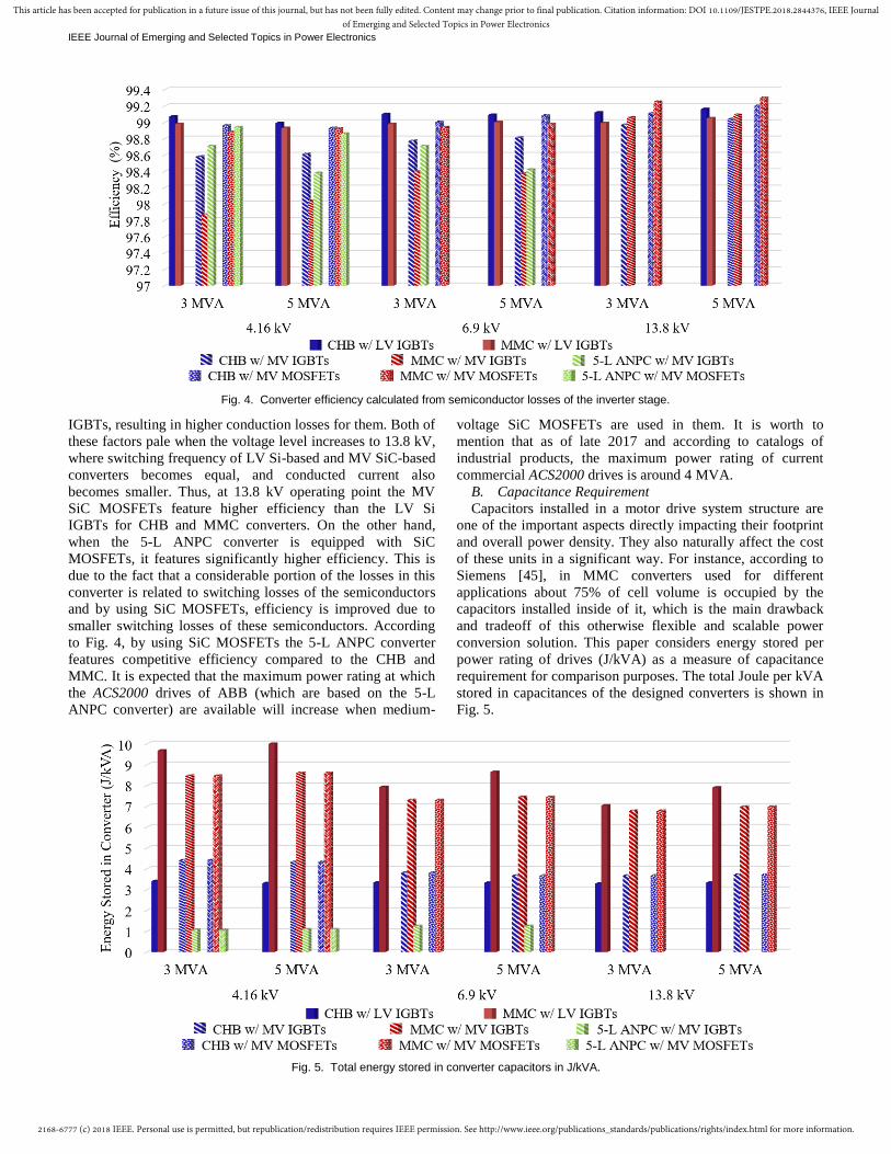
Table. IV. CHB and MMC converters’ specifications – 13.8-kV
Switching frequency (using MV Si IGBTs/MV SiC MOSFETs) 2.5/2.5 kHz 2.5/2.5 kHz 2.5/- kHz 2.5/- kHz
Semiconductor rating (using MV Si IGBTs/MV SiC MOSFETs @25˚C) 1795/330 A 2598/570 A 1929/- A 2540/- A
Bus capacitor 0.25 mF 0.45 mF 0.1 mF 0.18 mF
Capacitor RMS Current 188 A 326 A 120 A 200 A
Flying capacitor 0.15 mF 0.2 mF 0.1 mF 0.15 mF
Capacitor RMS Current 228 A 388 A 141 A 235 A
of reliability). All of the figures demonstrated in next
subsections use the same legends. For the CHB, MMC and 5-
L ANPC converters, blue, red and green colors will be used,
respectively. Also, the bars with solid colors are showing
designed converters using low-voltage (1.7 kV) Si IGBTs
while the striped bars are used for converters designed with
medium-voltage Si IGBTs (this includes 3.3 kV Si IGBTs for
CHB and MMC converters, and 3.3- and 4.5 kV Si IGBTs for
5-L ANPC at 4.16- and 6.9 kV motor voltage). Finally, the
dotted bars are used for designed converters using the state-of-
the-art 3.3 kV SiC MOSFETs.
A. Efficiency
Efficiency is the most important factor to consider when
selecting a topology for motor drive applications. According
to a report from ABB [44], about 28% of the electricity in the
world is being consumed by industrial motors. The fact that
the power needed for industrial motors needs to be processed
by motor drive converters shows the importance of efficiency
in motor drive systems. For the converters under study in this
paper, Fig. 4 shows the efficiency at different voltage and
power levels. The shown results are acquired considering the
power loss on power semiconductors in inverter stage.
According to Fig. 4, when designed using LV Si IGBTs, the
CHB converter is always more efficient than the MMC. This
is simply due to around double number of switches used in
structure of the MMC converter compared to CHB (this will
be discussed in next subsections). On the other hand, the 5-L
ANPC is not designed using LV Si IGBTs since it is a
topology based on medium-voltage semiconductors.
When designed using the medium-voltage Si IGBTs, in
general the CHB and MMC converters feature less efficiency
compared to the case with LV Si IGBTs. It is clear that by
using MV Si IGBTs, number of cells in modular structures
(CHB and MMC) reduces to half compared to the case with
LV Si IGBTs. In order to keep the same power quality, at
lower voltage levels (4.16- and 6.9 kV) higher switching
frequencies must be used, which results in efficiency drop.
However, at 13.8 kV there is no need to use higher switching
frequency for similar power quality. In this case, the switching
frequency of converters using both semiconductor
technologies investigated is defined by other constraints such
as bandwidth requirement of the controllers. This is the reason
why efficiency of the CHB and MMC converters using LV
and MV Si IGBTs is close to each other at 13.8 kV voltage
rating. It is worth to mention that in this paper the minimum
switching frequency is adopted from datasheets of industrial
drives at similar operating conditions. Another reason
contributing to less efficiency in case of MV Si IGBTs is
higher conduction and switching losses of a 3.3 kV Si IGBT
compared to two 1.7 kV Si IGBTs at the same current rating
(can be observed from Fig. 2).
On the other hand when using Si IGBTs, the 5-L ANPC
features less efficiency than CHB and MMC converters which
is mainly attributed to higher switching frequency in
semiconductors of the 5-L ANPC. As the rated power of the
converter increases, efficiency of this topology decreases
mainly due to increased switching losses at higher currents.
This is the main reason why the 5-L ANPC-based drives cover
lower powers in medium-voltage range.
Last but not least, when using 3.3 kV SiC MOSFETs for
CHB and MMC converters, at 4.16- and 6.9 kV voltage
ratings efficiency is smaller compared to the case where LV Si
IGBTs are used. One of the reasons contributing for this is
higher switching frequency for SiC-based converters at lower
voltages. Another reason for smaller efficiency of converters
using SiC MOSFETs is that these semiconductors are capable
of operating at higher temperatures, and at similar current
rating feature smaller thermal resistance from junction to case
[16]. Thus, at given operating point, the current rating of MV
SiC MOSFETs satisfying operating is much smaller than Si
2168-6777 (c) 2018 IEEE. Personal use is permitted, but republication/redistribution requires IEEE permission. See http://www.ieee.org/publications_standards/publications/rights/index.html for more information.
This article has been accepted for publication in a future issue of this journal, but has not been fully edited. Content may change prior to final publication. Citation information: DOI 10.1109/JESTPE.2018.2844376, IEEE Journalof Emerging and Selected Topics in Power Electronics
IEEE Journal of Emerging and Selected Topics in Power Electronics
IGBTs, resulting in higher conduction losses for them. Both of
these factors pale when the voltage level increases to 13.8 kV,
where switching frequency of LV Si-based and MV SiC-based
converters becomes equal, and conducted current also
becomes smaller. Thus, at 13.8 kV operating point the MV
SiC MOSFETs feature higher efficiency than the LV Si
IGBTs for CHB and MMC converters. On the other hand,
when the 5-L ANPC converter is equipped with SiC
MOSFETs, it features significantly higher efficiency. This is
due to the fact that a considerable portion of the losses in this
converter is related to switching losses of the semiconductors
and by using SiC MOSFETs, efficiency is improved due to
smaller switching losses of these semiconductors. According
to Fig. 4, by using SiC MOSFETs the 5-L ANPC converter
features competitive efficiency compared to the CHB and
MMC. It is expected that the maximum power rating at which
the ACS2000 drives of ABB (which are based on the 5-L
ANPC converter) are available will increase when medium-
voltage SiC MOSFETs are used in them. It is worth to
mention that as of late 2017 and according to catalogs of
industrial products, the maximum power rating of current
commercial ACS2000 drives is around 4 MVA.
B. Capacitance Requirement
Capacitors installed in a motor drive system structure are
one of the important aspects directly impacting their footprint
and overall power density. They also naturally affect the cost
of these units in a significant way. For instance, according to
Siemens [45], in MMC converters used for different
applications about 75% of cell volume is occupied by the
capacitors installed inside of it, which is the main drawback
and tradeoff of this otherwise flexible and scalable power
conversion solution. This paper considers energy stored per
power rating of drives (J/kVA) as a measure of capacitance
requirement for comparison purposes. The total Joule per kVA
stored in capacitances of the designed converters is shown in
Fig. 5.
Fig. 4. Converter efficiency calculated from semiconductor losses of the inverter stage.
Fig. 5. Total energy stored in converter capacitors in J/kVA.
2168-6777 (c) 2018 IEEE. Personal use is permitted, but republication/redistribution requires IEEE permission. See http://www.ieee.org/publications_standards/publications/rights/index.html for more information.
This article has been accepted for publication in a future issue of this journal, but has not been fully edited. Content may change prior to final publication. Citation information: DOI 10.1109/JESTPE.2018.2844376, IEEE Journalof Emerging and Selected Topics in Power Electronics
IEEE Journal of Emerging and Selected Topics in Power Electronics
As expected and can be seen from Fig. 5, the capacitance
requirement of the MMC topology is the highest regardless of
the semiconductor type used, which eventually will result in
smaller power density for the converter. On the other hand, the
5-L ANPC topology requires smallest capacitive energy stored
compared to other topologies. Small capacitance requirement
by this topology results in higher power density (discussed in
next subsections), making the 5-L ANPC converter more
attractive. Last but not least, capacitive energy storage of
CHB-based drives is in between those based on MMC and 5-L
ANPC.
It is worth to note that the J/kVA requirement is similar for
converters when either one of the MV semiconductors (Si
IGBTs or SiC MOSFETs) are used. Also when using MV
semiconductors, compared to the case with LV Si IGBTs, the
J/kVA requirement of the MMC converter reduces. This is due
to the fact that the MMC is a nonlinear topology, and by
cutting number of cells in half when MV semiconductors are
used, the arm inductor selected and the corresponding
optimum circulating current that is injected (to reduce
capacitor bank size) changes. On the other side, when MV
semiconductors are used the J/kVA requirement in case of the
CHB converter increases compared to the case with LV Si
IGBTs. According to the aforementioned fact, the capacitors
of the CHB are sized to satisfy IEEE 519 standard at the
multi-pulse transformer’s primary side. When reducing the
number of cells in half, less number of harmonics are
eliminated from transformer’s primary side, resulting in larger
capacitance requirement to compensate for that. The increase
in J/kVA is more obvious in case of 4.16 kV designs, where
by reducing number of H-bridge cells in phase from 4 to 2 by
using MV switches, lower frequency current harmonics are
introduced to the phase current. Since the magnitude of lower-
frequency ripple on capacitor voltage (and on the input current
of the transformer) is higher than the high frequency
harmonics, the increase in capacitance requirement is more
sensible in this case.
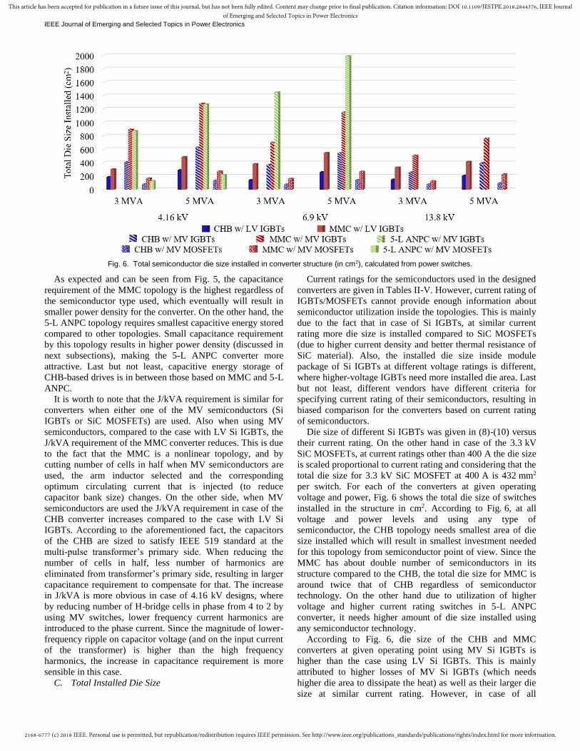
C. Total Installed Die Size
Current ratings for the semiconductors used in the designed
converters are given in Tables II-V. However, current rating of
IGBTs/MOSFETs cannot provide enough information about
semiconductor utilization inside the topologies. This is mainly
due to the fact that in case of Si IGBTs, at similar current
rating more die size is installed compared to SiC MOSFETs
(due to higher current density and better thermal resistance of
SiC material). Also, the installed die size inside module
package of Si IGBTs at different voltage ratings is different,
where higher-voltage IGBTs need more installed die area. Last
but not least, different vendors have different criteria for
specifying current rating of their semiconductors, resulting in
biased comparison for the converters based on current rating
of semiconductors.
Die size of different Si IGBTs was given in (8)-(10) versus
their current rating. On the other hand in case of the 3.3 kV
SiC MOSFETs, at current ratings other than 400 A the die size
is scaled proportional to current rating and considering that the
total die size for 3.3 kV SiC MOSFET at 400 A is 432 mm2
per switch. For each of the converters at given operating
voltage and power, Fig. 6 shows the total die size of switches
installed in the structure in cm2. According to Fig. 6, at all
voltage and power levels and using any type of
semiconductor, the CHB topology needs smallest area of die
size installed which will result in smallest investment needed
for this topology from semiconductor point of view. Since the
MMC has about double number of semiconductors in its
structure compared to the CHB, the total die size for MMC is
around twice that of CHB regardless of semiconductor
technology. On the other hand due to utilization of higher
voltage and higher current rating switches in 5-L ANPC
converter, it needs higher amount of die size installed using
any semiconductor technology.
According to Fig. 6, die size of the CHB and MMC
converters at given operating point using MV Si IGBTs is
higher than the case using LV Si IGBTs. This is mainly
attributed to higher losses of MV Si IGBTs (which needs
higher die area to dissipate the heat) as well as their larger die
size at similar current rating. However, in case of all
Fig. 6. Total semiconductor die size installed in converter structure (in cm2), calculated from power switches.
2168-6777 (c) 2018 IEEE. Personal use is permitted, but republication/redistribution requires IEEE permission. See http://www.ieee.org/publications_standards/publications/rights/index.html for more information.
This article has been accepted for publication in a future issue of this journal, but has not been fully edited. Content may change prior to final publication. Citation information: DOI 10.1109/JESTPE.2018.2844376, IEEE Journalof Emerging and Selected Topics in Power Electronics
IEEE Journal of Emerging and Selected Topics in Power Electronics
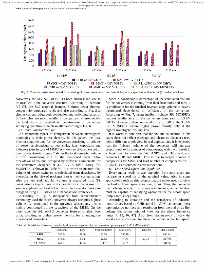
Table. VI. Breakdown of volume occupied by different components for the converters operating at 4.16 kV 5 MVA in dm3.
Heat Sinks Fans Semiconductors Capacitors Inductors Total Volume
CHB 540.54 51.48 10.74 258.18 - 860.94
MMC 549.67 55.2 22.82 741.6 27.73 1397.03
5-L ANPC 443.59 42.24 14.3 84.12 - 584.26
converters, the MV SiC MOSFETs need smallest die size to
be installed in the converter structure. According to literature
[15-17], the SiC material features 3 times better thermal
conductivity compared to Si, and also according to Fig. 2 at
similar current rating both conduction and switching losses of
SiC switches are much smaller in comparison. Consequently,
the total die size installed in the structure of converters
satisfying operating is much smaller according to Fig. 6.
D. Total Inverter Volume
An important aspect of comparison between investigated
topologies is their power density. In this paper, the total
inverter stage volume for the converters consisting of volume
of power semicondcutors, heat sinks, fans, capacitors and
inductors (just in case of MMC) is shown to give a measure of
their power density. Figure 7 shows the total converter volume
in dm3 considering size of the mentioned parts. Also,
breakdown of volume occupied by different components for
the converters designed at 4.16 kV 5 MVA using SiC
MOSFETs is shown in Table VI. It is worth to mention that
volume of power switches is calculated from datasheets, by
interpolating the size of packages versus their current rating.
Also the heat sink and fan volume is measured from (8),
considering a typical heat sink characteristics that is used for
similar applications. Last but not least, the capacitor banks are
designed using FFLI series of Film capacitors from AVX.
According to Fig. 7, independent from semicondcutor
technology used the MMC converter always occupies highest
volume. As mentioned in the previous subsections, this is
mainly contributed by the capacitors of the MMC. On the
other side, the 5-L ANPC converter features smallest foot
print, resulting in highest power density for it among the
investigated converters.
Since a considerable percentage of the calculated volume
for the converters is coming from their heat sinks and fans, it
is predictable for the finished inverter stage volume to have a
meaningful dependency on efficiency of the converters.
According to Fig. 7, using medium voltage SiC MOSFETs
features smaller size for the converters compared to 3.3 kV
IGBTs. However, when compared to LV Si IGBTs, the 3.3 kV
SiC MOSFETs feature higher power density only at the
highest investigated voltage level.
It is worth to note here that the volume calculation in this
paper does not reflect creepage and clearance distances used
within different topologies. In real applications, it is expected
that the finished volume of the converter will increase
proportional to its number of components, which will result in
a larger gap between the 5-L ANPC and CHB, and also
between CHB and MMC. This is due to largest number of
components for MMC and least number of components for 5-
L ANPC, as discussed in next subsections.
E. Low-Speed Operation Capability
Every motor needs to start operation from zero speed and
increase its speed up to the nominal value. Also in some
applications such as ship propulsion, the motor needs to drive
the load at lower speeds for long times. Thus, the converter
that is being selected for driving a motor in given application
must be capable of satisfying operation for the whole speed
(output frequency) range.
According to literature and the datasheets of industrial
motor drives based on CHB and 5-L ANPC converters, these
topologies do not face any restriction from thermal or dc link
voltage fluctuation point of view for the whole frequency
range [4, 12, 46, 47]. Also, from design point of view the
worst case to consider for these converters is the full speed.
Fig. 7. Total converter volume in dm3 consisting of power semiconductors, heat sinks, fans, capacitors and inductor (if used any) volume.
2168-6777 (c) 2018 IEEE. Personal use is permitted, but republication/redistribution requires IEEE permission. See http://www.ieee.org/publications_standards/publications/rights/index.html for more information.
This article has been accepted for publication in a future issue of this journal, but has not been fully edited. Content may change prior to final publication. Citation information: DOI 10.1109/JESTPE.2018.2844376, IEEE Journalof Emerging and Selected Topics in Power Electronics
IEEE Journal of Emerging and Selected Topics in Power Electronics
However, it has been well addressed in several studies that the
MMC converter faces restrictions at lower speeds when used
with high-torque loads [48, 49]. According to (14), the voltage
ripple on capacitors of the MMC changes in opposite direction
with the output frequency of the converter (speed of the
motor) [50]. When used to drive loads with constant (or high)
torque demand at lower speeds, since the output current stays
high (or constant, in case of loads that need constant torque at
lower speeds) the ripple increases as speed reduces. However,
it is shown in [48] that for some loads such as fans, blowers
and centrifugal pumps, since the output torque (phase current)
also reduces with reduction in speed, the converter can operate
at lower frequencies without any problem.
ph
C
IU
C
(14)
where Iph is the phase current of the motor, ω is output angular
frequency, ΔUC is the peak-to-peak ripple and C is capacitance
per phase. Injection of high frequency circulating currents is
proposed as a solution for solving the high ripple problem at
lower frequencies [49], but due to high switching frequency
requirement and significant amount of losses created, it can
only work for short amount of time (startup) rather than
continuous operation at lower frequencies.
F. Fault Containment
The industrial motors are playing a vital role in the
environment that they are being used, and in some
applications they are operating non-stop for long times. Since
failure in operation of the converter driving a motor can stop
the motor from rotating, fault-tolerant operation capability is
one of the important aspects in comparison of topologies.
Faults can be introduced to the converters due to failure in
semiconductors, fans, passive components as well as
communication/control units.
According to datasheets of CHB-based drives, if failure
happens inside a cell within the converter, the cell will be
bypassed and the converter can continue to operate with de-
rated output voltage. In this case by modifying the phase
angles of the phase voltages of the converter with respect to
each other, symmetrical line voltages can be achieved for the
motor. Magnitude of the line voltage with one cell bypassed in
one of the phases can be calculated from (15).
,
2 1
2l l new l l
nv v
n
(15)
where n is number of cells per phase and vl-l is the nominal
line voltage of the converter. On the other hand, for the MMC
converter auxiliary cells are usually placed within the
converter phase legs, so that in case of failure in a cell it can
be bypassed and an auxiliary cell can start working instead.
This will guarantee uninterrupted operation of the converter
without any reduction in the output voltage. However, despite
the modular structures discussed in this paper the 5-L ANPC
converter does not feature fault-tolerant operation. If one of
the semiconductors or its corresponding gate
driver/communication fails, operation of the whole converter
will be interrupted.
G. Number of Components
Inherent reliability of a converter system is a function of the
number of component used in it. In other words, parts count is
the most straightforward method to assess reliability in a
system, given the associated higher probability of failure that
results from a higher number of system components. A
discussion on the reliability of different voltage rating Si or
SiC semiconductors is beyond the scope of this paper
however, for which the number of semiconductors will be
used to compare reliability between the converters under
study.
Among the converters designed and with respect to Tables
II-V, the 5-L ANPC requires the least number of
semiconductors. In both 4.16- and 6.9 kV voltage levels, this
converter needs 12 IGBT/diode modules per phase (resulting
in 36 total for three phases). However, this number for CHB at
4.16- and 6.9 kV is 48 and 72, and for MMC it is 84 and 132,
respectively. At 13.8 kV a similar ratio exists among the
number of switches for MMC and CHB. At this voltage level,
MMC needs 264 IGBT/diode pairs, while for operation of
CHB 132 pairs are enough. In other words, MMC converter at
all voltage and power levels needs highest number of power
switches. This is another main drawback of MMC converter,
affecting its reliability. It is also clear that the number of gate
drivers, communication fibers and etc. in the converters will
be equal to number of their semiconductors, which adds more
to reliability concerns of converters with high number of
switches.
On the other hand since CHB converter needs separated dc
link voltages, number of front-end rectifier diodes in it will be
higher than that of MMC and 5-L ANPC. Number of diodes
used in front-end rectifiers of CHB converter is simply 6 times
the number of cells in converter. Thus, for 4.16-, 6.9- and 13.8
kV CHB converters designed in this paper, 72, 108 and 198
rectifier diodes are needed while at the same voltage levels for
MMC and 5-L ANPC only 24 diodes are required. Although
presspack diodes (which are normally used for DFE stage of
medium-voltage drives) are highly reliable and when failing,
they are normally shorted (so they do not interfere operation
of the converter, if additional diodes are placed in series when
designing) but number of diodes is proportional to number of
secondary windings in multi-pulse transformer used with
drives. Number of transformer secondary windings in CHB
converter is equal to the number of H-bridge cells used. Thus,
CHB converter has a more complicated transformer.
As the voltage level increases, CHB requires more and
more secondary windings and finally at 13.8 kV, it needs 33
secondary windings on transformer. Large number of
secondary windings adds to the complexity of transformer
design and implementation, potentially increasing its cost.
Also, due to utilization of more insulating material within the
converter structure, its size also increases. This is the main
reason why some vendors such as Siemens use 3.3 kV Si
IGBTs for very high voltage drive systems, resulting in cost
reduction of the transformer. It is worth to note that for MMC
and 5-L ANPC converters, a total of 4 secondary windings is
enough for operation of the converter at any voltage and
power level. This number of secondary windings is selected to
satisfy IEEE 519 at the primary side without using any
additional filters.
2168-6777 (c) 2018 IEEE. Personal use is permitted, but republication/redistribution requires IEEE permission. See http://www.ieee.org/publications_standards/publications/rights/index.html for more information.
This article has been accepted for publication in a future issue of this journal, but has not been fully edited. Content may change prior to final publication. Citation information: DOI 10.1109/JESTPE.2018.2844376, IEEE Journalof Emerging and Selected Topics in Power Electronics
IEEE Journal of Emerging and Selected Topics in Power Electronics
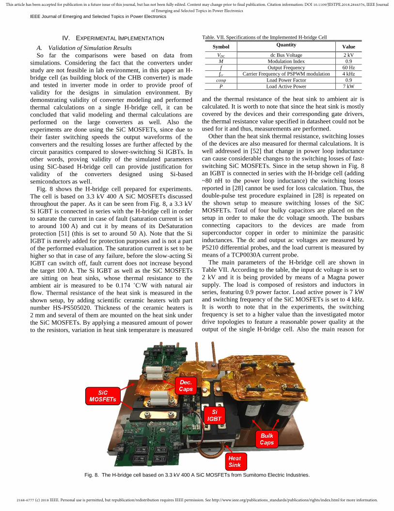
Table. VII. Specifications of the Implemented H-bridge Cell
Symbol Quantity Value
VDC dc Bus Voltage 2 kV
M Modulation Index 0.9
f Output Frequency 60 Hz
fcr Carrier Frequency of PSPWM modulation 4 kHz
cosφ Load Power Factor 0.9
P Load Active Power 7 kW
IV. EXPERIMENTAL IMPLEMENTATION
A. Validation of Simulation Results
So far the comparisons were based on data from
simulations. Considering the fact that the converters under
study are not feasible in lab environment, in this paper an H-
bridge cell (as building block of the CHB converter) is made
and tested in inverter mode in order to provide proof of
validity for the designs in simulation environment. By
demonstrating validity of converter modeling and performed
thermal calculations on a single H-bridge cell, it can be
concluded that valid modeling and thermal calculations are
performed on the large converters as well. Also the
experiments are done using the SiC MOSFETs, since due to
their faster switching speeds the output waveforms of the
converters and the resulting losses are further affected by the
circuit parasitics compared to slower-switching Si IGBTs. In
other words, proving validity of the simulated parameters
using SiC-based H-bridge cell can provide justification for
validity of the converters designed using Si-based
semiconductors as well.
Fig. 8 shows the H-bridge cell prepared for experiments.
The cell is based on 3.3 kV 400 A SiC MOSFETs discussed
throughout the paper. As it can be seen from Fig. 8, a 3.3 kV
Si IGBT is connected in series with the H-bridge cell in order
to saturate the current in case of fault (saturation current is set
to around 100 A) and cut it by means of its DeSaturation
protection [51] (this is set to around 50 A). Note that the Si
IGBT is merely added for protection purposes and is not a part
of the performed evaluation. The saturation current is set to be
higher so that in case of any failure, before the slow-acting Si
IGBT can switch off, fault current does not increase beyond
the target 100 A. The Si IGBT as well as the SiC MOSFETs
are sitting on heat sinks, whose thermal resistance to the
ambient air is measured to be 0.174 ˚C/W with natural air
flow. Thermal resistance of the heat sink is measured in the
shown setup, by adding scientific ceramic heaters with part
number HS-PS505020. Thickness of the ceramic heaters is
2 mm and several of them are mounted on the heat sink under
the SiC MOSFETs. By applying a measured amount of power
to the resistors, variation in heat sink temperature is measured
and the thermal resistance of the heat sink to ambient air is
calculated. It is worth to note that since the heat sink is mostly
covered by the devices and their corresponding gate drivers,
the thermal resistance value specified in datasheet could not be
used for it and thus, measurements are performed.
Other than the heat sink thermal resistance, switching losses
of the devices are also measured for thermal calculations. It is
well addressed in [52] that change in power loop inductance
can cause considerable changes to the switching losses of fast-
switching SiC MOSFETs. Since in the setup shown in Fig. 8
an IGBT is connected in series with the H-bridge cell (adding
~80 nH to the power loop inductance) the switching losses
reported in [28] cannot be used for loss calculation. Thus, the
double-pulse test procedure explained in [28] is repeated on
the shown setup to measure switching losses of the SiC
MOSFETs. Total of four bulky capacitors are placed on the
setup in order to make the dc voltage smooth. The busbars
connecting capacitors to the devices are made from
superconductor copper in order to minimize the parasitic
inductances. The dc and output ac voltages are measured by
P5210 differential probes, and the load current is measured by
means of a TCP0030A current probe.
The main parameters of the H-bridge cell are shown in
Table VII. According to the table, the input dc voltage is set to
2 kV and it is being provided by means of a Magna power
supply. The load is composed of resistors and inductors in
series, featuring 0.9 power factor. Load active power is 7 kW
and switching frequency of the SiC MOSFETs is set to 4 kHz.
It is worth to note that in the experiments, the switching
frequency is set to a higher value than the investigated motor
drive topologies to feature a reasonable power quality at the
output of the single H-bridge cell. Also the main reason for
Fig. 8. The H-bridge cell based on 3.3 kV 400 A SiC MOSFETs from Sumitomo Electric Industries.
2168-6777 (c) 2018 IEEE. Personal use is permitted, but republication/redistribution requires IEEE permission. See http://www.ieee.org/publications_standards/publications/rights/index.html for more information.
This article has been accepted for publication in a future issue of this journal, but has not been fully edited. Content may change prior to final publication. Citation information: DOI 10.1109/JESTPE.2018.2844376, IEEE Journalof Emerging and Selected Topics in Power Electronics
IEEE Journal of Emerging and Selected Topics in Power Electronics
restriction of operating power to 7 kW is lack of high-power
load banks with high-voltage (>2 kV) operation capability.
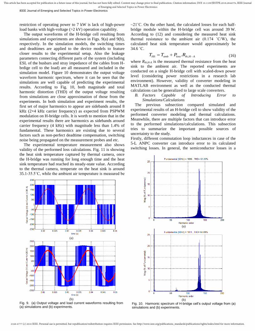
The output waveforms of the H-bridge cell resulting from
simulations and experiments are shown in Figs. 9(a) and 9(b),
respectively. In the simulation models, the switching times
and deadtimes are applied to the device models to feature
closer results to the experimental setup. Also the leakage
parameters connecting different parts of the system (including
ESL of the busbars and stray impedance of the cables from H-
brdige cell to the load) are all measured and included in the
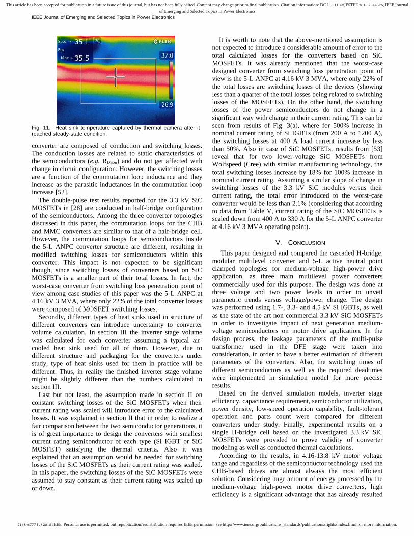
simulation model. Figure 10 demonstrates the output voltage
waveform harmonic spectrum, where it can be seen that the
simulations are well capable of predicting the experimental
results. According to Fig. 10, both magnitude and total
harmonic distortion (THD) of the output voltage resulting
from simulations are close approximation of those from the
experiments. In both simulation and experiment results, the
first set of major harmonics to appear are sidebands around 8
kHz (2×4 kHz carrier frequency) as expected from PSPWM
modulation on H-bridge cells. It is worth to mention that in the
experimental results there are harmonics as sidebands around
carrier frequency (4 kHz) with magnitude less than 1.4% of
fundamental. These harmonics are existing due to several
factors such as non-perfect deadtime compensation, switching
noise being propagated on the measurement probes and etc.
The experimental temperature measurement also shows
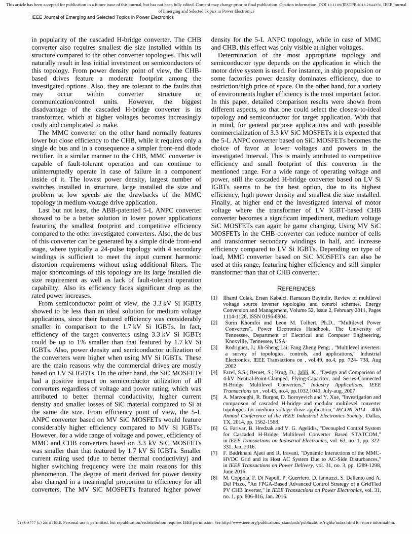
validity of the performed loss calculations. Fig. 11 is showing
the heat sink temperature captured by thermal camera, once
the H-bridge was running for long enough time and the heat
sink temperature had reached its steady-state value. According
to the thermal camera, temperate on the heat sink is around
35.1-35.5˚C, while the ambient air temperature is measured be
~21˚C. On the other hand, the calculated losses for each half-
bridge module within the H-bridge cell was around 39 W.
According to (12) and considering the measured heat sink
thermal resistance to the ambient air (0.174 ˚C/W), the
calculated heat sink temperature would approximately be
34.6 ˚C.
,.HS amb loss th H AT T P R (16)
where Rth,H-A is the measured thermal resistance from the heat
sink to the ambient air. The reported experiments are
conducted on a single H-bridge cell with scaled-down power
level (considering power restrictions in a research lab
environment). However, validity of converter modeling in
MATLAB environment as well as the conducted thermal
calculations can be generalized to large scale converters.
B. Factors Capable of Introducing Error to
Simulations/Calculations
The previous subsection compared simulated and
experimental results of an H-bridge cell to show validity of the
performed converter modeling and thermal calculations.
Meanwhile, there are multiple factors that can introduce error
to the performed simulations/calculations. This subsection
tries to summarize the important possible sources of
uncertainty to the study.
Firstly, different commutation loop inductances in case of the
5-L ANPC converter can introduce error to its calculated
switching losses. In general, the semiconductor losses in a
(a)
(b)
Fig. 9. (a) Output voltage and load current waveforms resulting from (a) simulations and (b) experiments.
(a)
(b)
Fig. 10. Harmonic spectrum of H-bridge cell’s output voltage from (a) simulations and (b) experiments.
2168-6777 (c) 2018 IEEE. Personal use is permitted, but republication/redistribution requires IEEE permission. See http://www.ieee.org/publications_standards/publications/rights/index.html for more information.
This article has been accepted for publication in a future issue of this journal, but has not been fully edited. Content may change prior to final publication. Citation information: DOI 10.1109/JESTPE.2018.2844376, IEEE Journalof Emerging and Selected Topics in Power Electronics
IEEE Journal of Emerging and Selected Topics in Power Electronics
converter are composed of conduction and switching losses.
The conduction losses are related to static characteristics of
the semiconductors (e.g. RDSon) and do not get affected with
change in circuit configuration. However, the switching losses
are a function of the commutation loop inductance and they
increase as the parasitic inductances in the commutation loop
increase [52].
The double-pulse test results reported for the 3.3 kV SiC
MOSFETs in [28] are conducted in half-bridge configuration
of the semiconductors. Among the three converter topologies
discussed in this paper, the commutation loops for the CHB
and MMC converters are similar to that of a half-bridge cell.
However, the commutation loops for semiconductors inside
the 5-L ANPC converter structure are different, resulting in
modified switching losses for semiconductors within this
converter. This impact is not expected to be significant
though, since switching losses of converters based on SiC
MOSFETs is a smaller part of their total losses. In fact, the
worst-case converter from switching loss penetration point of
view among case studies of this paper was the 5-L ANPC at
4.16 kV 3 MVA, where only 22% of the total converter losses
were composed of MOSFET switching losses.
Secondly, different types of heat sinks used in structure of
different converters can introduce uncertainty to converter
volume calculation. In section III the inverter stage volume
was calculated for each converter assuming a typical air-
cooled heat sink used for all of them. However, due to
different structure and packaging for the converters under
study, type of heat sinks used for them in practice will be
different. Thus, in reality the finished inverter stage volume
might be slightly different than the numbers calculated in
section III.
Last but not least, the assumption made in section II on
constant switching losses of the SiC MOSFETs when their
current rating was scaled will introduce error to the calculated
losses. It was explained in section II that in order to realize a
fair comparison between the two semiconductor generations, it
is of great importance to design the converters with smallest
current rating semiconductor of each type (Si IGBT or SiC
MOSFET) satisfying the thermal criteria. Also it was
explained that an assumption would be needed for switching
losses of the SiC MOSFETs as their current rating was scaled.
In this paper, the switching losses of the SiC MOSFETs were
assumed to stay constant as their current rating was scaled up
or down.
It is worth to note that the above-mentioned assumption is
not expected to introduce a considerable amount of error to the
total calculated losses for the converters based on SiC
MOSFETs. It was already mentioned that the worst-case
designed converter from switching loss penetration point of
view is the 5-L ANPC at 4.16 kV 3 MVA, where only 22% of
the total losses are switching losses of the devices (showing
less than a quarter of the total losses being related to switching
losses of the MOSFETs). On the other hand, the switching
losses of the power semiconductors do not change in a
significant way with change in their current rating. This can be
seen from results of Fig. 3(a), where for 500% increase in
nominal current rating of Si IGBTs (from 200 A to 1200 A),
the switching losses at 400 A load current increase by less
than 50%. Also in case of SiC MOSFETs, results from [53]
reveal that for two lower-voltage SiC MOSFETs from
Wolfspeed (Cree) with similar manufacturing technology, the
total switching losses increase by 18% for 100% increase in
nominal current rating. Assuming a similar slope of change in
switching losses of the 3.3 kV SiC modules versus their
current rating, the total error introduced to the worst-case
converter would be less than 2.1% (considering that according
to data from Table V, current rating of the SiC MOSFETs is
scaled down from 400 A to 330 A for the 5-L ANPC converter
at 4.16 kV 3 MVA operating point).
V. CONCLUSION
This paper designed and compared the cascaded H-bridge,
modular multilevel converter and 5-L active neutral point
clamped topologies for medium-voltage high-power drive
application, as three main multilevel power converters
commercially used for this purpose. The design was done at
three voltage and two power levels in order to unveil
parametric trends versus voltage/power change. The design
was performed using 1.7-, 3.3- and 4.5 kV Si IGBTs, as well
as the state-of-the-art non-commercial 3.3 kV SiC MOSFETs
in order to investigate impact of next generation medium-
voltage semiconductors on motor drive application. In the
design process, the leakage parameters of the multi-pulse
transformer used in the DFE stage were taken into
consideration, in order to have a better estimation of different
parameters of the converters. Also, the switching times of
different semiconductors as well as the required deadtimes
were implemented in simulation model for more precise
results.
Based on the derived simulation models, inverter stage
power density, low-speed operation capability, fault-tolerant
operation and parts count were compared for different
converters under study. Finally, experimental results on a
single H-bridge cell based on the investigated 3.3 kV SiC
MOSFETs were provided to prove validity of converter
modeling as well as conducted thermal calculations.
According to the results, in 4.16-13.8 kV motor voltage
range and regardless of the semiconductor technology used the
CHB-based drives are almost always the most efficient
solution. Considering huge amount of energy processed by the
medium-voltage high-power motor drive converters, high
efficiency is a significant advantage that has already resulted
Fig. 11. Heat sink temperature captured by thermal camera after it reached steady-state condition.
2168-6777 (c) 2018 IEEE. Personal use is permitted, but republication/redistribution requires IEEE permission. See http://www.ieee.org/publications_standards/publications/rights/index.html for more information.
This article has been accepted for publication in a future issue of this journal, but has not been fully edited. Content may change prior to final publication. Citation information: DOI 10.1109/JESTPE.2018.2844376, IEEE Journalof Emerging and Selected Topics in Power Electronics
IEEE Journal of Emerging and Selected Topics in Power Electronics
in popularity of the cascaded H-bridge converter. The CHB
converter also requires smallest die size installed within its
structure compared to the other converter topologies. This will
naturally result in less initial investment on semiconductors of
this topology. From power density point of view, the CHB-
based drives feature a moderate footprint among the
investigated options. Also, they are tolerant to the faults that
may occur within converter structure or
communication/control units. However, the biggest
disadvantage of the cascaded H-bridge converter is its
transformer, which at higher voltages becomes increasingly
costly and complicated to make.
The MMC converter on the other hand normally features
lower but close efficiency to the CHB, while it requires only a
single dc bus and in a consequence a simpler front-end diode
rectifier. In a similar manner to the CHB, MMC converter is
capable of fault-tolerant operation and can continue to
uninterruptedly operate in case of failure in a component
inside of it. The lowest power density, largest number of
switches installed in structure, large installed die size and
problem at low speeds are the drawbacks of the MMC
topology in medium-voltage drive application.
Last but not least, the ABB-patented 5-L ANPC converter
showed to be a better solution in lower power applications
featuring the smallest footprint and competitive efficiency
compared to the other investigated converters. Also, the dc bus
of this converter can be generated by a simple diode front-end
stage, where typically a 24-pulse topology with 4 secondary
windings is sufficient to meet the input current harmonic
distortion requirements without using additional filters. The
major shortcomings of this topology are its large installed die
size requirement as well as lack of fault-tolerant operation
capability. Also its efficiency faces significant drop as the
rated power increases.
From semiconductor point of view, the 3.3 kV Si IGBTs
showed to be less than an ideal solution for medium voltage
applications, since their featured efficiency was considerably
smaller in comparison to the 1.7 kV Si IGBTs. In fact,
efficiency of the target converters using 3.3 kV Si IGBTs
could be up to 1% smaller than that featured by 1.7 kV Si
IGBTs. Also, power density and semiconductor utilization of
the converters were higher when using MV Si IGBTs. These
are the main reasons why the commercial drives are mostly
based on LV Si IGBTs. On the other hand, the SiC MOSFETs
had a positive impact on semiconductor utilization of all
converters regardless of voltage and power rating, which was
attributed to better thermal conductivity, higher current
density and smaller losses of SiC material compared to Si at
the same die size. From efficiency point of view, the 5-L
ANPC converter based on MV SiC MOSFETs would feature
considerably higher efficiency compared to MV Si IGBTs.
However, for a wide range of voltage and power, efficiency of
MMC and CHB converters based on 3.3 kV SiC MOSFETs
was smaller than that featured by 1.7 kV Si IGBTs. Smaller
current rating used (due to better thermal conductivity) and
higher switching frequency were the main reasons for this
phenomenon. The degree of merit derived for power density
also changed in a meaningful proportion to efficiency for all
converters. The MV SiC MOSFETs featured higher power
density for the 5-L ANPC topology, while in case of MMC
and CHB, this effect was only visible at higher voltages.
Determination of the most appropriate topology and
semiconductor type depends on the application in which the
motor drive system is used. For instance, in ship propulsion or
some factories power density dominates efficiency, due to
restriction/high price of space. On the other hand, for a variety
of environments higher efficiency is the most important factor.
In this paper, detailed comparison results were shown from
different aspects, so that one could select the closest-to-ideal
topology and semiconductor for target application. With that
in mind, for general purpose applications and with possible
commercialization of 3.3 kV SiC MOSFETs it is expected that
the 5-L ANPC converter based on SiC MOSFETs becomes the
choice of favor at lower voltages and powers in the
investigated interval. This is mainly attributed to competitive
efficiency and small footprint of this converter in the
mentioned range. For a wide range of operating voltage and
power, still the cascaded H-bridge converter based on LV Si
IGBTs seems to be the best option, due to its highest
efficiency, high power density and smallest die size installed.
Finally, at higher end of the investigated interval of motor
voltage where the transformer of LV IGBT-based CHB
converter becomes a significant impediment, medium voltage
SiC MOSFETs can again be game changing. Using MV SiC
MOSFETs in the CHB converter can reduce number of cells
and transformer secondary windings in half, and increase
efficiency compared to LV Si IGBTs. Depending on type of
load, MMC converter based on SiC MOSFETs can also be
used at this range, featuring higher efficiency and still simpler
transformer than that of CHB converter.
REFERENCES
[1] Ilhami Colak, Ersan Kabalci, Ramazan Bayindir, Review of multilevel voltage source inverter topologies and control schemes, Energy
Conversion and Management, Volume 52, Issue 2, February 2011, Pages
1114-1128, ISSN 0196-8904. [2] Surin Khomfoi and Leon M. Tolbert, Ph.D., “Multilevel Power
Converters”, Power Electronics Handbook, The University of
Tennessee, Department of Electrical and Computer Engineering, Knoxville, Tennessee, USA
2168-6777 (c) 2018 IEEE. Personal use is permitted, but republication/redistribution requires IEEE permission. See http://www.ieee.org/publications_standards/publications/rights/index.html for more information.
This article has been accepted for publication in a future issue of this journal, but has not been fully edited. Content may change prior to final publication. Citation information: DOI 10.1109/JESTPE.2018.2844376, IEEE Journalof Emerging and Selected Topics in Power Electronics
IEEE Journal of Emerging and Selected Topics in Power Electronics
[9] A. A. Taffese, E. Tedeschi and E. C. W. de Jong, "Modelling of DC-DC
converters based on front-to-front connected MMC for small signal studies," 2016 IEEE 17th Workshop on Control and Modeling for Power
Electronics (COMPEL), Trondheim, 2016, pp. 1-7.
[10] R. Lai et al., "A Systematic Topology Evaluation Methodology for High-Density Three-Phase PWM AC-AC Converters," in IEEE
Transactions on Power Electronics, vol. 23, no. 6, pp. 2665-2680, Nov.
2168-6777 (c) 2018 IEEE. Personal use is permitted, but republication/redistribution requires IEEE permission. See http://www.ieee.org/publications_standards/publications/rights/index.html for more information.
This article has been accepted for publication in a future issue of this journal, but has not been fully edited. Content may change prior to final publication. Citation information: DOI 10.1109/JESTPE.2018.2844376, IEEE Journalof Emerging and Selected Topics in Power Electronics
IEEE Journal of Emerging and Selected Topics in Power Electronics
[48] Hagiwara, M.; Nishimura, K.; Akagi, H., "A Medium-Voltage Motor
Drive With a Modular Multilevel PWM Inverter," Power Electronics, IEEE Transactions on , vol.25, no.7, pp.1786,1799, July 2010
[49] A. J. Korn, M. Winkelnkemper and P. Steimer, "Low output frequency
operation of the Modular Multi-Level Converter," 2010 IEEE Energy Conversion Congress and Exposition, Atlanta, GA, 2010, pp. 3993-
3997.
[50] Marzoughi, A.; Burgos, RP.; Boroyevich, D.; Xue, Y., "Steady-State Analysis of Voltages and Currents in Modular Multilevel Converter
Based on Average Model," Energy Conversion Congress and
Exposition (ECCE) 2015 [51] J. Rice and J. Mookken, "SiC MOSFET gate drive design
considerations," Integrated Power Packaging (IWIPP), 2015 IEEE International Workshop on, Chicago, IL, 2015, pp. 24-27.
[52] Z. Chen, “Characterization and Modeling of High-Switching-Speed
Behavior of SiC Active Devices,” M.S. thesis, Department of Electrical and Computer Engineering, Virginia Tech, Blacksburg, Virginia, 2009.
[53] A. Marzoughi, A. Romero, R. Burgos and D. Boroyevich, "Comparing
the State-of-the-Art SiC MOSFETs: Test results reveal characteristics of four major manufacturers’ 900-V and 1.2-kV SiC devices," in IEEE
Power Electronics Magazine, vol. 4, no. 2, pp. 36-45, June 2017
Alinaghi Marzoughi (S’14) received B.S. and M.S. degrees in electrical engineering from University of Tehran, Tehran, Iran in 2010 and 2013, respectively. In 2013, he joined the Center for Power Electronics Systems (CPES), Virginia Tech and completed his Ph.D. program in 2017. He is currently with Enersys as Systems Integration Manager. His research interests include power electronic converter modeling and control, wide-bandgap semiconductors and grid
interface for renewable energy and energy storage systems. Rolando Burgos (S’96–M’03) received the B.S. on Electronics
Engineering, the Electronics Engineering Professional Degree, and the M.S. and Ph.D. degrees in Electrical Engineering from the University of Concepción, Chile, in 1995, 1997, 1999, and 2002 respectively. In 2002 he joined, as Postdoctoral Fellow, the Center for Power Electronics Systems (CPES) at Virginia Tech, in Blacksburg, VA, becoming Research Scientist in 2003, and Research Assistant Professor in 2005. In 2009 he joined ABB Corporate Research in
Raleigh, NC, where he was Scientist (2009–2010), and Principal Scientist (2010–2012). In 2010 he was appointed Adjunct Associate Professor in the Electrical and Computer Engineering Department at North Carolina State University at the Future Renewable Electric Energy Delivery and Management (FREEDM) Systems Center. In 2012 he returned to Virginia Tech where he is currently associate professor in The Bradley Department of Electrical and Computer Engineering, CPES faculty, and member of the CPES Executive Board. His research interests include wide-bandgap semiconductor-based power conversion, packaging and integration, electromagnetic interference (EMI) and electromagnetic compatibility (EMC), multi-phase multi-level power converters, grid power electronics systems, stability of ac and dc power systems, and modeling and control of power electronics converters and systems. Dr. Burgos is Member of the IEEE Power Electronics Society where he currently serves Chair of the Power and Control Core Technologies Committee, as Associate Editor of the IEEE Transactions on Power Electronics, IEEE Power Electronics Letters, and the IEEE Journal of Emerging and Selected Topics in Power Electronics. He is also a member of the IEEE Industry Applications Society, the IEEE Industrial Electronics Society, and the IEEE Power and Energy Society. .
Dushan Boroyevich (S’81–M’86–SM’03–F’06) received his Dipl.Ing. degree from the University of Belgrade in 1976 and his M.S. degree from the University of Novi Sad in 1982, in what then used to be Yugoslavia. He received his Ph.D. degree in 1986 from Virginia Polytechnic Institute and State University (Virginia Tech), Blacksburg, USA. From 1986 to 1990, he was an assistant professor and director of the Power and Industrial
Electronics Research Program in the Institute for Power and Electronic Engineering, at the University of Novi Sad. He then joined the Bradley Department of Electrical and Computer Engineering at Virginia Tech as associate professor. He is now the University Distinguished Professor at the department and director of the Center for Power Electronics Systems (CPES). He was the president of the IEEE Power Electronics Society for 2011-12. Prof. Boroyevich is a member of the US National Academy of Engineering and is recipient of numerous awards, including the IEEE William E. Newell Power Electronics Technical Field Award and the European Power Electronics Association (EPE) Outstanding Achievement Award. His research interests include multi-phase power conversion, electronic power distribution systems, power electronics systems modeling and control, and integrated design of power converters.