2016 International Conference on Circuit, Power and Computing Technologies [ICCPCT]
Investigation of 3-Z-Network boost converter for Photovoltaic power generation system
using MPPT control strategies
S. Kayatri R. Pon Vengatesh Dr. S. Edward Rajan PG scholar, Dept. of EEE Assistant Professor (Sr.Gr), Dept. of EEE Professor, Dept. of EEE
Mepco Schlenk Engineering College Sivakasi, Tamilnadu, India.
Mepco Schlenk Engineering College Sivakasi, Tamilnadu, India.
Mepco Schlenk Engineering College Sivakasi, Tamilnadu, India.
[email protected][email protected][email protected] Abstract – This paper investigates the performance of 3-Z-Network boost converter for a standalone Photovoltaic (PV) power generation system. This proposed converter integrates a single-switch with 3-Z-active Network by diodes, capacitors & inductors. The 3-Z structure of the converter improves the energy conversion efficiency with low switching losses and also reduces the shoot through problem. The different operating modes of this converter and the input-output responses have been analyzed. The Voltage gain (Gv) characteristic curve of this converter circuit has been studied for various duty cycle (D) and it is compared with conventional and Quadratic boost converters. The comparative result illustrates that the Voltage gain of the converter is more than the other boost converters. Further, this proposed converter is integrated with the Photovoltaic panel for promoting the green energy. The sun radiates more photons which are used to generate the electrical power. The solar energy has certain intermittency issues, not available at night and also during daytime there may be cloudy or rainy weather and partial shadow effects which affect the performance of the system. During, the Partial Shading Conditions (PSC) multiple peaks and multiple steps are accomplished in the photovoltaic characteristics curve. One way to improve the systems performance is by operating the PV system at its Maximum Power Point (MPP). Here, the Perturb and Observe (P&O), Incremental Conductance (IC) and Improved Incremental Conductance (IIC) algorithms have been incorporated and the simulations are carrying out under Psim-circuit environment to track the MPP. The simulation results show that the Improved Incremental Conductance algorithm overcomes the drawbacks of conventional algorithms where it fails to track the MPP effectively under PSC. The parameters of the PV module have been referred from the manufacturer datasheet (MS24250) for these analyzes. Keywords - Photovoltaic (PV), 3-Z-Network boost converter, Maximum Power Point (MPP), Partial Shaded Condition (PSC), Perturb and Observe (P&O), Incremental Conductance (IC), Improved Incremental Conductance (IIC).
I. INTRODUCTION Power origination from non-conventional energy sources like solar will have an important task in the recent electricity demand Solar technology has been well grown and is one of the most
assuring sources of non-conventional energies [1]. The performance of the solar system for extracting the maximum power depends on the solar irradiance (G), cell temperature (T) and the operating point of MPP (Maximum Power Point) with respect to working conditions. A major contest in using the PV electricity generation is to tackle it's nonlinear I–V characteristics, which result in multiples of MPP on its PV curve. Fig. 1 indicates the block diagram of the proposed system.
Fig. 1. Block diagram of the proposed system. The fundamental element of PV system is a PV cell. The PV array system has a combination of PV modules which are connected in series, parallel and series-parallel configurations also predominantly affect the performance of the Photovoltaic system. The PV panel has very low conversion efficiency therefore, a 3-Z-Network Boost Converter topology has been proposed to transmit solar power from the PV array to the load with high Voltage gain and results in better efficiency as the switching losses are minimized. Under uniform solar irradiance, PV system exhibits a single MPP in the Power-Voltage curve. Since the solar insolation continually changes with time, the MPP is subjected to constant variation. The PV system
2016 International Conference on Circuit, Power and Computing Technologies [ICCPCT]
is operated at the MPP at all times in order to achieve better performance. The MPPT control technique maximizes the resulting revenue of the PV modules by extracting maximum feasible energy. For this reason, MPPT control techniques have been grown. Many different algorithms have been developed to track the MPP. MPPT techniques are chosen depending upon the complexity, the required number of sensors, cost, performance, the convergence speed, and application area. Traditional algorithms do not prove efficient in tracking the MPP of multiple peaks and multiple steps. It results in high power loss [2]. Here the IIC algorithm has been implemented to track the MPP. The simulation work has been developed in Psim-circuit environment.
II. MODELING AND SIMULATION OF 3-Z-NETWORK
BOOST CONVERTER 3-Z-Network boost converters are known for its application in renewable energy systems. The converter proposed here to use as a single-switch to boost the voltage which makes the converter as a boost converter which has three Z structure with active networks [3]. The use of a single-switch boost converter in the DC-DC energy conversion for renewable energy generation system provides solutions to many problems, such as reduces complexity, low cost, and high power density [4]. The proposed boost converter has only one active power switch that makes the converter have a very simple structure, low switching loss, a small volume, and less weight [5]. In addition to this, the converter provides high gain voltage by reducing their current ripple, the switching losses are very low, resulting in very high efficiency [6].
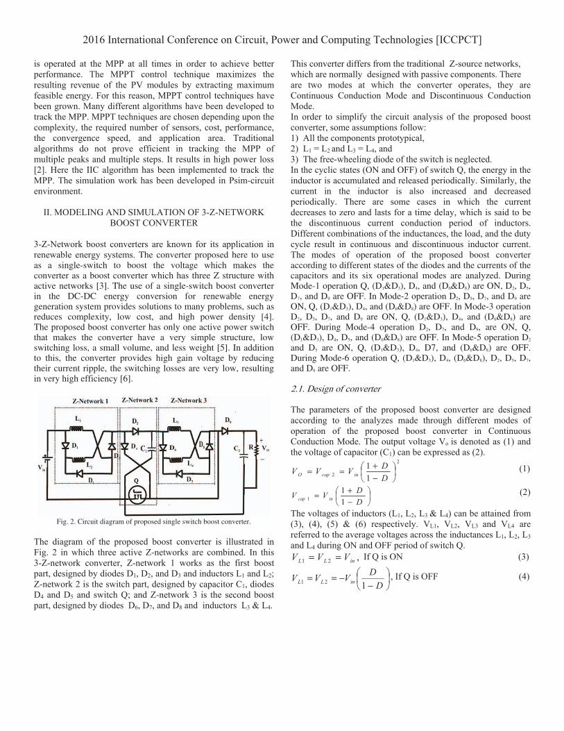
Fig. 2. Circuit diagram of proposed single switch boost converter.
The diagram of the proposed boost converter is illustrated in Fig. 2 in which three active Z-networks are combined. In this 3-Z-network converter, Z-network 1 works as the first boost part, designed by diodes D1, D2, and D3 and inductors L1 and L2; Z-network 2 is the switch part, designed by capacitor C1, diodes D4 and D5 and switch Q; and Z-network 3 is the second boost part, designed by diodes D6, D7, and D8 and inductors L3 & L4.
This converter differs from the traditional Z-source networks, which are normally designed with passive components. There are two modes at which the converter operates, they are Continuous Conduction Mode and Discontinuous Conduction Mode. In order to simplify the circuit analysis of the proposed boost converter, some assumptions follow: 1) All the components prototypical, 2) L1 = L2 and L3 = L4, and 3) The free-wheeling diode of the switch is neglected. In the cyclic states (ON and OFF) of switch Q, the energy in the inductor is accumulated and released periodically. Similarly, the current in the inductor is also increased and decreased periodically. There are some cases in which the current decreases to zero and lasts for a time delay, which is said to be the discontinuous current conduction period of inductors. Different combinations of the inductances, the load, and the duty cycle result in continuous and discontinuous inductor current. The modes of operation of the proposed boost converter according to different states of the diodes and the currents of the capacitors and its six operational modes are analyzed. During Mode-1 operation Q, (D1&D3), D4, and (D6&D8) are ON, D2, D5, D7, and D9 are OFF. In Mode-2 operation D2, D5, D7, and D9 are ON, Q, (D1&D3), D4, and (D6&D8) are OFF. In Mode-3 operation D2, D5, D7, and D9 are ON, Q, (D1&D3), D4, and (D6&D8) are OFF. During Mode-4 operation D2, D7, and D9, are ON, Q, (D1&D3), D4, D5, and (D6&D8) are OFF. In Mode-5 operation D2
and D5 are ON, Q, (D1&D3), D4, D7, and (D6&D8) are OFF. During Mode-6 operation Q, (D1&D3), D4, (D6&D8), D2, D5, D7, and D9 are OFF. 2.1. Design of converter The parameters of the proposed boost converter are designed according to the analyzes made through different modes of operation of the proposed boost converter in Continuous Conduction Mode. The output voltage Vo is denoted as (1) and the voltage of capacitor (C1) can be expressed as (2).
2
2 11
−+==
DD
VVV incapO (1)
−+=
DD
VV incap 11
1 (2)
The voltages of inductors (L1, L2, L3 & L4) can be attained from (3), (4), (5) & (6) respectively. VL1, VL2, VL3 and VL4 are referred to the average voltages across the inductances L1, L2, L3 and L4 during ON and OFF period of switch Q.
,21 inLL VVV == If Q is ON (3)
−−==
DD
VVV inLL 121, If Q is OFF (4)
2016 International Conference on Circuit, Power and Computing Technologies [ICCPCT]
−+−==
DD
VVV inLL 11
43 , If Q is ON (5)
−+−== 243 )1(
1DD
DVVV inLL, If Q is OFF (6)
As per the analysis of current in (7), it assumes that a lossless circuit leads to VinIin = VoIo, where Iin and Io are input and output currents, respectively. The currents of inductors (L1, L2, L3 & L4) can be attained from (8) & (9).
−+−= 2
2
)1()1(
DD
DII Oin (7)
−+−== 221 )1(
1DD
DIII OLL (8)
Similarly, IL3 and IL4 can be denoted as
−==
DD
III OLL 143 (9)
The parameter design of the inductor helps to estimate the value of rated current and inductance from the given preassigned variation range xL, an output voltage Vo, an output current Io, and a switching period T. The inductor ripple affects the stability of the converter. Therefore, the inductance must be designed in such a way that it can tolerate the ripples. The inductors in the proposed boost converter are designed based on (10), (11) & (12) respectively.
=Ldi
dtVL
LL (10)
when the switch Q is ON, the diL is the current ripple of the corresponding inductor within the time delay (dtL= DT) and the V L represents the voltage of the inductor. The permissible error of IL by diL is restrained by the preassigned variation range xL as diL = xLIL.. Hence, the range of the inductance is found by varying the duty cycle, and the maximum value obtained is taken as the rated value of inductance.
==L1L
in21 Ix
DTVLL (11)
+==
OL
in
IxDTDV
LL)1(
43 (12)
The parameter design of the capacitor estimates the rated voltage and capacitance from the given a preassigned variation range xcap, an output voltage Vo, an output current Io and a switching period T. The capacitor ripple affects the stability of the converter, whose permissible variation range can be used to
design the capacitance. Then, the value of capacitors in the proposed boost converter is designed from (13), (14) & (15) respectively.
=Cap
CapCap
dV
dtIC (13)
where ICap is the current of the corresponding capacitor when the switch Q is ON, the dtCap = DT is the time delay of the switch
as it is on, and dVCap is the ripple voltage corresponding to the capacitor within the time delay (dtCap). It denotes the permissible error of VCap by dVCap. dVCap is estimated by the tolerated variation range xCap as dVCap = xCapVCap when the switch Q is ON, ( ICap1 = 2IL3; ICap2 = Io ) .
=1
31
2
Capcap
L
VxDTI
C (14)
=ocap
o
VxDTI
C 2 (15)
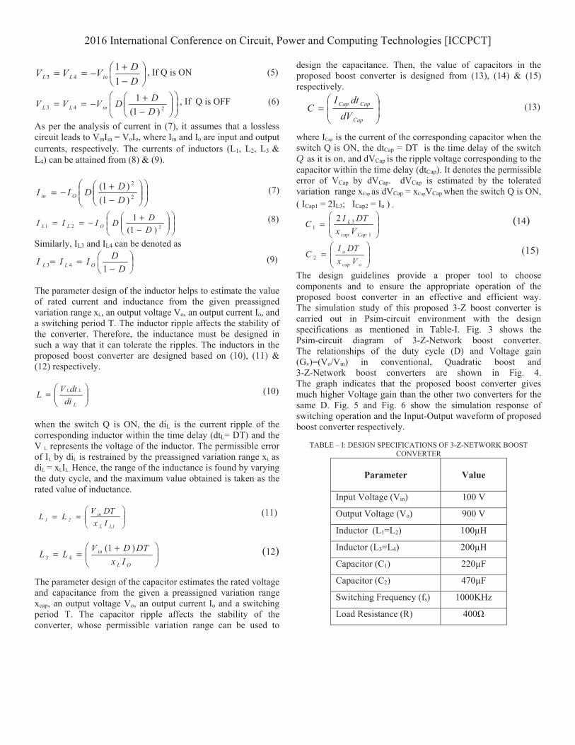
The design guidelines provide a proper tool to choose components and to ensure the appropriate operation of the proposed boost converter in an effective and efficient way. The simulation study of this proposed 3-Z boost converter is carried out in Psim-circuit environment with the design specifications as mentioned in Table-I. Fig. 3 shows the Psim-circuit diagram of 3-Z-Network boost converter. The relationships of the duty cycle (D) and Voltage gain (Gv)=(Vo/Vin) in conventional, Quadratic boost and 3-Z-Network boost converters are shown in Fig. 4. The graph indicates that the proposed boost converter gives much higher Voltage gain than the other two converters for the same D. Fig. 5 and Fig. 6 show the simulation response of switching operation and the Input-Output waveform of proposed boost converter respectively.
TABLE – I: DESIGN SPECIFICATIONS OF 3-Z-NETWORK BOOST CONVERTER
Parameter
Value
Input Voltage (Vin) 100 V
Output Voltage (Vo) 900 V
Inductor (L1=L2) 100μH
Inductor (L3=L4) 200μH
Capacitor (C1) 220μF
Capacitor (C2) 470μF
Switching Frequency (fs) 1000KHz
Load Resistance (R) 400
2016 International Conference on Circuit, Power and Computing Technologies [ICCPCT]
Fig. 3. Psim-circuit diagram of 3-Z Network boost converter.
Fig. 4. Voltage gain characteristics curve of boost converters for different values
of the duty cycle (D). Fig. 5. Simulation response of switching operation
Fig. 6. Simulation response of Input-Output waveforms of 3-Z Network boost converter.
2016 International Conference on Circuit, Power and Computing Technologies [ICCPCT]
III. MODELING AND SIMULATION OF PV ARRAY
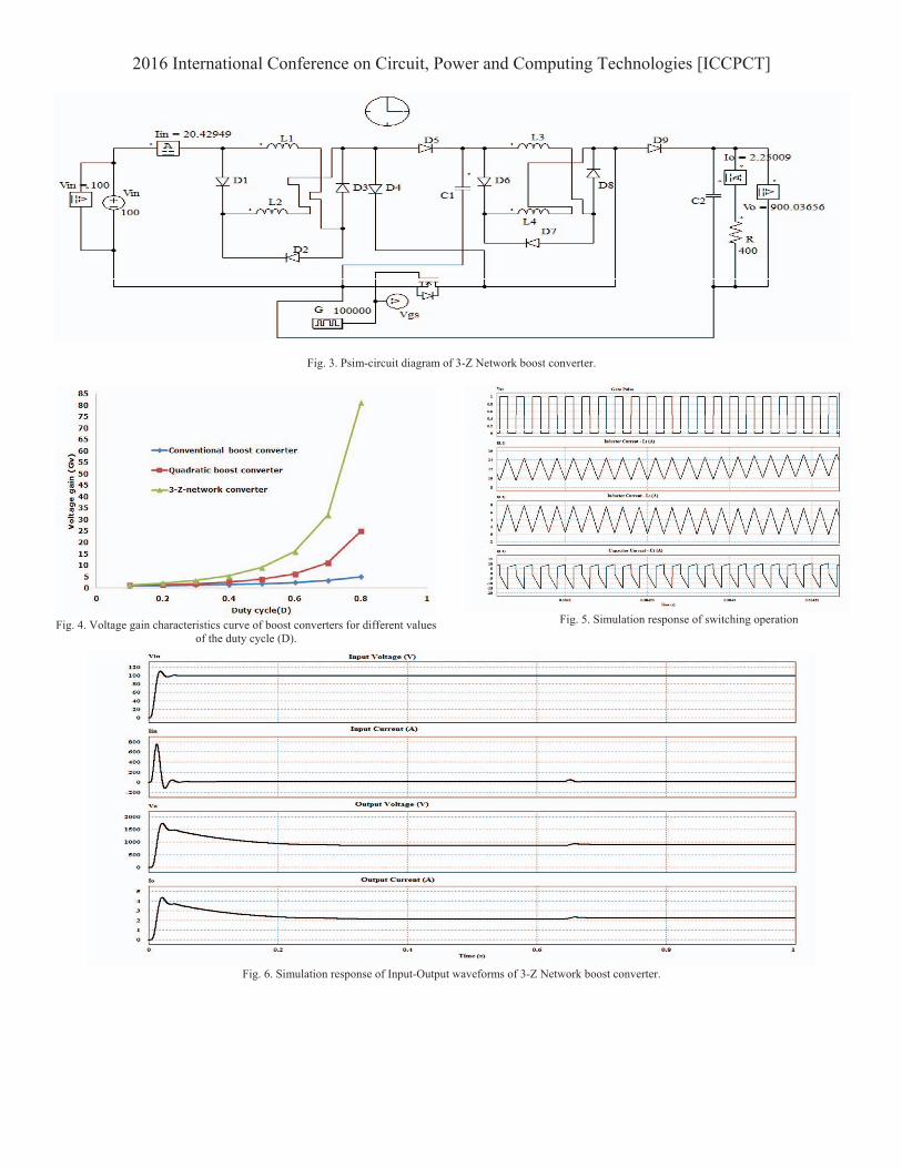
The PV array (3x3 PV modules) has been modeled and simulated in Psim-circuit environment as shown in Fig. 7. It is very significant to the placement of bypass diodes and blocking diodes in a PV array under partial shading conditions. The by-pass diode protects the PV module against Hot-Spot and damage of cells. The bypass diode helps to reduce the reverse voltage across the sub-module, therefore prohibiting the shading voltage drop within the string to the normal voltage of one sub-module (-0.7V). During night times when illuminated light does not fall on the modules are get illuminated light energy, an energy storage (like a battery, supercapacitors) connected directly in series with the modules connected the cells forward biased. This might enhance a discharge of the energy storage. A blocking diode is connected in series with the PV module prevents the discharge from energy storage device. But during normal illumination level, this diode leads to significant power loss [7, 8]. In modern PV modules has internally attached bypass diodes. Here, the PV array system has a different operating condition (Table-II) and their P-V and I-V characteristics have been observed. The simulated response indicates the multiple peaks and multiple steps in the modular characteristics of PV
array and it is plotted in Fig. 8 for the operating condition (pattern-II) respectively.
TABLE - II PV ARRAY UNDER DIFFERENT OPERATING CONDITION
PV array
Operating condition
Pattern-I Co25,2W/m1000Co25,2W/m1000Co25,2W/m1000
Co25,2W/m1000Co25,2W/m1000Co25,2W/m1000
Co25,21000W/mCo25,2W/m1000Co25,2W/m1000
Pattern-II Co30,2W/m600Co25,2W/m600Co25,2W/m800
Co25,2W/m400Co25,2W/m600Co30,2W/m600
Co30,2600W/mCo25,2W/m800Co25,2W/m800
Pattern-III Co30,2W/m400Co25,2W/m600Co25,2W/m800
Co25,2W/m600Co25,2W/m800Co30,2W/m400
Co30,2600W/mCo25,2W/m800Co25,2W/m1000
Fig. 7. Psim-circuit model of 3x3 PV array for Pattern-II.
2016 International Conference on Circuit, Power and Computing Technologies [ICCPCT]
Fig. 8. P-V and I-V characteristics of PV array for Pattern-II.
IV. MAXIMUM POWER POINT TRACKING
The commonly used MPPT is the Perturb and Observe (P&O) method which is also known as a hill-climbing algorithm. This technique uses a simple feedback arrangement and needs a calculation of only a few parameters. In this approach, the array voltage is changed periodically for the given perturbation and comparison of the previous output power to the present output power is done to calculate the MPP [9, 10]. On contrast, this method does not track the sudden change in irradiation levels. The MPPT method that is described here is Incremental Conductance (IC) method. It helps to find and adjust the array operating voltage to maintain MPP condition through simple incremental conductance and instantaneous conductance measurements [11, 12]. P&O and IC MPPT controllers have been employed along this proposed boost converter for comparing their performance analysis and efficiency. The Improved Incremental Conductance (IIC) MPPT algorithm is also illustrated in this research work where it initiated on the value of the derivative of the panel current over the panel voltage. Comparison of instantaneous conductance to the incremental conductance tracks the MPP. Based on it the reference voltage (Vref) from the PV is increased or decreased with a small change in values to make the PV array operate at MPP. The knowledge of Vref makes the IIC implementation easier. Considerably, the tracking time of the algorithm is also reduced. The Fig. 9 shows the flowchart of IIC MPPT algorithm to locate MPP at different operating conditions. The MPP reference voltage is expressed as the product of the open circuit voltage and constant ( ). It is denoted in the following linear equation (16).
ocref VV α= (16)
The value of varies from 0.73 to 0.80 depending upon the PV cell characteristics.
Fig. 9. Flowchart of IIC MPPT algorithm.
These are the important features of IIC,
Real-time implementation becomes easy as computation burden is reduced.
It tracks the MPP efficient at multiple peaks and multiple steps.
Earlier knowledge reduces the tracking time of the algorithm.
Maximum power loss is less in the proposed MPPT algorithm.
The effectiveness of the IIC algorithm is more compatible and stable than the other two algorithms.
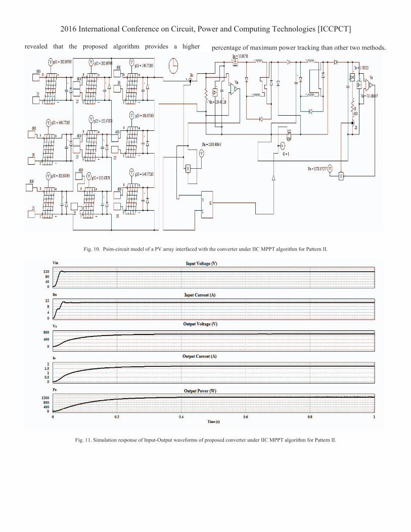
Fig. 10 shows Psim-circuit model of a PV array interfaced with the proposed boost converter using IIC MPPT algorithm for Pattern II. The duty cycle under the different operating condition is fed to the proposed boost converter for proper switching operation of the system at MPP. From the simulation results, it is
2016 International Conference on Circuit, Power and Computing Technologies [ICCPCT]
revealed that the proposed algorithm provides a higher percentage of maximum power tracking than other two methods.
Fig. 10. Psim-circuit model of a PV array interfaced with the converter under IIC MPPT algorithm for Pattern II.
Fig. 11. Simulation response of Input-Output waveforms of proposed converter under IIC MPPT algorithm for Pattern II.
2016 International Conference on Circuit, Power and Computing Technologies [ICCPCT]
The simulation responses have been illustrated in Fig. 11. Under PSC, PV modules belonging to the same string undergo different insolation and temperature. The resulting P–V characteristic curve becomes more complex and reveals multiple peaks. The presence of multiple peaks decreases the effectiveness of the system. Moreover, P&O and IC are not tracking the MPP effectively than IIC MPPT algorithm under these conditions. Table-III shows the comparisons of the MPPT algorithms. The IIC tracks more power than other two algorithms.
TABLE – III: COMPARISONS OF THE MPPT ALGORITHMS
Pattern
MPPT
(Pin) W
(Iin) A
(Po) W
(Io) A
( ) %
I
P&O 2269.1 20.22 2243 2.37 98.85
IC 2269.1 20.22 2244 2.37 98.89
IIC 2268.9 20.22 2247 2.37 99.04
II
P&O 1291.8 10.81 1264 1.79 97.84
IC 1291.7 10.81 1273 1.79 98.55
IIC 1291.6 10.81 1279 1.79 99.02
III
P&O 1133.7 15.05 1115 1.67 98.35
IC 1133.7 15.05 1116 1.67 98.44
IIC 1133.6 15.05 1119 1.67 98.70
V. CONCLUSION
The performance of 3-Z-Network boost converter for a standalone Photovoltaic (PV) power generation system under different shading patterns of solar irradiation has been investigated in this proposed work. The Voltage gain (Gv) characteristic curve of this converter circuit has been studied for various duty cycle (D) and it is compared with conventional & Quadratic boost converters. But, the 3-Z-Network boost converter provides good voltage gain ratio. The developed converter model and the Input-Output response have been analyzed under different operating modes. Further, this proposed converter is integrated with the Photovoltaic panel for the harvesting of solar energy. The modular characteristics of PV module under different irradiance level and temperature have been analyzed using Psim-circuit environment. During the PSC, multiple peaks and multiple steps are noticed in the P-V & I-V characteristics curves respectively. Here, the P&O, IC and IIC algorithms have been incorporated for finding the MPP under different operating conditions. The effectiveness of the IIC technique adopted in this work for finding MPP has been evaluated and the simulation results are compared with P&O and
IC methods. The simulation results show that the IIC algorithm overcomes the drawbacks of conventional algorithms where it fails to track the MPP effectively under PSC. Moreover, the 3-Z structure of the converter improves the energy conversion efficiency of an integrated Photovoltaic system for promoting the green energy. In addition, this converter-PV system can be connected with suitable storage systems for meeting the power demand during night time and low irradiation conditions.
REFERENCES
[1] J. Parikh and K. Parikh, “Growing pains: Meeting India’s energy needs in the face of limited fossil fuels,” IEEE Power Energy Mag., vol. 10, no. 3, pp. 59–66, May 2012.
[2] F. Ansari, A. K. Jha, “Maximum power point tracking using perturbation and observation as well as incremental conductance algorithm,” International journal of research in engineering & applied sciences, issn: 2294-3905, pp. 19-30, 2011.
[3] Y. Tang, T.Wang, and Y. He, “A switched-capacitor-based active-network converter with high voltage gain,” IEEE Trans. Power Electron., vol. 29, no. 6, pp. 2959–2968, Jun. 2014.
[4] D. S. Wijeratne and G. Moschopoulos, “Quadratic power conversion for power electronics: Principles and circuits,” IEEE Trans. Circuits Syst. I, Reg. Papers, vol. 59, no. 2, pp. 1967–1979, Feb. 2011.
[5] K. I. Hwu, C. F. Chuang, and W. C. Tu, “High voltage-boosting converters based on bootstrap capacitors and boost inductors,” IEEE Trans. Ind. Electron., vol. 60, no. 6, pp. 2178–2193, Jun. 2013.
[6] C.-M. Young, M.-H. Chen, T.-A. Chang, C.-C. Ko, and K.-K. Jen, “Cascade Cockcroft–Walton voltage multiplier applied to transformerless high step-up DC–CDC converter,” IEEE Trans. Ind. Electron., vol. 60, no. 2, pp. 523–537, Feb. 2013.
[7] R. Pon Vengatesh, S. Edward Rajan, “Investigation of the effects of homogeneous and heterogeneous solar irradiations on multi-crystal PV module under various configurations,” IET Renewable Power Generation, vol.9, no. 3, pp. 245-254, Apr. 2015.
[8] Y. Mahmoud, W. Xiao, and H. H. Zeineldin, “A simple approach to modeling and simulation of photovoltaic modules,” IEEE Trans. Sustain. Energy, vol. 3, no. 1, pp. 185–186, Jan. 2012.
[9] M. de Brito, L. Galotto, L. Sampaio, G. de Azevedo e Melo, and C. Canesin, “Evaluation of the main mppt techniques for photovoltaic applications,” Industrial Electronics, IEEE Transactions on, vol. 60, no. 3, pp. 1156–1167, 2013.
[10] H. Al-Atrash, I. Batarseh, and K. Rustom, “Effect of measurement noise and bias on hill-climbing MPPT algorithms,” IEEE Trans. Aerosp. Electron.Syst., vol. 46, no. 2, pp. 745–760, Apr. 2010.
[11] Reza Reisc Ali, Hassan Moradi Mohammad, Jamasb Shahriar. “Classification and comparison of MPPT techniques for PV system: a review,” Renew Sustain Energy Rev 2013; 19:433-43.
[12] Ji Young-Hyok, Jung Doo-Yong, Kim Jun-Gu, Kim Jae-Hyung, Lee Tae-Won. Won Chung-Yuen, “A real maximum power point tracking method for mismatching compensation in PV array under partially shaded conditions,” IEEE Trans Power Electron, Apr. 2011; 2 6 (4).