INFORMATION TO USERS This manuscript has been repmduced from the microfilm master- UMI films the text directly from the original or copy submitteded Thus, some thesis and dissertation copies are in typewfiter face, wtiile others may be from any type of cornputer pnnter. The quality of this reproduction is dependent upon the quality of the copy submitted. Broken or indistinct print, colored or p w r quality illustrations and photographs, print bieedthrough, substandard margins, and impmper alignment can adversel y affect reproduction. ln the unlikely event that the author did not send UMI a camplete manuscript and there are missing pages, these will be noted. Also, if unauthorized copyright matenal had to be removed, a note will indicate the deletion. Ovenize materials (e-g., maps, dMngs, charts) are reproduced by secüoning the original, beginning at the upper left-hand corner and continuing from left to tight in equal sections with small overfaps. Photographs included in the original manuscript have been reproduced xerographically in this copy. Higher quality 6" x 9" black and white photographic prints are available for any photographs or illustrations appearing in this copy for an additional charge. Contact UMI direcüy to order. Bell & Howell Informationand Leaming 300 North Zeeb Road, Ann Ahor, MI 48106-1346 USA
Transcript
INFORMATION TO USERS
This manuscript has been repmduced from the microfilm master- UMI films the
text directly from the original or copy submitteded Thus, some thesis and
dissertation copies are in typewfiter face, wtiile others may be from any type of
cornputer pnnter.
The quality of this reproduction is dependent upon the quality of the copy
submitted. Broken or indistinct print, colored or p w r quality illustrations and
photographs, print bieedthrough, substandard margins, and impmper alignment
can adversel y affect reproduction.
ln the unlikely event that the author did not send UMI a camplete manuscript and
there are missing pages, these will be noted. Also, if unauthorized copyright
matenal had to be removed, a note will indicate the deletion.
Ovenize materials (e-g., maps, dMngs, charts) are reproduced by secüoning
the original, beginning at the upper left-hand corner and continuing from left to
tight in equal sections with small overfaps.
Photographs included in the original manuscript have been reproduced
xerographically in this copy. Higher quality 6" x 9" black and white photographic
prints are available for any photographs or illustrations appearing in this copy for
an additional charge. Contact UMI direcüy to order.
Bell & Howell Information and Leaming 300 North Zeeb Road, Ann Ahor, MI 48106-1346 USA
Investigation of High Power DFB Lasers: Operating Mechanisms, Electro-Opto-Thermal Interactions
Keith Lee
A thesis submitted in conformity with the requirements for the degree of Doctor of Philosophy
Graduate Department of Electrical and Computer Engineering Universis- of Toronto
@Copyright by Keith Lee (1 998)
National Library I*I of Canada Bibliothèque nationale du Canada
Acquisitions and Acquisitions et Bibliographic Services services bibliographiques
395 Wellington Street 395. rue Wellington Ottawa ON K1A ON4 Ottawa ON K1A O N 4 Canada Canada
Your Ifle Votre rciferenœ
Our fi& Noire reférence
The author has granted a non- exclusive licence allowing the National Library of Canada to reproduce, loan, distribute or sell copies of this thesis in microfom, paper or electronic formats.
The author retains ownership of the copyright in this thesis. Neither the thesis nor substantial extracts £kom it may be printed or otherwise reproduced without the author7 s permission.
L'auteur a accordé une licence non exclusive permettant à la Bibliotheque nationale du Canada de reproduire, prêter, distribuer ou vendre des copies de cette thèse sous la forme de microfiche/nlm, de reproduction sur papier ou sur format électronique.
L'auteur conserve la propriété du droit d'auteur qui protège cette thèse. Ni la thèse ni des extraits substantiels de celle-ci ne doivent être imprimés ou autrement reproduits sans son autorisation.
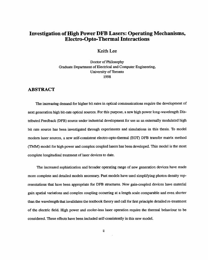
Investigation of High Power DFB Lasers: Operating Mechanisms, Electro-Opto-Thermal Interactions
Keith Lee
Doctor of Philosophy Graduate Department of Electricai and Cornputer Engineering,
University of Toronto 1998
ABSTRACT
The increasing demand for higher bit rates in optical communications require the development of
next generation high bit-rate optical sources. For this purpose, a new high power long-wavelength Dis-
tributed Feedback (Dm) source under industrial development for use as an externally modulated high
bit rate source has been investigated through experiments and simulations in this thesis. To model
modern laser sources, a new self-consistent electro-op to-thermal (EOT) DFE3 tram fer matrix method
(T'MM) model for hi@ power and complex coupled lasers has been developed. This mode1 is the most
complete longitudinal treatment of laser devices to date.
The uicreased sophistication and broader operating range of new generation devices have made
more complete and detailed models necessary. Past models have used simpli@ing photon demity rep-
resentations that have been appropriate for DFB structutes. New gain-coupled devices have material
gain spatial variations and complex couphg occxmhg at a length scaie comparable and even shorter
than the wavelength that invalidates the textbook theory and caii for tirst principle detailed re-treatment
of the electric field. High power and cooler-less laser operation require the thermal behaviour to be
considered. These effects have been included self-consistently in this new model.
Application of the EOT mode1 to two illustralive modem devices are presented. W1th the model,
the performance of a new Roating Grating (FG) DFE3 structure was characterized, in this example, the
analysis has included 2-D and 3-D effects with finite element andysis. The device Iacks of prior analy-
sis because of its complexity and its unusually high injection Ievel. Detailed experimental measure-
ments including L-1, active region temperature with increasing bias, below and above threshold spectra
and the SMSR were made to compare with the model results and show that the unoptimized FG device
has retained a comparable performance to standard DFB devices while eliminating a critical process
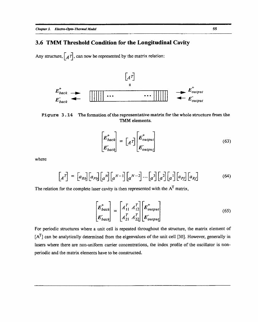
dependent uncertainty. A limitation to the FG DFB approach was greater active region heahg. Using
the EOT DFB TMM model and anaIysis from the finite element light emitting simulator (FELES) the
carrier transport through the FG structure was examined. The analysis offers the first detail 2D longitu-
dinal examination of FG structure, The model predictions were compared to the measured data for the
high power FG DFB laser and showed good agreement. The model was then applied to irnprove the
high power design. Further analysis show that by chanping the FG composition alone, the output
power from the FG design couid be increased by 20%. As a second example, the model has been used
to examine the threshold current and L-1 hearity for in-phase and out-of-phase gain coupled devices
by explicitly including electric field coherence r d t i n g in the standing wave effect.
The self-consistent electro-opto-thermal model developed in this thesis serves as both a usefbl
design tool and a means for fundamental investigations into device physics providing deeper under-
standing of the complicated DFB device operation in the new higher power regime. Whrle this work
has focused on two particular types of laser devices, the electro-opto-thermal TMM model is readily
appLicable to 1-D analysis of any arbitrary structure.
..- Ill
Acknowledgments
1 would like the express my gratitude to many people without whom 1 would not have been able to
complete this work: Fiist, 1 wouId like to th& Mabel, my family and fnends for their belief in me and
their loving support; 1 would like to thank rny supervisor Prof. J.M. Xu for his guidance and support
during the course of this work; Mr. G.L. Tan, who developed the F.E.L.E.S. model, and who has
always encouraged me in my research; The past and present members of the Optoelectronics Lab for
their help and friendship; Our industnal research coUaborators at the Norte1 Advanced Technology
Laboratory, Dr. T. Makino and Dr. G. Pakulski, who supplied the laser devices that were studied in this
thesis and who have generously extended to us the use of their lab at the Carling Research Facility in
Nepean; and Ms. Sarah Cherian for her encouragement in cornpleting this work.
I would aIso like to th& Dr. Hanh Lu of Lasertron, for his critical review of the work and my
cornmittee members Prof. S. Zukotynski, Prof. W.T. Ng, Prof. J.R. Long and Prof. M.R. Iravani for
their heipful comments.
Table of Contents
CHAPTER 1 Electro-Opto-Thermal T r d e r Matrix Model for High ......... Power Distributed Feedback Lasers .................. .......... 13
1.1 Introduction ..................................................................................................................... 13 ..................................................................................................... 1.2 Organkation of Thesis 15
C W T E R 2 The Development of Lasers for Optical Communications .. 17
2.1 Optical Source for High Bit Rare Digital Systems ..................................................... 17
.............................................. 2.2 Long-wavelength Lasers for Fiber Op tic Communication 18 2.2.1 FiberLoss .......................................................................................................... 18 22.2 Fiber Dispersion ................................................................................................ 19
.......................................................................................... 2.3.3 Gain Coupled b e r 25 2.4 Longitudinal Laser Mode1 Development ......................................................................... 27
3.3 Maxwell's Equations ..................................................................................................... . 36 3.3.1 Plane Wave Representation and the Complex Propagation Constant ................ 39
.................................................................................................. 3.4 Transfer Matrix Method 41 ............................................................................................ 3.4.1 TE TIblM Relations 42
3.4.2 Matrices for one period ............................ .. .................................................... 42 3.4.3 TM TMM formulation ....................................................................................... 47
3.6 l'MM Threshold Condition for the Longitudinat Cavity ...........................es........ ... . . . 55
3.7 ElecCric Field vs . Average Photon Density ...................................................................... 58 ...................................................................... 3.7.1 M o a e d Photon Rate Equation 59
..................................................................................................... 3.7.2 Output Power 61 ............................................................................................... 3 -8 The Canier Rate Equation 62
........................................................................................ 3.8.3 Auger Recombination 64 ..................................................... 3.8.4 StimuIated Recombmation and Modal Gain 64
3.8.5 Lateral Spread and Thennionic Ieakage cment ............................................ 65 3.9 Material Refractive Index and Carier Concentration .............................................. 65
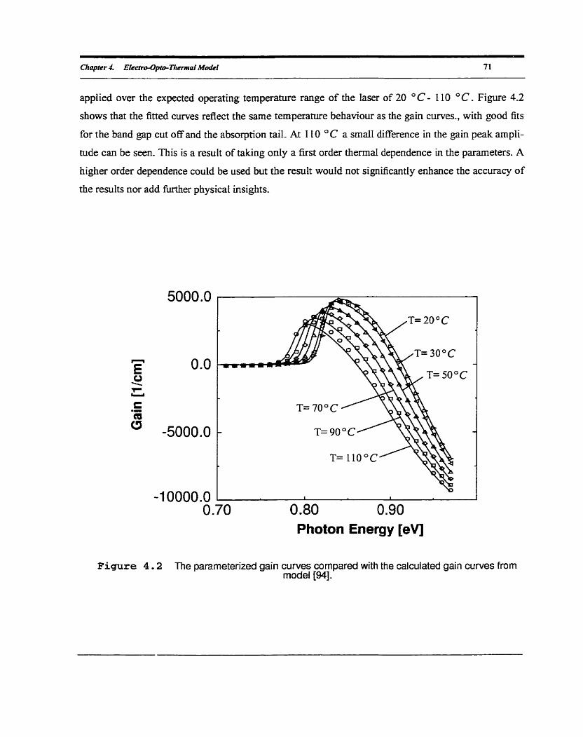
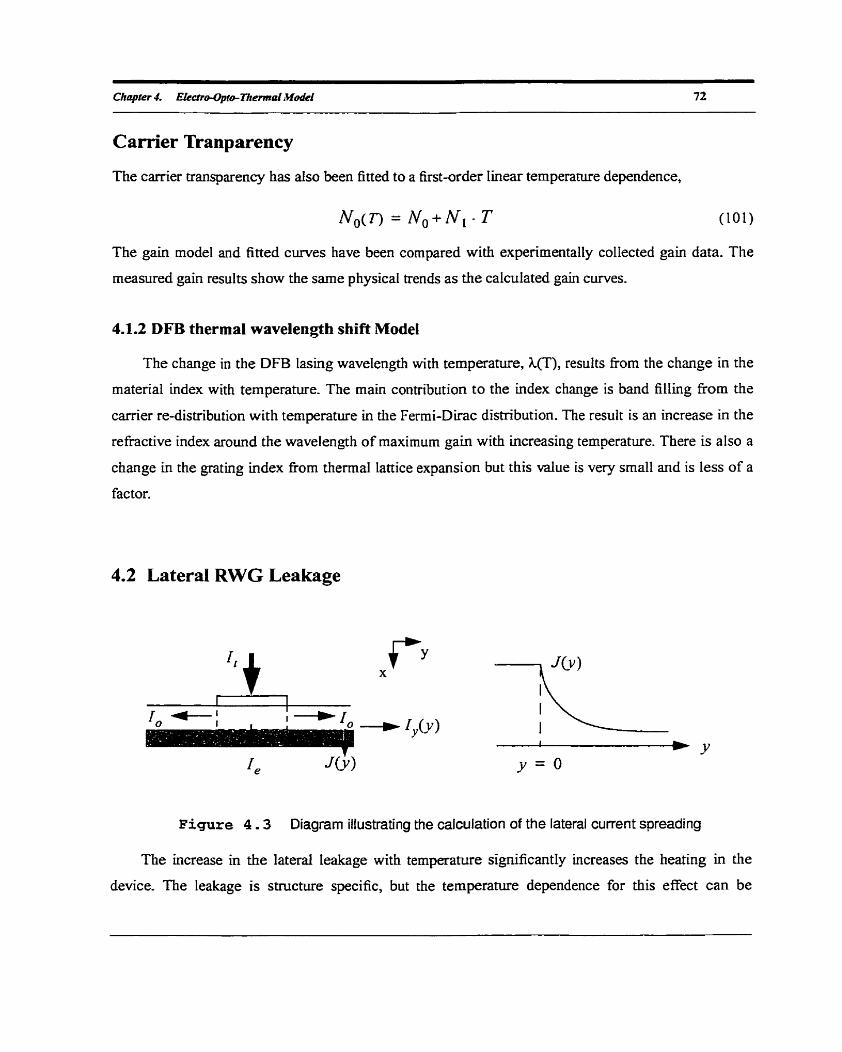
CHAPTER 4 Electro-Opto-Thermal Model ............................................... 68
Part II: Thermal Mode1 for High Power 1.55 p laser ................................. 68 ............................................................................................................ 4.1 Thermal De tuning 69
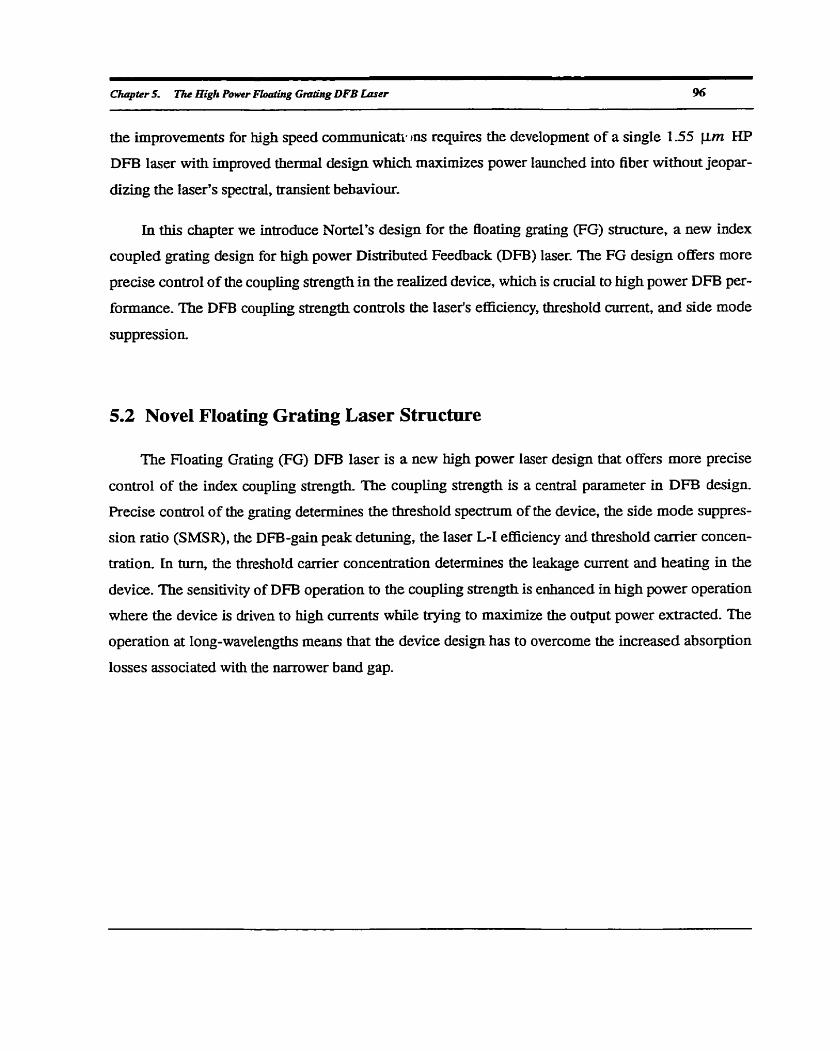
CHAPTER 5 The High Power Floating Grating DFB Laser ..................... 95
5.1 High Power DFB Laser for High Bit Rate Source ................................................... 95
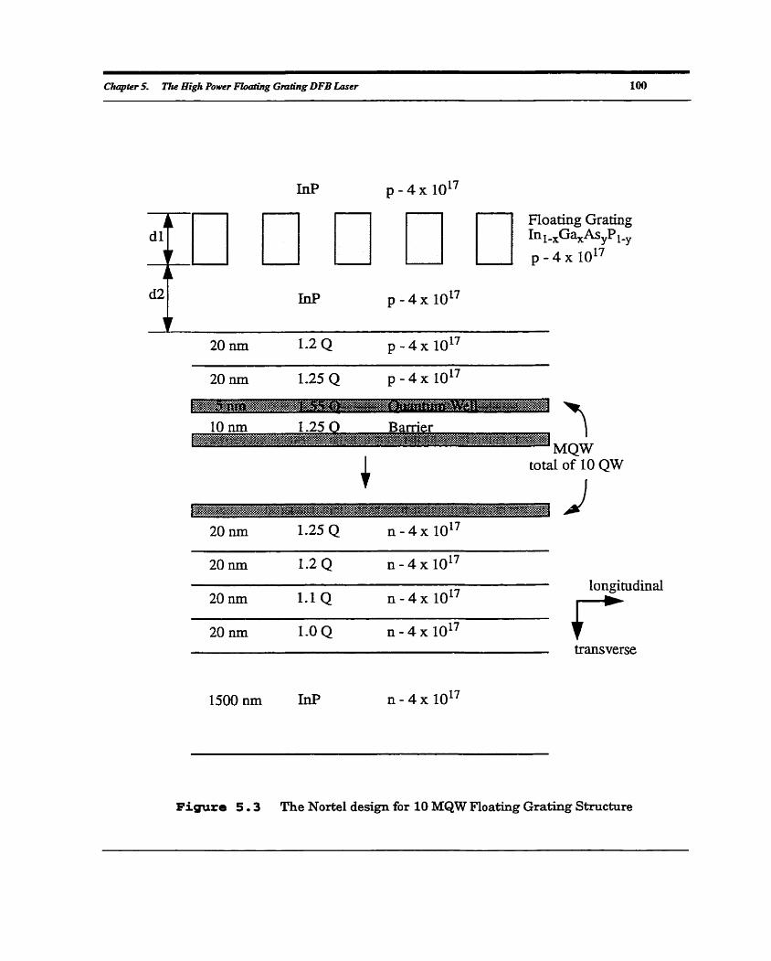
5.2 Novel Floating Grating Laser Structure .......................................................................... 96 .............................................................................. 5.2.1 Control of coupling strength 98
..................................................................................... 5.2.2 The Grating Structure 101 ................................................................................................... 5.2.3 M a & L-1 101
......................................... 5.3 High Power Design Considerations .......................... ...... 103
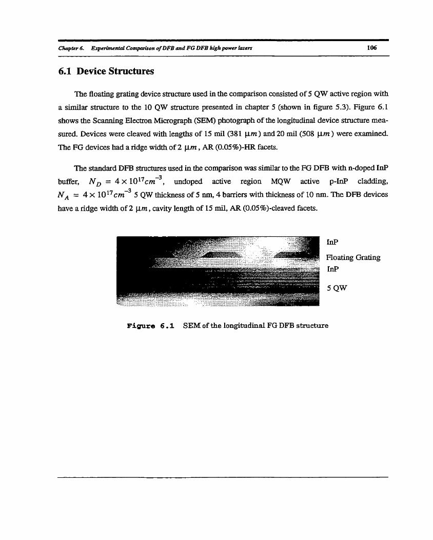
CHAPTER 6 Experimentai Comparison of DFB and FG DFB high power .................................................................................... lasers 105
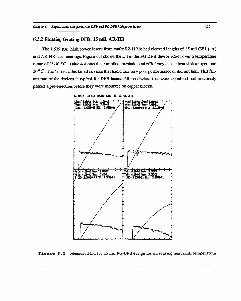
............................................ 6.3 Cornparison of FG DFB and conventional DFB structure 109 .................................................................................................... 6.3.1 DFB devices 109
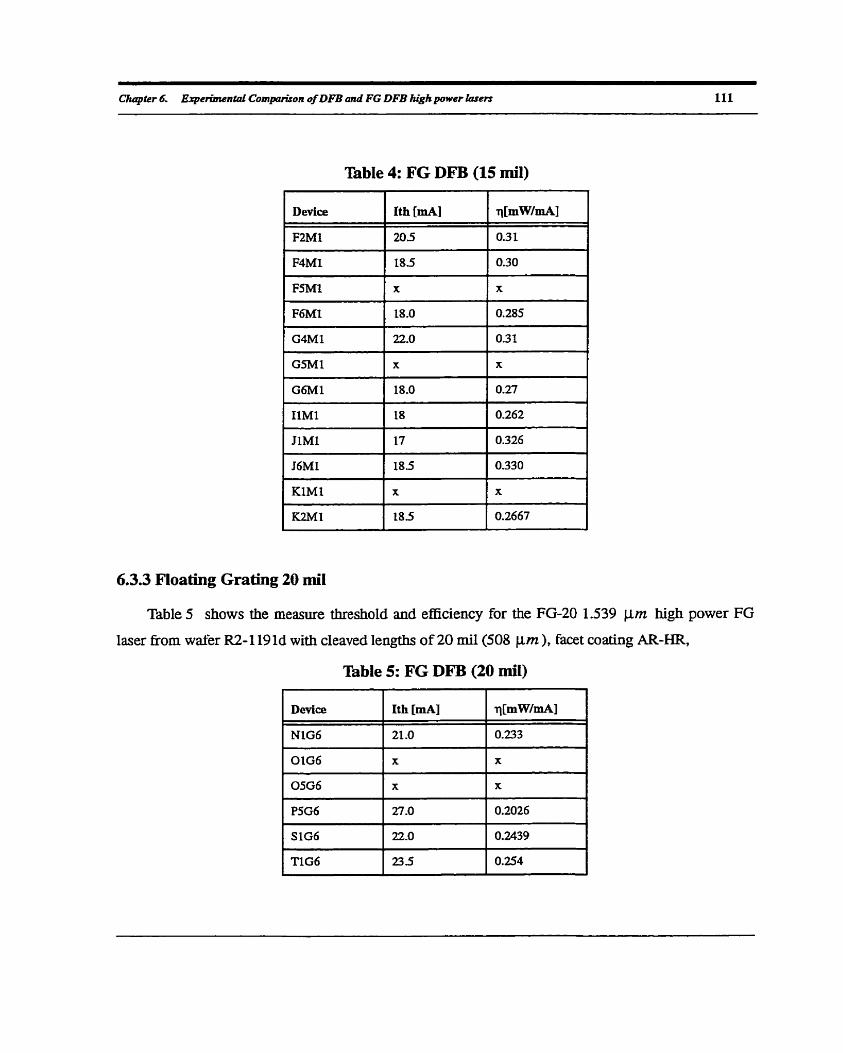
................... .................................. 6.3.2 FIoating k t i n g DFB, 15 mil, AR-HR ,., 110 ................................................................................... 6.3 -3 F'ioating Grating 20 mil 111
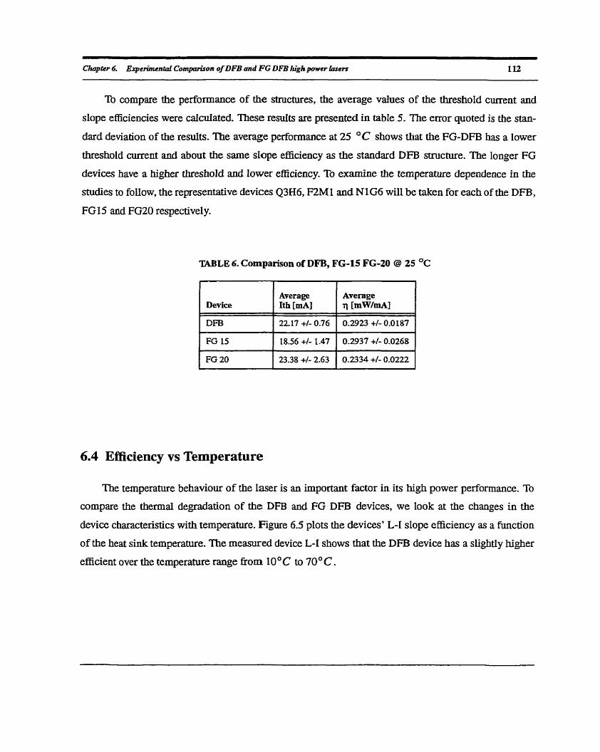
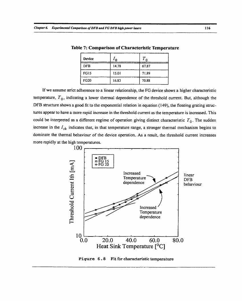
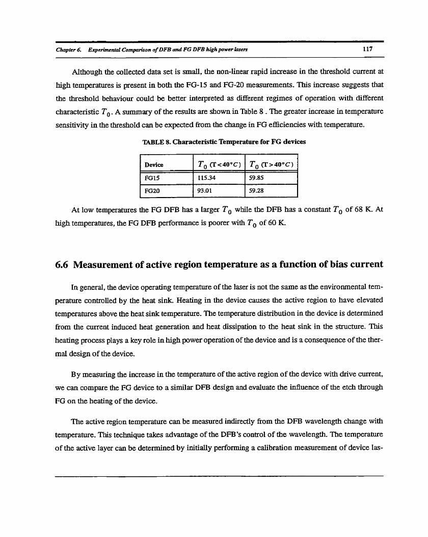
6.5 Temperature dependeace of the threshold current ........................................................ 114
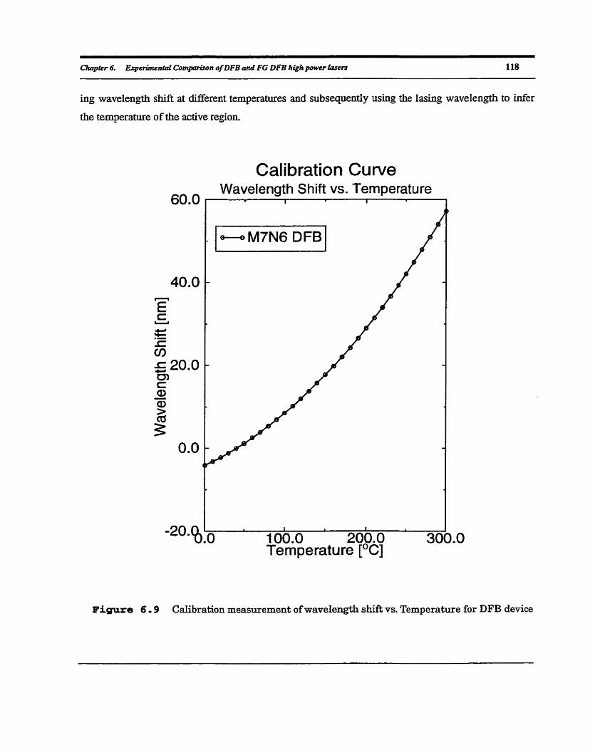
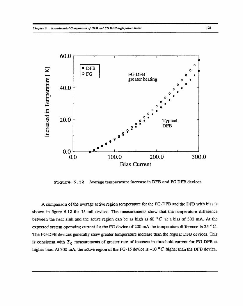
...................... 6.6 Measurement of active region temperature as a function of bias cunent 117
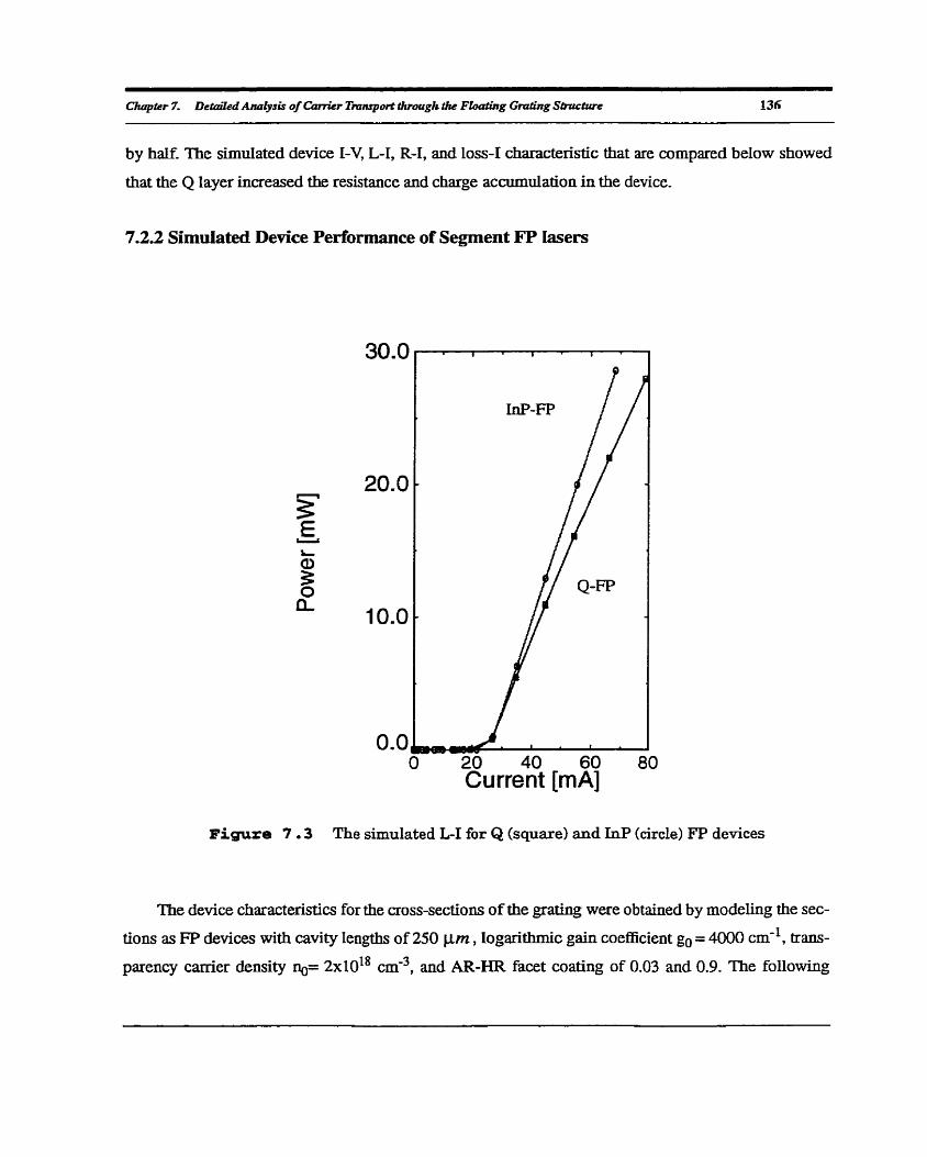
CHAPTER 7 Detailed Anaiysis of Carrier Transport through the Floating Grating Structure .... .. ............................................................ 132
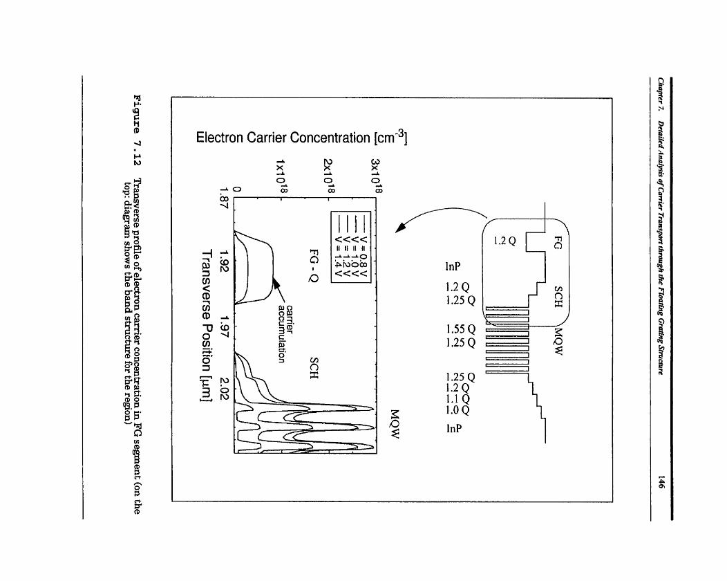
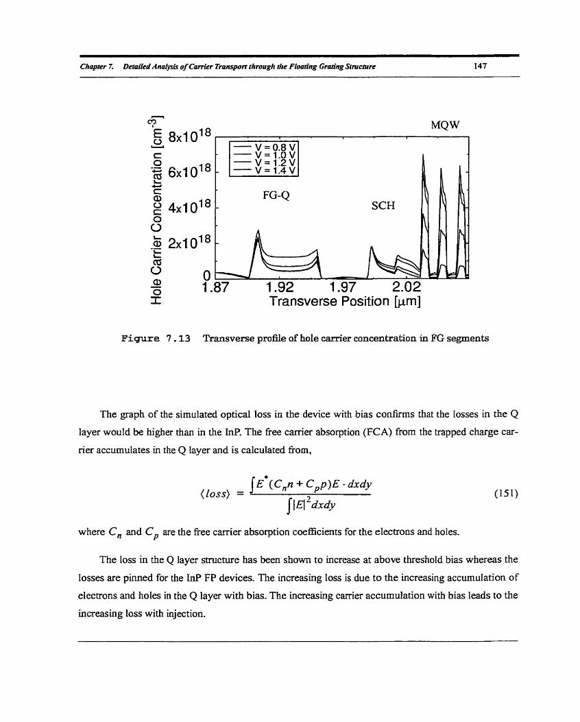
.......................................................................................... 7.2.5 Carrier Distribution 145 7.2.6 Summary .......................................................................................................... 148
........................................................................... 7.3 Part II: Longitudinal Carrier Analysis 150 ............................................................ 7.3.1 Longitudinal Canier Transport Mode1 150
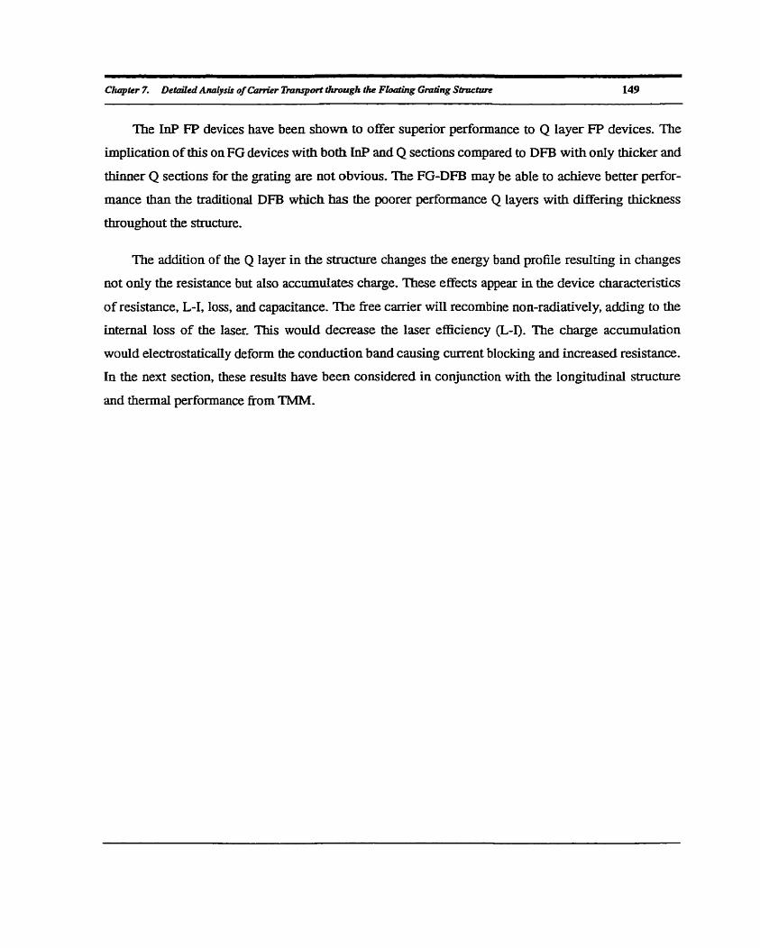
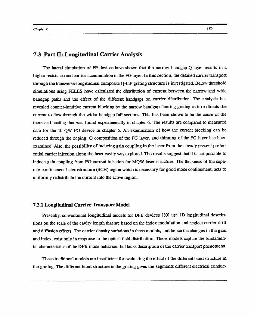
............................... 7.3.2 FELES Below Threshold Longitudinâl Electricai Mode1 151 ................................................................................ 7.3.3 Longitudinal m e n t flow 153
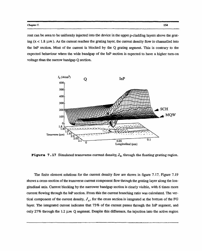
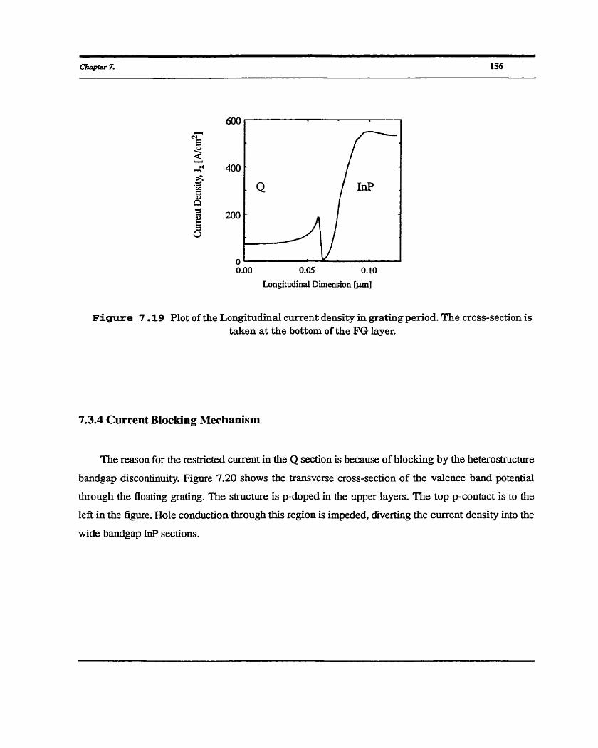
.......................................................................... 7.3.4 Current Blocking Mechankm 156 ....................................... 7.3.5 Longitudinal carrier accumulation in the Q sections 158
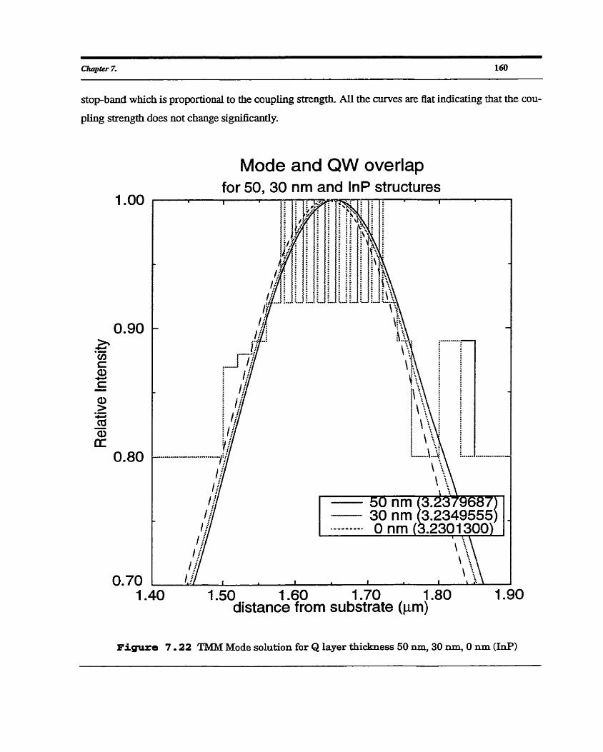
...................................................... 7.4 Cornparison of 10 MQW Device to Mode1 Resuits 159 .................................................................................................... 7.5 Design Irnpmvements 163
........................................................ 7.6 Possibility of Improvements fkom Gain Coupling 169
CHAPTER 8 Application of TMM model: The Interference Effect in Gain Coupled devices ..................................................................... 174
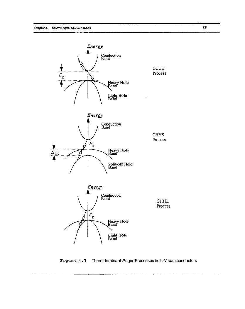
coefficient for non-radiative recombination fiom defect States
coefficient for bimolecular recornbination rate
magnetic flux density speed of light in vacuum loss coefficient for electrons and holes
active layer thickness thickness of the thermal Iayer
electnc flm density carrier diffusion coefficient minonty electron dinusion coefficient
change in the auger recombination rate with temperature
electric field vector
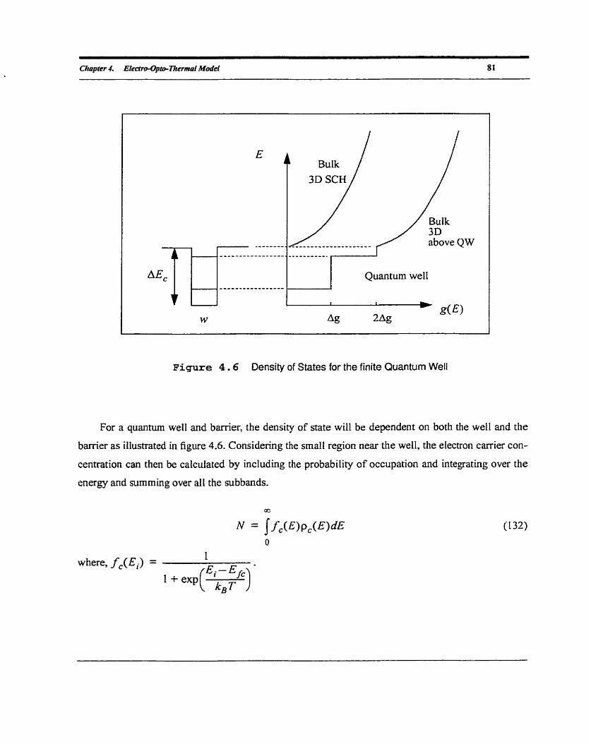
complex vector amplitude of electtic field scalar wave amplitude
electric field amplitude of forward travelling plane wave
electric field amplitude of backward travelling plane wave total elzctric field amplitude fermi level
quantum weIl energy levels
Auger threshold energy
fermi function
relative photon distribution
material gain gain coefficient
step height of stak density in quantum well net gain modal gain
d IP 4 h
i
3 j
ko
k~ K L
LC,,
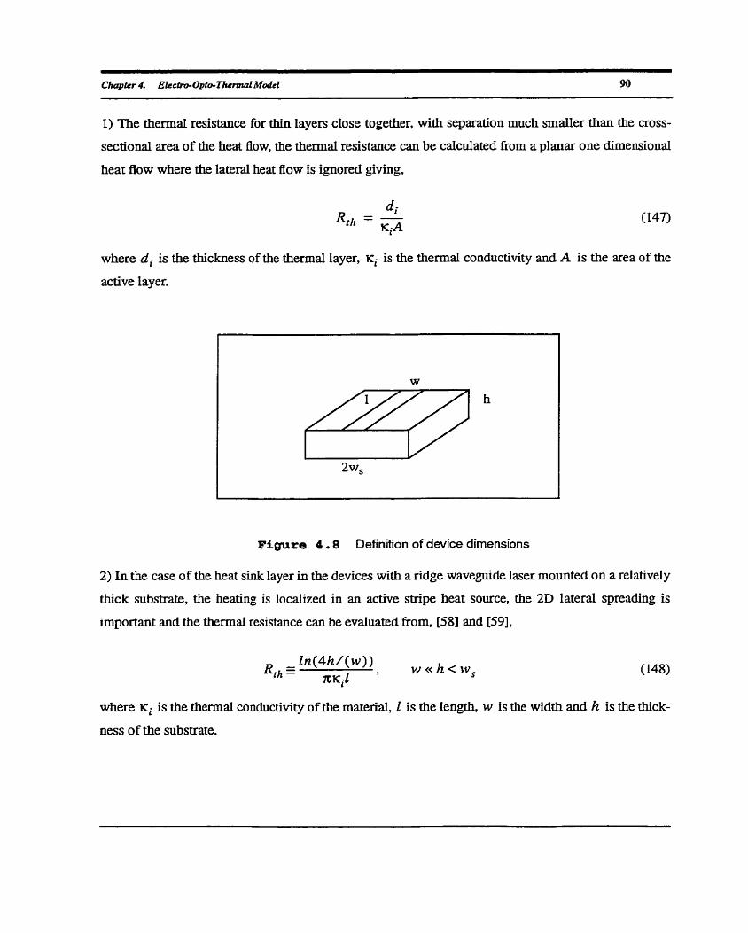
L n
ms
m~~~
mco * w
R
n
II r
ng i
bias ni
O n i
ND
N A N
Nb
NCC
Pdissipoted
magnetic field vector
cornplex vector amplitude of magnetic field vector threshold cwrent
current
current density vector imaginary unit vacilum wave nurnber
Boltzmann's constant
surface current light Intensity cavity length
minority electron diffusion length
split-off band effective mass
heavy hole effective mass
conduction band effective mass
quantum well effective mass
effective mass of the cladding section
non-ideality constant complex modal index red p u t of the refractive index of the waveguide
group index
complex index with injection
passive complex index without injection
donor doping
acceptor doping
carrier density concentration of the minorisr electrons at the edge of the P-cladding Iayer
density of States coefficients detemined from the
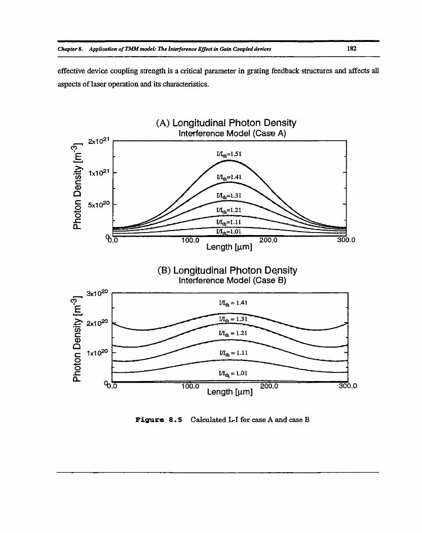
power dissipated
polarization of medium
complex vector amplitude of polarization of medium
photon density in the k~ section
photon density normalization factor
output power from front facet
photon density
electron charge refiection coefficient re flectance radiative and non-radiative recombination processes. non-radiative recombination rates from defects
auger recombination rate
spontaneous recombination rate
stirnulated recombination rate
resis tance thermal resis tance
average Po ynting vector or the irradiance abs olute temperature transmittance characteris tic temperature
group velocity
depth of the weLl in the conduction band
voltage P-cladding layer thickness
characteristic length of the drift leakage
attenuation constant or the net power absorption coefficient intemd loss
threshold gain
complex propagation optical confinement factor
split-off energy complex dielectric constant real part of dielectric constant
imaginary part of dielectric constant
permittivity of vacuum
slope efficiency
thermal conductivity
grating coupling coefficient vacuum permeability
electron mobility
charge density density of States
electron wave function conductivity of medium transmission coefficient minority carrier life t h e
medium suscep tibility medium suscep tibility without extemal pumping
change in the susceptibiIity due to concentration of charge carriers
angular frequency
ChpCrr 1. ElecbPOpto-ThemL Transfer MarN: Model for Eigh Power Dkbauled Feedback Lasm 13
Chapter 1
Electro-Opto-Thermal ïkansfer Matrix Model for High Power Distributed Feedback Lasers
1.1 Introduction
The advantages of high information capacity and low transmission Iosses have made fiber optical
systems the dominant carrier systems used in present day long-haul communications. Current com-
mercial digital systems, such as the OC-48, with bit rates of 2.4 Gigabits per second (Gb/s), have been
obtained using single fiequency, index coupled distributed feedback (Dm) semiconductor lasers as
the optical transmission sources. Future projections for broadcast transmission, internet, voice and
multimedia services indicate that greater capacity and higher modulation rates will be needed. Such
demands cannot be met by incremental improvements to conventional DFB laser designs. Above 2.4
Gb/s, the modulation rates of directly rnodulated DFB Iasers become limited by wavelength chirp [Il.
Hence new optical sources and laser structures such as hybrid aod integrated externaliy modulated
sources need to be developed The use of these extemally moddated sources in a high bit rate system
inîroduces an additional insertion Ioss to the system. In order to obtain the required powers and retain
the benefits fiom the spectral properties of the DFB source, it becomes necessary to develop high
power DFB lasers.
Chaptér I . E L e c t m - O p - T h c d Tm&r Mu& Mdel for Eigh Power Disaioutcd Feedback Lasecs 14
Today's laser structures have reached a very high level of complexity. To improve the optical
source performance any further, more complete and detailed modelling is required. Sophisticated and
physicaily correct and self-consistent models are necessary for design evaluation, the understanding of
the device physics and for determiring the design Limitation, parameter sensitivities and manufacturing
tolerance.
In the past, costly and t h e consuming empirical approaches have generally been adopted which
was sufEcient for simpler device design tasks. Although practical experience with successfui structures
is invaluable, this practice is problematic when radicay Merent, or very sensitive operating condi-
tions exist This is the case with the new hi@ power long-wavelength DFB device structures that has
strong grating strength, temperature and facet phase sensitivity. To optimize the design the number of
parameters to tune is large. In this case, a clear understanding of the operating prhciples must be
obtained to give a clear direction for device development and irnprovement.
This thesis presents a new self-consistent electro-opto-thermal model using the transfer matrix
method applicable to low and high power, and real and complex coupled lasers. The vaiidity of
the TMM mode1 has been verified with measured data for high power DFB lasers aud the model has
been applied to examine two specinc 'new generation' laser structures. Developed from first princi-
ples, the TMM DFB model is in fact, generally applicable to arbitrary I-D electro-opto-thermal
devices.
This model dong with two dimensiond (2D) finite element analysis using our nnite elernent light
emitting simulator (FELES) have been used to examine a novel Floating Gratuig VG) hi& power
(HP) laser structure behg developed at Norte1 Technology. The FG design offers improved control of
the grating coupling strength for DFB lasers and thus more reliable and predictable device perfor-
mance. Measurements have shown that the performance of the unoptimized FG EFB was comparable
to standard DFB structures, but showed greater active region heating, This analysis offered the first
detailed 2D lateral and 2D longitudinal examination of FG structure showing that the narrow band gap
floating Q sections act as barriers to injected current in the FG design. The results show that changes in
the doping and composition could improve the FG high power design, and changing the composition
alone could increase the power output (in the case of the chosen structure,) by 20%.
Chupter 1. Electro-Opto-ntermol Tnrnsfer MaIrùr M A L for Eigh Power Distributed Feedback h e r s 15
As a second example, demonstrating the importance of considering local field effects, the model
has also been applied to study the standing wave effect in gain coupled lasers and its effect on the L-1
linearity.
1.2 Organization of Thesis
In chapter 2, we shall htroduce the past development of the semiconductor laser for optical com-
munications applications. A brief review of laser development is given. showing the advancernent of
device design and the necessary increased complexity in the modern laser's longitudinal structure.
In Chapters 3 and 4, the new electro-opto-thermal Transfer Matrix Method (TMM) model is pre-
sented It represents the most complete Longitudinal treatment of laser devices to date. The model is
self-consistent, calculates the photon density, carrier concentration and index profiles for any arbitrary
longitudinal structure. The model gives detaüed treatment of the local field, to explicitly include CO her-
ence effects as standing wave and interference effects by using a newly modified photon rate equation
developed for short cavity lasers [3]. It inchdes the proper treatment of the electric field boundary con-
dition at the laser facets as opposed to the power normaiized treatment that has generaiiy been used
(for example: Orfanos[4]). The new thermal features in the model include: JouIe-heating; gain with
wavelength, carrier concentration and temperature dependence; thermionic leakage current; and the
thermal wavelength shift in the DFB mode to represent the DFB-gain detuning. The model is applica-
ble to any 1D electro-opto-thermal device structure including high temperature, high power and gain
coupled laser designs.
As examples of the general applicability of the model, we examine two very different examples of
modem laser structures: 1) the specific example of the FG DFB structure is studied to look at the high
power thermal modelling, and how the model can be extended to 2D and 3D, and 2) to demonstrate the
interference and local field model, the effect of in-phase and out-of-phase gain coupling is examined,
In chapter 5, we describe a novel high power FG DFB laser designed to be used as an extemally
modulated high bit rate source. The high power floating grating (FG) DFB is a new structure that is
being developed by Norte1 Technology, whose couphg strength is controlied by epitaxy rather than
etching. In chapter 6, the performance of the device is characterized and compared with traditional
DFB devices. In chapter 7, the source of excess heating in the FG device is investigated, A quasi-3D
examination of the carrier transport was perfonned with 2D finite element analysis using the Finite
Element Light Emitting device SimuIator (FELES). Analysis of the transverse-lateral sections and the
longitudinal canier effect was used to complement the TMM model. The fmïte element analysis pro-
vides the b t detailed 2D analysis of the carrier transport in the FG grating structure. The model
results were verified with measured data Erom high power Floating Grating DFB lasers, It was shown
that the narrow bandgap sections blocked current Bow into the wider bandgap InP sections contrary to
what one might intuitively expect, This carrier crowding was responsible for the increased heating in
the structure. Further aaalysis showed that improvements to the FG device design could be obtained by
increased doping and wider bandgap material in the FG regions. However, because of the loss and lim-
itations on doping, the use of wider bandgap is the most feasible solution.
In chapter 8, we apply the TMM model to gain-coupled devices to investigate the importance of
the interference effect in gain coupled lasers, an effect that was previously ignored by DFB TMM
mo&ls. This model was the first to explicitly consider the interference eEects and show the effect of
the in-phase and out-of-phase design on the threshold current and the light-current (LI) linearity. The
results show the importance of considering the standing wave effect in gain coupled structures.
In Chapter 9, a summary is given and the possible extensions of the work in this thesis is dis-
cussed.
Chqptkr 2. The Development of h e m for Optical Colluluu~kaLions 17
Chapter 2
The Development of Lasers for Optical Communications
2.1 Optical Source for EIigh Bit Rate Digital Systems
The increasing need for greater bandwidth in optical communication systems has driven laser
technology from simple Fabry Perot (ET) lasers to sophisticated Long-wavelength, narrow linewidth,
single fiequency devices. In order to maximize the full bandwidth oEered by optical fiber, laser devel-
opment has progressed fiom wavelengths of 0.85 Pm, with Ga&-ALGaAs based materials, to Longer
lasing wavelengths of 1.3p.m and 1.55 Pm, with InP-InGaAsP based materiai, to operate at the fiber
dispersion and optical loss minima. To achieve high performance, laser sources have made improve-
ments in both spectral stability and purity through the longitudinal design. Sources that operate under
single longitudinal mode (SLM) with the use of distributed feedback (DFB) gratings are now corn-
monly available. The longitudinal DFB design was k s t considered b y Kogelnik and Shank[l4], using
Coupled Mode Theory (0. Today CMT models have been extended to include above threshold
lasing, more generai structures and dynamic modulation models.
In this chapter, A brief description of laser development for long-haul applications is presented to
give a historical perspective of device development and the role of the longitudinal device design. A
review of the state-O f-the-art longitudinal DFB and thermal laser models is presented in section 2.4.
2.2 Long-wavelength Lasers for Fiber Optic Communication
In 1966, Kao and Hockham proposed that bundles of optical fiber that were used in medical endo-
scopes could be used for long distance opticai communications [5]. Optical fibers offered the benefits
of maii size, mechaaical flexibility and tolerance to environmental conditions. It was predicted that
low-loss optical fiber composed of hi@ purity silica was possible and estimated that if attenuations of
20 dB/km could be achieved, glass fibers could be used for long distance transmission, In 1970, Corn-
ing produced the first low-loss optical fibers for telecommunications applications [6] consisting of a
silica core witb low index claddiog.
The performance of fiber optic communication systems is limited by two factors, loss and disper-
sion. The loss due to optical signal attenuation limits the Iransmission length before the signal needs to
be regenerated, m a h g optical power a factor. Dispersion limits the length that a signal of finite fie-
quency bandwidth fkom an optical pdse can travel before packet spreading results in transmission
errors, making the source spectral width a factor. Through impurity refinement, irnprovzments could
be made in both the fiber's loss and dispersion characteristics.
2.2.1 Fiber Loss
The three wavelength windows used in optical communication are shown in figure 2.1 which
plots the optical loss in fiber as a function of wavelength for optical transmission. The reduction in
opticai loss at the original operating waveïength of 0.85 pm using GaAs-AIGaAs lasers, is limited by
residual fiber loss due to the Raleigh Scattering from the intrinsic inhomogeneities in the g las matrix. 1
This fundamental loss limit that is proportional to (- ) meant that lower loss could only be achieved h4
by moving to longer wavelengths.
Chapîer 2- The Devetopmcnt of Larem for OptieaL Communicaiiom 19
Second 2.5 Wmdow
2.0
1.5
1 .O
0.5
O800 900 1000 1100 1200 1300 1400 1500 1600 17
Wavelength [nm]
Figure 2 .1 Diagram shows t h e loss verses wavelength of Optical Fiber, There are three transmission windows at 850nm, 1300 n m and 1550nm [96].
The optimal wavelength for high performance long-haul optical communication occurs at the
attenuation minimum of f -55 prn . Wavelengths longer than 1 -55 pm expenence loss from hfkared
(IR) absorption due to molecular vibration resonances and impurity of residual hydroxyl ions. It is pos-
sible to shift the loss minimum in the fiber by moving the IR absorption tail to longer wavelengths
through the use of a heavier glass matrix. Fiber witb a loss of 0.2 dB/km had been reported for wave-
lengths of 1.55 pm [7] and fiber loss of 0.5 dB/km was reported for wavelengths of 1.3 Pm [8] Cg].
2-22 Fiber Dispersion
The material dispersion minimum for fiber occurs at 1.3 Pm. Signais that are travelling through
the fiber centered at this wavelength experience the least pulse spreading. A greater factor is the fiber
modal dispersion that resuits fiom the waveguiding due to the index step. Using parabolic fiber index
pronles have resulted in reducing dispersion by a factor of 103. Single mode fiber with a narrow core of
-
Chapter 2. Thc Development of h e m for OpCicd Communüuaions
5-10 prn have also been explored. Low-loss, low-dispersion Dispersion Shifted Fiber have been cre-
ated, shifting the material dispersion zero to the loss minimum at 2.55 Pm. This operating wavelength
however retains a higher loss than that of the standard non-dispersion shifixd 1.55 pm optical fiber
optic [IO], [Il],
To develop higher performance systems, long-wavelength laser sources that operate at the disper-
sion and loss minima of 1.3 Pm and 1.55 pm respectively are needed. The long-wavelengths meant
that devices had to be developed using III-V InP-InGaAsP quatemary (Q) material that offered a wide
wavelength range and a good lattice match to available ïnP substrates.
A major intrinsic detriment of the longer wavelength lasers is their thermal behaviour due to the
narrower bandgap of the active region which results in enhanced temperature sensitivity and subse-
quent poor device performance.
2.3 Longitudinal Laser Structures
To achieve high bit rates, single mode operation is necessary to offer the greatest bandwidth. In
the basic FP structure, the close longitudinal mode spacing and degeneracy of the threshold allows
many modes to compete, making the device multimode under modulation. More complicated longitu-
dinal index gratings form distributed feedback structures that provide feedback which is frequency
dependent, thereby increasing the threshold gain difference for the modes. This ailows DFB sources to
operate with single longitudinal mode (SLM) at high modulation rates. Gain gratings where the imagi-
nary part of the refiactive index is periodic, have also been shown to provide M e r improvements
with non-degenerate lowest threshold mode and imrnunity ag aimt facet phase uncertainties.
Chapter 2. The Development of LasersJor Opticai Communicaaions 21
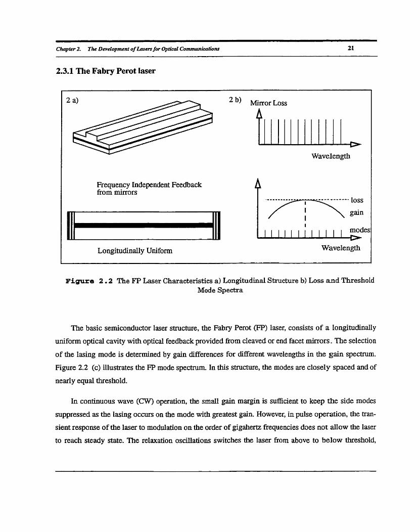
2.3.1 The Fabry Perot laser
Frequency Independent Feedback fiom mirrors
I
~ l l l l l l l l l l l gdes Wavelength
Figure 2.2 The FP Laser Characteristics a) Longitudinal Structure b) Loss and Threshold Mode Spectra
The basic semiconductor laser structure, the Fabry Perot (F'P) laser, consists of a longitudinally
uniform optical cavity with optical feedback provided fiom cleaved or end facet mirrors. The selection
of the Iasing mode is determined by gain ciifferences for different wavelengths in the gain spectnim.
Figure 2.2 (c) illustrates the FP mode spectm. In this structure, the modes are closely spaced and of
nearly equal threshold.
In conünuous wave (CW) operation, the smaü gain margin is m c i e n t to keep the side modes
suppressed as the iasing occurs on the mode with greatest gain. However, in pulse operation, the tran-
sient response of the laser to modulation on the order of gigahertz fiequencies does not alIow the laser
to reach steady state. The relaxation oscillations switches the laser fiom above to below threshold,
resulting in power being distributed to the side modes. In this case, FP lasers become multimode
devices, increasing dispersion effects and reducing the baodwidth of the fiber,
In communication systems, single mode operation and frequency stability of the source are criti-
cal factors because of the adverse effects of dispersion in the optical fiber, This is especially important
for systems that operate at 1.55 Pm, the Ioss minimum, where dispersion can stiU be hi@. High bit
rate systems require sources with SLM operation,
A variety of methods for obtiu'ning SLM control have been examined, The use of short cavity,
cleaved-coupled-cavities (c3) [12], disaibutecl Bragg refiectors (DBR) [13], and the distributed feed-
back @FB) [14] laser have been studied. The most favoured solution are DFB lasers that offer a direct
replacement for FP Iasers with additional advantages of spectral purity.
2.3.2 Distributed FeedBack laser
Periodic Index
2.3 b) Frequency Dependent Feedback
loss
A 4 A
Deviation from Wavelen,oth
gain material
Figure 2.3 The DFB Laser Characteristics a) LongitudinaI DFB Structure b) Threshold Mode Spectra
- - -
Chqpkr 2. Inc Deveiopment of Lasers for Opticd Conununications 23
The DFB laser sources that are presently used in long-haul systems offer single frequency opera-
tion under modulation. These structures were proposed by Kogelnik and Shank who developed pertur-
bation coupled mode theory to examine the DFB effect[l5]. The DFB laser devices were extensively
studied during the 1980s, and used in commercial syskms by 1990 (e.g. BNR OC-48, 2.4 Gb/s sys-
tem) .
The operation of DFB can be understood fiom the Bragg scattering from the grating which pro-
vides wavelength dependent feedback The Ii-equency dependent feedback of the grating gives a
greater cavity loss for the non-lashg longitudinal modes, aüowing for better mode discrimination. For
index coupled gratings there are, however, two lowest threshold modes that are degenerate and equally
spaced above and below the Bragg fiequency. The two symmetnc lowest threshold modes correspond
to degenerate solutions, one with standing wave peaks located at the hi@ index grating teeth and the
other wiîh peaks located at the low index grating teeth. The higher effective index of the hi@ index
peaked mode will have a longer vacuum wavelength than the center Bragg waveiength and the low
index mode wiil have a lower effective index, giving it a shorter vacuum wavelength than the Bragg
wavelength. The relative position of these two lowest threshold modes on the wavelength dependent
gain peak provides the gain difference that would determine the lasing mode of the device.
Although the DFB laser provides advantages over FP lasers, there are several undesirable charac-
teristics inherent in the structure. DFE3 devices have low yield [16] due to sensitivity to the facet phase
condition, Spatial Hole Burning (SHB) 1171, DFB mode spectra has degeneracy in the two lowest
threshold modes Cl81 and experiences mode hopping in hi& power and high temperature operation. To
examine these factors longitudinal modehg becornes necessary and has been a subject of substantial
work [4] [14] 17 11 [77l[25] [30] [3 f ] 1941.
The grating termination facet conditions criticalIy affect the longitudinal mode distribution in
DFB lasers. This end phase cannot be defined accurately because the cleave precision can oniy be con-
trolled within 0.2 pm (where the size of grating pitch -0.25 Pm). This uncontrollable device param-
eter is ?he cause for the non-unifonn characteristics between devices. The facet grating phase
uncertainty results in device yields typically worse than 50%. The final yield for packaged DFl3
devices is only 2-3 %.
CIurpler 2. The Development of Lasers for Uptkaf Commwiicationr 24
Spatial Hole Burning (SKI3) is a resuit of spatiaüy inhomogeneous depletion of carriers due to
greater stimuiated recombination in regions of higher optical mode intensities. As carriers are
depleted, the SHB results in non-linearity in the light vs. current characteristics. The dependence of the
optical mode on the facet refiection makes longitudinal SHB as random as the facet phase. The extent
of SHI3 can be controlled by the DFB grating coupling strength since the grating coupling strength
determines how peaked the longitudinal mode is in the laser cavity.
Wïth a low gain margh, the degeneracy of the two lowest threshold modes could allow mode hop-
phg. Different methods have been used to remove the degeneracy in the two modes by breakhg the
symmetry in the grating. One method is to add a phase shift (PS) tu the grating to remove the mode
degeneracy In 1976, a 7d2 phase shiffed grating was used to obtain SLM operation at the Bragg wave-
length [18]. This resulted in lasing on the Bragg wavelength in the middle of the stop band. However,
the longitudinal mode is highly peaked on the phase shift section and leads to SHB. These devices
require perfect anti-refiection (AR) coated facets to elirninate the effects of the facet reflectivity and as
a result half the optical power has to be wasted.
Besides the limitations in yield, directly modulated 1.55 pm DFE3 lasers that are currently used
in high long haul bit-rate digital transmission systems suffer fiom dispersion due to wavelength chirp
that become pronounced at high bit rates. This chirp is a slight wavelength shift, caused by the tran-
sients fiom the modulated drive current applied to the laser. The current variation causes a carrier con-
centration variation resulting in a change in refiactive index.
To elimisiate the chirp, new sources are being developed that integrate a continuous wave (CW)
high power laser source with an extemal modulator, such as Mach-Zehnder (e.g. used by Nortel) or
Eiectro-absorption (e.g. used by M&T) for 10 Gb/s sources. Since the laser light source is operated at
constant power, there is no turn on fluctuation.
The use of high power phased locked arrays to satisfy the needs for higher power is not possible
because of the poor efficiency coupling to narrow circular core fibers. Thus, improvements in higher
power for communications requires a singIe HP laser with improved design. This introduces a new HI?
Chaptkr 2. The Development of Lasers for OpCical Communuaiions 25
operation regime for DFB lasers necessary for extemal modulation where the main challenge in design
is the stroager thermal degradation in the device characteristics because of the narrower bandgap in
these devices.
Existing DFB rnodels have not included this new regime of operation. A new thermal DFB model
that inclu&s thermal self-consistency is needed to model thermal eEects for these new high power
devices. in this thesis, a mo&l for HP DR3 will be presented and applied to a Fioating Grating HP
1.55 prn DFB laser for high bit rate applications.
2.3.3 Gain Coupled laser
Many of the probIems of the DFB lasers can be improved through the use of Gain Coupling (GC)
Erom gain gratings (illustrated in figure 2.4). The use of periodic gain to produce gain coupling was
proposed dong with index coupling by Kolgenik and Shank These devices have been shown to have
superior spectral characteristics, without the yield problems of the index coupled DFB. In place of the
index grating, a periodic variation in the gain or loss c m result in mode discrimination and SLM oper-
ation. Realizing practical device structures, however, proved to be more dinicult and its development
has lagged behind the DFB laser. Reports on properties of gain coupled (GC) DFB laser have begun to
appear in literature in the last 10 years. This has much to do with how the periodic gain segments are
electrically pumped and how design consideration have to encompass the difFerent local field and gain
material overlap, subjects not previously dedt in with in any DFE3 model. Only in the last few years
have commercial GC-DFB lasers become available.
Chapter2. The Developmnt of Lasers for Optical Commwrûations 26
- -
Periodic Gain (assume uniform real index)
2.4 b) Only one lowest threshold mode.
loss
Deviation from Bragg Wavelength
Figute 2 -4 The Gain Coupled Laser a) Longitudinal Structure b) Threshold Mode Spectra
Gain coupling was demonstrated in 1982, when a loss grating was used to give the periodic varia-
tion of gain. The material gain or loss is represented by the imaginary component of material index and
coupiing results from Bragg scattering from complex index corrugations. It was theoreticaily predicted
that pure gain coupling removes the mode degeneracy that exkt for index coupling [18]. Hamasaki
showed that even the addition of ody partial gain or loss coupling was M c i e n t to break the symme-
try of the stop-band [20], The mode with peak powers in the high index gratiog with the gain material
has superior gain overlap with optical mode, hence partial gain coupled lasers Iase on the longer wave-
Iength mode, which was verified in 1989 [22]. In 1988, GaAs GC DFB lasers were fabrïcated and
observed ta have eahaaced immuaity to back re fïection compared to index coupled lasers 1231. In gen-
eral the reflection immunity is a complicated function of grating coupling and facet reflectivities. The
gain coupled devices are not sensitive to facet reflections because the intensity distribution is deter-
mined fiom the gain grating and the electtic field overlap with the gain sections. Gain coupling greatly
-- -
CIurpkr 2- The Developrnent of Losers for Optical CommunicafiO~ 27
improves yield and immunity to backscattered light. Ln 1991, the potential of increased yield was
examined taking into account SHI3 1241, The authors quantified the compromise of extemal dope e s -
ciency with the introduction of a loss grating.
The GC devices have a lower effective linewidth enhancenient factor, thereby reducing undesir-
able chirp ttirough controlling the longitudinal mode by correctiy manmg the relative phase of gain
(loss) and the index grating. For anti-phase gain and in-phase loss coupled devices, the overall increase
in couphg serves to enhance differential gain and reduce the effective linewidth factor,
An undesirable side effect unique to GC-DFB is a power dependent grating coupling strength
[95]. Above threshold, the laser could have a gain variation due to SHB and saturation that affect the
spatial uniformity of the gratings. In loss gratings, bleaching of the absorptive materials causes grathg
variations that affect mode stability and dynamic performance.
In GC structures, the gain is distributed over spatial distance on the order of the wavelen,oth of
light. On this sale , the effects of the e1ectric field interference becomes important. To mode1 the GC
coherence effects fiom including local field variation is necessary. Textbook laser theory fias been
based on the implicit assumption that the device structural spatial variation is on a length scale much
longer thaa the k i n g wavelength and thus taken spatial averaging of the photon density over many
periods to make the problem manageable. These approaches are hadequate for GC structures.
2.4 Longitudinal Laser Mode1 Development
As the longitudinal design of the laser sources progressed, rnodels have also been advanced. At
the present time, to investigate new device structures fiirther improvements in the models to include
local field and thermal effects are need.
Over the years, since Kogelnik and Shank's initial publication, rnuch work bas been done on DFB
Coupled Mode Theory ( C M . ) and DFB laser models. Originally, Kogelnik and Shank caiculated the
optical modes of penodic structures cons ide~g the perturbation fiom the weak index coupling. Today
CMT has now been extended to include above threshold lasing, more general structures with phase
Chapîer 2- The DeveIopment of Lasers for Optical Communüacions
shifts and dynamic moddation models. The CMT is restricted to weak coupling regimes. For strong
coupling, the TMM is more appropriate. By solving for the boundary conditions exactly in the device,
the TMM model is applicable to geneal index and gain coupling. The addition of coherence effects
have only been indirectly considered in some models. The addition of thermal modeiluig has been
introduced in this work
The standing wave effect was examined by Buus [771 foIIowing the earlier work of Kapron 161 for
coupled Mode examination of complex couphg due to Iaterai modal index. Using a coupIed mode
mode1 with analytical expressions for threshoId gain, and facet loss, the depth of Standing Wave pat-
tern was derived The coupled-mode solutions are restncted by the small-gain and perturbation
assumption. This work modelled AR coated, partiaily GC devices.
A tractable above threshoid model was developed by Orfanos et al. [4] based on Bjork's 1301
development of an exact numerical solution for arbitrary DFB structures through the construction of
TMM matrix and solving for the oscillation condition. Orfanos added carrier injection, and derived the
DFB threshold condition for the TMM to provide an above thresbold model. The model provided lon-
gitudinal photon density, carrier density and index profiles as weil as laser device characteristics from
longitudinal eEects. In this model only the DFB mode intemity, or photon density, was considered and
the grating was modelIed with spatially averaged sections over several periods. A DFB structure
(period of approximately 2000 teeth) was represented with 25 mesh points [4].
Dynamic TMM models have been developed using Green's function method by Makino [7 11 and
Anis[3] based on Tromberg's work[89]. In this work the dynamic model gave anaiytical expressions
for longitudinal distribution, Iasing parameters and carrier transport in partially CC QW laser.
Anis[31] was the only TMM model to explicitly consider the electric field and the associated coher-
ence effects. The photon rate eqyation fkom tbis mode1 that was applied to surface emitting lasers has
been applied to DFB and GC in this work
Similar to TMM models, numencal Tr ansmission-Line Laser Mode1 (TLLM) fiom Lowery[25]
which uses scattering m a t . to represent reflections caused by longitudinal modulation of the gain- A
m e r enhanced model was used to study dynamics and spectral characteristics of GCI.61 and
DFB[27 devices. The mode1 involves using the transmission line equivalent where the gain is repre-
C h ~ t e r 2- The Development of Larem for OpCical Communications 29
sented by lumped conductance. Once again, the model ody uses a few scattering matrices to represent
many periods of gain-loss in the laser.
This thesis presents the first elecfro-opto-thermal TMM laser model, The thermal mode1 layer has
been developed based on other works on the thermal effects in lasers. The mechanisms include temper-
ature dependent gain, re fiactive index, fiee carrier recombination [S 61, Auger reco mbination [45], lat-
eral current spreading 1331 and heterobarrier le-e [38].
The capacity of Optical Communications systems are Wted by dispersion and Ioss, To achieve
higher performance, single longitudinal mode (SLM) sowce designs with narrow iinewidth and high
power are needed.
The rapid progress of laser device designs have evolved from FP devices with simple transverse-
lateral structure into complicated longitudinal grating structures. For higher data rates, laser sources
need to operate at the long-wavelengths aear the Iow-loss and low-dispersion of the fiber medium. As
a result, the narrow bandgap active materials that are used have a consequentl y strong temperature sen-
sitivity. To achieve the spectral purity for low dispersion, longitudinal grating stmctures such as index-
coupled DFB and GC DFB lasers are necessary.
To create the next generation higber bit-rate sources, even the dispersion effects of the wavelength
chirp that results from current modulation in directly modulating the DFB devices has to be mini-
mized. Hence, high power DFB lasers operating in CW mode and ernitting in the temperature sensitive
long-wavelength range have to be developed.
To develop these new lasers, more complete 3D anaiysis is necessary not only to predict the per-
formance of devices, but also to provide insight to the underlying device physics. A complete three
dimensional (3D) electro-opto-thermal model would be the ideai tool for analysis, but presently such
numerically intensive models are not practical with current computational abiiities and are more
obscuring of physical behaviour. However, a clear picture of the essential physics of the DFE? and GC
effects can be obtained with 1-D electro-opto-thermal TMM model presented in chapter 3 in conjunc-
- - - -
Chaptcr 2. The Devefopment of Lusers for OpriCd CommunicutSont 30
tion two dimensional (2D) finite elernent analysis to study the transverse-Iateral and the Iongitudinai
efficts.
Chapter 3
Electro-Opto-Thermal Mode1 Part 1: The Transfer Matrix Method
In this chapter the electro-opto-themai Transfer Matrix Method 0 laser model for hi@
power ami arbitrary, non-uniforni longitudinai laser structures is presented. The TMM rnodel is a one
dimensional (ID) model that solves the wave equation and the carrier rate equation and includes ther-
mal self-heaîing effects. A rigorously derïved photon rate equation, originaily introduced to handle the
Iocalized gain variations in short cavity lasers has been used 131. For high power simulation, the key
mechanisms that are responsible for the temperature dependence in long wavelength lasers have been
considered. These include self-heating, temperature dependent Auger recombination, therrnionic leak-
age, free carrier absorption and the thermal dependence of the material index and gain. This new
model has the capability of modelling high power operations of DFB and gain coupled DFB that have
been difficult to treat properly by previous longitudinal models. The impact of these considerations on
the device characteristics will be illustrated in chapters 7 where îhe rnodel wïli be used with 2D finite
element analysis of the transverse dimensions to examine a novel etched through high power DFB
design and its high power performance. The gain coupling effect fiom an electric field rather than pho-
ton density consideration will also be examined in Chapter 8.
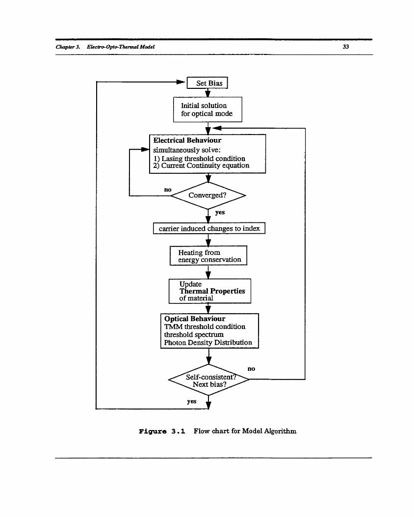
The tlow chart in figure 3.1 outiines the mo&l algorithm. F i t , the optical wave equation is
solved for the longitudinal device structure. Next the particle rate equations for the carriers and pho-
tons are solved simultaaeously to detennine the carrier concentration, and the magnitude of the photon
density. The effect of the carrier induced index change is included. The heat dissipated is caldated
and the effect of the heating on the material parameters is updated in each iteration. This procedure is
iterated until self-consistency is reached. The termination condition used is the convergence of the las-
Optical Behaviour TMM threshold condition threshold spectrum Photon Density Distribution
Figure 3.1 Flow chart for Mode1 Algorithm
In section 3.1, the theoretical development and implementation of the laser mode1 is presented.
Starting from Maxwell's equation, the description of the longitudinal optical mode behaviour is devel-
oped by decomposing the mode into forward and backward counter-propagating plane waves, Using
the Transfer Matrix Method ('T'MM), the plane waves are axially piecewise propagated through the
complex dielectric medium and the boundary conditions are matched at the corrugation interfaces.
The relation between the laser mode propagation constant, and the material parameters such as
index and gain are estabfished. Next, the TMM relations are derived and the numerical implementation
desmied, Because of the sensitive nature of the DFB behaviour to the facet condition, a derivation of
the electric field reflectivity under bias is given. Previously, only a power narrnalized treatment had
been used,
In section 3.7. 1, the threshold lasing condition is derived from the Poynting vector relation for
the photon flux. From this, the calculation of output power, the relation of the photon density to the
electric fields, and the introduction of the modified f hoton Rate Equation that accounts for the electric
field and gaia. local variations is derived, and the carrier rate equation are presented.
Next, the sirnultaneous solution of the carrier and photon rate equations is described. The particl e
and power balance gives the magnitude for the photon density and power output &om the device. Then
the carrier distribution and the index change in response to the carrier distribution are caicuiated,
The heating in the device is deterrnined from the energy conservation. From the total input power
and the optical output power, the heat dissipated in the device cm be calculated. The Thermal Model-
ling for High Power DFE3 lasers is presented in the next section.
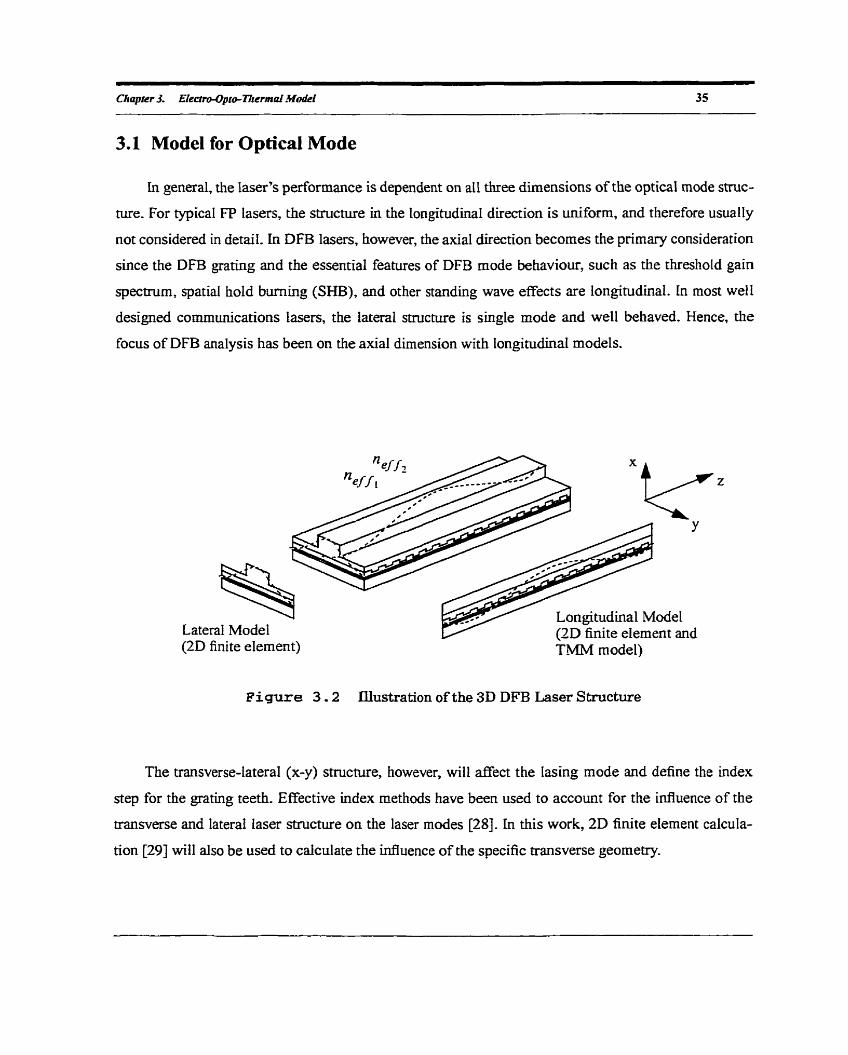
3.1 Model for Optical Mode
in general, the laser's performance is dependent on al1 three dimensions of the optical mode stmc-
tue. For typical FP lasers, the structure in the longitudinal direction is unifotm, and therefore usually
not considered in detaiI. In DFB lasers, however, the axial direction becomes the primary consideration
since the DFB grating and the essential features of DFB mode behaviour, such as the threshold gain
spectrum, spatial hold b m i n g (SHB), and other standing wave effects are longitudinal. in rnost weil
designed communications lasers, the lateral structure is single mode and well behaved. Hence, the
focus of DFB analysis has been on the axial dimension with Iongitudinal models.
Longitudinal Model Lateral Mode1 (2D finite element and (2D finite elernent) TMM model)
Figure 3 -2 Illustration of the 3D DFB Laser Structure
The transverse-lateral (x-y) structure, however, will affect the Iasing mode and define the index
step for the grating teeth. Effective index methds have been used to account for the influence of the
transverse and lateral laser structure on the laser modes [28]. in this work, 2D finite element calcula-
tion [29J wiIl also be used to calculate the influence of the specific transverse geometry.
3.2 Longitudinal Mode1
The T'MM method itself is a numerical technique of treating longitudinal optical mode by decom-
posing the domain of interest into smaU enough pieces in which variations are small or negligible and
thus is capable of providing exact numerical solutions to the Iongitudinal laser problem and is applica-
ble for arbitrary structures and coupling strengths [30]. It can handle structures which are non-peri-
odic, with large index variations resulting in gratings with strong coupling strengths [30][4]. However,
under the same n m e of TMM, many previous models have incorporated various approximate treat-
ments of relevant effects at the physical modelling level; thus render validities of varied degree.
Coupled Mode Theory is a fiequently used alternative approach which allows analytical solutions
for the DFB modes but is limited in its application by simplifjing assumptions. The coupled mode
equations are derived assuming slowly varying electric fields and considers the couphg between the
two lowest order counter propagating modes fiom smail index perturbations. The theory is restricted to
the weak coupling strength regime, with regular perïodic structures.
In the Transfer Matrix Method, the grating structure is discretized into a one dimensional series of
dielectric sections. The longitudinal field distribution in the structure is calculated from considering
plane waves propagating through this structure, being reflected and transmitted through the dielectnc
interfaces. The relation between the transfer rnatrix elements can be estabiished fkom the electromag-
netic boundary condition at the dielectric interfaces.
For completeness, the development of TMM will be described in section 3.4 but to do this, the
plane wave treatment of the longitudinal optical mode is first developed and the relation between the
complex dielectric constant with the material gain and loss is established. From this definition, the
TMM laser threshold condition will be derivcd.
3.3 Maxwell's Equations
To derive the TMM planewave description of the Iongitudinal opticai mode and the TMM thresh-
old condition for the DFB structure, following Dutta[76], we begin witti Maxwell's equations, the fun-
damental description of all electromagnetic phenornena,
Chapter 3. E i e c b Opto- Thermal Mode1 37
where 2 and are the electnc and the magnetic field vectors, and are the electric and magnetic
flux densities and 4 and p are the current density vector and the charge density sources for the clec-
tromagnetic fields.
The electric and magnetic flux densities, and B , and the electnc and magnetic fields, È and
fi, propagating in the dielecûic medium are related by the interaction of the fields and the medium.
For the case of non-magnetic materials that we are considering, the relationship can be given by,
where Eo, is the permittivity of the vacuum, P is the polarization of the medium, po is the vacuum
permeability. The curent density, 3, and the electric field are related by the conductivity of the
medium, fl ,
? = 02 Considering harmonic time variations, a more convenient complex notation c m be written as:
a n , y, z, t ) = ~ e [ È ( x , y, z )e j a r l (8)
where È is the cornplex vector amplitude which contain a spatial phase factor. With sirnilar definitions
for a and P , the complex form for Maxwell's curl Equations in dielectric medium is expressed fkom
equation (3) and (6) as,
substituting equatiom (5) and (7) into (4) gives,
To obtain the wave equation for the propagating optical field inside the laser cavity, we take the curl of
equation (9) and substitute the relation in (10) on the RHS to get an expression in terms of the electric
field and poictrization. ushg the cufl vector identity, V x (V x È) = V . (V - È) - v28 aimg
with the fact that for spatialiy uniform medium p = O , equation (3) gives V - = O. Since V - P is negligible in the cases considered, equation (5) gives V - 2 = O , so,
this c m then be written as,
is the speed of Light in vacuum. where ko = o / c is the vacuum wave number and c = - */Po"*
Considering dispersive medium, the response of the medium to the fieId excitation is not instants-
neous due to inertia effects related to the response time for the electrons and resonance absorption
effects. In steady state the response of the medium to the electric field harmonies can be relate by,
where the medium susceptibility, ~ ( w ) , is fiequency dependent and complex reflecting the phase
response. For isotropie rnediwn x is a scaiar and cm be divided into two parts,
X = X o f X , (14)
where x o , is the medium susceptibility without extemal pumping and x p , is the change in the suscep-
tibility which is dependent on the concentration of charge carriers in the active Iayer.
Substituting (13) for the electrk polarkation P in (12),
gives the time-independent wave equation,
v2È + k&È = O (16)
where the cornplex ciielectnc constant, & , is defined as,
E = E,+ jei
where the real part is,
Er = 1 + W x o I + R e [ x p 1 (18)
which consists of a background dielecûic constant of the unpumped material 1 + Re[&] and the
contribution due to pumping Re [&] , and the imaginary component is,
3.3.1 Plane Wave Representation and the Complex Propagation Constant
The essence of the mode behaviour in DFB lasers is one dimensional and hence plane waves can
be used to approximate the behaviour of the lasing modes. For plane waves polarized in the x-direction
and propagating dong the longitudinal z-axis, the electric field c m be written as:
where 2 is the polarkation unit vector, Eo is the wave amplitude and P is the complex propagation
constant. Normalizing with the wave number, gives the complex modal index, n ,
P = kon
where the real and imaghary parts of the cornplex index can be defined as,
The real part, n,, is the refractive index of the waveguide and a in the imaginary part of the index is
the attenuation constant or the net power absorption coefficient that changes with extemal pumping.
This interpretation can be seen from the fact that a governs the rate at which the intensity of the plane -012 wave (20) grows or attenuates = e . Substituting the plane wave electric field expression into the
time independent wave ecpation (16), we see that the modal propagation parameter, p, is related to
the material medium parameters n, a b y:
2 The relation between the complex dielectric constant and rehctive index is, E = n . For a << n,ko
relating the real and imaginary parts of the complex index to the material parameters gives,
Physically, the absorption coefficient a for the optical mode has three different sources. The first term
accounts for the material absorption and c m be related to carrier transparency density in the material
gain- The second term accounts for the reduction of the absorption coefficient with extemal carrier
injection. Their combined effect as a net gain, G, can be written as,
The last term in equation (25) accounts for the interna1 loss of the material. It is a combination of sev-
eral mechanisms such as fiee carrier absorption (FCA) and scattering loss. Collectively they are
accounted for through,
the net absorption coefficient in (25) can then be written as,
Having established the plane wave description of the mode and the relation that the material
refiactive index and gain-loss has on the propagation constant, we will now look at the construction of
the tramfer matrices, the TMM threshold condition for the DFB optical resonator cavity, and its
numerical solution.
3.4 Transfer M a W Method
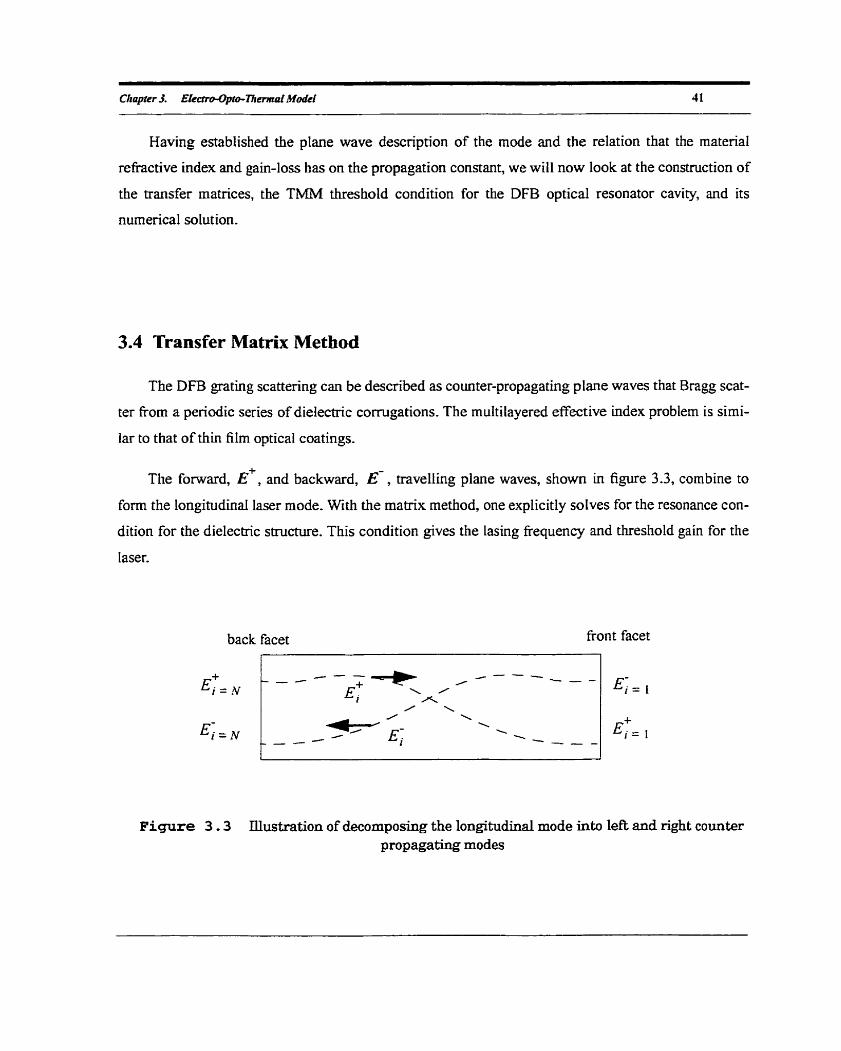
The DFB grating scattering can be described as counter-propagating plane waves that Bragg scat-
ter from a penodic series of dielectric comgations. The multilayered effective index problem is simi-
lar to that of thin film optical coatings.
+ The forward, E , and backward, Ë, travelling plane waves, shown in figure 3.3, combine to
form the longitudinai laser mode. Wtth the matrix rnethod, one explicitly soIves for the resonance con-
dition for the dielectric structure. This condition gives the lasing fiequency and threshold gain for the
laser.
back facet front facet
Figure 3 . 3 Illustration of decomposing the longitudinal mode into 1eR and right counter propagatiag modes
3.4.1 TE TMM Relations
Ln the TMM scheme, the longitudinal structure is discretized into a fixed number of sections com-
posed of uniform and interface regions between differing material index, As shown in figure 3.3, in
each section i the longitudinal mode, Ei(z) , is related to the fonvard and backward propagating
modes by,
E,(z ) = B&) + Ef (z) (29)
where E : ( ~ ) , is the amplitude of the forward wave at z and Ef (2) , is the amplitude of the backward
propagating wave at z.
3.4.2 Matrices for one period
The TMM for one complete grating period c m be described fiom the constituent TMM sections
for a penod of a DFB grating, written in terms of mat& [ap,] and [ai,,] . The TMM for the
whole grating structure can be constructed in a similar manner.
Considering one section i of the grating, the forward and backward propagating waves in the
i + 1 section are determuied fiom the left and right propagating waves in the i section expressed in
matrix form would be,
where the matrix elements are determined fkom Maxwell's equations and the boundary conditions that
must be met at the dielectric interfaces. Note that in this convention the indices i starts from the desig-
nated output facet on the right hand side,
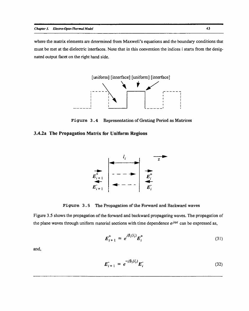
[unifonn] [interface] [uniform] [interface]
Figure 3 - 4 Representation of Grating Period as Matrices
3.4.2a The Propagation Matrix for Uniform Regions
Figure 3 . 5 The Propagation of the Forward and Backward waves
Figure 3.5 shows the propagation of the forward and backward propagating waves, The propagation of
the plane waves through uniform material sections with tirne dependence ejoi can be expressed as,
-- - - -
Chapter 3. E I e ~ p r + 7 7 1 e m o l Modei 44
on,,. ai where the propagation constant for each section i is given by Pi = - + j- , where n,,. is the
Co 2 material index and ai is the gain or loss for the uniform region and fi 1s the distance. Re-written in
3.4.2b The Interface Mat ix Relation
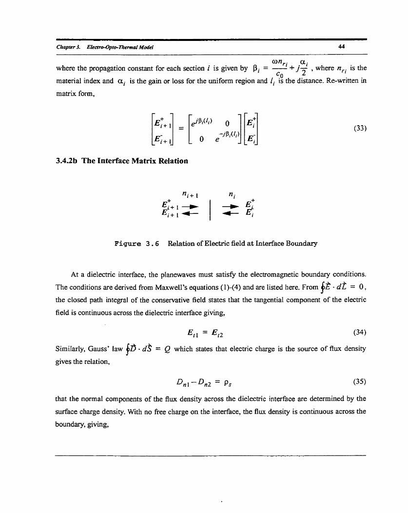
ni+ 1 ni
Figure 3 . 6 Relation of Electric field at Interface Boundary
At a dielectric interface, the pIanewaves must satis@ the electromagnetic boundary conditions.
The conditions are derived from Maxwell's equations (1)-(4) and are listed here. From $2 d t = 0,
the closed path integral of the conservative field states that the tangential component of the electric
field is continuous across the dielectric interface giving,
Similarly, Gauss' law - d? = Q which states that electric charge is the source of flux density
gives the relation,
that the normal components of the flux density across the dielectric interface are determined by the
surface charge density. W1th no fiee charge on the interface, the flux density is continuous across the
boundary, giving,
for the electrïc fields. For normal incident TE and TM polarized planewaves En = Enz = 0.
Ampere's circuit law, $fi - d t = I , gives the tangentid relation for the magnetic field across the
boundary in terms of the surface current, K,
in the cases that are considered, t fie surface current is K = O so,
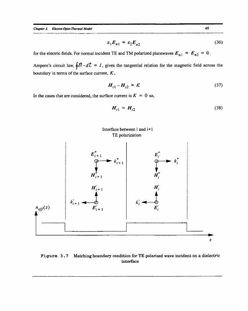
interface between i and i+I TE polarization
Figure 3 .7 Matching boundary condition for TE polarized wave incident on a dieIectric interface
Figure 3.7 illustrates TE polarized waves at an interface. The electric fields are illustrated as pointhg
out of the page and is tangential to the dielecûic interface of the segments. From the boundary condi-
tions (34) and (38), the tangential component of the elecaic and magnetic fields are continuous. Satis-
Qing the boundary condition by equating the total electric fields in regions i and i + 1 gives,
- H : + , + w ~ + , = - ~ f t ~ f (40)
For plane waves, the electric field and the magnetic field are related by the impedance of the medium,
Satisfying the magnetic boundaq condition (40). using expression (41) and takiog into account tbe
sign Born the vector directions we get the relation,
so the boundary conditions gives the pair of equations, relating the field across at the interface.
E;,+E;+, = E ~ + E ;
+ + n i + l E i + l - n i + l ~ ~ + l = niEi n ni^;
rewriting (44) and (45) in ma- form gives,
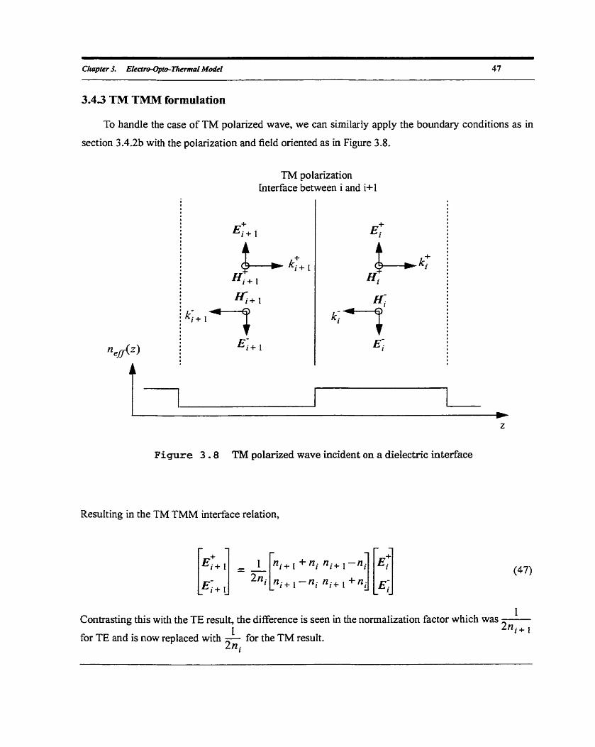
3.43 TM TMM formulation
To handle the case of TM poI;il.ized wave, we can similarly apply the boundary conditions as in
section 3.4.2b with the polarization and field oriented as in Figure 3.8.
TM polarization Interface between i and i+l
Figure 3 - 8 TM polarized wave incident on a dielectric interface
ResuIting in the TM TMM interface relation,
1 Contrasting this witll the TE result, the difference is seen in the normalization factor which was -
1 2ni+ r . - for TE and is now replaced with 2 for the TM result.
Zni
3.5 End facet reflectivity condition
The DFB mode solutions are very sensitive to the optical oscillator boundary condition. This is
also reflected in the low yields of approximately 50% due to the phase uncertainty of the grating termi-
nation from the cleaving process 1161. Consequently, proper treatment of the facet condition for the
optical cavity is critical and has to be carefully derived Previous models that model the field intensity
consider only the power nonnalized refi ectivity for photon density rather than the electric field refiec-
tivity 141. In this section, the power reflectivity is shown to be improper for a field TMM model which
is necessary for treating Iocal field effects such as intefierence and the correct electric field reflectivity
matnces are given. It will M e r be shown that to correctiy represent the reflectivity and account for
the index changes under injection, the reflectivity is best modelIed as an equivalent effective extemal
index,
n a) actual facet coating air
index structure + * m m - - b) proper reflectivity matrix for electric fierd n -
4---
c) equivaIent effective index for refiectivity
Figure 3 - 9 The facet boundary condition: a) the physical mirror structure b) reflectivity matrix representation c) effective index method for the b i s .
3.5.1 Field Reflectivity
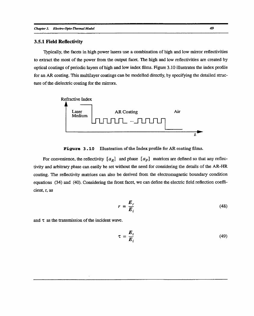
micaiiy, the face& in hi& power lasers use a combination of high and low mirror refiectivities
to extract the most of the power f3om the output facet. The high and low reflectivities are created by
optical coatings of periodic layers of high and Iow index films. Figure 3.10 illustrates the index profile
for an AR coating. This multilayer coatîngs c m be modelled directly, by specifying the detailed struc-
ture of the dielectric coating for the minors.
Refiactive Index
Laser AR Coating Air Medium
Figure 3 -10 IUustration of the Index profile for AR coating fiims.
For convenience, the reflectivity [aR] and phase [ap] matrices are defined so that any reflec-
tivity and arbitrary phase can easily be set without the need for considering the details of the AR-HR
coating. The reflectivity matrices can also be derived from the electromagnetic boundary condition
equations (34) and (40). Considering the front facet, we can define the electnc field reflection coeffi-
cient, r, as
and 2 as the transmission of the incident wave.
Front Facet on RtIS
Incident ET
Laser Medium
out
- Transrn i tted
Figure 3 .11 The Reflectivity for the Right Facet
Calculating the reflectivity of incoming wave, and applying the boundary conditions (34) and (37)
again:
Ei + Er = El
Hi-& = Hf
equation (5 1) c m be re-expressed in terms of the electric field,
- E ninEi-ninEr - L
Solving equations (50) and (52) gives the relation for the field reflection coefficient as,
where r is positive for high index to low index and undergoes a sign change ( x phase SM) from low to
high. Similarly, adding equation (52) and the product of ninand equation (50) gives, the field transmit-
tance, T ,
Now, expressing the interface relation derived in (461, in terms of the field reflectivity (53) the bound-
ary conditions @es,
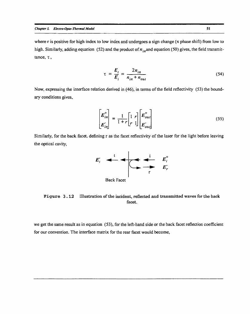
Similarly, for the back facet, defining r as the facet refiectivity of the Iaser for the light before leaving
the optical cavity,
Back Facet
Figure 3.12 Illustration of the incident, reflected and transmitted waves for the back facet.
we get the same result as in equation (53), for the left-hand side or the back facet reflection coefficient
for our convention. The interface matrix for the rear facet would become,
- - (no,, + n,)
%ut 2nour EL1
which when re-expressed in terms of the refiection coefficient delined by equation (53), gives:
These results differ from the power normaiization factor 1
used in [4]. The power normalized
result ignores the phase in the reflectivity matrix is clearly inconsistent with the
electromagnetic boundary relations.
The p a s modeIs, dealt with the photon density and hence derived the reflectivity matrix for
power. From energy conservation, + I = 1 where R is the reflectance or the fraction of energy
reflected and T is the energy transmittance- From conservation of energy, they arrive at, I = L -
and hence, they set the transmission coefficient as 171 = JFR.
Electric Field Mode1 Previous Intensity Mode1
T = 1 + r at the front 2 = 2-1- attheback
R + l = 1
7 = ,,/= at the fiont and the back
where Zo and Zi are the input and output material impedance given y Zi = JGi
However, cornparhg with boundary condition (46) has shown that the intensity and field coeffi-
cients are not simply related by, I = lzI2, but rather must include the impedance of the medium,
since the boundary condition across the interface. The Tmnsmittance is defined as:
' incident
where Zi = */Gi and Zr = ,,/Zr. From the defmition of the transmission coefficient, T, from
(54), it is reIated to the intensity transmittance factor by,
The reflectivity matrices defived in (55) and (57) can be seen to satisfj the interface matrix relation
(46) whereas the previous power normalization expression does not.
A m e r complication arises when the device is biased. The electric field facet reflectance is a
function of the complex dielectric constant in the laser medium and as a result, the complex mirror
reflectivities are curent dependent. Reflectivity matrices derived with a fixed facet reflectivity would
not have this b i s dependence. To handle the reflection correctly under bias, it is necessary to calculate
the irnaginary contribution explicitly, accounting for the index changes with m e n t by using an equiv-
alent boundary index just outside the laser facet.
To represent the changes in the complex dielectric constant in the reflectiviw matruc, an effective
outer inde.x has to be debed for a specified reflectivity, r . B y inverting the re flectance relation (53),
For the refiection coefficient cdculation an equivaient effective outer index is required to give the
proper complex reflection coefficient to be used. With this scheme, the travelling plane wave reflectiv-
ity is calculated explicitiy at each bias with the correct current dependent reflection and phase.
3.52 Phase
Figure 3.13 Convention for the facet phase.
The end facet phase as a result of the fractional part of the period that remains fkom the cleaving
process has to be accounted for. The phase is known to have a critical effect on the modal behaviow
especially in the case of hi@ mirror reflectivity. The phase shift at the facet can be defined using the
3.6 TMM Threshold Condition for the Longitudinal Cavity
Any structure, AT , can now be represented by the matrix relation: [ 1
Figure 3.14 The formation of the representative matrix for the whole structure h m the TMM elements.
1 r 7
w here
The relation for the complete laser cavity is then represented with the A~ rnatrix,
For periodic structures where a unit ce11 is repeated throughout the structure, the matrix element of
[ A ~ ] can be analytically detemillied from the eigenvaiues of the unit ce11 [30]. However, generally in
Iasers where there are non-unifonn carrier concentrations, the index profile of the oscilIator is non-
periodic and the matrix elements have to be constmcted.
Following Bjork and Nilsson [30], the lasing condition c m be introduced by viewing the Iaser cavity +
as an amplifier with input, Ebrrck, and no backward propagating reflected wave, Ehack = 0 , the
amplification is expressed by,
The Iasing condition, occurs at the osciIlator resonant condition, with infinite amplification:
The matrix eiements are a function of the propagation constant, which is related to the tiequency, and T
the gain or l o s of the mode. The mots of the maaix element A (f, alh) give the frequency and
threshoId gain for the device.
DFB at a=a& freq=199.62-200.38THz
0.30
Figure 3.15 Complex plane trace for matrix eIement as Bequency and ath is changed
T In Figure 3.15, the locus of the manu< elernent A (f, ath) is plotted in the complex plane as a
function of the frequency for dflerent net gain parameters for the FP oscillator and at threshold gain
for the DFB device structure. As the frequency approach the mode fiequency and the gain approach
the threshold gain, the traces approach the otlgin.
For the FP structure, the locus rotates counter clockwise as the fiequency, f, is increased As a
approaches the threshold value of 34.7 cm-', the locus lies on top of the imaginary axis. The fkequen-
cies at each origin crossing corresponds to a FP mode.
For the DFB structure, the trace is symmetric about the real a i s . The lobe on real axis corre-
sponds to the Bragg fkquency and the two degenerate DFB modes correspond to îhe ongin crossings
rnoving clockwise and counter clockwise fÏom this lobe. The anow indicates the direction for increas-
ing tiequency. For a not equal to ath the locus does not cross the origin.
L
wavelength [pm]
Figure 3 -16 The calcuiated DFB transmission spectra
The device operates at the lowest threshold gain mode in the threshold mode spectrum. The solution
for the roots provide the lasing fkequency and threshold gain for the device. By varying the wave-
length, figure 3.16 shows the calculated transmission spectra for the DFB structure.
3.7 Electric Field vs. Average Photon Density
From the lasing mode fiequency and loss, the relative electric field intensity in the whole structure
is known and c m be extracted fiom the matrix elements. From the ma& elernents for the forward and
backward propagating waves, the relative photon density in each section i in the cavity at an arbitrary
point z can be calculated.
Figure 3.17 The Calculation of the Longitudinal Photon Density from the Matrix Elements.
The forward and backward waves can be calculated fkom,
where
From this, the relative electric field is known eoom the matrix elements. The photon density in the klh
section is proportional to the electric field intensity and cm be obtained by,
where P,,, is the photon density normalization factor and f is the relative photon distribution and
is given by:
The absolute value of the photon density is specsed by the nomabation factor, Pnom, that is deter-
mined from the self-consistent solution of the photon and carrier rate equations. Re-expressing in
terms of matrix elernents in (69) gives:
3.7.1 Modified Photon Rate Equation
The normalized photon rate equation, previously used for surface emitting lasers [3], was used to
provides the k ing condition for above threshold conditions in the TMM rnodel. Follo wing 131, this
local field rate equation will be derived from the Po ynting Theorem which describes the power flow for
the electromagnetic field, From this the longitudinal photon distribution and the power out of the laser
are determhed. From the Maxwell's equations we look at the complex Poynting vector,
1 P = - E x H * 2 (74)
to examine the power balance condition, for the power generated in the structure with the power loss
from the end facets of the device. The divergence of the Poynting vector is taken, and the vector iden-
tiv,
V - ( E x W * ) = H * - ( V x E ) - E - ( V X H * ) , (75)
is used Re-writiag Maxwell's curl equations in complex phasor form to include the comrnon time-
dependence ejai gives,
V x E = - j o B (76)
V x R = j o D (77)
In equation (77) J = 0 since there is no net charge density in the rnedtum. Substituthg into (75) and
applying the divergence theorem gives,
the power balance for a volume V with a surface, S. The real part of the complex Poynting vector rep-
resents the power gain or loss in the volume and the imaginary component of the complex Poynting
vector represents the stored energy in the field, Taking only the real part of (78), we see that the first
t e m on the RHS is imaginary and excluded since B = poH where po is real. The only contribution
to the real component on the RHS is from the imagioary part of D* = (&El* in the second term
which reduces equation (78) to,
where imaginary component of the dielectric constant, E i , is given in (19). Substituting the imaginary
part of the dielectnc constant with the absorption coefficient fkom (25) gives:
the power flow out of the IongitudinaI z-direction becomes,
Tg - a 2
aEojnr(-)l~l 2d v ~ J R ~ ( E x H*) - fida = - 2 ko
The power flow out of the two output facets,
2 [ R e ( E x H*)Ifront + [ R e ( E x H * ) l b r r c k = c ~ ~ l n ~ ( ~ g - ~)IEI dz (82)
where the confinement factor, T , is derived fiom the weighting of the gain with the electric field distri-
bution in the x-y plane. Simplifying, the threshold condition becomes,
where r is the optical confinement factor, g(z) is the gain distribution dong the longitudinal direc-
tion, n,(z) is the effective index distribution dong the laser cavity, a is the intemal loss, E+ and E-
are the forward and backward propagaîing components of the field while the subscript 'out' denotes
the output facets of the laser. Equation (83), is an expression of energy conservation for the device.
The right hmd side of equation (83) represents the normalized power ernitted while the left hand side
represents the normalized power gained in the structure. Normalizing this for the output power f?om
the fiont facet, and discretizing it for T'MM numencal calculation, we have,
i = 1
This rate equation includes proper eeatment of the coherent interference effects of the electric field-
Previous tram fer rnatrix models for DFB lasers (Le. [4]) have universally used spatially averaged field
intensities, to calculate the gain and loss. Physically it is the electric field that interacts with the mate-
riai, hence, the intensity treatment is improper. For devices as the FP laser, where the gain matenal is
uniformly distnbuted dong the laser cavity, the difference in the result is small. However, for VCSEL
and GC-DFB where the gain-field overlap changes abruptly on the order of the field wavelena@, the
interference effects can make a significant difference.
3.7.2 Output Power
The output power from the field exiting the optical cavity from the Poynting vector,
where the time-average power flow is given by,
2 where (S) is the average Poyoting vector or the irradiance given in the uaits of [ W / m ] . For plane
waves in a dispersiodess medium this reduces to,
The output power calculated from the electric field,
where n, is the refractive index, c is the speed of light in vacuum and &, is the material permeability
multiplied by the cross-sectional area of the outgoing mode. The factor of 1/2 comes nom the time
average over a perïod.
3.8 The Carrier Rate Equation
To cornplete the laser model, the relation between the rate of change of the photon density, rate of
change of the charge carriers and current injection has to be established This relation comes fiom the
carrier rate equation which incorporates ail the rnechanisrns by which the carriers are generated and
Iost inside the device.
in its geneml form, the canier-density rate equation is given by,
where iV is the carrier density. The fist term describes the rate of carrier d i m i o n with D being
the diffusion coefficient. The second term gives the rate that carriers are Uijected into the active layer,
where q is the electron charge, and d is the active layer thickness. The last term R ( N ) refers to the
radiative and non-radiative recombination processes. In general, there are two current continuity equa-
tions, one for the electrons and one for the holes. With the assumption of charge neutrakity condition
the two equations are inter-related and it is sufficient to consider just the rate equation for the electrons.
Carrier diffusion in seiniconductors result fiom intraband scattering and should generally be con-
sidered. For longitudinal modelling the importance of diaision has not been established, but such dif-
fusion is expected to be small because the grating segments that are considered have relatively srndi
dimensions compared to the diaision length of the carriers which would result in carrier distributions
that are relatively flat. Hence, the contribution ffom diffusion c m be neglected.
In the steady state case, * = O , eqyation (89) simpMes to, at
For the current that reaches the active region, the steady state carrier rate equation accounts for the car-
rier consumption in the processes of radiative and non-radiative recombination- By separating out the
leakage current and explicitly expressing the recombination terms gives,
J = qd(R,+R,+R, ,+Rs, )+J,+J, , , , (91)
where, Rd, and Raug are non-radiative recombination rates frorn defects, the auger process and Rsp
and R,, is spontaneous and the StimuIated recombination rate respectively. Re-writing (93) to express
the carrier dependencies, @va,
A brief description of each tenn will be given below.
3.8.1 Defect and Surface Recombination
The k s t order carrier dependence expresses the non-radiative recombination that results from defects
in the material and the surfaces. Defects exist in the laser from a number of factors that produce recom-
bination states, including the materiai growth, aging and stressing of the device. The surfaces defects
in the Iaser are created Born the cIeave facets, and the heterostmcture interfaces and also act as non-
radiative recombination centers. The coefficient for non-radiative recombination from defect states, 1
A,,, is determined kom the inverse of the non-radiative lifetime for the traps, - , where T, in prac- 2s
tice is usualiy a phenomenologicai fitting parameter.
3.8.2 Spontaneous recombination
The electrons and holes natmdly recombine with a spontaneous lifetime, as a result of induced
perturbations fiom vacuum fluctuations. The recombination rate is dependent on the availability of the
carriers and is rnodelled as a bimolecular recombination rate.
3.8.3 Auger Recombination
Auger recombination is a non-radiative recombination process that involves a three particle inter-
action, whereby carrier coliision, for example 2 electrons, induces electron-hole recombination for one
particle but rather than giving up the transition energy to a photon, the energy is absorbed by the sec-
ond particle in the collision. This mechanism is strongly dependent on the carrier concentrations and
on bandgap and hence is signifïcant in narrow bandgap devices and hi@ temperature operation. ft is
attributed as the cause for the poor thermal performance of long-waveleagth semiconductor lasers. A
more detailed discussion of the auger process and its temperature dependence will be presented in the
Thermal Mode1 section.
3.8.4 Stimulated Recombination and Modal Gain
The stimulated recombination term in equation (9 1) represents the rate that carriers recombine to
generate photons by the coherent emission of light. The stimuiated emission rate is given by,
c where, vg = - is the group velocity, Gi is the modal gain, and Pi is the photon density. The stirn- n i
ulated recombinhon can be caldated directly from the elecaic field, where,
Previous TMM models ignored the interference effects in (93). This is appropriate for traditional laser
structures, but for non-uniform gain structures this is not correct and becomes significant.
The matenal gain results from the interaction between the material and the electric field and
hence includes coherent effect. as standing waves [31]. in section 3.7. 1, it was shown using Poynt-
hg's theorem that the rate of change of the local energy density is related to the local electric field
stren,otii, NormiiIiiiing this with the total energy in the stored in the field, the modal gain and the mate-
rial gain can be related by,
where g is the materîal gain, ( G) is the modal gain, E is the transverse component of the elecaic
field Using the matenal gain in the rate equation and includùig the field interference effect, the expres-
sion in the carrier rate equation becomes,
3.8.5 Lateral Spread and Thermionic leakage current
The lateral spreading accounts for the leakage current that by passes the lasing region. Thermi-
onic Ieakage current accounts for the current that overflows the Iasing region and energeticaliy over-
cornes the confinement fiom the heterojunction. The temperature dependence of both these
mechanisms wiU be discussed in the aext section.
3.9 Material Refractive Index and Carrier Concentration
In response to the carrier injection, antiguiding occurs in the dielectric medium due to the plasma
effect resulting fiorn canïer population and bandgap changes from injection.
The carrier induced index changes can be grouped hto three main categories: 1) Band filling
(Burstein-Moss effect), 2)Bandgap Shrinkage and 3) Free carrier absorption (commonly known as the
plasma effect) 1321. The overd combined result of these effects result is a decrease in the refkactive
index and c m be represented by a constant. The change in the effective rehctive index in segment i is
caiculated fiom the change in carrier concentration,
b ias O dn ni = ni + T-Ni
dN O dn
where ni is the complex index without injection, r is the confinement factor, - is the rate of dN
change in the refiactive index with carrier conceniration and Ni is the concentration of injected carri-
ers into segment i. For 1.55 pm InGaAsP the calculation of the rate of change of the refractive dn 3 3
index on the carrier concentration, - has a value of -1 -8 x 1 0-20 cm to -2.8 x 10-~' cm . dN '
With the new index profile in response to the carrier concentration re-distri'bution, a new photon
distribution will result. The photon rate equation (84) and carrier rate equation (92) are solved simulta-
neously for the photon density power norrnalization, P,,, and the carrier concentration, Ni in each
section. The i terative solution gives the photon and carrier distributions for the longitudinal structure.
The heating in the device is cdculated from energy conservation and is described in the next sec-
tion. The temperature dependence in parameters are introduced a self-consistent solution is caiculated
at a given temperature.
In this chapter, the optical and electrical layers of the electro-opto-thermal model have been pre-
sented. hprovements over previous models that had used a field intensity model that was justifiable
for traditional laser structures to a model that includes coherence effects that are necessary for new
generation devices that have spatial variation of gain on the order of the wavelength of light. To include
the field effects, a modified rate equation that was previously derived for VCSELs was used and the
appropriate electric field boundary condition rather thaa the commonly used intensity boundary condi-
tions. The previously used averaging over several periods of the grating in traditional rnodels has been
replaced with detailed meshing of the longitudinal structure that is necessary to properly define the
electric field
The carrier rate equation has included coherence in the stimulated recombination terrn and tem-
perature dependence in tems that will be discuss in next section.
The self-consistent model has been generalized such that it is able to solve for arbitrary structures
that are periodic or non-periodic, and have composite cavities, and arbitrary de finition for the current
injection,
Chapter 4
Electro-Opto-Thermal Model Part II: Thermal Model for High Power 1.55 pm laser
La CW operation, the maximum output power fiom high power laser is m t e d by thermal run-
away. The strong temperature sensitivity of the performance of long wavelength quaternary (Q) lasers
has been weil documented and been the subject extensive experimental and theoreticaï work. The
strong temperature dependence at long-wavelengths is a consequence of the narrow band gap of the
device. The factors that detennine the high power performance of the laser are, the thermal resistance,
temperature dependence of the threshoid curent, temperature dependence of the efficiency and the
electrical resistance.
In the pst, it has been estabhhed that the mechanisrns responsible for the increase in threshold
curent in long-wavelength quaternary lasers are temperature dependence of gain function, Auger
recombination 1431 and thermionic carrier leakage over the heterojunction 1371 [38]. More recently, the
importance of the intemal loss in the SCK of QW lasers has been shown in devices with electrostatic
band-profile deformation [56]. This effect h a been shown to be a more dominate mechanism at high
temperatures.
The thermal TMM model includes: the thermal detuning of the gain and the lasing mode by con-
sidering the gain and wavelength shift with temperature; the temperature dependence of the non-radia-
tive recombination cunents Erom thermionic leakage; Auger recombination and temperature
dependent absorption loss; the heat generation and heat dissipation Eorn the specific material and
device structure,
4.1 Thermal Detuning
A themal characteristic unique to DFB lasers is the DFB thermal detuaing of the gain peak As a
consequence of the DFB mode degeneracy, the detuning or placement of the DFB stopband relative to
the gain peak is an important design consideration which determines the gain ciifference and SMSR for
the lowest order Bragg modes in the DFB laser specbnim, As the temperature increases, the material
gain peak decreases in value and shifts to longer wavelenOaths due to bandgap shrinkage with tempera-
ture. The wavelength of the longitudinal model also increases as a resuIt of the increase in the refÏac-
tive index with temperature. The rate of index shift is slower thao that of the gain peak shift, For 1 -55
Pm, the gain peak shifts of 0.7 nrn/'C have been reported. The 1.55 pm DFB longitudinal mode
shifts at 0.1 nm/O C . As the gain s p e c t m moves relative to the DFB spectrum, the gain differences
between the Iasing and lower gain side mode changes and mode competition c m occur.
left mode preferred
degenerate right mode preferred thermal DFB shift
0.1 nrn/'C
thermal gain peak shift 0.7 nm/OC
Figure 4.1 Illustration of the gain aad DFB wavelength shift with increasing temp erature.
4-1.1 Gain Mode1
A parameterized materiai gain c m e s was used for efficient access in the numerical iteration. The
gain is parameterized as a function of temperature, wavelength and carrier concentration. A general
microscopic gain model that has previously been developed was used to calculated the curves for
parameterization and includes the effects fi-om materiai group, composition, strain, strain-compensa-
tion, bulk, quantum well and barriers effects, and bandgap shrinkage. The detailed model used is
descriied in [94]. The gain function g@,N,T) is fitted to curves of the form,
where we assume the typical logarithmic fonn for the QW gain expression w
temperature dependence for the parameters go and N o .
(98)
ith added wavelength and
Gain Coefficient
The temperature and wavelength or photon energy dependencies of the gain coefficient can be repre-
sented with parameterized fitted curves. The form of the gain coefficient fitting function, go , was
obtained b y fitting the high energy absorption tail of the gain curve and including a 'Fermi-Dirac' Like
factor to give the increase in gain at low energies at the band edge. The fit function was defined to be,
where T is the temperature, a(T) , b ( T ) , c (T ) , d ( T ) , e (T) , and f (T) are fitting parameters, Eph
is the photon energy. The curve is fitted for energy at a specific temperature. The parameters a , 6, c ,
d , e and f are in turn fitted to have a linear dependence with temperature. To first order, the parame-
ters' temperature dependence can be approximated to be linear,
The values from the fit h c t i o n are compared with the calculated gain coefficient in figure 4.2 which
shows the parametrized gain curves with the Luiearized temperature dependence in the coefficients
- -
applied over the expected operating temperature range of the laser of 20 O C - 1 10 OC. Figure 4.2
shows that the fitted curves reflect the same temperature behaviour as the gain curves., with good fits
for the band gap cut off and the absorption tail. At 1 10 OC a srnall difference in the gain peak ampli-
tude can be seen, This is a resuIt of taking only a first order thermal dependence in the parameters. A
higher order dependence could be used but the result wouid not significantly enhance the accuracy of
the results nor add M e r physical insights.
0.70 0.80 0.90 Photon Energy [eV]
Figure 4.2 The parameterized gain curves compared with the calculated gain curves from model [Ml.
The carrier transparency has dso been fitted to a first-order linear temperature dependence,
N,(T) = N o + N I - T (101)
The gain mode1 and fitted curves have been compared with experimentally collected gain data. The
measured gain results show the same physical trends as the calculated gain curves.
4.1.2 DFB thermal wavelength shift Mode1
The change in the DFB lasing wavelength with temperature, h(T), results fiom the change in the
material index with temperature- The main contribution to the index change is band filling fiom the
carrier re-distribution with temperature in the Fermi-Dirac distribution. The result is an increase in the
refractive index around the wavelength of maximum gain with increasing temperature. There is also a
change in the grating index from thermal lattice expansion but this value is very srnall and is less of a
factor.
4.2 Lateral RWG Leakage
Figure 4 .3 Diagrarn illustrating the calculation of the lateral current spreading
The increase in the lateral leakage with temperature significantly hcreases the heating in the
device. The leakage is structure specific, but the temperature dependence for this effect can be
addressed. Following the procedure from [333 the lateral leakage currents away fiom the current
injected into the active region c m be & h e d as:
1, = I, + 21, (1 02)
where 1, is the total injected current, I , is the uniform vertical component of the current that flows
into the active region and Io is the lateral current that spreads in the y direction. The lateral Ieakage
current was examined by modelling the vertical junction as a series of diodes in parallel. The lateral
differential m e n t in the y direction between y and y+dy can be expressed as:
-dly = LJs(exp(PVy)- 1) -dy
The voltage drop across the layer -d Vy is given by:
-dVy = pylydy
giving the differential equation, for P V y » 1
The solution of (105) is,
L where Io = - . The lateral current between y and y+dy Born (106) gives:
P P # O
Applying the boundary condition of known uniform current under the ridge at y = O
and an effective ridge width of W gives the relation
for the lateral leakage and the active region currents, where P = 4- , q, n, ks and T are the electron nk,T
charge, non-ideality constant, Boltzmann constant and the t e q e r a h e respective1 y. Substituling into
equation (102) gives the quadratic relation
2 AI, + 21, - 1, = O
where
and py is the lateral resistivity, L is the len,@h of the device and d the thickness of the material. Solv-
k g for Io gives the laterd leakage current for a given bias current,
Substituthg in the temperature dependence for the increase in lateral leakage gives:
4.3 Thennionic Leakage Current
The thermionic hetero barrier leakage is a non-radiative recombinatio n carrier loss which
increases exponentiaily with temperature, Thermionic Ieakage is a consequence of the thermal distri-
bution for the charge carriers that populate the higher energy States that are energtic enough to escape
the carrier confinement in the active and separate confinement heterostructure (SC@ (see Figure 4.4
). The magnitude of the overflow current is dependent on the doping and thickness of cladding layer.
The heterobauier le-e is known to be a major loss mechanism for small heterobanier heights. For
properly designed 1.3 - 1.55 pm the leakage is thought to be smaU (10-30%) [34]. However, the expo-
nential temperature dependence makes tbis an important canier loss mechanism at high temperatures
1351-
Figure 4.4 schematicdly shows the band structure in the thennionic leakage calculation. With the
assumption of quasi-equilïbrium between the active and cladding regions the quasi-fermi level Ef is
flat through this region. In heavily doped P-InP cladding structures most of the band gap discontinuity
in the conduction band.
Case A, Uustrates the simplified case of diaision limited leakage. For a well designed device, the
doping is suficieat so there is no field dependent band bending and hence the band structure is flat. In
more realistic devices the shape of the transverse band profile is dependent on the doping and the bias.
It bas been shown that the cladding doping is often underestimated making thermionic leakage an
important factor [35].
Thermionic leakage appears for both the electrons in the p-cladding and holes in the n-substrate
with jL = j,, + j,,. However, the diffusion length and mobility of the electmns are larger, malcing
the electron leakage considerable larger than the hole leakage, so, only the electron leakage needs to be
considered
To calculate the thermionic leakage, the drift-diaision equation for the carnier is solved in the
cladding for the leakage current out of the contact, It is assumed that the electrons in the active-SCH
region is in thermal equilibrium with the electrons in the cladding region making the fermi level flat
and continuous across the boundaries. The amount of caniers escaping to the cIadding region is deter-
mined ffom the fermi-levet location that is speczed by the active region carrier concentration.
Figure 4.4 ilIustration of thermionic leakage from the QW band structure
Leakage Current Calculation
The calculation of the leakage current for Dias ion and Drift foIIows [37] and [38]. The proce-
dure calculates the current flowing to the contact fkom the cladding layer £tom the minority carrier den-
sity in the cladding at the GRiN interface and solving the minority drift and diffusion current hough
the cladding. From the Dnfi-Diffusion equation (following Dutta [37]), solving the minority carrier
rate equation in the p-cladding in the presence of an electric field,
with the carrier rate equation,
where a is the mhority carrier lifetime. The resulting minotity cauier leakage current becomes:
where q is the electronic charge, xp is the P-cladding layer thickness, Ln is the minority electron dif-
fusion length,
D, is the miwrity electron dinusion coefficient, given by
p, is the eleciron mobility, kB is Boltzmann's constant, and T is the absolute temperature. Nb is the
concentration of the minority electrons at the edge of the P-cladding layer and z is the characteristic
length of the drift leakage, given by,
where op, is the electrical conductivity of the p-cladding layer and J,,,,[ is the total current density
into the active region.
Bulk Active Region
For bu& material with 3D density of states, the position of the fenni level can be determined fiom
the carrier concentration in the active region. The fermi-level for &generate semiconductors c m be
calculated b y inverting the carrier concentration expression. Using the JO yce-Dixon approximation
1391, the position of the fermi level, Efc, in the bulk active region can be determined fiom:
where the first four coefficients are: A l = 3.53553 x IO-', A2 = -4.95009 x 10 -~ .
A3 = 1.48386 x lo4, A, = 4.42563 x 10"
Quantum Well Active Region
As the active region heterostrticture confinement is made smaller approaching the deBroglie
wavelength, quantum size effects (QSE) appears due to the confinement of carriers in the transverse
direction. The confined eIectrons in the potential weII become a 2D system. A review of the properties
of the QW laser can be found in [40].
1.55pm
Figure 4.5 The band structure parameters for the MQW thermionic leakage
An illustration of the MQW-SCH band structure that will be exarnined is s h o w in figure 4.5 for
the cakulation of the therrnionic Ieakage out of the MQW and SCH to the top P-contact in the clad-
ding. The heterojunction discontinuities in the conduction band and valence band for InGaAsP mate-
rial are [4 13,
For heavily doped cladding regions the bandgap disconrhuity for the cladding is approximately epal
to AEg . The carrier concentration in the active region is determined from the threshold condition to
achieve lasing. Assuming thema1 equilibrium, the quasi-fermi Ievel will be fiai throughout this region-
To locate the fermi level, is it necessary to cdcdate the QW energy levels and 2D-DOS as weii as
the unconfined buk 3D-DOS in the region above the well. The energy levels in the quantized trans-
verse x direction are calculated by soIving Schrodinger's equation for the finite one-dimensional
potential welI, inside the well (O I x I d ) ,
outside the well ( x I O, x 2 d ) ,
where is the electron wave fùnction and V is the depth of the weli in the coriduction band. Physical
solution to (124) and (125) are of the form,
Aexp ( k l x ) ( x S O )
B s i n ( k 2 x + 6 ) ( O S x S d )
where,
where A, B, C an( i 6 , are constants. Using the continuity boundary conditions for an(
interfaces the energy eigenvalue equation to be numerically solved is,
which gives the energy levels, Ei , for the electron in the square well.
For QW, the 2D density of states with energy in the weil is quantized in the transverse direction
and is given by the number of electmn stateslunit area of the x-y plane in the i" subband,
where the factor of 2 accounts for the two electron spin states. Using parabolic band approximation,
for a particle in a box, gives,
Figure 4 .6 Density of States for the finite Quantum Well
For a quantum well and barrier, the density of state will be dependent on both the well and the
banfer as illustrated in figue 4.6. Considering the srnail region near the well, the electron carrier con-
centration can then be calculated by including the probability of occupation and integrating over the
energy and summing over alf the subbands.
where, fc(Ei) = L
Here the density of states includes the weU states and the overlying 3D bulk states of the SCH,
where,
* and u(E) is the unit step fûnction, rnQw is the effective mass and W is the well width. In [42], the
3D bulk states above the weli was used. In this case, because of the large SCH layer compared to the
QW layers the SCH bulk states above the well were used instead.
For QW with a single energy state, the fermi level Ef, can be Iocated by numerically solving,
The quantum well energy levels are calculate for a square well potential. The change in the energy lev-
els due to the deformation of ttie well potential £rom the applied voltage is neglected, Solving equation
(120) and (135) the quasi-Fermi level Efc can be located for a given active layer canier concentration.
From this, the over the barrier carrier concentration is calculated from the energy difference step from
the fermi level reference to overcome the energy barrier,
where the bottom of the QW is taken as the zero reference potential. The carrier concentration over
bamier, in the cladding, is then,
where
the density of states coeficients determined from the effective mass of the cladding section, m,,.
From the carrier concentration at the cladding, the thermionic current flowing to the contact c m be cal-
cuiated fiom the drift-diffusion equation.
4.4 Auger Recombination
At long Iasing wavelengths of 1.55 Pm, the contribution of the thermionic leakage alone is
believed to be too small to account for the strong temperature dependence of the threshold current
1341. The strong temperature dependence has suggested that no n-radiative auger recombinatio n is
more iikely the dominant mechanism. Experimental measurements of the auger coefficient for the 1 -55
pm Q-material have shown that the Auger recombination is large enough to account for the hi$ tem-
perature dependence [37J. Tbis is the dominant mechanism at 1ow currents and temperatures.
The Auger effect, originally proposed by Beattie and Landsberg in 1958, is a non-radiative
recombination process resulting from three particle interaction, The high carrier concentrations fkom
injection into the semiconductor active region make the Auger processes possible. The process occurs
fkom the coilision of carrier, electron-electron or electron-hole, resulting in one electron dropping into
the valence to recombine with a hole and the energy being absorbed by exciting the other electron to a
higher energy state. The energetic electron thermalizes and giving up the excess energy to the lattice
phonons. The temperature sensitivity is a result of the process' dependence on the thermal re-distribu-
tion of carriers and the availability of the energy and momentum conserving states. This mechanism is
strong in narrow bandgap devices and is responsible for the poor thermal performance of long-wave-
length semiconductor lasers.
There are typically 3 categories of auger process relevant to III-V materials, CCCH, CHHS,
CHHL. The processes, Uustrated in figure 4.7, require the situation where electron (for CCCH) and
hole carrier concentrations (for CHHS and CHHL) are hi&, where C, represents an electron in the
conduction band; H,L and S holes in the heavy, light and split-off valence bands. In the undoped active
region of the Iaser where the carrier concentrations of both the electrons and holes from injection are
equal, all three processes are possible. For QWs the subbands and transitions of bound and unbound
States are considered but c m still be grouped under the same three types of categories as in the bulk
case. For 1.55 pm III-V material, Eg = 0.8 eV and the spIit orbit energy splitting is 0.3 eV.
The auger process is strongly dependent on the carrier concentration, temperature and the band-
gap. Energy and momentun conservations require that the lowest energy transitions occurs above the
band edges. The band curvature and bandgap are constraints that limit the possible processes- A mea-
sure of the likelihood of the Auger process is the threshold (activation) energy for the process. It is the
minimum energy for the process and is directly proportional to the band gap energy. The narrow band-
gap of long-wavelengtb materials have low activation energies.
Higher order processes involving phonons which relaxes the momentum conservation restriction
are independent of band gap energy and temperature. These processes are Less likely and are only a
factor in cases where the typical3 body auger process is small (like for large band gaps). Higher order
non-radiative recombination process that involve deep levels, multiphonon ernission, phonon cascade,
are not considered in this model.
The energy and momentum constraints require realistic and detailed band structures for accurate
calculation of the Auger coefficients. Simplrifving assumptions, give predictions that are only good to
an order of magnitude but are usefd as a measure of the relative effects, in comparing material compo-
sition and dimensional effects aud qualitative physical trends.
Energy
Light Hole \ ,d
Energy L
Conduction
/ Band
El?
Light Hoie \ B,.,
CCCH Process
CHHS Process
CHHL Process
Figure 4.7 Three dominant Auger Processes in lit-V semiconductors
Most theones predict that the CHHS process dominates in the III-V material group, with the
CCCH being an order of magnitude srrialler and the CHHL several orders of magnitude smaüer. For
InGaAsP CCCH and CHHS are of the same order, for parabolic band model. Using more reaiistic band
structures, Sugimura found that CHHS dominates 1431 with other CHHH and CHHL processes rnuch
less probable [W. For lightly doped active regions where N = P, near room temperature 3 6
' o u g e r = C N , where the auger coefficients are C = 2 - 3 X 10-~' cm /s for 1.3 pm bulk 6
InGaAsP and C = 7 - 9 x 10-~' cm /s 1.55 pm buk Q. Ln comparison, Ga& material where 6
Auger recombination is not a signüïcant factor, has a coefficient C = 4 - 5 x IO-^' cm / S which is
9 orders of magnitude larger. The auger coefficient used in the model was taken to be 6 C = 4 x 10-~' cm /s at room temperature.
The temperature dependence of the auger coefficient in the CHHS process has been theoretically
examined by Sugimwa [45] using k - p non-parabolic band model. The change in the auger recombi-
nation rate with temperature was found to be,
D, = exp
For QW subbands, the authors of [47l and [48] have found that the reduced dimensionality of the
States reduces the auger dependence on temperature by a factor,
ET where a = F-l which is equal to 1.5 -2.0 for the 1.3-1.55 Q case. [50] predicted a reduction of
three times for the QW cornpared to b u k and Strain effects could also m e r decrease the auger
effect.
4.5 Temperature Dependent Loss
The effects of intervalence band absorption in the active material were shown to be irnpor-
tant[51][52][53]. Through indirect measurements it was found that intemalence band absorption with
the spiit-off heavy hole is large but direct measurements have shown this effect to be too srnail to
explain the threshold current behaviour.
However, more recently studies of loss in the cladding regions have shown a si@cant tempem-
ture dependence at hi@ temperatures 1561. The study examined the temperature dependence of the
intemal loss with changing cavity length and refiectivity. The internal loss was mainly associated with
intervalence band absorption including the contributions of the conhed and the unconfined carriers.
The unconfined carriers dominated at high ternperatures. They also found a photon density dependence
on the internal Ioss.
The ody other work to address the link between carrier injection and loss in MQW structures is
[57] which examines the 3D carrier contribution to the loss. The internal loss was found to be domi-
nated by carrier dependent loss and strongly dependent on the 3D carier distributions.
The dependence of the quantum efficiency on the MQW 1.55 pm on the confinement structure.
The carrier dependent Ioss depends on the overflow out of the weiis into the confinement layers which
reduces the extemal differential efficiency and nominal efficiency.
For QW and MQW the SCH provides greater optical and carrier confinement and determines the
lasing characteristics of the device. The confinement factor for the SCH is Iarger than the well, hence
the confinement absorption loss plays a major role and was found that signifiant absorption loss in the
SCH region degrades the efficiency of the device.
The net intemal loss, ai can be expressed as,
a, = a, + rwaw + T,a, (141)
where a. is the loss due to optical scattering, rw the optical confinement factor in the weiis and r, is the optical confinement factor in the SCH and barrier Iayers. The loss in the well a,, is given by,
where a,, is the loss without carrier injection, b is an empirically determined constant n and is the
carrier density in the QW layer.
The carrier dependent loss in the confinement layer, a,, is assumed to be ünearly proportional to
the canier density in camier density in the confinement layer and hence proportional to the carrier den-
sity in the weU since n, = n exp (-fi/ k, T) ,
where aco is the dadding loss without carrier injection, c is constant n and is the carrier density in 17 2
the QW layer. The coeficientç were esiimated to be b to be 4 - 5 x 10- cm and c to be 2 5 - 7 x IO-'* cm for 1.55 prn Ino,Gao3As welis with 1.3 pm barrier layers and different SCH
compositions 1.1-1.3 Pm.
4.6 Joule Heating
The dominant effect in the thermal behaviour is the self-heating of the device. Thermodynarni-
cally, the energy suppiied to the laser that is not converted to radiant energy and ernitted fiom the
device wiU be converted to heat energy, resulting in degraded device performance. The heating
increases the operating temperature, reducing the laser's efficiency and adversely aFfecting the laser
operating characteristics. The amount of heating is dependent on the specific material and structure of
the device.
The device characteristics depend on the temperature distribution, heat generation and the effi-
ciency of the heat dissipation. Ohmic heating kom the bias current raises the device operating temper-
ature which increases non-radiative recombination currents as the thermionic leakage current. A
greater current becomes necessary to compensate for the leakage would in turn generate more heat.
This positive feedback of increasing temperature and leakage current could Lead to thermal maway.
Thermai Dissipation Mode1
The temperature increase will depend on the thermal resistance or the efficiency of heat dissipa-
tion by the semiconductor material to the heat si&. The heating WU depend on the input power kom
the drive m e n t necessary to overcome the losses and leakage in the laser device. The electrical and
thermal resistance for the device structure will be critical parameters in the heat generation and dissi-
pation of the laser.
Heating from Power Conservation
The thermal heating can be calculated Born the conservation of energy or power, the input power
into the device is calculated kom the power dissipated by the device equats the amount of power
applied to drive the laser, minus the total output optical power. The remaining power that is to be dissi-
pated is:
where the input power is P , = IV. the voltage drop is fiom the series resistance, Rs ,plus the voltage
&op across quasi-fermi levels, VI, giving,
The temperature rïse would be determined from the ability of the structure to dissipate and is specified
by the thermal resistance.
The series resistance and the thermal resistance are the device and geometry specific parameters. The
value of Rlh is critical to the heating.
Thermal Resistance
The thermal resistance of each layer is calcuiated Çom analytical solutions to the thermal conduc-
tion equation for special cases of 1)layer structures and 2)large heat sink:
1) The thermal resistance for thin layers close together, with separation much smailer than the cross-
sectional area of the heat flow, the thermal resistance c m be calculated fiom a planar one dimensionai
heat flow where the lateral heat fl ow is ignored giving,
where di is the thickness of the thermal layer, K~ is the thermal conductivity and A is the area of the
active layer.
Figure 4 - 8 Definition of device dimensions
2) In the case of the heat sink layer in the devices with a ridge waveguide laser mounted on a relatively
thick substrate, the heating is localized in an active strïpe heat source, the 2D laterai spreading is
important and the thermal resistance can be evduated frorn, [58j and [59],
where ici is the thermal conductivity of the material, 1 is the length, w is the width and h is the thick-
ness of the substrate.
For the laser structure, the thermal resistance of the larger substrate is calcuiated Erom equation
(148) which includes the effects of the lateral heat transfer. The thermal resistance for various materi-
als are listed in table 1, The matenal vaiues were taken fiom [36] and 11601.
TABLE 1. Thermal Conductivity of düferent materials
Layer Material
inP
GaAs
Q ( I 3 W
Q(1 5 5 ~ )
Cu
Diamond
Thermal Conductivity IW/cm/I(I
O. 67
0.54
0.036
0.037
4
20
1 .O 1.2 1.4 1.6 InGaAsP Wavelength [pm]
Figure 4.9 Plot of thermal conductivity for different InGaAsP material bandgap (values were obtained frorn [60])
TabIe 2: Calcdated Thermal Resistance for Device Layer Structure
In the caldation of the thermal resistance, uniform heating was assumed. In reality, the actual
device temperature increase maybe greater due to non-uniform temperature distributions. The center of
the laser mode is likely to be hotter. This localized heating may have an adverse effect of increasing the
heating even more. The hot region will consume charge carriers and draw more curent into hotter
region, thus increasing the heating. The calculated average temperature would be lower than hottest
temperature.
4.7 Summary
The electro-opto-thermal model has included temperature dependence for DFB structures. The
model includes DFB detuning by parameterizing the gain so that it reflects the wavelength, tempera-
ture and carrier dependence and modeUing the change in refractive index with temperature. The
decrease in injection eficiency with temperature fiom lateral leakage currents, thenmionic leakage,
Auger recombination have been considered dong with the increase in FCA Ioss. The amount of heat-
ing is calculated Born energy conservation and the thermal resistance is caldated form the layer
structure.
In the design of a high power DFB laser there is a trade off between extracthg more power out
using a lower coupling strength and decreasing the threshold carrier density by using a higher coupiing
strength. What is critical for the optimal design is likely to be minimizing the threshold carrier density
(n,) a parameter that is directly Linked to the gain, leakage currents and heating. To obtain the lowest
threshold carrier density parameters as the effective rnirror loss @FI3 coupiing strength), gain coeffi-
cient, confinement factor and absorption Ioss (due to the materiai quality) have to be controlled.
Chapter S. The High Power Floating Gmiing DFB Laer 95
Part IIA: Specific Examples of Application of TMM Electro-Opto-Thermal Mode1
In part II, we will examine modem device structures that iuustrate the new features of the model-
In part IIA the Floating Grating high power DF;B device design WU be presented. The measurements
from an experimental cornparison to traditiod DFB devices are s h o m This example illustrates the
applicability of the mode1 to evaiuating the performance of the 3D design by including the 2D effects
of the transverse-longitudinal carrier transport through the grating coupled together with the heating in
the FG device. In part IIB the TMM mode1 will examine a gain coupled device to look at the L-I linear-
ity with injection.
Chapter 5
The High Power Floating Grating DFB Laser
5.1 High Power DFB Laser for High Bit Rate Source
The performance of long-haul high bit rate optical fiber system is limited by dispersion and power
available Çom the source. Higher modulation rates can be achieved ushg integrated or hybrid source
designs that eliminate chirp ~ o m direct modulation by using an external modulator to control the out-
put light fiom a continuous wave (CW) laser source [l]. This source requires a higher power DR3 laser
design to provide suiEcient optical power for long distance transmission and overcome the added loss
fiom the external modulator. In this application, the use of phased locked laser arrays for greater opti-
cal power is not possible due to the lack of efficient methods in coupLing to narrow core fibers. Thus
Chrq>ter S. Ttrr High Power Fiimîuig Gnziing DFB b e r
the improvements for high speed communic& ins requires the development of a single 2.55 prn HP
DFB laser with improved thermal design which maximizes power launched into fiber without jeopar-
dizing the laser's spectral, transient behaviour.
In tbis chapter we introduce Nortel's design for the floating grating (FG) structure, a new index
coup1ed grating design for high power Distributed Feedback (Dm) laser. The FG design offers more
precise control of the coupling strength in the realized device, which is crucial to high power DFB per-
fonnance- The DFB coupling strength controls the laser's efficiency, threshold current, and side mode
suppression
5.2 Novel Floating Grating Laser Structure
The Floating Grating (FG) DFB laser is a new high power Iaser design that offers more precise
control of the index coupling strength. The coupling strength is a central parameter in DFB design.
Precise control of the grating determines the threshold spectnim of the device, the side mode suppres-
sion ratio (SMSR), the DFB-gain peak detuning, the Iaser L-1 efficiency and threshold carrier concen-
tration. In turn, the tbreshold carrier concentration determines the leakage current and heating in the
device. The sensitivity of DFB operation to the coupling strength is enhanced in hi@ power operation
where the device is driven to high currents while trying to maximize the output power extracted- The
operation at long-wavelengths means that the device design has to overcome the increased absorption
losses associated with the narrower band gap.
Chaptkr S. The Eigh Pomr FlaaLing Gmting DFB Luser 97
a) Conventional DFB
Processing
b) FIoating Grating DFB
Grating Layer 1 ~rating Laver 1 Id? bufFer
Etch Grating Material
+ l Z m depth controls coupling saength
Etch through Grating Layer
-- - -
InP Cladding Layer
i Grating Layer
InP regrowth Floating Grating [ 7nonn
Figure 5.1 Illustration of the a ) DFB and b) FG-DFB grating fabrication procedure.
Chapter S. The Hàgh Power F h t k g G d n g DFB Laser !RI
Figure 5.1 iilustrates the difference between the traditional DFB and FG-DFB. Present DFB gat-
ings are made by etching gratings into high index Q material, as iliustrated by Fi,oure 5.1 a. The pre-
cision is limited by the control of the etching process (roughly +/- 1 O nm). The floating grating is an
alternative design that offers more precise control and repeatability in fabricating the DFB grating.
Figure 5 l b , illustrates how the floating grating fabrication is made independent of the etching depth
control process by allowing the etching to go through the Q grating layer and regrowing the InP buffer
region around it. The result is a grating formed suspended inside uniform InP material. The control of
the grating index step becomes dependent only on the thickness of the floathg grating layer, which is
grown by epitaxy and is a well controlled parameter. Hence, better control of the real index coupling
strength parameter, K, is attainable compared with normal etched DFB gratings.
5.2.1 Conhol of couphg strength
The calculated dependence of the floating grating coupling strength on the device parameters is
shown in figure 5.2. The figure demonstrates the range in the coupling strength, KL, achievable for a
chosen set of structural parameters shown in figure 5.3. By only changing each of the individual
parameters: the coupling strength c m be vxied by changes to the optical mode and the effective index
by chmghg the separation of the floating grating from the active region, dz, the composition of the
quaternary layer, and the thickness of the quaternary layer, dl. A greater separation of the FG from the
active Iayer (or mode peak) decreases the coupling strength. An increase in the FG index (through
composition) and an increase in the Q thickness will increase the grating coupling strength. The device
coupling strength c m be easily tuned through the material composition and the FG layer thickness,
b o a well controlled parameters.
Figure 5.2 The control of the FG design coupling strength by oaly varying the FG composition; FG layer thickness, dl; separation of FG from active region, d2 (d l and d2 shown
in figure 5.3).
-- --
C h t e r S. The High Power Floating G d g DFB Loser 100
Floatiug Grating In l - X G % ~ , P 1,
- 4 1017
I total of IO QW
longi tu di na1
F' transverse
Figure 5.3 The Norte1 design for 10 MQW Floating Grating Structure
Chapkr S. The High Power Flwtuig Gmnitg DFB Larer 101
5.2.2 The Grating Structure
The schematic of a fabricated 10 MQW device structure is shown in figure 5.3. The device is
grown by MOCVD, p-side up with n-IaP substrate. The undoped SCH MQW structure has ten 5 nrn
QWs emittùig at 1.55 prn separated by 10 nm quaternary barrier with 1-25 pm bandgap wavelen,oth.
The floating g r a t a (FG) is formed by etchhg through the FG quaternary (Q) layer that is separated
from the SCH by a bmer InP layer. Ail layers are p-doped 4 x 10" cm" above the MQW and n-
doped below. The fabricated device has a grathg period of 0.2396 Pm. The floating gratuig layer
thickness of 50 nm had a device coupling strengrh of KL = 2.5- The L-1 for devices with cleaved lena*
of 250 prn were rneasured.
The device has a ridge width of 2 p m , AR (0.05%)-cleaved facets. The soiid liaes indicate the
rneasured L-1 for the different heat sink temperatures. The performance of the non-optimized FG DFB
laser is good for the 1.55 prn regime, with 60 mW of output power at 200 mA and room temperature.
The device had a typical characteristic temperature of To = 7 1 K. The device has a threshold current
18 mA and a dope efficiency of qd = 0.35 mW/mA at T = 10 O C .
- - -- -
Chupîer S. The High Power FIoaLing Gtuiing DFB L a e r 102
Heat Sink Temperature
1 O0 200
Forw ard Current [mA]
Figure 5.4 Measured L I for the 10 MQW FIoating Grating DFB for heat sink temperatures of IO O C - 90 O C
5.3 High Power Design Considerations
The FG structure has been demonstrated to be a promishg device with good output power. In the
next chapter, we compare the FG performance to ordinary DFB structures to evaluate the performance
of the FG structure at high powers. The main objective is to increase the power output to improve the
yield of devices. To do this we have to look at the factors that affect the high power operation and
understand the device operation of the new FG structure.
Frorn laser development of high power GaAs lasers at 0.85 pm wavelengths, four major factors
have been shown to M t the laser's output power. 1) The device self-heating has to be minimized by
carefid attention to electrical and thermal design. 2) The transverse mode design has to ensure good
transverse mode control to prevent the omet of competing higher order modes. This could resuit in
kinks in the L-1 at high currents, 3) The leakage m e n t has to be rninimized. Blocking layers and
heavy doping in the cladding layers are used to decrease the curent leakage at hi@ bias.[36] 4) Elec-
tromigration which is a problem for Ga&-AiGaAs lasers, that causes the catastrophic optical damage
(COD) at power densities of 2 4 M W / C ~ ~ , is not as important for long-wavelen,$h lasers [61]. The
threshold power densities for COD has been shown to be 10 times higher for 1.3 pm I d ? devices than
for 0.85 pm AlGaAs lasers. The material is more resiüent and the fündamental mode distribution is
over a larger area, so the effect of electromigration is not significant for long waveIena@ InGaaAsP
lasers and the expected operathg powers.
Of these factors, the thermal Limitation is the rnost significant. The device self-heating due to the
series resistance and thermal design could be controlled by thinriing and highly doping Iayers have-
The effect of these parameters will be examined using the models. Other considerations would be:
1)the transverse mode design but this is well understood and proven designs that has been previously
used for FI? lasers and standard DFB; 2) the thermionic leakage cm be controlled by the p-cladding
doping; 3) for a ridge waveguide (RWG) structure the lateral leakage is significant and has to be con-
sidered in the device design.
Chapier S. The Eigh Power Floaling Grrrding DFB L a e r 104
5.4 Summary
To improve system capacities m e r , the wavelength chirp associated with direct modulation has
to be eliminated. To accomplish this indirectly modulated sources are being developed that require CW
bigh power DFi3 lasers.
In this chapter, a novel Floatiog Grating design has been described The advantage of the FG
design over the traditional DFB grating is that it offers precise control of grating coupling strength by
making the processing independent of the uncertaïaty associated with the etching process. The device
design has been demonstrated and the results for this 10 MQW FG laser show promise as a high power
DFB source. In the next section we WU experimentally compare the performance of the FG design to
standard DF'E.3 structures.
Chapter 6
Experimental Cornparison of DFB and FG DFB high power lasers
In this chapter, the measured performance of the novel high power FG DFB device is presented
and compared to conventional DFB grating device. The results show that the FG-DFB grating has
greater active region heating. Measurernents of the device Light output power with current (L-1) at dif-
ferent environment temperatures were taken. From this, the change in the L-1 slope efficiency with
temperature was deterrnined for the devices. Threshold current as a function of temperature were
extracted from the L I and used to determine the characteristic temperature To that characterizes the
thermal performance of the laser. The degree of heating in high power operation was determùied from
measurements of active layer temperature as a function of drive current for the two structures. The
spontaneous emission spectra as a function of the temperature was also compared for the DFB and FG
DFB devices. The devices used in the study were fabricated by Nortel.
Ckptzr 6. Eqterimenlal ComprvUon of DFB and FG DFB hi'gli power larem 106
6.1 Device Structures
The floating graihg device structure used in the compatison consisted of 5 QW active region with
a similar structure to the 10 QW structure presented in chapter 5 (shown in figure 5.3). Figure 6.1
shows the Scanning Electron Micrograph (SEM) photograph of the longitudinal device structure mea-
sure& Devices were cleaved with lengths of 15 mii (381 Pm) and 20 mil (508 Pm) were examined
The FG devices had a ndge width of 2 Pm, AR (0,05%)-HR facets.
The standard DFB structures used in the cornparison was similar to the FG DFB with n-doped InP
bmer, ND = 4 x 10 l'cm, undoped active region MQW active p-InP cladding,
N A = 4 x 10~~crn" 5 QW thickness of 5 nm, 4 barriers with thickness of 10 nm. The D W devices
have a ridge width of 2 Pm, cavity Iength of 15 mil, AR (0.05%)-cleaved facets.
Figuze 6.1 SEM of the iongitudinal FG DFB structure
--
Chapîer 6. E x p e h n l a l ComparUon of DFB and FG DFB hi@ power lasers 107
6.2 Experimental Setup
ILX lightwave Laser Confroller Current Source
I Laser m e n t source for piezo positioner
computer control
HP7095 1A Opticai Spectrum Analyser
Figure 6 - 2 Diagram Uustrating the Experimental Setup
Figure 6.2 shows a schematic illustration of the experimental setup at the Norte1 Technology Car-
ling facility. The data acquisition system was computer controlled. The laser temperature and bias cur-
rent were set with the LX lightwave LDC-3722 laser diode controuer. Xantrex regulated power supply
was used for the controiler, The laser light was coupled using tapered optical fiber to the HP70951A
Optical Spectrum Analyser (OSA) with HP70004A module. The OSA spectral range span 600-1700
m. The fine positioning of the tapered fiber was controiied with piezo positioners using the Optikon
high voltage amplifier and piezo monitor. The HP3478A and HP8153A Lightwave multimeters were
used for calibration and measurement.
Chqier 6. ExpeNncnfai Cornparison of DFB and FG DFB high power b e r s LOS
Samples of the measwed L-1 are show in figure 6.3. The solid Liaes indicate the measured L-1 at
the specified temperatures.
Figure 6.3 Measured L I for a traditional DFB design for increasing heat sink temperature
Chapkr 6. ExperÏntental ComparUon of DFB and FG DFB hgh power b e r s 109
6.3 Cornparison of FG DFB and conventionai DFB stmcture
6.3.1 DFB devices
Figure 6.3 shows the measured L-I for traditional etched DFB grating structure: M7N6 over an
environment temperature range of 25-60 OC. The second curve shows the L-1 slope efficiency. The
1.55 prn DFB lasers fiom wafer RI-2321La had one cleaved facet and the other AR coated. The
device labels were specified from their wafer location,
A calibration check was perfomed for the experimental setup. The measwements taken from the
exploratory experimental setup described in Section 6.2 were compared with Norte1 system reliability
group that had been testing these devices. The tables below show measurements fiom the se* in fig-
ure 6.2 at 25 OC.
TABLE 3. R14331La, 1 . 5 5 ~ DFB, 25 O C and 30 OC
ïhble 2 shows the measured threshold and efnciency at a heat sink temperature of 25 O C . The
threshold current was calculated fkom the point of inflection where the greatest change in the dL/dI
occurs. The slope efficiency is calculated Corn a window where the L-1 is linex (i.e. in the range of I=
Figure 6 -10 Measured lasing wavelength with bias Current
A calibration was performed by monitoring the lasing wavelength, h ( T ) , at different set temper-
arures. The DFB wavelength changes as the material refiactive index changes with temperature. A
fixed a b v e threshold bias of 40 rnA was used. Assuming the grating and the active region are in close
thermal contact, the active region temperature can later be determined from the lasing wavelength.
To measure the temperature increase in the active layers of the lasers under bias, the lasing wave-
length shifl of the device with bias was recorded, The heat sink temperature was held at 25 OC and the
drive the current swept frorn O mA to 300 mA. The collected data for the devices are shown in figure
Chapfer 6. Erperùnentul Compdon of DFB and FG DFB hi& power lasers 120
6.10. Figure 6.1 1 shows this data re-interpreted, using the calibration curves to give the temperature of
the active layer with bias.
0.0 100.0 200.0 Current [rnA]
Figure 6 -11 Measured bcrease in active region temperature with bias current
This simple technique to determine the active region temperature has several underlying assump-
tions. The rneasurement assumes that the changes to the grating temperature are the same for the active
region. The source of the wavelength shift is only fiom the temperature change. It ignores the added
eEect of the carrier induced index change that c m occur with bias. The measure temperature is an
average temperature for the active layer. However, this technique provides a simple and effective
method of estimating the temperature rise in the laser's active region. An improvement on the mea-
surement technique could be implemented by driving the laser under pulse operation so that the plasma
induced index changes could be removed-
Chaptcr 6. E x p e r U n r d Cocon of DFB and FG DFB hrih power h e m 121
FG DFB greater heating
0.0 100.0 200.0 300.0 Bias Current
Figure 6-12 Average temperature increase in DFB and FG DFB devices
A comparisori of the average active region temperature for the FG-DFB and the DFB with bias is
shown in figure 6.12 for 15 mil devices, The measurements show that the temperature ciifference
between the heat sink and the active region can be as high as 60 O C at a bias of 300 mA. At the
expected system operating m e n t for the FG device of 200 rnA the temperature dïfflerence is 25 OC.
The FG-DFB devices generally show greater temperature increase than the reguIar DFB devices. This
is consistent with To measurements of greater rate of increase in threshold current for FG-DFE3 at
higher bias. At 300 mA, the active region of the FG-15 device is -10 OC higher than the DFB device.
Chpler 6. Experimcntal Comporison of DFB and FG DFB high puer lasers 122
6.7 Spontaneous Emission Spectra
in DFB devices the detuniog of gain peak and DFB modes results in thermal dependence of the
modal gain. The rate of thermal shift of the gain peak and the DFB mode are important consideratiom.
The gain peak in general WU move at a faster rate of change with temperature than the DFB mode shift
to longer wavelength with increasing temperatures. By placing the DFB modes to the shorter wave-
length side, a higher gain for the longer wavelength mode is ensured. The spontaneous emission for the
devices were measured and compared for different temperatures. The cornparison will show if the dif-
ference in heating in the device is a result of differences in the gain matenal.
Biasing below threshold, the spontaneous emission spectra were recorded to determine the gain
peak shift with temperature. With a laser bias of 10 mA, the spontaneous ernission spectra was
recorded for heat sink temperature seaing of 10 O C -70 OC. Figure 6.13 shows sample spectra for
device 03H6 with the measured gain peak shift.
From the spectra, the features of the DFB stop-band can be seen. The stop-band forbidden gap
appears near the spectral peak Its position relative to the spectral peak, the detuning, is an important
parameter that specifies the gain merence for the degenerate DFB modes. Even at the below thresh-
old condition, the DFB and FP modes c m be seen near the spontaneous emission peak The stop-band
c m be seen here to be placed to the shorter wavelength side of the gain peak, giving the longer wave-
length mode at a higher gain. The DFB Iaser will lase on this longer wavelength mode. The FP oscilla-
tions can be seen superimposed on top of the peak.
Figure 6.14 show the spontaneous emission spectra for the floating grathg structure. The mate-
rial gain in the DFB is found to be at shorter wavelengths due to the slightly different gain material
compositions.
.- - - - - -
CJtapter 6 Expcrimental ComparLson of DFB and FG DFB higii power fosers 123
Spontaneous Emission Spectra DFB Device: Q3H6 @ 10 mA
I I I 1
I I I
I 1
1 I
gain peak shifi I I
1 S O
Waveiength [pl
Figure 6.13 Meaisured Spontaneous Eniission Spectra h m 10 - 70°C for the DFS device
Chapter 6 Experimentai Compariwn of DFB and FG DFB high power lasers 124
Spontaneous Emission Spectra FG Device: F2M 1 (ii1 10 mA
figure 6.14 Measured Spontaneous Emission Spectra f?om 10 - 70 OC for the FG DFB device
Figure 6.13 and Figure 6.14 shows a plot of the spontaneous emission spectra for the FG and
normal DFB structures. Figure 6.15 plots the measured spontaneous emission peak shift with tempera-
hue. This wavelength may not precisely follow the bandgap energy since the spectral shape may be
distorted by absorption within the laser. The measurement fiom the end facet is dependent on the opti-
cal path travelled by the iight
The spectra are very similar, showing the same temperature dependence. The major difference in
the two cases is a siightly different peak wavelength The measured gain peak wavelength shift with
temperature was found to be 0.788 + 0.052" for the DFB gain material and 0.794 f O. 134" for K K the FG-DFB gain material.
The main contribution to the thermal wavelength sbiPt in the spectra is due to the bandgap shrink-
age with temperature.
CJiopfer 6 ErperÜnenfuI Cornpariion of DFB and FG DFB hlgh power lusers 126
FG-DFB (15 mil and 20 mil)
20.0 40.0 60.0
Heat Sink Temperature [ O Cl
Figure 6-15 Measured sh3t in Spontaneous emission peak with temperature.
Chapfer ti Erpe~mentai Cornparison of DFB and FG DFB high power lo~crs
6.8 Above Threshold Spectra
At above threshold biases, we can examine the changes in the laser's characteristics with injec-
tion, Figure 6.16 and 6.17 shows a spectra taken of FG-DFB and DFB structures with increasing cur-
rent is shown in figure. From this the DFB wavelength shifi as a function of current and the SMSR are
determined.
FG-DFB: Above Threshold Spectnrm F2M1.15 mil
Figure 6-16 Measured Above Threshold DFB Spectrum for FG structure.
Unlike the spontaneous emission spectra in the previous section, the spectra plotted here are con-
centrated near the gain peak. The movement of the gain peak with bias can be seen in the background
fiom the changes in intensity of the FP oscillations. Initiaily, at Iow bias, they are relatively equal on
- - -
Chapter 4 ~ m c n r a I Cornprison of DFB und FG DFB higir pmver lasers
both sides of the DFB modes, however, at higher bias when the gain peak is thermally shifted to longer
wavelengths the FP oscillation on the longer wavelength side become more pronounced,
The higher order DFB modes are superimposed on tbe FP oscillation and are not clearly visible
because of their small amplitude. From this spectra, the DFB wavelength shift as a function of curent
and SMSR c m be determined.
DFB Above Threshold Spectnim as a fimction of Bias Current
Figure 6.17 Measured Above Threshold DFB Spectrvm for DFB structure.
nm The device grating wavelength shifl with temperature was found to be O. 10 1 f 0.003 7 for the
LX
DFB device and 0.102f 0.00 15% for the FG-DFB devices. K
The SMSR was near 55 dB for DFB and 52 dB for FG DFB. Figure 6.18 shows the FG and
DFB SMSR as a fimction of bias. For 10 Gb/s using eIectro-absorption modulators it is sufficient for
SMSR > 40 dB [63],
100.0 200.0 Bias Current [mA]
Figure 6.18 The meanmeci Side Mode Suppression Ratio as a fiuictioa of bias m e n t
CIiaplet 6. Experimgntal Cornparison of DFB and FG DFB hgh puer larem 130
in conclusion, we have compared the performance of fabncated HP FG DFB lasers with a tradi-
tional optimized DFB design and examined the device operation at high powers and evaluate the ther-
mal behaviour of the devices.
Measurements of L-1, variation of the thfeshold current with temperature, the device characteris-
tic temperame (T,), and spectra above and below threshold were presented. The above threshold
spectra showed that the SMSR of the FG and DFB are nearly the same at -52 to -55 dB respectively.
The measurements showed that the unoptimized FG DFB has a Iower threshold current and nearly
the same performance at room temperature. The change in the L-1 dope efficiencies with temperature
shows that the FG DFB devices performance degrade faster with increasing temperature. The thresh-
old current measurernents show that the floating grating device FG-15 has a characteristic temperature
T , = 115 K at T less than 40 OC and To = 60 K at T greater than 40 OC. This suggests that the FG
structure experiences greater heating than standard DFB structure at high m e n t injection- Also, fiom
further examination of the spectra, the gain in both types of devices were shown to have similar ther-
mal dependence. The decrease in gain amplitude and the shift in gain peak with temperature behaviour nm
was similar. The measured shift in the gain peak was for the 0.788 k 0.052- DFB and nrn K
0.794+ 0.1347 for the FG-DFB. The shift in the wavelength with temperature was for nR O.lOl+O.O03 - DFB and for the 0.10210.00 l 5 z FG-Dm. This Indicates that the greater heat- K K
ing in the FG device is a r e d t of the etched through grating structure. The behaviour of the carrier
transport through the FG structure is uncertain and has to be ciarified.
To understand the source of the heating in the design, two aspects of FG device operation has to
be examined, the carrier behaviour in the FG longitudinal grating, and the laser heating under high
power operation of the device.
The FG design has structure specific effects fYom the RWG design and the differing band struc-
ture of the etched through sections on carrier injection that have to be addressed. The heating and leak-
age is essential to understand the interaction of the thermal. parameters. In the next chapter the results
Ciurpîer 6. ErperVItenîul Cornpariion of DFB and FG DFB high power larem 131
fiom the fint detailed transverse-longitudinal carrier and electro-opto-thermal analysis for high power
FG DFB analysis are presented
Chapter 7
Detailed Analysis of Carrier Transport through the Floating Grating Structure
7.1 Introduction
The novel FG design presented in chapter 5 provides a greater control of the design coupling
strength for high power DEB lasers. The measurements in chapter 6 have shown that the device has
greater active region heatllig than traditionai DFJ3 structures. In this chapter, we investigate the source
of the increased heating by examining the carrier transport by solving Poisson and the carrier continu-
ity equation for the FG structure self-consistently using the FELES mode1 [65][66].
To understand the operation of the floating grathg device, the effect of the differing band struc-
ture from the etched through sections on carrier transport has to be examhed. Unlike FP lasers that are
longitudinally uniform, the high power FG DFB device has a complicated &ansverse-Iongitudind
structure that makes three dimensional structural efFects important considerations in the operation of
this device. Also, uniike traditional DFB structures, where the high and low index sections of the grat-
ing differ only in the thickness of the narrow grating layer, the FG device has different wide and nar-
row band stmcture in the gratuig layer. The implications that this has on the injected current through
the Q and InP segments cannot be readily understood and requires analysis through self-consistent
solution to the problern.
High Index Section: DFB & FG
I Low Index: FG Low Index: DFB
Figure 7.1 The difference in the bandgap structure for the typical DFB and the FG DFB
The complete three dimensional coupled electrical, optical, and thermal solution is a numerically
intensive problem whose solution is not practical with present day computational capabilities. For
example, the self-consistent solution of only the two dimensional thermal problem for a FP device has
been shown to take on the order of weeks on DEC3 100 [64]. However, the problem can be approached
by looking at the essential features of the canier transport through the transverse-lateral and tram-
verse-longitudinal structure to reveal structure related phenornena
The main aspects of FG operation could be derived kom examining two elements of the laser
operation: 1) the carrier transport through the FG longitudinal grating and 2) the influence of this on
the heathg and performance of the DFB device.
In the foLlowing section, the first self-consistent 2D analysis of the c a ~ e r transport through the
lateral-transverse and longitudind-transverse FG laser structure will be presented. First, FP lasers with
and without the Q layer are examined to look at the infïuence of the Q layer on device performance.
- -- -
Chapicr 7. Detaikd Anuiysii of Gv&r Tmnsport Ihruugh ihe Focrling Cmting Shuhuc 1 34
Next, the carrier transport through the joint Q-h.P stmcnire of the longitudinal FG device wiI1 be
examîned. The electro-opto-thermal DFB model presented in chapter 3 will be used to evaluate the
effect of the carrier behaviour in the FG grating structure on the device performance. Where the finite
element model looks at the structure specfic carrier effects due to the grating, the T'MM DFB model
examines the longitudinal laser cavity self-consistentiy with electrical, optical, and thermal heating
effects and ailows direct cornparison of the predicted performance with expertmental measurements.
7.2 Part 1: Analysis of 2D Lateral-Transverse Structure
The DFB and FG-DFB have different grating structures. The low index etched through FG
regions have only LnP with no quaternary layer. In this section the difference in electrical behaviour for
the high index quaternary (Q InGaAsP md low index InP sections of the FG DFB wiU be examuied.
The current density distribution, carrier distributions, and the current injection efficiency for the device
structure were calculated as a Eunction of bias. Current blocking and carrier accumulation was found to
occur in the Q layer structure. The device 1-V, L-1, R-1, and loss-1 characteristics for FP devices with
the Q and InP layers were simulated to determine the effect of the different layer structure on the
device terminal characteristics.
By comparing FP structures consisting of the Werent transverse-laterai Q and InP sections of the
grating, the effect of the Q Iayer on device performance can be evaiuated. The examination concen-
trates on the ciifferences in carrier transport through the high and low index layers and their conse-
quences on the laser performance.
Floating Grating DFB Structure
P
Figure 7 -2 Lateral Modelhg of the Floating Grating segments in the DFB laser
7.2.1 FELES: 2D Finite Element Laser Model
The 2D Finite Element Light Emitter Sirnulator (FELES) device mo&l was used to investigate
the detailed carrier transport through the lateral-transverse grating segments. FELES self-consistently
solves the 2D transverse-lateral Poisson equation, the electron and hoIe continuity equations, the opti-
cal wave equation, and the photon rate equation. The details of FELES can be found in [65][6q,
As Ulustrated in figure 7.2, the laterai profiles of the Q and InP FG-DFB sections were used to
defined Q and InP Iayer FP laser structures. The E;P &or losses were analytically calculated in the
laser model- In the finite element andysis, only half of the laser structure had to be simulated because
of the lateral symmetry of the device. This sirnplincation reduces the number of required mesh points
by h a . The simulated device 1-V, L-1, R-1, and 105s-1 characteristic that are compared below showed
that the Q layer increased the resistance and charge accumulation in the device.
7.2.2 Sirnulated Device Performance of Segment FP lasers
Figure 7 . 3 The simulated LI for Q (square) and InP (circle) FP devices
The device characteristics for the cross-sections of the grathg were obtained by modeling the sec-
tions as FP devices with cavity lengths of 250 Pm, logarithmic gain coefficient go = 4000 cm-', tram-
parency carrier density %= 2x10'~ cm-3, and AR-HR facet coating of 0.03 and 0.9. The foIlowing
Chapîer 7. Delrmcd AMiysis of CPrrier Transport h u g h îhe FCùaiUg Groring Sbucûue 137
plots compare the relative performance with and without the Q layer. The FP device L-1 shows that the
InP Iayer device has a higher efficiency than that of the Q layer device.
Voltage [VI
Figure 7 - 4 Cornparison of Q and InP 1-V characterist
The 1-V and the R-1 plots showed that the narrower bandgap Q layer device had a higher resis-
tance. The resistance-current plots (R-1) shown in figure 7.5 shows that the Q structure has a larger
resistance (- 20 ohms above threshold) than that of the hP (- 5 ohms).
Intuitively, the wider bandgap In. matenal would be expected to offer p a t e r resistance. How-
ever, a higher resistance in the Q layer was shown to result fiom the heterojunction discontinuity spike
in the bandstructure that impedes the current flow (this WU be m e r discuss in the longitudinal sec-
tion). The extent of this blocking behaviour, is highly dependent on the doping and the heterojunction
step between the FG and cladding layers. The increased resistance of the Q section will cause
-- - --
Chqptkr 7. Deiaiied AnaiysU of Carrirr Tmnsport W u g h Ihc Floafing Gmting Sthuture
increased heating in the device. The results of the FG design structure show that charge camers would
accumulate in the Q layer (see figure 7.11).
Q - 10 Ohms
InP - 5 Ohms
0.0 20.0 40.0 60.0 80.0 Current [mA]
Figure 7 . 5 Resistance vs. Current relation for the Q and InP FP structures
The examination here is only for the isoIated segments. The behaviour of the composite grating
structure has to be studied in conjunction with 2D longitudinal examinations which inchdes the inter-
action between the Q and InP grating segments. This finding wiil be M e r dismssed in section 7.3
together with the effect of the FG design doping, material composition and thickness.
The high power FG DFB devices have been fabncated using a ridge waveguide (RWG) design.
This structure offers ease in fabrication but has no speciai current blocking design. As a result, the
structure suffers ftom Ieakage currents that by-pass the active regioa The structure dependent laser
injection efficiencies for the Q and InP FP stmctures have been calculated Devices with almost no
Ieakage are realizable through the use of buried heterostmctures (BH) with reverse biased blocking
junctions 1641. ALthough the BH structure has higher injection efficiency the added complexity in fab-
rication makes the design less attractive, The injection efficiency of the RWG structure is sufficient in
most laser designs-
The effect of the lateral current spreading on the injection efficiency of the different DFB seg-
ments was examined for the quatemary (Q) InGaAsP and InP layer structures- The lateral current
spreading has been evaluated fkom the solution for the current and carrier distributions obtained fiom
FELES simulations. Figures 7.6 show plots of the laterai vector cornponent of the current density, Jy at
bias of 1.0 V for the Q and InP sections respectively.
For both structures, the current flow spreads fkom the ndge where the current is injected. Compar-
ing the current fiow in the two sections, we see that lateral current spreading i s the same for the IaP
region (located 1.8Spm fiom the top) and is enhanced by the presence of the Q Iayer (located
1.925 p z fkom the top) which acts as a channel for carriers to spread fiom the center.
Cliopter 7. DetaiIed A n a l ' of Carrier Transport tltrough fie Ffmtïng Grdng Struchrre 140
2.0 4.0 Lateral Position [pm]
Figure 7.6 LateraICurrentDensity, J,forInP
8
entianced spreading
O 2.0 4.0 E Lateral Position [pm]
Figure 7.7 Lateral Current density, J, for Q
For the FG DFB structure, the current density results indicate that the current flowing into the
periodic Q sections wouid suffer fkom greater Iateral m e n t spreading, The Q-FP device wilI have a
higher leakage current and lower optical power conversion efficiency. To quantif;, this effect, the injec-
tion efficiency has been caldated.
7.2.4 Injection Efficiency
The injection efficiency into the RWG Q and InP laser sections was calculated fÏom the amount of
current iqjected into the lasing mode versus the total amount of current injected into the device,
- mode q i n j -
total
Usiqg l / e of the peak optical mode intensity as the cut-off, the vertical component of the curent den-
sity was htegrated to calculate the kaction of the total current that would contribute to Iasing.
The solution to the wave equation for the ridge-waveguide (RWG) structure gives the opticd
eigenmode for the transverse-Iateral waveguide structure. The effective modal index represents the
weighting of the material refractive index with the opticd mode iatensity in the dielectric structure.
The matenal index values were calculated using the dispersion corrected index relation in reference
1601. Figure 7.8a and 7.8b show the cross-sectional view of the opticai mode contours for the Q and
InP structures, illustrating the different mode solutions for the waveguide stnictures. The effective
modal indices of the layer structures, calculated nom the 2D anaiysis using the FELES material
parameters, were found to be 3.413469 for the Q layer and 3.409221 for the uiP layer for the FG Iaser
structure s h o w in figure 7.8. However, more accurate values for the effective index ob tahed from dis-
persion corrected index values and the TMM effective index method were used in the electro-opto-
thermal model.
Chupfer 7. DeMed Analysir of Carrier TrrinrpoH W u g h the F-g Gmting Strucium 142
BNR high power GC MQW DE23 - Q Section : V4.000
Mode O Optical Power
BNR hi& power GC MQW DFB - InP Section : V4.000
Mode O Opticai Power 1 I ,O
Q layer %fi = 3.413469
InP layer neff = 3.409221
Figure 7 . 8 Contour Plot of the Solutions to the Wave Equation for the Waveguide in the FG DFB segments
ticai Power
7-
Substrate
Figure 7 .9 Optical mode solution from 2D fhite element mode1
Chupter 7, Detaiïed Anal* of Cummer Transpon through the FIoun'ng Groring S m r e
Figure 7.20 shows the calculated injection efficiency as a function of the applied bias voltage. The cur-
rent injection efficiency increases rapidly with bias as the device enters lasing operation. Above thresh-
old, the carriers are c o n m e d at a greater rate and the RWG injection efficiency increases to nearIy
60%. Equation (1 13) predicts the increase of lateral leakage with temperature for the electro-opto-ther-
mal DFB model.
Q-FP
0.5 1 .O Voltage [VI
Figure 7 -10 Injection efficiency for the 2D sections to be used in TMM
The results show that at low bias, the Q layer section has a higher injection efficiency, but at
higher b i s , the increased lateral spreading decreases the eEciency of the Q layered structure.
Choptcr 7. D n d e d AnaS>sis of Carrier Transport fhrvugh the FIWnng Groring Structure 144
The L-1 for both devices are shown in figure 7.3. The lower injection efficiency partially accounts
for the decreased power conversion efficiency for the Q-FP device compared to the M - F P device. It
will later be shown that the Q-FP L-1 is also lower because of the increased fixe carrier absorption
(FCA) from the carrier accumulation in the Q gating layer.
in the FG DFB device, the effect of the different Q and InP efficiencies on the composite structure
wouid also depend on the relative longitudinal distribution of the current between grating segments. In
section 7.3 it will be shown that most of the current is injected into the InP sections,
BNR HP FG MQW DFB - Q - FME MESH: V=LA V
5k
Ridge .
FG layer
Ridge
Figure 7 - 11 Carrier accumulation in Q la er structure, inset shows that location of the mesh grid in the c f evice structure
7.2.5 Camer Distribution
Figure 7.1 1 shows the carrier distrïïution in the lateral-transverse structure in the FG layer above
the SCH and MQW layers- This area in the structure is indicated by the shaded region in figure 7.1 1b.
It was found that in the Q structure, there was a simiificant amount of charge accumulated in the lower
potential FG layer that transversely confines the carriers and is lateraliy defined by the ridge, where the
m e n t density is greatest. This carrier accumulation does not occur for the InP structure which has no
Q layer to transversely confine carriers-
The transverse cross-sections of the electrons and holes in the Q layer are shown in fi,oures 7.12
and 7.13 respectively. As the applied voltage is increased, the carriers accumulate in the Iow potential
Q layer. The QW carrier concentrations are shown for relative population cornparison. The Q layer
electron concentration is approximately 30% of that of the active region. Tbis carrier concentration
increases with bias and blocks m e n t flow in the device. The high carrier concentrations recombine
and lead to the increasing optical loss with injection, lowering the efficiency of the laser.
Electron Carrier Concentration [cmm3]
InP
Chagrer 7. Daaüed Analysis of Carrier Trnnspon through the Floan'ng Gr&g Stmmure 147
Transverse Position [pm]
Figure 7 -13 Transverse prome of hole carrier concentration in FG segments
The graph of the simulated optical loss in the device with bias conflrms that the losses in the Q
layer would be higher than in the InP, The free carrier absorption (FCA) from the trapped charge car-
rier accumulates in the Q layer and is calculated fkom,
J E - ( C , ~ + Cpp)E - dxdy (Ioss) =
IlEl 2 w ~
where C, and Cp are the tiee carrier absorption coefficients for the electrons and holes.
The los in the Q layer structure has been shown to increase at above threshold bias whereas the
losses are pinned for the InP FP devices. The increasing loss is due to the increasing accumuIation of
electrons and holes in the Q layer with bias. The increasing carrier accumulation with bias l a d s to the
Ïncreasing loss with injection.
Clipter 7. Dehziled Anaijsir of Carrier Transport h u g h Lh Floafug Graûraang Structure 148
accumulation
63.0 0 0.0 20.0 40.0 60.0 80.0
Current [mA]
Figure 7.14 Calculated Loss vs. Current for the Q and InP FP structures.
Part 1 of this chapter presented the analysis for the transverse-laterai sections of the FG device
structure by simulating FI? lasers of both layer structures. The results have highlighted the ciifferences
between the Q and InP sections in the floating grating device. The results also provide device parame-
ters for the electro-opto-thermal DFB model.
The InJ? FP devices have been s h o w to offer superior performance to Q layer FP devices. The
implication of this on FG devices with both InP and Q sections compared to DFB with ody thicker and
thinner Q sections for the grating are not obvious. The FG-DFB may be able to achieve better perfor-
mance than the traditional DFB which has the poorer performance Q layers with cisering thickness
throughout the structure,
The addition of the Q Layer in the structure changes the energy band profiie resulting in changes
not only the resistance but also accumutates charge. These effects appear in the device characteristics
of resistance, L-1, loss, and capacitance. The free carrier wiil recombine non-radiatively, adding to the
intemal loss of the laser. This would decrease the laser efficiency (L-I). The charge accumulation
wouid electrostaticaily deform the conductïon band causing current blocking and increased resistance.
In the next section, these results have been considered in conjunction with the longitudinal smcture
and thermal performance fiom TMM.
7.3 Part II: Longitudintll Carrier AnaIysis
The laterai simulation of FP devices have shown that the narrow bandgap Q layer results in a
higher resistance and carrier accumulation in the FG layer. In this section, the detailed carrier transport
through the transverse-longitudinal composite Q-In. grating structure is investigated. Below threshold
simulations using FELES have calculated the distrï'bution of cunent between the narrow and wide
bandgap paths and the effect of the different bandgaps on canier distribution. The andysis has
revealed counter-intuitive current bIocking by the narrow bandgap îloating grating as it re-direcl the
current to flow through the wider bandgap InP sections. This has been shown to be the cause of the
increased heating that was found experimentally in chapter 6. The results are compared to rneasured
data for the 10 QW FG device in chapter 6. An examination of how the current blocking can be
reduced through rhe doping, Q composition of the FG layer, and thinning of the FG layer has been
examined. Also, the possibilrty of inducing gain coupling in the laser fkom the already present prefer-
ential carrier injection dong the laser cavity was explored. The results suggest that it is not possible to
induce gain coupling fiom FG cment injection for MQW laser structure. The thickness of the sepa-
rate-confinement-heterostructure (SCH) region which is necessary for good mode confinement, acts to
uniforrnly redistribute the m e n t into the active region.
7.3.1 Longitudinai Carrier Transport Model
Resently, conventional longitudinal models for D l 3 devices [30] use 1D longitudinal descrip-
tions on the scale of the cavity Iength that are based on the index modulation and negiect carrier drift
and diaision effects, The carrier density variations in these models, and hence the changes in the gain
and index, exist only in response to the optical fieId distribution, These models capture the fundamen-
tal characteristics of the DFB mode behaviour but lacks description of the carrier transport phenornena.
These tradition& modeIs are insufficient for evaluating the effect of the different band structure in
the grating. The different band structure in the grating gives the segments different electrical conduc-
tance in the high and low index segments, making the longitudinal drift and difhsion interaction of
carriers sipnificant. To understand the operation of the FG device, a clear picture of the structurai
dependence of the iransverse-Iongitudinal SD carrier transport is necessary, The carrier non-uniformity
could cause changes in the device performance coupfing strength, KL, resulting in changes in the
power-ment (LI) relation, lasing wavelength, and side mode suppression,
7-33 FELES Below Threshold Longitudinai Electrical Model
To examine the electncal behaviour of the longitudinal structure, a below-threshold analysis of
the carrier behaviour was implemented using the FELES model to self-consistently solve the 2D Pois-
son's equation and the current continuity equation for the electrons and holes [65] [66]. To relate the
effects of these results to the optical and thermal behaviour of the FG longitudinal grating and to eval-
uate the performance in terms of the measurable quantities, the electro-opto-thermal T'MM DFB model
presented in chapter 3 is used.
In order to examine the longitudinal carrier transport, a below threshold mode1 was implemented
using spontaneous recombination in the active regions with a constant carrier effective lifetime
on the order of the spontaneous emission recombination lifetimes of !he charge carriers of 1 ns.
Above threshold, the carrier density wouId be clamped to the threshold value to first order and would
exhibited neatly the same behaviour as at threshold. With this approach, the consequences of the FG
band structure on the longitudinal carrier behaviour c m be evaluated and compared with experiments.
Fig. 7.15 (a) Examination of longitudinal 2D section of floatùig grating
ig. 7.15 @)
B-B'
SCH f
t i
r 1 r i
MQW : i 1
r r r 1
SCH
Ridge
LnP Q
MQW SCH
InP
Band Structure through Band Structure through the FG segment the regrowth segment Simulated Longitudinal Section
Figure 7.15 Diagram showing schematic of conduction band structure, E, for segments of the FG device
To consider al1 the mesh points need to perfom finite element simulation for the whole DFB grat-
hg in a laser cavity would make the problem too computationally intensive to solve. So instead, the
analysis perfonned concentrated on a representative segment of a half period of the floating DFB grat-
ing (figure 7.1513) which would incorporate the essential features in the periodic gratllig. Figure 7.15a
shows a schematic of the laser shucture and illustrates how the modeîied 2D segment of the period is
defuied fiom the longitudinal grating. To visualize the orientation, figure 7.16 shows the solution for
the caiculated conduction band profde near the FG region. This half period section of the longitudinal
grating shows the 1.2 pm Q section on the left and the unifonn [aP band structure on the right. Below
is the upper SCH section and the MQW active region. The symmetry in the structure allows only half
of the structure to be simulated, increasing the speed and efficiency of the calculation
Longitudinal (p)
Figure 7.16 The 2D longitudinal conduction band profile for a halfperiod segment including the FG region above the active layer
7.3.3 Longitudinal current flow
The finite element solution for the vertical current density Bow in the region shown in figure 7.16
is shown in figure 7.17. Most notably, we see that the current is diverted ftom the narrow bandgap FG
region and mainly concentrates thmugh the wider bandgap InP section of the grating. Inioally the cur-
rent can be seen to be uoiformly injected into the device in the upper p-cladding layers above the grat-
k g (x < 1.8 prn ). As the current reaches the grating layer, the cunent density Bow is channelled into
the InP section Most of the curent is blocked by the Q grating segment. This is contrary to the
expected behaviour where the wide bandgap of the InP section is expected to have a higher tum-on
voltage than the nanûw bandgap Q section,
Transverse
SCH
MQW
2.0 0 .O5 0.1
O Longitudinal (pm)
Figure 7.17 Simulated transverse current densi@, J, through the floating grating region.
The finite element solutions for the current density fiow are show in figure 7.17. Figure 7.19
shows a cross-section of the transverse current component fiow through the grating layer dong the lon-
gitudinal axis. Current blocking by the narrower bandgap section is clearly visMe, with 6 times more
current fiowing through the InP section. From this the current branching ratio was calculated. The ver-
tical component of the current deosity, J,, for the cross section is integrated at the bottom of the FG
layer. The integrated current indicates that 73% of the current passes through the Id? segment, aod
only 27% through the 1.2 prn Q segment Despite this Merence, the injection into the active region
below is quite uniforrn (at x > 2 pnz ). Beyond the grating Iayer, the current redistributes and is found
to be uniformly injected into the MQW active layer-
J, (Akm2) Q InP (a)
U Longitudinal (p)
Figure 7.18 Simulated Longitudinal Current density, J, in the floating grating region
Figure 7.18 shows the longitudinal current density, J , , between the FG and InP sections. Above
the grating, a large current flows fiom Q to hi? (arrow 'a'), directed around the Q-FG region. Below
the grating Iayer, the current spreads and redistributes uniformly before reaching the active layer
(arrow 'b'). The only consequence of the restricted current fiow is a higher device resistance and
increased heating which explains the experimentally observed higher temperatures and no observed
Gain Coupled operation. From this result, the FG device wouid be expected to have increased active
region heating, higher operat ing temperature and restricted power output. The current blocking mec ha-
nism could be understood fkom examining the valence band structure.
0.00 0.05 O. 10
Longitudinal Dimension @]
Figure 7 .19 Plot of the Longitudinal current density in grating period. The cross-section is taken at the bottom of the FG layer.
7.3.4 Current Blocking Mechanism
The reason for the restricted current in the Q section is because of blocking by the heterostnicture
bandg ap discontinuity. Figure 7.20 shows the transverse cross-section of the valence band potential
through the fioating grating. The structure is p-doped in the upper layers. The top p-contact is to the
left in the figure. Hole conduction through this region is impeded, diverthg the current density into the
wide bandgap InP sections.
I 1.80 1.90 2.00 2.10
Transverse Dimension [pl
-6.05 1 I 1.80 1 .90 2.00 2.10
Transverse Dimension [pl
Figure 7 .2 O Plot of the Valence band cross sections of the FG section for a) the unbias structure and b) an applied bias of V=O.8V
The cause of the blocking can be seen fiom the transverse cross-section of the valence band slruc-
ture in figure 7.20a and 7.20b, which shows the valence band at 0.0 V and 0.8 V bias. Under forward
bias, a potential barrier forms for the holes as a result of the FG Q-InP heterojunction. The potential
barrier of 0.125 eV blocks hole transport through the Q section.
As the bias is increased, the Q-FG potential weil accumulates holes. As the valence band is elec-
trostatically deformed, the bandgap discontinuity is maintained, formuig a heterojunction discontinuity
spike. This potential barrier for holes blocks the hole conduction through tfiis region.
The potentiai bamer that forms is structure specific. The blocking due to the FG heterobarrier dis-
continuity depends on the doping, composition, and thickness of the FG layer. The possible conse-
quences fiom the blocking could result in periodic longitudinal gain profile and carrier induced
changes in the refiactive index. To evaluate these effects the electro-opto-thermal DFB mode1 is used
to related these structure resuits to experimentally measurable resuits. The irnprovements to the high
power FG-DFB design WU be discussed.
7.3.5 Longitudinai carrier accumulation in the Q sections
Longitudinal Dimension [p.ml 2 Longitudinal Dimension [pl I
Figure 7 -21 Longitudinal carrier concentration a) electron distribution, b) hole distribution, the cross-section are taken through the middle of the grating layer.
As bias is applied, charge accumulates in the narrow bandgap Boating grating sections. The effect
that this would have on the index grating could be significant,
The conduclion band structure for the 2D grating segment is shown in figure 7.1 6. The eIectron
and hole carrier concentration profiles, figures 7.21a and 7.21b, are taken fÏom cross-sections through
the center of the grating layer.
The charge is seen to a m d a t e in the lower bandgap quatemary FG sections. This has conse-
quences of lowering the effective index fiom the plasma effect and increasing the optical loss from fiee
carrier absorption. The electron carrier concentration of 4.5 x 10¹⁶ mi3 at 1V results in a decrease in
the refkactive index by 0.002 in the high index Q region of the grating and increased absorption loss
fkom the trapped carriers.
The electro-opto-thermal TMM DFB mode1 was used to examine the impact of the blocking on
the laser's performance and compare the r&ts to the experiments,
7.4 Cornparison of 10 MQW Device to Mode1 Results
The thermal resistance for the device is calculated Born the Iayer structure to be 60 WW. As
shown in Table 2 in chapter 4. The thermal resistance for the Q Iayers is given in [6O] and plotted in
figure 4.9. Tbis value is estimated fkom experirnental data for the DFB device to be 58.4 EUW and the
series resistance, R, = 6.82 ohms. The measured dh./dT = O. l n m / K gives the average change in
index with temperature value dn/dT = 2x10⁴~-' .
Although the lasing wavelength changed with temperame and bias, the spectra collected in chap-
ter 6 shows that the coupiing strength, which can be estimated fiom the spectra stop-band, did not
change. The c h e r accumulation in the Q-FG region which would possibly lead tu greater index
change in the Q grating tooth, however, the carrier concentrations is low and the conlinernent façtor in
this region is also Iower. This is iilustrated in figure 7.22 showhg the optical mode and QW overiap.
The effect of index changes due to injecting the 10 MQW with - 2 x 1 0 ~ * c r n ~ carriers centered at the
optical mode peak, which is present in both Q ancl InP regions, covers up any clifferences resulthg
fiom the lower carrier accumulation (-30% of QW) and lower confinement factor in the FG region.
The plot of loss with bias for Q and InP structures (figure 7.14) show that the difference in loss
between the structures is 1/67 or 1.5%.
Figure 7.23 shows that plotting the long and shoa wavelengths arotmd the stop-band obtained
from above threshold spectra s W a r to figure 6.16 in chapter 6. Both the Iong and short wavelengths
are shown to increase ULUfornily. Figure 7.24 plots the wavelength ciifference giving the width of the
stop-band which is proportional to the coupIing sbrengtb, AU the cuves are flat indicating that the cou-
pling strength does not change simiificantly.
Mode and QW overlap for 50, 30 nm and InP structures
1.50 1 -60 1 -70 1.80 distance from substrate (pm)
Figure 7 - 2 2 T'MM Mode solution for Q layer thickness 50 nm, 30 nm, O nm (InP)
100.0 Bias Current [mA]
Figure 7.23 Plot of the change in the long and short wavelengths of the DFB stop-band
- DFB -FG 15 - FG15 - FG 20
100.0 Bias current [mA]
Figure 7.24 Plot of the width of the stop-band as a fiuiction of injected current
To compare with experimental measurements for the FG device, sirnulated resultts for the device
parameters have been used fkom the electro-opto-thermal DFB rnodel presented in chapter 3.
Figure 7.25 shows the predicted thermai laser performance for the 10 MQW structure. The calcu-
lated L-1 compares weli with measured device L-1 over a broad range of operating temperatures. The
device has a ridge width of 2 Pm, cavity length of 250 Pm, and AR (0.05%)-cleaved facets, The solid
h e s indicate the measured L-1 and the points are the theoretical predictions from the thermal model
for the different heat sink temperatures.
The good agreement of the rnodel with the measured r d t s suggests that the increased resistance
h m blocking and carrier loss predicted by the self-consistent carrier transport model are responsibIe
for the exhibited higher active region temperatures and greater than expected L-1 roll-off at high cur-
rents in the device.
Methods of eliminating the blocking to improve power output and reduce the heating effects are
evaluated next.
Heat Sink Temperature
O 100 200 300
Forward Current [mA]
Figure 7 .25 Measured LI (solid) and calculated LI (points) for FG DFB
7.5 Design Improvernents
The increased thermal degmdation in performance kom the current blocking is a result of the bar-
rier that forms ftom the heterojunction discontinuity. To address this problem, three cases are exam-
ined in order to reduce the potential bamer to holes which causes the degradation in performance from
resistive heating and FCA loss Born carrier accumulation, First, the doping in the FG region was
increased to lower the hole quasi-fermi level so the equilibrium potential clifference would not be as
great resulting in less band bending in the FG region. SecondIy, the Q bandgap used for the FG section
was increased in order to reduce the heterojunction discontiauity. FmaLly, the FG layer was thinned so
that the resistance and carrier accumdation in the region would be lessened resulting in less blocking.
The valence band structures for the three cases considered are shown in the graphs of figure 7.26
at a bias of 0.8 V. Ln fiaoute 7.26a the bauier to holes is s h o w to be reduced with increased doping Iev-
els in the Q region Increasing the doping lowers the quasi fermi-level in the Q region so that there is
less potentiai drop across the FG layer and the barrier fkom the heterojunction step is smailer, The het-
erojunction spike is not as prominent and the FG regions valence band show less electrostatic deforma-
tions due to carrier accumulation. B y increasing the doping f?om 4 x IO 17crne3 to 5 x 10
the potential barrier is reduced ftom 0.125 eV to 0.097 eV The doping however can not be made too
high ( < 1-2 x 1018 cm-3 ) because of material limitations and the high doping in close proximity to the
optical mode would make the optical absorption losses prohibitively high for the laser.
Figure 7.26b shows that changing the Q material composition to reduce the InP SCH heterostruc-
ture discontinuity is very effective in reducing the bxrier height. In the design, the thickness of the FG
layer has to be changed accordùigly with the composition to maintain the effective modal index step to
control the device coupling strength.
Figure 7.26b also shows that changing the FG layer thickness aione has Little effect, The thinned
layer shows approximately the same bamier height, The FCA loss is lower but the resistance would
still be high.
Transverse Dimension [pm]
Transverse Dimension [pml Figure 7 .26 Valence band cross sections for improved structures for a) dopings of NA=
4x10'~, 1018, 2~10'~,and 5x10'~ cm-3 and b) showing (A) original, (B) thinned FG layer, and (Cl using wider bandgap material in the FG layer
1-00 1.05 1.10 1.15 1.20 1.25 FG Bandgap [pm]
Figure 7.27 The calculated asymmetry in injection as a function of FG material composition
Doping, NA [cm4]
Figure 7.28 The calculated asyrmnetry in injection as a function of FG doping
Longitudinal Dimension [pm]
Figure 7 - 29 Cornparison of the curent density distribution in the original and improved de signs with high FG doping NA=5 x 10%n3 and FG Q=1.0 pm, V=0.£3V.
Figure 7 2 9 shows that the current density, J,, at V=û.8 V becornes more evenly distributed for the
InP-Q regions changing from approximately 5: 1 to 3:2 for the = 5 x 10 l8 cmJ and almost 1 : 1 for Q
= 1.0 Fm. The series resistance for the different cases can be estimated by accounting for the current
division between the segments. The device series resistance of the NA = 4 x 10" device is 6.9 R
-- -
and - 5.3 for Q = 1.0 Pm. The elecîron carrier accumulation is reduced fiom 4 . 5 ~ 1 0 ' ~ to
4x10¹¹ mi3, reducing the change in the index and reducing the kee carrier absorption.
Increasing the FG bandgap to Q = 1 .O pm has the advantage of reducing the resistance without
increasing the FCA. The heavy p-doping has the disadvaotage of high absorption loss. To maintain the
same coupling strength, the thickness for the FG layer would have to double. To maintain a thin FG
layer, the grating layer was moved closer to the active region so that the drop off in the optical coodne-
ment factor would have less of an cffect.
The L-1 for the Q = 1.0 pm structure is shown in figure 7.30, The TMM thermal DFB mode1 is
used to evaluate the improvement achieved by reducing the carrier crowding and accumulation. In the
evaluation, the cdculated relative reduction in series resistance is used and typicat values for the FCA
loss in the continement regions found in MikhaelashvîLi [5 61.
Forward Current [mA] Forward Current [mA]
Figure 7 .3 0 Calculated L I for FG a) Q=1.2 p m and b) Q=1.0 pm
Chapîer 7. 169
The results show improved thermal behaviour with less roll off in the L-1. At IO OC the threshold cur-
rent is the same at 18 m . , The maximum power reaches 101 mW and the efficiency increases to 0.38
mW/mA.
We have presented the first detailed 2D analysis of the thermal behaviour of the high power FG
DFB laser structure that offers the possibility of better control of the DFB coupling strength. Analysis
has shown that carrier accumulation in the Floating Grating region created the counter-intuitive effect
of current blocking by a narrower bandgap section. It has been demonstrated that the problem can be
aileviated with the use of a wider bandgap FG composition. By simply t a i l o ~ g just one pammeter, an
efficiency of 0.38 mW/mA and maximum power of 100 m W couId be obtain.
7.6 Possibility of Improvements from Gain Coupling
The intended advantage of the floating gratiag for high power DFB laser was to offer more pre-
cise control of the grating parameters leadùig to improved control of the real index coupling. However,
by using the natural asymmetry of the current injection from the blocking, this structure may Iead to
furthet benefits iÏom induced gain coupling.
The creation of a gain grating through preferential canier injection has been demonstrated by
Kaimierski [67]. In their structure, an etched grating was placed on top of a bulk active region to peri-
odically block current injection into îhe active region. We have explored the possibility of creating gain
coupiing resulting fiom the non-uniform current injection and canier induced gain gratings for the
high power floifting DFB structure. Our resuits bas shown that the gain coupling effect is smaü in
MQW devices and not practical for the present floating grating structure.
Both the simulations and the measured yield for the devices have shown that GC does not occur
for these devices even with the periodic cment blocking fiom the grating layer. To explore the possi-
bility of induchg non-uniform gain, the effect of uneven injection was enhanced. The separation
between the floating grating and the active region was decreased to 10 nm, placing it just above the
SCH region within the Limit of etching precision. In the original device design the Q and InP regions
were doped uniformly to induce even pumping of the FG DFB laser. The effect of the blocking proper-
ties in the region to create a non-uniform carrier distribution was increased by lowering the carrier 2
mobilities fiom K, = 4000 cm /(V s) at room temperature to p, = 1000 crn2/(v. s ) and 2 2 pp = 10 cm /(V s ) and even p = 1 cm /(V s) at room temperature in the mode1 for this
region, Wïth these changes, the integrated current density flowing through each section of the grating
teeth was încreased fiom 73% for 40 nm bmer region to 87% for 10 am.
Figures 7.3 1 show that the increase in the electron and hoie carrier concentration in the active sec-
tions is unifonn in the wells. The electron carrier concentration in all the wells c m be seen to be fiat
and without periodic gain variations.
The distribution is sirnilar for the holes. Figure 7.32 shows that the hole concentration is also
even in the weils despite the current blocking (again the MQW at top, blockirtg at the lower right).
However, evidence of the non-uniforrn current injection can only be seen in the upper SCH region for
the holes (figure 7.32(b)). The carrier density gradients in the SCH layer re-distributed before the car-
riers reach the QWs. The large non-uniformity in the m e n t injection created by the grating layer
spreads and redistributes within the 40 nrn separation between the InP buffer region and the SCH lay-
ers so that the injection into the active region remains uniform and no carrier injection non-uniforxnïty
appears for the QW layer. As a result? no gain coupling exists in the floatuig graling structure.
To make use of the blocking regions to create gain couphg, it would be necessary to place the
blocking layer directly on top of the active region. This is not possible for MQW structures that require
the SCH layers to confine the optical mode. This would aIso defeat the original purpose of making the
grating 'floating' in our design suice placing the grating layer on top of the active region would make
ttie etchhg depth uncertainty a factor once again.
Longitudinal Qun)
Figure 7 -3 1 Analysis shows that the electron distribution is uniform in the MQW region of the Floating Grating. No gain coupling is indueed. a) V= 0.W b) V=0.8 V
SCH
SCH
7.32 6) BM2 HiGH POWER OC MQW DFB LASER SIMULATION (IO QW): V=0.800
Holes (cm3)
SCH
MQW
Figure 7 - 3 2 Analysis shows that even with increased blocking non-uniformity only exists in the SCH region while the MQW layers retains a uniform hole distribution due to current re-
distribution aRer the grating layer a) V=O.I V and b) V=0.8 V
7.7 Conclusion
A quasi-3D carrier analysis has been carried out by examinhg the 2D transverse-lateral, 2D trans-
verse-longitudinal and electro-opto-thermal longitudinal structure for the device, We have examhed
the detailed carrier transport through a new FG DFE? structure using FELES. The results of the fïrst
detail model for a floating grating laser structure were presented and compared to experimental mea-
mements.
The 2D analysis would be used to look at transverse design; extract the parameters, accounting
for the two dimemional structure eEects, to be used in the 1D TMM; examine the detailed carrier
behaviour of the device and to examine some of the assumptions of the 1D TMM model. The optical
mode and injection efficiency was calculated.
The thermal TMM mode1 predictions were compared with experiments and showed good agree-
ment over a broad temperature range. The TMM model was used to evaluate and develop irnproved
designs for the FG structure.
The source of the increased heating in the FG structure was revealed to be couter-intuitive nar-
row bandgap blocking in the gratiag layer. The heterointerface formed a barrier that increased the
resistance through the Q regions forced >70-80% of the m e n t to be carried by the wide bandgap InP
matenal. Increased pdoping improved the ffow asymmetry somewhat but because of increased loss
and limitation in doping levels, widening the bandgap material for the grating O ffered the best solution.
The use of the preferential injection to induce GC into the MQW layers was shown to be not fea-
sible. Even with the FG region set as totaily blocking and place as close as pssible to the SCH in the
FG design, the current into the active region was still uniform. The redistribution of carriers in the SCH
layers and leads to unifonn gain.
In the examination, an important factor was the 2D lateral and longitudinal nature of the floating
grating. The detailed transverse and longitudinal 2D carrier examinations compliments the ID TMM
anaiysis, revealing uuexpected features of the grating structure, such as curent blocking, that cannot
be modeled by using only ID models alone.
Part Iib: Specific applications of mode1
As a second example of the model's application to a q arbitracy 1D structure, the model is applied
to simulated partially GC structures. This new local field TMM method is compare with the results of
the averaged field method and the results show that consideration of the coherence effects of the elec-
tnc field are important in the case of non-uniform (or periodic) gain distribution,
This work reports the h t detailed analysis of the effect of including these local field variations.
The modei incorporates a new photon rate equation mode1 to calculate the photon density distriiution,
the carrier density distriiution and explicitly evaluate their overlap with the gain grating material. The
importance of the interference terms is shown, including its influence on the effective device coupling
strength, threshold current, laser linearity and efficienq.
Chapter 8
Application of TMM model: The Interfer- ence Effect in Gain Coupled devices
Transfer matrix method models for Distributed Feedback lasers have generally neglected the
effects of field interference, presumably7 because of the computational complexity of the problem. This
is j e a b l e for traditional laser structures where the gain is essentially uaiformly distri'buted but is
inappropriate for modem devices where the gain could be spatially non-uniform. in the traditional
approach, the forward and backward propagating components of the field are treated as independent
and the interference considerations are averdged out [30]. In some rnodels, the standing wave effects
are considered but in averaged schemes where several periods are grouped together as lumped eIe-
ments.
-- - - -- -
ChcqrCrr 8- Application of TMM nwdek The Interference Effect in Gah Coupied devices f 7s
Alignment of Photon Field with Gain and Index Grating
actual eIectric fieId with mterference effects:
+ index grating
4- gain material
Figure 8.1 Illustration of difference in standing wave pattern for the average and the interfer ence models
These models are inappropriate for Gain Coupled DFB stmctures where the gain material distri-
bution in the device varies significantly over the spatial distances on the order of the wavelengt. of
light and the details of spatial distribution of the longitudinal photon density becomes crucial. In this
chapter the consequences of considering the spatial distribution of the photon density due to the inter-
ference between the counter propagating components of the field are presented usiog the new photon
rate equation (83). The results fiom this more involved and more accurate calculation have shown that
the effective couphg strength of a laser is larger than that predicted tkom previous averaged modefs.
Introduction
Ln lasers structures, the overlap of the optical field with the active material determines the modal
gain. It has been weli recognized that for sucface emitting structures, the standing wave pattern fonned
fkom the reflections of the closeiy spaced mirror layers is of critical consideration [88] 1891. In typicd
edge emitting lasers, the gain materid is uniformly distributed in the longitudinal direction. This
aiiows the average field, instead of the actual field, to be used in the calculation. However for gain cou-
pled laser structures, the gain grating has active material spaced out over dimensions on the order of
the wavelength of Light, Thus the standing wave pattern becomes also very important,
Attention has been paid before to the standing wave effects through coupled mode schemes. The
standing wave nature was considered in calcuiating the spontaneous emission rate and Iinewidth for
gain coupled devices 1891 and a coupled mode treatment has been used to account for the interference
effect [773. This was achieved by adding an effective gaidloss, to account for the presence of gaidoss
grating, into the amplitudes for coupled mode equations. Such an approximate approach was used to
estimate the importance of the gaialfield overlap and is only valid for a smaii gain and index perturba-
tion assumption. A more complete model, which perfonns the detailed calculation by including the
field interference terms, would allow the aligmnent of the distributed gain structures to be included
without the need to add an effective gain or loss.
The modal gain determined f?om the longitudinal distributions for the travelling waves presents a
physical picture of the gain coupled device operation. Physicaily, gain coupling is typicdy achieved
by etching away some of the quantum weils from the low index teeth [go]. This results in two meren t
modal gains and a higher effective index section ocamhg in regions with more gain, The in-phase
matching of the longitudinal optical field and gain causes the laser to lase on the longer wavelength
mode. In contrast, out-of-phase loss coupled stnictures exhibit higher gain in the lower index sections
and the device lases on the shorter wavelength. Ln addition, as different modes have different optical
gains for the gain grating, each of these modes possess a different field distribution,
Chopter 8. Applimaon of TMMnwàek The Inluference Enect ih Cain Coupled devices 177
Figure 8.2 Diagram showing the BNR etch MQW stnicture that has partial gain coupling
The interference in the field drasticaUy affects the electric field osciIIaiion maxima and minima
distribution and hence is an important consideration for distributed gain structures. To account for this
in the electro-opto-thermal Transfer Ma* Method scheme, the new rate equation appropriate for gain
coupled DFE3 structures presented in equation (83) was implemented.
In previous DFB models based on the TMM, an average field has beea canied out in the calcuia-
tioa Some have even grouped grating sections together and averaged the photon and carrier densities
in each grating section to decrease the number of points that have to be taken and speed up the calcuia-
tion [4][26].
For a typical DFB grating of a cavity Iength of 300 p m and a wavelength of 1.55 p, the number
of points that shotiid be taken are at least equal to the number of sections, 1200, muitiplied with num-
ber of points to accuraîely d e h e the waveform field pattem.Tbis makes the calculation more numeri-
caiiy cumbersome. However, the greatiy dSferent field and active region overlap for the modes of
importance in gain coupled structures make it a critical aspect of the device operation.
The normalized photon rate equation, previously used for surfa= emitting lasers [2] and [7], pro-
vides the lasing condition for above threshold conditions and c m be expressed by equation (83) in
chapter 3. Including the longitudinal distribution of the index becomes particuIarly important in struc-
tures where there is a high contrast between the different layers such as VC-SELS 1891 and high cou-
piing strength DFEl lasers. The effect of carnier diffusion between the sections, which is small in
typical grating structure etched into the gain layers, has not been included. In the next section, this
model is used to study the effect of interference on the performance of partially gain coupled laser
devices.
8.2 Resdts and Discussion
To illustrate the importance of the field interference on the device operation, two ideaiized par-
tially gain coupled DFB structures of different symmetry have been examined using a conventional
average [3] and the interference model.
To highfight the effect of the interference, a basic structure was analyzed for the study. The stmc-
tures are partially gain coupled where the Iow gain section, g ~ , and the high gain section, g ~ , are
related by gL = 0.01 gH (etched active region) with an initial passive index coupling strength of
icL = 3 -0 , and laser cavity length of L = 300 p.
The fhst structure, A, is the Srpical gain coupled structure with a larger gain, g ~ , placed in the
higher effective index section of the grating. The second structure, B, in contrast has a higher gain in
the low index portion of the grating.
Figure 8.3 shows a schematic of the two index and gain profiles for the structures that are con-
sidered. It is known that the placement of the high gain region in the partially gain coupled structure is
si@cant. The presence of the clifference in gain in the two adjacent sections removes the symrnetry
CIrapîer 8. Appkïcuüon of TMMntOdtL- The Interf.erence E W in Gain CoupCLd devices 179
of the underIying DFB grating and hence the degeneracy in the two lowest threshold DFB modes. A
preference for the long or short wavelength across the stop band can be controiled fiom the design of
the gain/Ioss grating. The optical mode that receives more gain WU be enhanced and hence determine
the modal index of the Iowest threshold mode and the Iasing wavelength of the device.
Case A: In-Phase
Case B: Out-of-Phase
Figure 8 . 3 Structures A and B used to illustrate the in-phase and out-of-phase gain coupling effects
The effective couphg strength, KL, a central parameter in g a i . coupled devices is also greatly
affected. The location of the fieId osciIIation maxima and the magnitude of the standing wave ratio of
the photon density profile determines the effective coupling strength of the structure. The effective
index of the grating is weighted by the photon demity distribution. The difference in the maximum and
minimum ratio because of the interference oscillations fkom the left and right travelling waves will
greatly enhance the effective index clifference in the two sections. AIso, the high gain material regions
Chqter 8. Appkïcation of TMMmo&k The Interjierence Effect Ur Gah Couplcd devices
with hi& field intensity will experience greater StimuIated recombination and as a result the carriers
wili be consumed at a greater rate fiom these areas. The lower Iocal carrier concentration would in tm
cause a smaller decrease in the region's index cornpared to the low gain sections, thereb y changing the
photon distribution and the effective coupling streogth of the device. This eahances the amount of field
peaking in the high gain section and decreases the field in the low gain sections causing the effective
coupling to be greater, resulting in the characteristic field distribution that is more peaked in the center
of the laser cavity.
Near threshold the solutions for the photon density distribution for the different models are simi-
lar. Figure 8.4 shows the calcdated longitudinal photon density profiles at injection of 20% above
threshold for the independent plane wave and the interference calculation for the different cases: case
A, where greater gain in the high index section and case B, where greater gain resides in the Iower
index section. The index Merences and the gain clifferences are the same in the two cases with only
the alignrnent of the high & low index and high & low gain reversed. The photon density distributions
shown have been nonnalized. In order to have a clearer picture for comparison, we have removed the
interference oscillations fiom the plots of the photon densities for the interference mode1 by plotting
the spatially averaged field as in the traditional rnodels.
CItapter 8. Appticrmün of îMM moiief: The Interference Effect in Gain Coupleii dmCes 181
4
interference A
3 - - Interference B
2 -
length [pm]
Figure 8 - 4 Calculated photon density distribution for GC device A and B &om traditional and TMM mode1 described here
The independent waves treatment of the eIectric field (similar to [3]), without the interference
cross tenn, removes the oscilIations in the photon field in the mode1 reducing the maxima and minima
differences. This results in a significantIy under weighted interaction with the gain material and is tbus
improper. The interference treatment of the electric fieId shows greater effects from the partially gain
coupled grating device.
The interference calculation, with greater gain in the high index section, has the highest coupling
strength. This is evident Çom the greater peak at the center fiom the normalized plots due to the stron-
ger effective coupling of the Ieft and right counter propagating waves. Both models predict that the
opposite alignment, case B, where higher gain resides in the low index segment wilI Iower the coupling
strength. These structures have the flatter photon density distributions. The interference calculations
shows that the gain coupled effects appears p a t e r than that predicted using previous models. The
Chapter 8. Appliculion of TMMmodek The Intcrference Effect in Gain Coupied devües 182
effective device coupling strength is a critical parameter in graîing feedback senictures and affects aii
aspects of laser operation and its characteristics.
(A) Longitudinal Photon Density lnterference Model (Case A)
2 x 1 0 ~ ~ - ~ = l S l
=
Length [pm]
(B) Longifudinal Photon Dqnsity lnterference Model (Case B)
0- 1 00.0 200.0 300.0 Length [pm]
Figure 8.5 Calmlated L I for case A and case B
Figure 8.5 compares the cdculated L-1 nom the interference mode1 for the two structures. In
Case A, the photon density peaks in the higher material index which le& to a higher coupling
strength. The L-1 for the strong coupfing case, shows roll off at hi@ bias due to the increased coupling
strength and re-enforced feedback.
The mode which peaks at the center, has lower photon density at the ends of the cavity and hence
less power ernitted fiom the facets, results in the lower power output efficiency. As the photon density
is incrementally increased with curent injection, the fkaction of the total photons that concentrate at
the center increases at a greater rate than the ends. The photon density at the facet increases at a lower
rate and hence the efficiency drops off.
The Iower coupiing device shows a more Linear L-1 relationship. The lower coupling strength
Ieads to flatter photon distributions. Figure 8.5 B shows that, in this case, the photon density builds up
more evenly in the whole cavity and hence the output power at the facets increases more linearly with
current injection. If the traditionai mode1 is used, one can expect substantially better L-I curves for
both cases as suggested by figure 8.4.
By including the complexity of more complete modelling, we have shown that the interaction of
the field, which leads to interference effects, results in drastic variations in the longitudinal photon dis-
tribution that are important in predicting the behavior of gain coupled structures. The field interference
treatrnent has given rise to an effective coupling strength greater than that calculated with standard
methods. This resuIt has important implications for device operation including: threshoId current, las-
ing wavelength, LI efficiency, linearity, intermoddation distortions, mode selectivity, mode discrimi-
nation, and quantum efficiency.
Chqter 8. Appüc&n of TMMnwàel: The Inter$erence E'ect in Gain Coupied devices
8.3 Conclusion
This chapter showed application of TMM laser mode1 to explicitly calculate the effect of the field
interference. The effect of field interference on the performance of gain coupled DFB lasers is mod-
eUed through the use of a new photon rate equation mode1 that accounts for the local variation in the
modal index of the structure. The mode1 provides a correct treatment of the electric field in partially
GC-DFB devices and results in an effective couphg mena@ that is larger than that calculated fkom
the conventional Dl3 treatment using independent counter propagating waves. This result shows that,
as in the case of surface emitting lasers, to correctly predict the behavior of any laser in which the
Iength scale of structure variations is comparable or smaller than that of the wavelength, such as gain
coupled lasers, the standing wave pattern formed fiom the interference between the counter propagat-
ing waves has to be considered. The interference modelling has a direct consequence on al1 aspects of
the predicted laser performance. The results showed the effects of the In-phase/out-of-phase gain cou-
pled structures and their effect on Ih and L-I linearity.
- -
Chapîer 8. AppIimtXon of T L U M d e E TIic Interference E'ect in G'ain Coupkd devices 185
Case B /
Case A
UmA)
Figure 8.6 Calculated L I for case A and case B
Chapter 9
Summary This thesis presented a new electro-opto-thermal TMM DFB model. This new model is based on
an electric field TMM representation and iacludes thermal effects. The optical model for the Iaser cav-
ity uses the Poynting vector derivation of rate equations originally derived for short cavity lasers. The
proper electric field bomdary conditions for the facets have been derived AU important thermal
dependences hwe been incIuded in the thermal model including thermal detuning, gain coefficient,
carrier transparency, and matenal index. The index changes in the laser medium with bias and temper-
ature have been included.
Applications
The general electro-opto-thermal model has been applied to two illustrative examples: one exam-
ined the effects of heating cn device perfomiance while the other examined the effect of including field
interference effects.
In the fhst example, a novel high power Floating Grating DFB &vice was anaiyzed. The FG
device is a new DFB Iaser structure that offers control of the grating layer through epitaxy rather than
etch depth control. The differing band structure in the etched through grating complicates the carrier
transport with effects that are not imrnediately transparent. To understand the effect of this gratùig
structure on the high power design, we performed experiment. to compare the new FG design with tra-
ditional DFB grating designs. The operating mechanisms in the device was then examuied using 2D
finite analysis of the carrier transport and EûT-TMM to examine the above threshold behaviour to
compare the consequences of the carrier 6ndings to experimentally measwable resdts.
In the experimental cornparison of the FG and Dl3 designs, we looked at the ciifferences in the
Light-Current (LI) relation, the temperature dependence represented by the characteristic tempera-
ture, the increase in active region temperature with bias, the above and below threshold spectra, and the
SMSR The results show that the FG-DFB has comparable threshold curent, slope efficiency, and
SMSR to traditional DFB design but the measured active region temperature showed that the FG
device had greater active region heating. The similarity in the thermal behaviour of the spontaneous
emission spectra showed that the different temperature dependence for the two structures does not
originate fiom the material gain. The threshold current results indicated that the FG devices had dis-
tinctly Merent characteristic temperatures for Iow and high temperahues. The different characteristic
temperatures indicate tbat a different heating mechanism dominated at higher temperatures. However,
despite the increased heating, the performance of FG DFB was comparable to DFB device and satis-
fied the power requirernents for integrated source apprications (40 mW at 120 mA).
To examine the mechanisrn for the ciifference in heating, a Quasi-3D simulation using two dimen-
sional finite element analysis was combined with the electro-opto-thermal model to compare to mea-
sured experimental resuits.
The evduation of the transverse-lateral structure was perfonned by simulation of FP lasers with
and without the grating layer. The longitudinal structure was examined by below threshold 2D carrier
transport through the floating grating while the above threshold behaviour was predicted using the
electro-opto-thermal DFB model. This fïrst detailed Iongitudind carrier transport examination of the
FG grating structure illustrates the application of the model for 2D and 3D examinations to understand
the FG operation and explaios the increase heating compared with conventional DFB gratings.
The results show counter-intuitive current blocking by narrow bandgap material. Further analysis
shows that this potentiay detrimental effect can be controlled by the FG composition and doping.
Lowering the heterojunction step through the FG composition will reduce the blockùig effect. increas-
ing the doping in the FG regions will lower the quasi-fermi level in the FG region thereby decreasing
the spike in this region. increased doping, however, wiïï add to the FCA loss. Increasing the FG band-
gap was the best method of elîminating the blocking. A composition with Q emission wavelength of
1 .O p m was s h o w to almost eliminate the blocking.
It has also been shown that it not possible to use injection blocking in this FG design to induce
gain coupling in a SCH-MQW active region. Even after lowering the grating layer as close as possible
to the SCH-MQW region and assumbg almost complete blocking, the injection through the FG layer
redistributes in the SCH layers so that injection into the active region is uniform.
The second example contrasts the ciifferences in modeilhg the electric field as opposed to the
photon density. Phy sically it is the electric field that interacts with the gain medium and as a remit the
optical field wiil have coherence effects. The average photon demity approximation gets worse as
device features go down to the order of the wavelength of light as is the case with GC lasers.
We examine the infiuence of the interference effect in GC-DFB lasers. The application of the
local photon rate equation developed for VCSELs to a GC-DFB laser presents the first explicit calcula-
tion of the interference related standing wave effect in ageneral opto-electric device rnodel. The results
show that the in-phase GC gratings have greater peaking of the optical mode and results in a higher
thres hold current.
Future Directions
Extension of the work in this thesis could be: 1) to appIy the electro-opto-thermal (EOT) model to
the examination of modern &vice structures, 2) to improve the EOT-TMM thermal model, and 3) to
irnprove or advance the FG-DFB design.
1) A direct application of the EOT mo&l would be to examine graihg structures. A gro- area
of interest in photonics is the use of gratings for WDM applications for wavelength tuning and control.
The advantage of the T'MM method is that it allows easy implementation for arbitrary structures such
as binary gratings. Thermal effects are important because the new devices require the need to examine
the temperature dependence of the design such as, cooler-less devices to reduce the cost, and heating is
a major mechanism used for wavelength tuning.
2) Further improvement to the device model can be made by calculating the temperature profile in
the longitudinal structure. Presently, only the average temperature of the device is cdculated. The local
heating is necessary to examine multi-electrode wavelength tuning devices.
3) Several design improvements have been considered for the Floating Grating DFB structures.
The new designs that are being considered include repIacing the Q-FG gratulg layer with MQW layers
that would allow resonant tunneling through the index grating layer; and the application of this stnic-
ture to create GC designs. (For exarnple: the use of a buik active region or periodic loss in the floating
gralkg segments.)
References 190
10 References
[l] H. Soda, Y, Kotaki, H. Sudo, H. Ishikawa, S. Yamakoshi and H. Imai, "Stability in Single Longitudinal Mode Operation in GaInAsP/InP Phase-Adjusted DFB lasers", Electron. Leîî., 1988,24, p. 1194.
[2] H. Soda, Y. Kotaki, H. Sudo, "Stability in single longitudinal mode operation in GaIn- A s P h P phase-adjusted DFB lasers", IEEE J. Quantum Electron., 1987,23, p.804.
(31 H. Anis, T. Makino and J. M. Xu, "Mirror Effects on Dynarnic Response of Surface- Emitting Lasers", IEEE Photonics Technol. Lett., (lggs), v.7, no. 3, pp. 232-234.
[4] 1. Orfanos, T. Sphicopoulos, A. Tsigopoulos and C. Caroubalos, "A Tractable Above- Threshold Mode1 for the Design of DFB and Phase-Shifted DFB Lasers", IEEE Journal of Quantum Electronics, vol. 27 (4), pp.946-956, 1991.
[5] K. C. Kao and G. A. Hockham (1966): Proc. IEE, 1 13,1151-1 158.
[6] F. P. Kapron, D. B. Keck, and R. D. Maurer (1970): Appl. Phys. Lett., 17, pp. 423-425
[7] T. Miya, Y. Terunuma, T. Hosaka and T. Miyashita, "Uthate low-loss Single Mode fibre at 1.55 pH, Electron. Lett., 15, pp.106-108, 1979.
[8] M. Kawachi, A. Kawana, and T. Miyashita, "Low-loss single-mode Fibre at the Material- Dispersion-free wavelength of 1-27 p" , Electron. Lett., 13, pp. U2-443,1977.
[9] A. Brozeit, K.D. Hinsh, and R.S. Sirohi (editors), Selected papers on singIe-mode Optical fibers: Characteristics and applications of standard and highly bire&gent fibers. Bell- ingham, Washington: SPIE Optical Engineering Press, 1994, pp.270-27 1.
[IO] B. J. Ainslie, K. J. BeaIes, C. R. Day, and J. D. Rush, "Interplay of design Parameters and Fabrication conditions on the Performance of Monomode Fibers made by MCVD", IEEE J. Quantum Electron., QE- 17, pp.854-857 (198 1).
[ I l ] T. Tomaru, M. Kawachi, M. Yasu, Y. Miya, and T. Edahiro, "VAD single-mode Fibres with high An values", Electron. Lett.. 17, pp. 731-732, 1981.
[12] GR Agrawal and N.K. Dutta, Long Wavelength Semiconductor Lases. New York: Van Nostrand Reinhold, 1986, pp. 332-37 1. (see other references cited therein for previous work).
[13] F. K. Reinhart, R A. Logan, and C. V. Shank, Appl. Phys. Lett 27,45 (1975).
[14] H. Kogelnik, and C. V. Shank, Appl. Phys. Lett 18, 152 (197 1).
[la K Kogelnik and C.V. Shank, "Coupled-Wave Theory of Distributed Feedback Lasers", Journal of Applied Physics, vol. 43 (3, pp. 2327-2335, May 1972.
[16] J. Kinoshita and K. Matsumoto, "Yield Analysis of SLM DFB Lasers with an Axiaily- Flattened Interna1 Field", Journal of Quantum Electronics, vol. 25, no. 6, pp. 1324-1332, June 1989.
[17] H. J. Wunsche, U. Bandelow, and H. Wenzel, "Calculation of Combined Lateral and Lon- gitudinal Spatial Hole Burining in )1/4 Shifted DFB Lasers", J. of Quantum Electronics, vol. 29, no. 6, pp. 1751-1760, 1993. and 1241
[18] K. Sekartedjo, N. Eda, K. Furuya, Y Suematsu, F. Koyama, and T. Tanbunek, " 1.5 jm Phase Shifted DFB lasers for single-mode operation", Electron. Le=, 20, pp. 80-8 1, 1984.
[19] J. V. Wright, and B. P. Nelson,"Pulse Compression in Optical Fibers", Electron. Lett., 13, pp.361-363, 1977
[20] J. Hamasaki and T. Iwshima, "A Single-Wavelength DFB Structure with a Synchronized Gain Profile," IEEE J. Quantum Electron., vol. 24, pp. 1864-1872, Sept. 1988
[21] G. P. Li, T. Makino and H. Lu, "Simulation and Interpretation of Longitudinal Mode Behaviour in Partly Gain-Coupled InGaAsPlInP Multiquantum-Well DFB Lasers", IEEE Photon. Technol. Lett., 4,386, (1993).
[22] G. P. Li., T. Makuio, R. Moore, N. Puetz, K. W. Leong, H. Lu, "Partly Gain-Coupled 1.55 mm strain-layer Multiquantum Well DFB lasers", IEEE J. Quantum Electronics, vol. 29, no. 6, pp. 1736-1742, 1993.
[23] Y. Nakano, Y. Luo and K. Yada, "Facet reflection independent, single longitudinal mode oscillation in a GaAlAsIGaAs distributed feedback laser equipped with a gain-coupled mechanism," Appl. Phys. Lett., vol. 55, pp. 1606-1608, Oct., 1989.
[24] K. David, G. Morthier, P. Vankaberge, R.G. Baets, T. Wolf and B. Borchen, " Gain Coupled DFB Lasers Verses Index-Coupled and Phase-Shifted DFB Lasers: A Cornpari- son Based on Spatial Hole Buming Corrected Yield," IEEE J. Quantum ELectron., vol. 27, pp. 1714-1723,1991.
[25] A. J. Lowery and D. Nova., "Performance Cornparison of Gain-Coupled and Index-Cou- pled DFB Semiconductor Lasers," IEEE J. Quantum Electron., vol. 30, no. 9, pp. 2051- 2063, 1, September, 1994.
[26] A. J. Lowery and D. F. Hewitt, "Large-Signal Dynamic Model for Gain-Coupled DFB Lasers based on the Transmission-Line Laser Model", Electronics Letters, vol. 28, No. 28, pp. 1959-1960, October 1992.
1271 A J. Lowery, C. N. Murtonen, and k J. Keating, "Modeling the static and dynarnic behavior of quarter-wave-shifted DFB lasers," IEEE J. Quantum Electron., vol. 28, pp. 1874-1883, 1992.
[28] T. Makino, "Effective-Index Matrix Analysis of Distributed Feedback Semiconductor Lasersfr, .J- of Quantum Electronics, vol. 28, no. 2, pp. 434-440, 1992.
[29] W. Streifer, R. D. Bumharn and D. R. Sdkes, "Effect of Extemd reflectors on longitudi- nal modes of Distributed Feedback Lasers", EEE J. Quantum Electronics, QE-11, pp. 254-161, 2975
[30] G. Bjork and 0. Nilsson, "A New Exact and Efficient Numerical Maîrix Theory of Com- plicated Laser Structures: Properties of Asymmetric Phase-Shifted DFB Lasers", Journal of Lightwave Technology, vol. 5(1), pp. 140-146, 1987.
[3 11 K. Lee, H. Anis, T. Makino and J. M. Xu, " The Effect of Field Interference in Modelling Gain-Coupled DFB Lasers", Canadian Journal of Physics, Dec. 1996. : Seventh Canadian Semiconductor Technology Conference, Ottawa, Canada, August 14-18, 1995.
[32] B. Bennett, R. Soref, and J. Del Alamo, "Carrier-Induced change in refiactive Index of InP, Ga&, and InGaAsP", IEEE journal of Quantum Electronics, vol. 26, No. 1, pp. 1 13- 122, January 1990.
1331 H. Yonezu, 1. Sakuma, K. Kobayashi, T. Karnejima, M. Ueno and Y. Namichi, "A Ga&- A.ixGal-,As Double Heterostructure Planar Stripe Laser", Jap. Journal of Applied Phys- ics, vol. 12, No. 10, pp. 908- 915, Oct. 1973.
[34] T.R. Chen, S. Margalit, W. Koren, K. L. Yu, L.C. Chiu, A. Hasson, and A. Ykv, Appl. Phys. Lett. 42, 1000 (1983). also Chen, T.R., B. Chang, L.C. Chiu, K.L. Yu, S. Margalit, and A. Yariv, Appl. Phys. Lett. 43,217 (1983).
[35] R. F. Kazarinov and M. R. Pinto, "Carrier Transport in Laser Heterostmctures", IEEE J. of Quantum Electronics, vol. 30, no.1, pp. 49-53, 1994.
[36] B. Mroziewiez, M. Bugajski, and W. Nakwa~ki, "Physics of Semiconductor Lasers", North-Holland, Polish scientific Publishers, Warszawa, 299 1.
[37] G. P. Agrawal and N. K. Dutta, Long Wavelength Semiconductor Lasers. New York: Van Nostrand Reinhold, 1986. pp. 123-128.; N.K. Dutta, J. Appl. Phys., 52,70 (1981).
[38] S. R. Chinn, P. S. Zory, and A. R. Reisinger, "A mode1 for GRIN-SCH-SQW diode lasers," IEEE J. Quantum Electron., vol. 24, pp. 2191-2214, 1988.
[39] W.B. Joyce, R.W. Dixon, "Analytical approximations for the Fermi energy of an ideal Fermi gas", Appl. Phys. Lett 31,354 (1977).
[40] P.S. Zory, Jr. @ditor), Quantum Well lasers, Academic Press, Boston, 1993.
[41] S. R Forrest, H. Schmidt, R. B. Wilson, and M. L. Kaplan, "Relationship between the conduction band discontinuity and bandgap differences of InGaAsPllne heterojunctions", Appl. Phys. Lett 45.1199 (1984)
[42] H. Hirayama, Y. Miyake, and M. Asada,"Analysis of Current Injection Efficiency of Sep- arate-Confinement-Heterostructnire Quantum-Film Lasers", IEEE J. of Quantum Elec- tronics, vol. 28, no 1, pp. 68-74, 1992
[43] A. Sugimura, "Phonon assisted gain coefficient in AlGaAs quantum weLl lasers", AppLied Phys. Lett., 43, pp. 728-730, 1983
[44] A. Sugimura, "Band-to-band Auger Effect in Long Wavelength Multinary III-V AUoy Serniconductor Lasers", IEEE J. Quantum Electron., QE-18, pp. 352-363, 1982
[45] A. Sugimura, "Cornparison of Band-to-Band Auger Processes in InGaAsP", IEEE J. Quantum Electron. QE-19, no. 6, pp. 930-932, (1983)
[46] A. Sugimura, "Auger Recombination Effect on Threshold Current of InGaAsP Quantum Well Lasers", IEEE J. Quantum Electron. QE- 19, no. 6, pp. 932-941, (1983)
[47] C. Smith, R. A. Abram, and M. G. Burt, "Auger Recombination in Longwavelength Quantum WeU Lasers", Electron. Lett., 20,893 (1984)
[48] R. 1. Taylor, R. W. Taylor, and R. A. Abram, "Theory of Auger Recombination in a Quan- tum WeU Wire", Surface Sci., 174, 169 (1986)
[49] R. 1. Taylor, R. A. Abram, M. G. Burî., C. Smith, "Auger recombination in a quantum- well-heterostruchire laser", IEE Proceedings, vol. 132, Pt. J., no. 6, pp. 364-370, 1985
1501 S. Hausser, G. Fuchs, A. Hmgleiter, and K. Streubel, "Auger recornbination in buk and quantum well InGaAs", Appl. Phys. Lett., 56,913 (1990)
[51] A. R. Adams, M. Asada, Y. Suematsu and S. Arai, "The temperature dependence of the Efficiency and the Threshold current of Inl-xGa&yPl.y lasers related to Intervalence Band Absorption", Spn. J. Appl. Phys. 19, L621 (1980).
[52] M. Asada, A. R Adams, K. E. Stubkjaer, Y Suematsu, Y. Itaya and S. Ami, "The Temper- ature dependence of the nireshold current of GaInAsP/InP DH lasers", IEEE J Quantum Electron QE-17 61 1 (1981)
[53] M. Asada and Y. Suematsu, "The Effects of loss and Non-radiative recombination on the Temperature dependence of threshold current in 1 . 5 - 2 . 6 ~ GalnAsP/InP lasers", IEEE J. Quantum Elect. QE-19,917 (1983).
1541 C. H. Henry, R. A. Logan, F. R. Merritt and J. P. Luongo, "The Effects of Intervalence Band Absorption on the Thermal behaviour of InGaAsP lasers", IEEE J. Quantum Elec- tron. QE-19,947 (1983)
[55] H. C. Casey Jr and P. L. Carter, "Variation of Intervalence band absorption with hole con- centration in p-type W", Appl. Phys. Lett 44,82 (1984)
[56] V. Mikhaelashvili, N. Tessler, R. Nagar, G. Eisenstein, A. G. Dentai, S. Chandrasakhar and C. H. Joyner, "Temperature Dependent Loss and Overflow Effects in Quantum Well Lasers", IEEE Photonics Technology Letters, vol. 6, no. 1 1, (2994)
[57] K. Tanaka, K. Wakao, T. Yamamoto, H. Nobuhara, and T. Fujii, "Dependence of Differ- ential Quantum Efficiency on the Confinement Structure in InGaAsbGaAsP Strained- Layer Multiple Quantum-Well Lasers", IEEE Photonics Technology Letîers, vol. 5, no. 6, (2993)
[58] H. Kressel and J. K. Butler, Semiconductor Lasers and Heterojunction LEDs, Ch. 12, Acadernic Press, London (1977).
[59] L. A. Coldren and S. W. Corzine, Diode Lasers and Photonic Integrated Circuits, Wiey, New York (1995).
[60] Edited by T. P. Pearsall, " GaInAsP AUoy Semiconductors", John Wdey & Sons Ltd. New York, 1982.
[61] M. J. Adams, A. G. Steventon, W. J. Devlin and 1. D. Henning, "Serniconductor lasers for long-wavelength optical-fibre communications systerns", London, United Kingdom, Peter Peregrinus Ltd., 1987.
[62] G.P. Agrawd and N.K. Dutta, Long Wavelength Semiconductor Lases. New York: Van Nostrand Reinhold, 1986, pg. 128.
[63] J, E. Johnson, P. A. Morton, Y. K. Park, L. J. P. Ketelsen, J. A. Grenko, T. J. Miller, S. K. Sputz, T. Tanbun-Ek, J. Vandenberg, R. D. Yadvish, T. R. Fullowan, P. F- Sciortino Jr., A. M. Sergent, and W. T. Tsang, "High-Speed Integrated Electroabsorption Modulators",
Proceedings of SPIE: High-Speed Semiconductor Lasers for Communication, vol. 3038, San Jose, Calf., Feb. 10- 1 1, 1997, pp. 30-35.
[64] S. Asada, S. Sugou, K. Kasahara, and S. Kurnashiro, "Analysis of Leakage CUrrent in Buried Heterostructure Lasers with Semiinsulating BLocking Layers", IEEE Journal of Quantum Electronics, vol. 25, no. 6, pp. 1362-1368, June 1989. and T. Ohtoshi, K. Yamaguchi and N. Chinone, " Analysis of Current LEakage in InGaAsPlInP Buried Het- erostmcture Lasers", vol. 25, no. 6, pp. 1369- 1375, June 1989.
[65] G. L. Tan, N. Bewtra, K. Lee and J. M. Xu, "A Two-DimensionaI Nonisothermal Finite Element Simulation of Laser Diodes", IEEE J. of Quantum Electronics, vol. 29, no. 3, pp. 822-835, 1993.
1661 G. L. Tan, K. Lee and J. M. Xu, "Finite Element Light Emitter Simulator (FELES): A New 2-D Software Design Tool for Laser Devices", Jpn. J. Appl. Phys., Vol. 32, pp. 583- 589,1993.
[67] C. Kamierski, D. Robein, D. Mathoorasing, A. Ourgazzaden, and M. Filoche, " 1.5 pn DFB Lasers with New Current-Induced Gain Gratings", IEEE J. of Selected Topics in Quantum Electronics, vol. 1, pp. 37 1-374, 1995.
[68] H. A. Haus, and C. V. Shank, "Antisymmetric Taper of Distributed Feedback Lasers", IEEE J. Quantum Electron., QE-12, pp. 532-539 (1976).
[69] Y. Nakano, Y. Deguichi, K. Ikeda, Y. Luo and K. Tada, "Reduction of Excess Intensity Noise Induced by Extemal Reflection in Gain-Coupled Distributed Feedback Semicon- ductor Laser," IEEE J. Quantum Electron., vol. 27, pp. 1732-1735, 1991
[70] B. Borchert, J. Rieger and B. Stegmuller, "High Power Quantum-Well Gain-Coupled (GC) DFB Lasers at 1.3 pm and 1.55 p," Extended abstracts of 14th IEEE kt. Serni- conductor Laser C o d , Maui, Hawaii, Tl. 1, pp. 47-48, 1994.
[71] H. Lu, T. Makino and G. P. Li, "Dynamic Properties of Partly Gain-Coupled 1.55 pn DFB Lasers," IEEE J. Quantum Electron., vol. 31, pp. 1443-1450, 1995.
[72] A. R. Beattie, "A Lifetime in Auger Transitions", J-Phys. Chem. Solids, vo1.49, no. 6, pp. 589-597, 1988
[73] A. Huag, "Auger Recombination in InGaAsP", Appl. Phys. Lett., 42, pp. 512-514,1983
[74] G. L. Belenky, C. L. Reynolds, R. F. Kazarinov, V. Swaminathan, S. L. Luryi, and John Lopata, "Effect of p-Doping Profile on Performance of Strained Multi-Quantum-Well
InGaAsP-InP Lasers", IEEE Journal of Quantum Electronics, vol. 32, no. 8, pp. 1450- 1455,1996.
[751 S. Wang, "Principles of Distnbuted Feedback and Distributed Bragg-Reflector Lasers", IEEE Journal of Quantum Electronics, vol. 10 (4), pp. 413-427, April 1974.
1;16] G. P. Agrawal and N. K. Dutta, "Long-Wavelength Semiconductor Lasers", Princeton, NJ: Van Nostrand, 1986.
1771 K. David, J. Buus, and R.G. Baets, "Basic Analysis of AR-Coated, Partly Gain-Coupled DFB Lasers: The Standing Wave Effect", IEEE Journal of Quantum Electronics, vol. 28, pp-427,1992.
[78] G. P. AgrawaI, "Effect of Gain and Index Nonlinearities on Single-Mode Dynamics in Semiconductor Lasers", IEEE Journal of Quantum Electronics, vol. 26(11 ),pp. 190 1 - 1909, Nov. 1990.
[79] C. Zah, R. Bhat, F. Favire, N. Andreadakis, K. Cheung, D. Hwang, M. Koza and T. Lee, "Low-Threshold 1.5 pn compressive-Strained Multiple- and Single- Quantum-Weli Lasers", IEEE Journal of Quantum Electronics, vol. 27 (6), June, 199 1.
[80] G. Bjork, Y. Yamamoto, "Analysis of Semiconductor Microcavity Lasers Using Rate Equations", IEEE Journal of Quantum Electronics, vo1.27 (1 l), pp. 2386-2395,lgg 1.
[8 11 Y. Chen, P. Wang, J. Coleman, D. Bour, K. Lee and R.G. Waters, "Carrier Recombination Rates in Strahed-Layer InGaAs-GaAs Quantum Wells", IEEE Journal of Quantum Elec- tronics, vol. 27 (6) June, 199 1.
[82] T- Makino, "Threshold Condition of DFB Semiconductor Lasers by the Local-Normal - Mode Transfer Matrix Method: Correspondence to Coupled-Wave-Method", Journal of Lightwave Technology, vol. 12, pp. 2092-2099, Dec. 1994.
[83] H. Li, C. Blaauw, B. Benyon, G. P. Li and T. Makino, " High-Power and High-Speed Per- formance of 1.3 p Strained MQW Gain-Coupled DFB Lasers", IEEE Journal of Selected Topics in Quantum Electronics, vol. 1, pp. 375-380, June 1995.
1841 A. A. Bernussi, J. Pikal, H. Temkin, D. L. Coblentz and R.A. Logan, "Rate Equation Mode1 of High-Temperature Performance of InGaAsP Quantum WeU Lasers", Applied Physics Letters, vol. 66(26),pp.3606-3608, 1995.
[85] K. B. Kahen, "Analysis of distributed-feedback lasers: A recursive Green's function approach", Appl. Phys. Lett,61(17), 26 Oct. 1992, pp. 2012-2014
[86] S. Hansmann,"Transfer Matrix Analysis of the Spectral Properties of Complex Distrib- uted Feedback Laser Structures", IEEE Journal of Quantum Electronics, vol. 28, no. 11, Nov., 1992, pp.2589-2595.
[87] T. Makino, H. Lu, and G. P. Li, "Transfer-Ma& Dynamic Mode1 of Partly Gain-Coupled 1.55 pm DR3 Lasers with a Strained-Layer MQW Active Grating", IEEE Journal of Quantum Electronics, vol. 30, no. 11, pp. 2443-2448, Nov 1994. - other TMM
[88] R. Geels, S. Corzbe and L. Cokiren,"Vertical-Cam Surface-Emitters for Optoelecaic integration," SPIE, vol. 1418, Laser Diode Technology and Applications III, 1991.
[89] X. Pan, B. Tromberg, H. OIesen and H. E. Lassen, "Effective Linewidth Enhancement fac- tor and Spontaneous Ernission rate of DFB lasers with Gain Coupling", IEEE Photon. Technol. Lett., 4, 1213 (1992)
[go] S. Adac hi, "Material parameters of In l-xGaxAsyP i-, and related binaries," J. Appl. Phys., vol. 53, pp.8775-8792,1982.
[9 11 J. Manning, R. Olshansky, and C. B. Su, "The Carrier-Induced Index change in AlGaAs and 1 . 3 ~ lnGaAsP Diode lasers", IEEE J. Quantum Electronics., QE-19, pp.1525-1530. 1983.
[92] R. L. Johnston, Numerical Methods a Software Approach, John Wiley & Sons, New York, 1982.
[93] S. D. Conte and C. de Boor, Elementary Numerical AnaIysis an algorithmic approach, McGraw-Hill, New York, 1972.
[94] K. Lee, G. L- Tan, G. Pakulski, T. Makino and J. M. Xu, "Plasma and Thermal Effects on the Performance of High Power FIoating Grating DFB laser", Photonics West '97, meet- ing of the SPIE, Feb. 1997.
[95] H.L. Cao, Y. Luo, Y. Nakano, K. Tada, M. Dobashi, and H. Hosomatsu, "Optimization of Grating Duty Factor in Gain-Coupled DFB Lasers with Absorptive Grating - Analysis and Fabrication", IEEE Journal of Quantum Electronics, vol. 4, no. 10, 1992, pp. 1099- 1102.