INVITED PAPER Design of Energy- and Cost-Efficient Massive MIMO Arrays This paper discusses how multiuser massive microwave and mm-wave MIMO can support communications among many users over a given allocation of spectrum, along with manageable array form factors and power consumption. By Antonio Puglielli, Student Member IEEE , Andrew Townley, Student Member IEEE , Greg LaCaille, Student Member IEEE , Vladimir Milovanovic ´ , Pengpeng Lu , Konstantin Trotskovsky , Amy Whitcombe , Nathan Narevsky, Student Member IEEE, Gregory Wright , Thomas Courtade, Member IEEE , Elad Alon , Borivoje Nikolic´, Senior Member IEEE , and Ali M. Niknejad, Fellow IEEE ABSTRACT | Large arrays of radios have been exploited for beamforming and null steering in both radar and communi- cation applications, but cost and form factor limitations have precluded their use in commercial systems. This paper discusses how to build arrays that enable multiuser massive multiple-input–multiple-output (MIMO) and aggressive spatial multiplexing with many users sharing the same spectrum. The focus of the paper is the energy- and cost-efficient realization of these arrays in order to enable new applications. Distrib- uted algorithms for beamforming are proposed, and the optimum array size is considered as a function of the performance of the receiver, transmitter, frequency synthe- sizer, and signal distribution within the array. The effects of errors such as phase noise and synchronization skew across the array are analyzed. The paper discusses both RF frequen- cies below 10 GHz, where fully digital techniques are preferred, and operation at millimeter (mm)-wave bands where a combination of digital and analog techniques are needed to keep cost and power low. KEYWORDS | Beam nulling; beamforming; fifth-generation (5G); massive multiple-input–multiple-output (M-MIMO); millimeter (mm)-wave MIMO; mm-wave mobile networks; multiuser MIMO (MU-MIMO); next-generation (xG) I. INTRODUCTION To bring faster data rates to a growing number of users, the new generation of wireless systems will rely on much denser deployment of infrastructure to provide seamless connectivity. If deployed naively, these dense systems will be interference-limited; to address this, spatial directivity is being actively studied as a means to both reduce interference and increase the overall capacity. Multiple- input–multiple-output (MIMO) wireless technology takes advantage of spatial degrees of freedom through the use of multiple antennas (or multiple antenna beams, in a large array scenario) on both the transmit and the receive sides. These spatial degrees of freedom are used to both reduce the outage probability and increase the peak achievable rate in single-user systems. Performance gains in multiuser (MU) systems are even more significant since large MIMO arrays can communicate simultaneously with many users. As a result, virtually every proposal for a future commer- cial wireless system has studied the use of large-scale MIMO arrays. The key obstacle to scaling up the size of antenna arrays has been keeping the cost and energy consumption sufficiently low. This work examines the tradeoffs in designing such systems in a cost- and Manuscript received July 2, 2015; revised September 14, 2015 and October 14, 2015; accepted October 14, 2015. Date of publication December 17, 2015; date of current version February 17, 2016. This work was supported by the NSF, DARPA, the UC Discovery Program, and BWRC industrial sponsors. A. Puglielli, A. Townley, G. LaCaille, V.Milovanovic´, P. Lu, K. Trotskovsky, A. Whitcombe, N. Narevsky, T. Courtade, E. Alon, B.Nikolic´, and A. M. Niknejad are with the Berkeley Wireless Research Center, University of California, Berkeley, CA 94720 USA (e-mail: [email protected]). G. Wright is with Alcatel-Lucent Bell Laboratories, Holmdel, NJ 07733 USA. Digital Object Identifier: 10.1109/JPROC.2015.2492539 0018-9219 Ó 2015 IEEE. Personal use is permitted, but republication/redistribution requires IEEE permission. See http://www.ieee.org/publications_standards/publications/rights/index.html for more information. 586 Proceedings of the IEEE | Vol. 104, No. 3, March 2016
Transcript
INV ITEDP A P E R
Design of Energy- andCost-Efficient MassiveMIMO ArraysThis paper discusses how multiuser massive microwave and mm-wave MIMO can
support communications among many users over a given allocation of spectrum,
along with manageable array form factors and power consumption.
By Antonio Puglielli, Student Member IEEE, Andrew Townley, Student Member IEEE,
Greg LaCaille, Student Member IEEE, Vladimir Milovanovic, Pengpeng Lu,
Konstantin Trotskovsky, Amy Whitcombe, Nathan Narevsky, Student Member IEEE,
Gregory Wright, Thomas Courtade, Member IEEE, Elad Alon,
Borivoje Nikolic, Senior Member IEEE, and Ali M. Niknejad, Fellow IEEE
ABSTRACT | Large arrays of radios have been exploited for
beamforming and null steering in both radar and communi-
cation applications, but cost and form factor limitations have
precluded their use in commercial systems. This paper
discusses how to build arrays that enable multiuser massive
multiple-input–multiple-output (MIMO) and aggressive spatial
multiplexing with many users sharing the same spectrum. The
focus of the paper is the energy- and cost-efficient realization
of these arrays in order to enable new applications. Distrib-
uted algorithms for beamforming are proposed, and the
optimum array size is considered as a function of the
performance of the receiver, transmitter, frequency synthe-
sizer, and signal distribution within the array. The effects of
errors such as phase noise and synchronization skew across
the array are analyzed. The paper discusses both RF frequen-
cies below 10 GHz, where fully digital techniques are
preferred, and operation at millimeter (mm)-wave bands
where a combination of digital and analog techniques are
(mm)-wave MIMO; mm-wave mobile networks; multiuser MIMO
(MU-MIMO); next-generation (xG)
I . INTRODUCTION
To bring faster data rates to a growing number of users, the
new generation of wireless systems will rely on much
denser deployment of infrastructure to provide seamless
connectivity. If deployed naively, these dense systems will
be interference-limited; to address this, spatial directivity
is being actively studied as a means to both reduce
interference and increase the overall capacity. Multiple-input–multiple-output (MIMO) wireless technology takes
advantage of spatial degrees of freedom through the use of
multiple antennas (or multiple antenna beams, in a large
array scenario) on both the transmit and the receive sides.
These spatial degrees of freedom are used to both reduce
the outage probability and increase the peak achievable
rate in single-user systems. Performance gains in multiuser
(MU) systems are even more significant since large MIMOarrays can communicate simultaneously with many users.
As a result, virtually every proposal for a future commer-
cial wireless system has studied the use of large-scale
MIMO arrays. The key obstacle to scaling up the size of
antenna arrays has been keeping the cost and energy
consumption sufficiently low. This work examines
the tradeoffs in designing such systems in a cost- and
Manuscript received July 2, 2015; revised September 14, 2015 and October 14, 2015;
accepted October 14, 2015. Date of publication December 17, 2015; date of current
version February 17, 2016. This work was supported by the NSF, DARPA, the UC
Discovery Program, and BWRC industrial sponsors.
A. Puglielli, A. Townley, G. LaCaille, V. Milovanovic, P. Lu, K. Trotskovsky,A. Whitcombe, N. Narevsky, T. Courtade, E. Alon, B. Nikolic, and A. M. Niknejadare with the Berkeley Wireless Research Center, University of California, Berkeley,
G. Wright is with Alcatel-Lucent Bell Laboratories, Holmdel, NJ 07733 USA.
Digital Object Identifier: 10.1109/JPROC.2015.2492539
0018-9219 � 2015 IEEE. Personal use is permitted, but republication/redistribution requires IEEE permission.See http://www.ieee.org/publications_standards/publications/rights/index.html for more information.
586 Proceedings of the IEEE | Vol. 104, No. 3, March 2016
energy-constrained manner, within the contexts of both thefifth-generation (5G) cellular networks and our center’s
vision of a universal next-generation (xG) network.
A. xG Wireless CommunicationA vision for the xG wireless network is captured in
Fig. 1 [1]. Several important concepts are shown in this
figure. First and foremost, a large aperture access point or
xG Hub, composed of hundreds to possibly thousands of
antennas and radios, provides indoor connections to a
plethora of devices using highly directional beams.Because spatial selectivity avoids interference, beamform-
ing enables spectrum reuse and simultaneous communi-
cation to many devices.
Another important concept illustrated by the figure is
that the xG Hub does not need a wired connection to the
backbone. Because it has a large aperture, it can form
extremely narrow beams and is capable of communication
over large distances (hundreds of meters to kilometers).Several xG hubs can be connected to one another in a mesh
network, completely obviating the need for a wired backhaul.
In today’s wireless systems, different radio standards are
used to communicate with a wide variety of devices. These
include LTE, WiFi, Bluetooth, Bluetooth LE, and ZigBee, as
well as custom or proprietary standards. The xG hub can
provide a common radio interface to support a very wide
range of data rates, communication distances, bandwidths,transmit powers, sensitivities, and energy requirements.
One would not expect a small, energy-starved device such as
a sensor to communicate as quickly as a tablet, but
nevertheless the hub should provide a lower speed radio
interface that allows all the devices to communicate.
B. Fifth-Generation Mobile (5G)5G technology is positioned to address shortcomings of
existing wireless systems, including lack of interoperability
between personal area (e.g., Bluetooth), local area (WiFi),and metropolitan area networks (MANs). MU-MIMO
enables 5G technology to achieve higher capacity and less
interference, while utilizing millimeter (mm)-wave bands
increases the available spectrum. In particular, 5G is
positioned for a future with ‘‘everything in the cloud’’Vfor
example, a desktop-like experience on the go, immersive
experiences (lifelike media everywhere), ubiquitous con-
nectivity (intelligent web of connected things), andtelepresence (low-latency machine-to-machine communi-
cations in control loops) [2].
To capture this range of application scenarios, the
following ‘‘rainbow of requirements’’ for mobile devices has
been defined: 1) peak data rates up to 10 Gb/s; 2) cell edge
data rate approaching 1 Gb/s; 3) cell spectral efficiency
close to 10 bits/s/Hz; 4) mobility at speeds up to 500 km/h;
5) cost efficiency that is 10–100� better than 4G; 6) over1M simultaneous connections per km2; and finally, 7) a
latency of 1 ms (see Fig. 2 for a comparison to 4G [2], [3]).
Interestingly, there are many elements of 5G that are still
under discussion. Specific frequency band allocations,
modulation schemes, power levels, and many other impor-
tant factors are still being debated. Nevertheless, the goal of
the 5G vision is very clear, and to date several key ideas have
been proposed to address these requirements.The xG vision and 5G vision overlap in many ways,
particularly in the air interface incorporating massive MIMO
below 30 GHz and mm-wave beamforming above 30 GHz.
Dense deployment of wireless infrastructure requires large
and possibly conformal antenna arrays whose cost needs to
scale inversely with deployment density.
In this paper, we focus on the physical realization of
algorithms needed to support xG and a hardware platformthat supports the required signal processing given practical
limits on energy and cost. Our key contributions include:
1) a distributed implementation of digital beamforming to
reduce the energy required by data communication within
Fig. 1. Berkeley Wireless Research Center (BWRC) xG ðx � 5Þ vision for
the Next Generation Wireless Standard. Fig. 2. 5G rainbow of requirements [3].
Puglielli et al. : Design of Energy- and Cost-Efficient Massive MIMO Arrays
Vol. 104, No. 3, March 2016 | Proceedings of the IEEE 587
the array; 2) a detailed analysis of transceiver specifica-tions, which reveals that array averaging can be exploited
to relax per-element specifications; and 3) a thorough
discussion of architectures, algorithms, and hardware
suitable for mm-wave applications.
II . MASSIVE MIMO TECHNOLOGY
Massive MIMO is a new and technically challengingsystem. Its key feature is the use of a large number of base
station antennas to communicate with a much smaller
number of users. Massive MIMO is therefore fundamen-
tally multiuser in nature and makes use of generalized
forms of beamforming techniques used in phased or
adaptive arrays. It is under intense theoretical study, and
several efforts have been made to develop prototypes
validating theoretical results in practical deploymentscenarios. However, no complete massive MIMO system
has been built so far that simultaneously demonstrates the
expected capacity increase and simplified signal processing
in a realistic and cost-effective use case.
A. History and BackgroundMIMO has advanced rapidly over the last two decades.
One reason for this is that the underlying technologieswere developed well before they were fully exploited. It
was known as early as the 1960s that antenna arrays could
perform spatial filtering and separate signals simulta-
neously arriving from different directions (see [4] and
references therein for an extensive review). As processing
and manufacturing capabilities progressed, array proces-
sing received a surge of interest in the 1990s [5], [6] with
the promise of cost-effective implementation in the area ofwireless communications. The discovery of the multichan-
nel capacity formula, furthermore, showed the enormous
potential of MIMO systems [7], [8], and almost immedi-
ately, systems were built that demonstrated large capacity
increases [9].
On the strength of these demonstrations, MIMO
techniques were incorporated into wireless LAN standards
and the 4th generation mobile network [10], [11]. WirelessLANs have had success in sending multiple data streams to a
single user device (‘‘single-user MIMO,’’ or SU-MIMO), due
in part to the fact that laptops and tablets are big enough to
accommodate multiple antennas. In wide area wireless
networks, where phone-sized devices predominate, SU-
MIMO has limited benefits. However, since the size of the
base station is not as tightly constrained, it is possible to
increase the number of antennas there and utilize them forspace division multiplexing (forming geometric beams) or
MU-MIMO (forming generalized beams).
Even with more antennas at each base station,
achieving high capacity in the wide-area wireless network
remains a daunting task. Space division multiplexing is
conceptually straightforward and relatively easy to imple-
ment. The system described by Avidor [12] had narrow,
steered beams and intercell coordination to avoid inter-ference. It also promised high capacity, but required
prohibitively low-latency wireline connections to control
the coordination between cells.
The problem of distributing data to multiple base
stations also affects cooperative multipoint (CoMP), a
MIMO technique that relies on multiple base stations
communicating to a single user terminal. While CoMP has
been part of the LTE standard since release 8 [13], wideradoption may have to wait for ‘‘cloud radio access
networks’’ (C-RANs), where virtual base stations reside
in a common data center, since CoMP requires very fast
data transfer between base stations.
Massive MIMO, inspired by Marzetta [14], promises to
greatly improve capacity without requiring the overwhelm-
ing complexity of intercell coordination. In brief, Marzetta
observed that as the number of base station antennasbecomes much larger than the number of user terminals, it
is possible to form (generalized) beams such that there is
almost always only a single user in each beam [14], thereby
giving each user their own interference-free, high-capacity
link to the base station. In this limit, the probability that a
beam points toward a neighboring base station becomes
vanishingly small as well, and intercell interference
approaches zero without coordination between cells.This promise of simplified deployment is one of the most
attractive aspects of massive MIMO.
While it is always true that with enough base-station
antennas one can get at most one user per beam (the
‘‘pseudo-orthogonality’’ condition), determining just how
many antennas is enough is of great practical importance.
There is experimental evidence, discussed below, that this
is on the order of 100 elements to support an order ofmagnitude fewer user terminals [15]–[17].
B. mm-Waves Versus RFOperation at mm-wave frequencies is attractive
because an array with a large number of antennas is
physically small. Simulations of mm-wave massive MIMO
systems show promise of large capacity [18]. Measure-
ments of propagation in the low mm-bands are alsoencouraging [19]. However, while mm-wave systems can
achieve high gain with physically small antennas, mobility
ing, and handoff of mobile terminalsVcan require signals
that are broadcast throughout a sector. The system-level
tradeoffs needed to maximize the use of the narrow, high-
gain beams are an open research question.
In this paper, we will make an artificial distinctionbetween RF and mm-wave frequencies. For the purpose
of this paper, mm-waves are defined as carrier frequen-
cies above 30 GHz. For RF frequencies, particularly below
10 GHz, we propose a fully digital and distributed array
architecture, while at higher frequencies, we propose a
hybrid architecture using both analog and digital beamform-
ing. Because each antenna is small at mm-wave frequencies,
Puglielli et al. : Design of Energy- and Cost-Efficient Massive MIMO Arrays
588 Proceedings of the IEEE | Vol. 104, No. 3, March 2016
one can easily build an array with an order of magnitudemore elements than at RF. However, providing a complete
digital radio for every single element is cost- and energy-
prohibitive. Instead, a group of elements can be combined to
form an analog subarray, using analog processing of
amplitude and phase to create an arbitrary antenna pattern
(for example, tapering to reduce sidelobes). These subarrays
can then be used in a variety of ways, such as sectorizing the
cell, assigning each subarray to a single user, or utilizinglower-dimensional digital beamforming.
C. Massive MIMO TestbedsThe promise of system benefits from deploying massive
MIMO, coupled with the uncertainties of channel
propagation characteristics and practical hardware design
issues, has led to several demonstration projects ranging
from large-scale simulations to actual hardware. Measure-ments have studied channel estimation and beamforming
performance at low and mm-wave frequencies, while
system simulations have generally attempted to quantify
the performance of massive MIMO in outdoor environ-
ments with moving users. In 2011, the GreenTouch
consortium demonstrated a 16-element array ‘‘Large-scale
antenna system (LSAS)’’ [20] in which a software radio
implemented a channel estimation algorithm and comput-ed beamforming weights. The main result of the study was
that the effective antenna gain increased linearly with the
number of antennas, both in ideal (anechoic chamber) and
real indoor (scattering) environments. This allowed the
radiated transmit power per element to be reduced
proportionally, which was the goal of the demonstration.
The Ngara system built by CSIRO in Australia [21]–[23]
implements an array of up to 32 antennas operating at UHFfor multiuser communications. This system is structured as
a cascade of modules, with a bank of field-programmable
gate arrays (FPGAs) performing all the baseband proces-
sing and connecting to 32 data converters. The RF/analog
circuits are divided into two modules with analog signals
routed between them. Ngara has demonstrated 50 Mb/s
uplink and downlink rates to all users over 28 MHz
bandwidth, including online processing of 14 userstreams in the uplink, achieving a spectral efficiency up to
67 bits/s/Hz. The recently proposed USC SDR [24] system is
assembled hierarchically using servers, FPGAs, and custom-
designed RFICs. One or more servers control a series of
FPGAs, each of which is connected to up to four radios. The
backplane is designed using high-speed PCIe interfaces to
perform fully centralized processing on the servers. The
system is being used for MIMO experiments.The Argos [25] and ArgosV2 [26] projects are systems
with 64 and 96 antennas, respectively, operating in the
2.4-GHz ISM band. They are designed in a hierarchical
manner, with a central controller serving several hubs, each
of which connects to a number of radio modules and
provides both a backhaul connection as well as digital signal
processing capability through a local FPGA. The 64-element
Argos system has achieved a capacity up to 80 bits/s/Hzserving 15 users [25]. The radio modules are connected to
FPGA boards to enable local signal processing within the
array; the FPGA boards are then connected to a central
computer and further signal processing is done offline using
MATLAB. Argos has demonstrated that there is no penalty in
doing conjugate beamforming in a distributed manner. This
is an important result since conjugate beamforming
(discussed in Section III) is computationally simple anddoing the processing locally within the array reduces intra-
array data transfer. However, the Argos data also shows that
significantly higher capacity can be attained by using zero-
forcing instead of conjugate beamforming, in contrast with
the theoretical expectations [27].
The LuMaMi system at Lund University [28] is a
100-element array that communicates with 10 users over
a 20-MHz channel at 2.6 GHz. The system uses 50 FPGAsto implement the baseband processing after data aggre-
gation. The baseband samples are communicated to the
FPGAs and the central processor over a hierarchical
backhaul network that achieved an aggregate throughput
of 384 G using a series of interconnected PCI Express
interfaces and serializers. Preliminary results indicate that
this system is capable of uplink spatial multiplexing [28],
[29]. Gao et al. took channel measurements at 2.6 GHzusing a 128-element array [15], [29] and empirically
observed that the pseudo-orthogonality of users’ channels
promised by the theory of massive MIMO [14] does
indeed emerge in real propagation environments.
D. Practical Deployment IssuesLarge-scale arrays have been studied for a variety of
applications, ranging from extending the reach of wirelessbackhaul links (e.g., [21], [30], and [31]) to reducing
interference in cellular and local-area networks. The
focus of current interest is the study of deploying massive
MIMO systems for 5G cellular networks [32]. For example,
Huh et al. [33] have studied how massive MIMO techniques
can be adopted while reusing as much of the existing LTE
standard as possible.
Some of the LTE bands support time-division duplexing(TDD), but most LTE deployments use frequency-division
duplexing (FDD). In a TDD system, since the uplink and
downlink frequencies are the same, the uplink channel
state information (CSI) can be used in the downlink as
well. In contrast, FDD massive MIMO requires separate
uplink and downlink channel estimation. In the worst
case, the user terminal may be required to estimate and
feed back CSI for every antenna at the base station. AnFDD massive MIMO system may need to use a significant
fraction of its overall capacity just for CSI acquisition and
feedback. However, there is reason to expect that the
downlink channels from each base-station antenna
element are correlated, providing an opportunity to reduce
the amount of channel sounding. Researchers from
Samsung have simulated a three-dimensional channel
Puglielli et al. : Design of Energy- and Cost-Efficient Massive MIMO Arrays
Vol. 104, No. 3, March 2016 | Proceedings of the IEEE 589
model with a non-line-of-sight (non-LOS) path and anFDD channel separation of 45 MHz [34]–[36], finding that
the capacities of the up- and downlinks were highly
correlated. Variations in direction of arrival of about 15�
were common, though the misalignment was less than 30�
99.6% of the time. These results suggest that the uplink
direction of arrival can be used as a start for an iterative
downlink channel estimation scheme, though this needs to
be verified experimentally. However, wider FDD duplexspacing will reduce the correlation between the up- and
downlink channels [37], [38], and FDD channel estimation
remains an open research question.
Another unresolved question relates to network man-
agement in a massive MIMO system. The network needs to
be able to efficiently perform user registration, paging, and
handoff even if a highly directional link has not yet been
established. This task is complicated by the fact that, beforeCSI is acquired, the control channel signal-to-interference-
plus-noise ratio (SINR) is very low due to the lack of array
gain. Network management functions may require the use of
broadcast signals, followed by establishing a directional
connection to the user from scratch. As such, they may
impose significant overhead on massive MIMO systems. A
related problem is user mobility; it is unknown how robust
massive MIMO is to high user speeds or how well beams canbe steered to track the user’s location.
In summary, massive MIMO demonstrations so far
have shown that with slowly moving mobile terminals and
TDD: 1) channel estimation can be done well enough to
allow the antenna gain to grow linearly with the number of
elements; 2) centralized beamforming can reach the
expected capacity; and 3) distributed beamforming
schemes are feasible, although their ultimate performanceis not yet known. However, there are many outstanding
questions relating to efficient and optimized implementa-
tions. In particular, since massive MIMO requires many
more RF transmit and receive chains than current base
stations, questions of cost are of prime importance.
III . BEAMFORMING AND BEAMNULLING
The key signal processing techniques for directionalcommunication are beamforming and nulling. We consid-
er first narrowband communication (where the multipath
delay and the propagation time of a wavefront across the
array aperture are small relative to the symbol period) over
a TDD channel. The propagation from a user terminal or
other signal source to an array with M elements can be
described in terms of the M� 1 channel vector h. For
example, for a uniform linear array (ULA) with a signalimpinging at an angle of � from broadside
h ¼ 1 ej� ej2� . . . ejðM�1Þ�h iT
(1)
where � ¼ kd sinð�Þ, k is the wave-vector and d is thespacing between elements. Environments with more
complicated propagation characteristics, such as multi-
path, diffraction, and shadowing, have more complicated
channel vectors. Because the channel is TDD, transmit and
receive propagation are reciprocal,1 and the channel vector
for transmission from the array to the user is hT .
In a multiuser scenario with K users, this description can
be extended to an M� K channel matrix H. In receive(uplink) mode, if users transmit signals s, the array receives
rarray ¼ Hsþ nM: (2)
Here, n is a vector of independent identically distributed
(i.i.d.) white Gaussian noise with variance �2c . In transmit
(downlink) mode, if x is the vector of signals at each
antenna, the users receive
ruser ¼ HTxþ nK: (3)
Receive or transmit beamforming consists of applying a
linear transformation to convert between user data streams
and antenna waveforms. These operations are performed by
K �M receive beamforming matrix Grx and M� K transmit
beamforming matrix Gtx. The complete signal model is
sarray ¼GrxHsþ GrxnM (4)
yuser ¼HTGtxyþ nK (5)
where s and y are the uplink and downlink user symbols,respectively.
If the channel matrix is known at the array, the
beamforming weights can be computed in closed form for
a given objective function. Two common algorithms are
conjugate beamforming, which maximizes signal-to-noise-
ratio (SNR), and zero-forcing (ZF) beamforming, which
nulls interuser interference. In the receive direction, these
are given by
Gc ¼HH
Gzf ¼ðHHHÞ�1HH (6)
where the superscript H denotes the Hermitian transpose.
In the transmit direction, because of reciprocity, Gtx ¼ GTrx.
1Transmit–receive reciprocity holds true only for the propagationenvironment. Since the analog front ends are subject to random gain andphase errors, they contribute a nonreciprocal portion to the channel.Generally, this is compensated by an appropriate calibration algorithm;see [25] for an algorithm and implementation results.
Puglielli et al. : Design of Energy- and Cost-Efficient Massive MIMO Arrays
590 Proceedings of the IEEE | Vol. 104, No. 3, March 2016
Consider the line-of-sight (LOS) channel described in (1).It can easily be seen that the conjugate beamforming vector is
gc ¼ 1 e�j� e�j2� . . . e�jðM�1Þ�h iT
(7)
which gives the well-known phased array coefficients. From
this, we see that conjugate beamforming places the peak of
the array radiation pattern in the direction of the given user,
with no consideration of interuser interference. ZFbeamforming instead applies the constraint of placing nulls
in the directions of all other users. This eliminates multiuser
interference but often results in a lower gain main lobe of the
antenna pattern. An illustrative comparison of conjugate and
zero-forcing patterns is shown in Fig. 3 for the case of an
eight-element array serving three users. In exchange for
precisely placing nulls in certain directions, ZF beamform-
ing reduces the gain in the main lobe and leads to a generallyhigher sidelobe level. More generally, these toolsVplacing
peaks and nulls in the radiation patternVare the key
ingredients of beamforming, and different objective func-
tions result in different overall radiation patterns.
A. Wideband BeamformingWhen the signal bandwidth becomes large, it is not
possible to neglect time delays caused by propagation
through the channel. There are two main effects to consider.
First, multipath components propagate along differentphysical paths in the environment with different path delays.
Second, for very large arrays or very wide bandwidths, the
propagation delay of a wavefront across the array aperture
cannot be neglected. In radar systems, the latter effect is
compensated by true-time delay (TTD) beamforming that
aligns the signals in time at each element in addition to
correcting the path-length-dependent phase shift.
One of the advantages of orthogonal frequency divisionmultiplexing (OFDM) modulation is that it decomposes a
wideband channel into many parallel, narrowband orthog-
onal subchannels. This is done by modulating data symbols
onto a discrete Fourier transform (DFT) basis of dimension
Nsc. Each of these narrowband subcarriers l 2 ½1;Nsc�propagates through a corresponding channel matrix Hl.
Therefore, beamforming matrices can be obtained inde-
pendently for each subcarrier using the methodologydescribed above (this technique has been demonstrated by
[21] and [28]). This signal processing technique results in
an array pattern that varies with frequency. Intuitively,
frequency-domain beamforming both matches the radia-
tion pattern to the frequency-dependent propagation
environment and performs an interpolation that aligns
the delayed signals in time.
At mm-wave, OFDM frequency-domain beamformingis a less promising architecture due to its incompatibility
with analog or hybrid beamforming as well as undesirable
characteristics of OFDM (such as high peak-to-average-
power ratio). At these frequencies, wideband beamforming
is performed using TTD elements, which corrects only for
the propagation time across the array aperture. Analog,
time-domain beamforming techniques that respond to the
multipath characteristics of the channel are an openresearch question.
B. Channel EstimationIn order to design beamforming matrices, the array
needs to have an estimate of the channel matrix. For a
TDD system, by exploiting reciprocity, this can be
estimated in the uplink [14], [32], [39]–[41]. As discussed
in Section II-A, the users are assigned orthogonal pilotsequences that they transmit to the array; this enables
estimation of an entire column of H with one pilot
resource. The channel estimation overhead of a TDD
system is therefore proportional to K.
An additional consideration in channel estimation is
whether the beamforming is performed centrally or in
distributed fashion. Since each element has access to its
own row of H, from (6) conjugate beamforming can beperformed in distributed manner at each element [25]. On
the other hand, zero-forcing requires inversion of the
matrix HHH; consequently, at least the matrix inversion
must be performed centrally.
C. Distributed Phase RotationWe now consider how phase rotation is implemented in
the array, comparing centralized and distributed ap-proaches. Distributed rotation refers to the case where
beamforming weights are applied locally at each antenna.
Centralized phase rotation refers to the case where the
beamforming signal processing is performed at a central
location (e.g., the main system controller). This distinction
is valid only for a digital implementation, where conver-
sion between analog and digital domains and phase
Fig. 3. Comparison of conjugate and ZF radiation patterns for an eight-
element array serving three users with distinct directions of arrival.
Only the radiation patterns for the first user are shown.
Puglielli et al. : Design of Energy- and Cost-Efficient Massive MIMO Arrays
Vol. 104, No. 3, March 2016 | Proceedings of the IEEE 591
rotation can take place very far away from each other. Incontrast, analog phase rotation is fundamentally distribut-
ed since the beamforming functionality is embedded
directly into the transceiver and the signal routing
network. The analysis in the rest of this section therefore
bandwidth at the central processor prorportional to M. In
the receive direction, each antenna forwards its digitizedwaveform to the central processor, where the signals are
combined to generate the users’ data streams. In the
transmit direction, the M unique waveforms are generated
at the central processor and then forwarded to the
appropriate antenna. In both of these cases, data enters
or exits the central processor at the rate
Rcentr ¼ 2MNbit;adcfs (8)
where Nbit;adc and fs refer to the bitwidth and sampling
rate, respectively, of the analog-to-digital or digital-to-
analog converters (ADC/DAC). In massive MIMO base
stations, where M is expected to be between 100 and
10 000, this scaling is undesirable. The required backhaul
capacity is a substantial cost, both in hardware and power.In fact, recent prototypes have encountered the backhaul
bottleneck and had to invest considerable engineering
effort and expense to mitigate it [28], [42], [43].
The solution to this problem is to perform phase
rotation in a distributed manner [25], [44]. The key insight
is that the M waveforms at the array antennas are not
linearly independent, but instead lie in a K-dimensionalsubspace generated by the K distinct users. Exploiting this
redundancy, it is possible to exchange K rather than Munique signals with the central processor by performing
distributed phase rotation. In the massive MIMO regime,
where M� K, the required backhaul capacity is substan-
tially reduced.
Since linear beamforming is simply a matrix multipli-
cation, this computation can be easily distributed. Whenreceiving, each element multiplies its received signal by its
column of Grx, generating a K � 1 vector of user estimates.
These vectors are then summed across the array, as thesignal propagates to the central processor, to generate the
per-user spatially filtered signals (Fig. 4). This task can be
embedded in an interelement digital link where it is very
low-latency and low-energy. When transmitting, each
element receives the vector of user data streams y andgenerates its transmit signal by processing it with its row of
the beamforming matrix Gtx. In an OFDM-based system,
this process is repeated independently on each subcarrier.
With this scheme, it can be seen that data enters or exits
the central processor at the rate
Rdistr ¼ 2KNbit;userB (9)
where Nbit;user and B are the bit width of the user signals
and the channel bandwidth, respectively.
Fig. 5 illustrates the benefit of distributed phase rotation
for an example case with B ¼ 100 MHz, Nbit;adc ¼ 10, and
Nbit;user ¼ 15. Maintaining a constant ratio of base station
Fig. 4. Comparison of (left) centralized and (right) distributed receive beamforming for a four-element array.
Puglielli et al. : Design of Energy- and Cost-Efficient Massive MIMO Arrays
592 Proceedings of the IEEE | Vol. 104, No. 3, March 2016
antennas to users ðM=K ¼ 16Þ, the I/O bandwidth at the
central processor can be reduced by an order of magnitude
by performing distributed phase rotation.
IV. ARRAY DESIGN
Energy-efficient operation of a large antenna array is
simplified by the fact that performance specifications ofindividual transceiver elements can be relaxed while still
maintaining adequate array-level performance. This leads
to lower power consumption per transceiver element,
which can reduce the overall energy consumption of the
entire array. The quantitative reasoning behind this
approach is described in the following sections and is
largely motivated by the discussion in [45].
A. Tx Element DesignArrays can greatly improve radiated power efficiency,
exploiting high directivity to reduce the actual power
required to deliver a certain equivalent isotropic radiated
power (EIRP) [20], [21]. Because the radiation from
different antennas sums in field amplitude, EIRP increases
by a factor of M2 when the number of antennas is scaled by
M. Nevertheless, adding elements to the array comes with
a fixed per-element overhead that does not depend on thetransmit power. As a result, a portion of the system power
increases with the total number of transceiver elements,
implying that there exists an array size that minimizes total
power consumption.
Another important consideration in large array design
is the number of transceivers per IC. The simplest option is
to drive each antenna with its own transceiver chip. Since
each transceiver also requires support circuits such asfrequency synthesis and interchip data links, equipping
every single transceiver with independent copies of these
blocks introduces a large amount of redundancy. Instead,
multiple transceivers can be fused into one common moduleequipped with several RF chains, ADCs, and DACs and a
single set of support hardware. An example of such an
architecture is illustrated in Fig. 6. The number of
antennas per module can also be optimized, allowing forimproved energy efficiency at the system level.
To formulate the power optimization problem, we
follow a procedure similar to the one in [45], considering
the case where M transceivers are divided among Nmodules (so each module serves M=N elements). In the
downlink, the total power consumption of the array can be
split into three contributions
Ptot ¼EIRP
M�e��2
ffiffiMN
pþMPtx þ NPmod: (10)
Fig. 5. Maximum data rates using either centralized or distributed
beamforming. In this example, B ¼ 100 MHz, Nbit;adc ¼ 10, and
Nbit;user ¼ 15. The number of users grows with the size of the base
station with fixed ratio M=K ¼ 16.
Fig. 6. Example array composed of common modules for M ¼ 18 and N ¼ 9. The module block diagram shows the transceivers as well as the major
shared blocks.
Puglielli et al. : Design of Energy- and Cost-Efficient Massive MIMO Arrays
Vol. 104, No. 3, March 2016 | Proceedings of the IEEE 593
The first term accounts for the radiated power, where theM isotropic transmitters each radiate a power of EIRP=M2
with efficiency � and a routing loss. The routing loss
is modeled assuming that each module’s M=N antennas
are arranged in a square with half-wavelength separation
and, for simplicity, that all wires are of the same length.
The loss per unit length, �, depends on the substrate, the
transmission line material, and carrier frequency. The
second term accounts for the fixed power consumption ofeach transmitter, which is independent of its radiated
power. The final contribution consists of the overhead
power per module, arising from blocks such as voltage
regulation, frequency synthesis, and backhaul, which are
shared among M=N elements.
As can be seen from (10), there are optimum values for
both N and M. The optimum value for N represents the
tradeoff between analog loss and sharing of functionswithin a common module, while the optimum value for Mrepresents the tradeoff between radiated power and all
sources of overhead. The per-element overhead is there-
fore the limiting factor to the achievable transmit mode
power consumption.
Fig. 7 shows the array power consumption as a function
of the number of elements. Each curve corresponds to a
different per-transmitter power overhead Ptx. As expected,reducing Ptx reduces the power consumption of the array,
increases the optimum number of elements, and flattens
out the power consumption as a function of array size.
Fig. 8 shows the array power consumption as a function of
the number of elements per module, for constant total
array size and PA efficiency. Increasing the overhead
power consumption of the module increases the optimum
number of RF chains per module.
This analysis has considered the case where perfect
channel information is available, which allows transmitpower to be reduced inversely proportionally to the
number of antenna elements. In the case of imperfect
channel information, it has been shown that the transmit
power can be reduced as 1=ffiffiffiffiMp
while maintaining
constant capacity [46]. Though this affects the precise
value of the optimum, it does not change the qualitative
result. To summarize, when designing an array, each
element may have substantially reduced output powercompared to a single-element transmitter. However, the
system must be carefully designed to minimize all sources
of overhead power, as these fundamentally set a floor on
the achievable system-level power consumption.
B. Rx Element DesignIn the receive direction, the analysis is somewhat
different. Like in the transmit direction, the array provides
a signal energy gain of M2. The receive array gain can be
modeled by adding uncorrelated channel noise at the
antenna of every element.2 In addition, each element addsits own uncorrelated circuit thermal noise. Consider a
reference receiver that consumes power Prx to achieve
desired SNR � ¼ Es=ð�2c þ �2
rxÞ, where the environment
Fig. 7. Total array power consumption as a function of number of
elements, for EIRP of 5 W and 20% transmitter efficiency. Per-element
overhead is held constant at 1 mW, and the number of elements per
module is held constant at 4.
Fig. 8. Total array power consumption as a function of number of
elements per module for 5 W EIRP and 20% transmitter efficiency.
Per-transmitter overhead is held constant at 1 mW and the total
array size is fixed at 256 elements.
2An exact treatment of environmental noise is very involved. If theenvironment can be modeled as presenting an isotropic noise temperatureTenv, then an M-element array provides an SNR gain proportional to M.This topic is well discussed in [47]–[49]. Intuitively, though the peak arraygain scales as M2, the beamwidth scales as 1=M, giving a net noise gain ofM. At the same time, if the signal source lies fully within the beam, thesignal experiences a gain of M2. This result can be equivalently modeledby assuming that each element picks up uncorrelated noise at temperatureTenv, giving the same SNR gain of M.
Puglielli et al. : Design of Energy- and Cost-Efficient Massive MIMO Arrays
594 Proceedings of the IEEE | Vol. 104, No. 3, March 2016
and receiver noises have variance �2c and �2
rx, respectively.An array of M such receivers achieves SNR
SNR ¼ M2Es
M�2c þM�2
rx
¼M Es
�2c
1þ �2rx
�2c
: (11)
This expression gives a simple model for the receive
array: an AWGN channel with SNR Es=�2c , followed by an
array gain of M and a receiver with noise figure NFarr ¼NFelem ¼ 1þ ð�2
rx=�2cÞ. Two distinct regimes of operation
can be identified:
1) Link-budget limited regime: If the array gain isneeded to achieve the desired link budget, then it
comes at a cost of an M-fold increase in receiver
power consumption.
2) Non-noise-limited regime: If a single-element receiv-
er is able to achieve the desired link budget, then
the array gain is superfluous. In this regime, it is
possible to trade off array noise figure for power
consumption. The noise variance of each elementcan be deliberately degraded proportionally to M (in
effect undoing the array gain) in exchange for a
reduction in receiver power consumption. In this
case, the SNR is M2Es= ðM�2c þM2�2
rxÞ � �, while
the power consumption is approximately only Prx.
One can expect that mm-wave systems will generally
operate in the link-budget limited regime, while RF arrays
can operate in the non-noise-dominated regime since theycan avail themselves of greater transmit power. As before,
there is also an overhead power contributed by every
element that should be carefully minimized. However, the
key observation is that in the receive direction, there is no
optimum array size since the array and element noise
figures are the same. Instead, there is a noise figure–power
consumption tradeoff curve, and the overall achievablepower consumption is determined by the available link
budget margin.
Unlike circuit thermal noise, it is possible for the ADC
quantization noise to be correlated between elements if
the signal power is too large relative to the noise floor.
Fig. 9 illustrates this issue by showing the total SNR of an
array with M elements as a function of the SNR at the input
of each element’s ADC. Seven bits of quantization are usedin this example. For a standalone receiver ðM ¼ 1Þ, the
output SNR follows the input SNR until it becomes
quantization-noise-limited. As M increases, the array gain
is only maintained if the random noise generated by each
receiver element can be adequately resolved by the ADC.
As the per-element input SNR increases, the array-level
SNR becomes limited by the quantization noise of the
ADC, resulting in a maximum achievable array SNR thatdepends upon the number of physical ADC bits.3
C. Synchronization RequirementsProper synchronization between array elements is
necessary to obtain the performance promised by massive
MIMO. Synchronization errors may lead to systematic
errors that do not average out with the array size and
therefore lead to signal energy degradation and multiuser
interference. There are four main types of synchronization
errors:
1) Carrier frequency offset (CFO): mismatches in thelocal oscillator (LO) frequency at each element.
2) Carrier phase offset: mismatches in the phase of
the LO at each element. This can be divided into a
static or slowly drifting component (relative to the
frame length) and a fast-varying component
(phase noise).
3) Sampling frequency offset (SFO): mismatches in
the sampling frequency of the ADC or DAC ateach element.
4) Sampling phase offset: mismatches in the phase of
the sampling clock at each ADC or DAC. This also
can be divided into a static or slowly-varying
component plus fast-varying sampling jitter.
These effects can be modeled as follows. Denote the LO
frequency, LO phase, and sampling instants at element iand baseband sample n as fc;i, �in, and in, respectively.Then
fc;i ¼ fc þ Dfc;i (12)
�in ¼�i þ D�in (13)
in ¼ nTs þ nDTs;i þ i þ Din: (14)
Fig. 9. Array-level SNR ðSNROUTÞ versus per-element SNR prior to 7-bit
ADC quantization ðSNRINÞ. The dashed gray lines show the ideal
array-level SNR assuming no quantization, and the black dashed line
marks the SNR corresponding to 7 effective bits.
3There are techniques to deliberately randomize quantization noise inADC arrays by, for example, introducing known voltage or phase ditherand correcting for it digitally. See [50] for a thorough overview.
Puglielli et al. : Design of Energy- and Cost-Efficient Massive MIMO Arrays
Vol. 104, No. 3, March 2016 | Proceedings of the IEEE 595
Here fc is the true channel center frequency, Dfc;i is theCFO, �i is the static LO phase for one frame, Ts is the true
sampling period, DTs;i is the sampling period error, and i
is the static sampling phase offset at element i for one
frame. D�in and Din describe a time series of the LO phase
noise and the sampling jitter at the nth baseband sample.
Consider the receive direction, where element ireceives ri½n� or riðtÞ in discrete or continuous time. (The
transmit case is identical, replacing riðtÞ with the precodedsymbol xiðtÞ, with the caveat that it is generally more
difficult to estimate and track frequency or phase.) Then
the sampled, baseband-equivalent signal at element i is
of Dirac impulses. We now consider successively each
error, its effect on system performance, and how to
correct it.
1) CFO and SFO: The CFO at each antenna effectivelycontributes a random, time-dependent phase shift that is
different for each element. After beamforming, this causes
a loss in signal energy due to partially out-of-phase
summation. At the same time, SFO at each element
creates time-varying intersymbol interference (ISI) after
beamforming since samples from different time instants
will be summed together.
Based on this discussion, if the CFO and SFO across thearray are independent, each element must have a separate
carrier frequency and sampling frequency tracking loop.
This can be avoided by distributing a common low-
frequency reference, with each element using a phase
locked loop (PLL) to generate the LO and sampling clock.
This guarantees that all elements have identical LO and
sampling frequencies. There may still be a global carrier
frequency and/or sampling frequency offset relative tothe users, but these can be estimated and tracked at the
array level.
2) Static LO or Sampling Phase Offset: Now consider the
per-frame static LO and sampling phase offsets �i and i.
Even with a common frequency reference, there will be
phase offsets between the clocks at each element due to
effects like routing skew. Uncorrected, �i and i willcontribute static signal energy degradation and ISI,
respectively, analogous to the CFO and SFO. However,
the key observation is that since these errors are constant
over one frame, the same errors are present during the
channel training phase. Consequently, the array cannot
distinguish these effects from the channel phase and
propagation delay and will naturally include these
quantities as part of the channel estimate. Any narrowbandbeamforming algorithm will automatically calibrate LO
phase skew; a wideband beamforming technique such as
TTD or OFDM beamforming will additionally calibrate the
ADC and DAC sampling skew. Only if wideband
beamforming is not employed does sampling skew need
to be handled at the circuit level.
3) Phase Noise and Sampling Jitter: Correcting the CFO,SFO, and static phase errors, the received signal model
from (15) becomes
r½n� ¼ ejD�in riðtÞ � qðtÞ
� ejD�in ri½n� 1� dri
dtðnTsÞDin
� �
� ri½n� � ð1� ejD�inÞri½n� �dri
dtðnTsÞDinri½n� (16)
where qðtÞ ¼P1
n¼�1 ðt� ðnTs þ DinÞÞ and ðdri=dtÞðnTsÞis the derivative of riðtÞ at nTs. The main impact of the phase
noise and sampling jitter is the addition of an effective noise
that will set a limit on the achievable SINR.
If the phase noise and sampling jitter sequences were
known, their effects could be perfectly canceled. In
practice, it is only possible to estimate this sequence
with a tracking bandwidth 1=Test; this can be accomplishedby embedding pilots in the data sequence4 and is well
studied in the phase noise literature [51]–[54]. This
produces a low-bandwidth approximation of the effective
noise. By subtracting out this noise estimate, the variance
of the noise can be reduced, improving the SINR. In the
limit of Test ¼ Ts (ignoring practical difficulties of doing
so), the entire effective noise sequence is estimated and
can be canceled.If the effective noise is uncorrelated at each element, it
will be averaged by the beamforming summation [55]–[57].
However, because the effective noise is correlated with
the signal, there is also a signal energy loss due to
partially out-of-phase summation [55], [57]. This can be
reduced by estimating the effective noise sequence,
suggesting that each element should be equipped with a
pilot tracking loop of bandwidth 1=Test, where Test ischosen based on practically achievable estimation perfor-
mance and system requirements. In [55], it was shown (for
the case of only phase noise, but the result extends
naturally with the inclusion of sampling jitter) that if the
phase noise across elements is correlated below a
bandwidth of approximately 1=Test, this pilot estimation
loop can be performed at the array level rather than on a
4Embedding pilots comes at the cost of reducing the useful data rate.An alternative technique is to use decision-directed tracking, where harddecisions about constellation points are compared to the analog voltage toestimate the instantaneous phase rotation.
Puglielli et al. : Design of Energy- and Cost-Efficient Massive MIMO Arrays
596 Proceedings of the IEEE | Vol. 104, No. 3, March 2016
per-element basis. In this case, because the pilotestimation is performed after beamforming, it benefits
from the array SINR gain of M, improving the estimation
accuracy. At the same time, as long as the correlation
bandwidth is no larger than 1=Test, there is no loss in the
averaging gain for noise outside of this bandwidth. This
level of correlation can be achieved by designing the PLL
bandwidth at each element to be close to 1=Test. With
this choice, below 1=Test the phase noise and samplingjitter at each element track that of the common reference
and are correlated across the entire array.
4) Summary: In summary, frequency synchronization in
a massive array can be guaranteed by distributing a
common reference to all transceivers and using a global
carrier and sampling frequency recovery loop. Addition-
ally, the effects of static LO and sampling clock skew areautomatically calibrated by the beamforming algorithm.
Finally, phase noise and sampling jitter can be averaged
across the array to yield an array-level performance that is
superior to any individual transceiver. This averaging can
be managed by optimizing the PLL bandwidths at each
element and using an array-level pilot tracking loop.
V. MM-WAVE ARRAYS
A. mm-Wave Signal PropagationThere is considerable interest in using the 60-GHz
band for short-range wireless networks for video and high-
speed data. Several standards exist for wireless HD video
transmission (Wireless HD) and data (WiGig, 802.11ad)with rates approaching 10 G.
A common misconception is that signal propagation at
mm-wave is worse than at lower frequencies. From the
Friis equation, one would conclude that propagation loss is
100� worse at 60 GHz than at 6 GHz. However,
conservation of energy indicates that in absence of
absorbing media, the energy density of an isotropically
transmitted waveform is the same at a given distancefrom the source regardless of the frequency. Naively
applying the Friis equation will assume that the antenna
gain is the same at 60 and 6 GHz. However, for the same
antenna aperture, the gain of a 60-GHz antenna is larger
than 6-GHz antenna by exactly the same factor, which
means the energy received for a fixed aperture is
identical. As a result, a more appropriate way to interpret
the Friis equation is to say that the antenna size isconstrained by the device form factor, which in turn sets
the antenna gain.
What about absorption by the air? It is well known that
the 60-GHz band is the ‘‘Oxygen Absorption Band’’ where
the atmosphere is not the usually assumed lossless
medium. However, to get a sense of this loss, take into
account that even at the peak absorption frequency, the
loss is below 10 dB/km in normal conditions.5 These lossesare substantial for a very long-range link, but for a distance
G 1 km, the extra losses can be easily absorbed into the link
budget. Furthermore, transmission windows near 35 and
94 GHz do not suffer from significant atmospheric
absorption [58].
One big difference between an RF and a mm-wave
antenna is that for a fixed aperture, the mm-wave antenna
has much higher directivity because it is large compared tothe wavelength. High gain means that the mm-wave
antenna is also highly directional, which is both a desirable
and undesirable property. High directivity means that the
antenna must point in the right direction for proper
operation. However, a directive antenna also makes the
system more robust to multipath propagation and inter-
ference since the antenna spatially filters these unwanted
signals. The directivity can be harnessed by a phased array,in which the large aperture is composed of an array of
antennas, electronically steerable by controlling the phase
(and possibly amplitude) of each element.
When signals bounce off of walls or windows, it has
been found that reflections are more specular at mm-wave
frequencies. Also, materials tend to absorb more energy, so
after a few reflections, the mm-wave signal dies off. This
means that the best way to communicate in mm-wavebands is along a direct LOS, or perhaps after a few
reflections. In contrast, at lower frequencies diffraction
makes signal reflections more diffuse, creating many paths
from source to destination, which leads to a complex time-
varying channel best modeled in a statistical manner. As a
result of these propagation characteristics, the possibility
of doubling the data rate by polarization multiplexing is
opened up at mm-wave. While reflections tend to mix thepolarization [59], [60], mm-wave signals that propagate via
LOS or with a limited number of reflections typically
maintain enough polarization diversity to allow separation
at the receiver. Under these conditions, it should be
possible to equalize the cross-polarization contamination
at the receiver. It is still unclear whether polarization
multiplexing can be exploited in strongly non-LOS
channels with many reflections.For a fixed aperture, mm-wave and RF signal propa-
gation have comparable propagation loss. However,
because of antenna directivity, mm-wave links are more
suited to point-to-point applications or environments with
only a few reflections. Otherwise, there is no fundamental
disadvantage to moving to a higher carrier frequency.6 In
fact, quite the opposite is true, as moving to higher
frequency avails us of more bandwidth for communication,more secure channels (through use of directivity), and also
5Rain is an important loss mechanism that needs to be taken intoaccount in the mm-wave link budget, adding an additional 10–30 dB ofloss depending on the path length and frequency.
6Obviously, there are practical challenges to mm-wave implementa-tions, such as lower aperture efficiency and difficulties designing efficientpower amplifiers or low-noise amplifiers. However, these are engineeringchallenges rather than fundamental physical limits.
Puglielli et al. : Design of Energy- and Cost-Efficient Massive MIMO Arrays
Vol. 104, No. 3, March 2016 | Proceedings of the IEEE 597
more degrees of freedom to share bandwidth through
spatial diversity (in addition to time, frequency, and code).
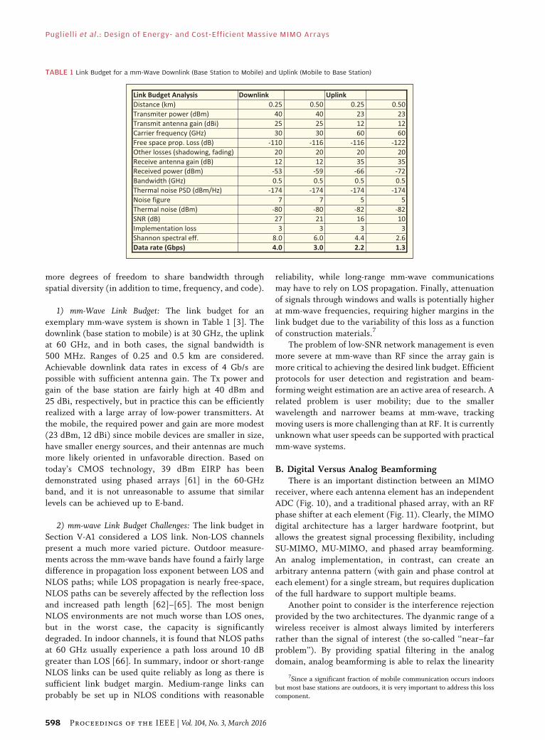
1) mm-Wave Link Budget: The link budget for an
exemplary mm-wave system is shown in Table 1 [3]. The
downlink (base station to mobile) is at 30 GHz, the uplinkat 60 GHz, and in both cases, the signal bandwidth is
500 MHz. Ranges of 0.25 and 0.5 km are considered.
Achievable downlink data rates in excess of 4 Gb/s are
possible with sufficient antenna gain. The Tx power and
gain of the base station are fairly high at 40 dBm and
25 dBi, respectively, but in practice this can be efficiently
realized with a large array of low-power transmitters. At
the mobile, the required power and gain are more modest(23 dBm, 12 dBi) since mobile devices are smaller in size,
have smaller energy sources, and their antennas are much
more likely oriented in unfavorable direction. Based on
today’s CMOS technology, 39 dBm EIRP has been
demonstrated using phased arrays [61] in the 60-GHz
band, and it is not unreasonable to assume that similar
levels can be achieved up to E-band.
2) mm-wave Link Budget Challenges: The link budget in
Section V-A1 considered a LOS link. Non-LOS channels
present a much more varied picture. Outdoor measure-
ments across the mm-wave bands have found a fairly large
difference in propagation loss exponent between LOS and
NLOS paths; while LOS propagation is nearly free-space,
NLOS paths can be severely affected by the reflection loss
and increased path length [62]–[65]. The most benignNLOS environments are not much worse than LOS ones,
but in the worst case, the capacity is significantly
degraded. In indoor channels, it is found that NLOS paths
at 60 GHz usually experience a path loss around 10 dB
greater than LOS [66]. In summary, indoor or short-range
NLOS links can be used quite reliably as long as there is
sufficient link budget margin. Medium-range links can
probably be set up in NLOS conditions with reasonable
reliability, while long-range mm-wave communications
may have to rely on LOS propagation. Finally, attenuation
of signals through windows and walls is potentially higher
at mm-wave frequencies, requiring higher margins in the
link budget due to the variability of this loss as a function
of construction materials.7
The problem of low-SNR network management is even
more severe at mm-wave than RF since the array gain is
more critical to achieving the desired link budget. Efficient
protocols for user detection and registration and beam-
forming weight estimation are an active area of research. A
related problem is user mobility; due to the smaller
wavelength and narrower beams at mm-wave, tracking
moving users is more challenging than at RF. It is currentlyunknown what user speeds can be supported with practical
mm-wave systems.
B. Digital Versus Analog BeamformingThere is an important distinction between an MIMO
receiver, where each antenna element has an independent
ADC (Fig. 10), and a traditional phased array, with an RF
phase shifter at each element (Fig. 11). Clearly, the MIMO
digital architecture has a larger hardware footprint, butallows the greatest signal processing flexibility, including
SU-MIMO, MU-MIMO, and phased array beamforming.
An analog implementation, in contrast, can create an
arbitrary antenna pattern (with gain and phase control at
each element) for a single stream, but requires duplication
of the full hardware to support multiple beams.
Another point to consider is the interference rejection
provided by the two architectures. The dyanmic range of awireless receiver is almost always limited by interferers
rather than the signal of interest (the so-called ‘‘near–far
problem’’). By providing spatial filtering in the analog
domain, analog beamforming is able to relax the linearity
TABLE 1 Link Budget for a mm-Wave Downlink (Base Station to Mobile) and Uplink (Mobile to Base Station)
7Since a significant fraction of mobile communication occurs indoorsbut most base stations are outdoors, it is very important to address this losscomponent.
Puglielli et al. : Design of Energy- and Cost-Efficient Massive MIMO Arrays
598 Proceedings of the IEEE | Vol. 104, No. 3, March 2016
requirements of the receive chain by attenuating out-of-
beam interferers. In contrast, since spatial filtering does
not occur until after digitization, each receiver in the
digital beamforming architecture must handle the full
interferer strength.
1) Baseband Analog Beamforming and Nulling: Given thatRF phase shifters are bulky and lossy, we have proposed
baseband analog beamforming and nulling [67], which is
accomplished by simply taking weighted combinations of
the baseband I and Q waveforms. Current-domain
summation can be implemented with minimal loss
compared to RF combining, and the architecture is well
suited to forming beams across the boundary of multiple
chips, as high bandwidth currents can be routed off-chipand summed in an efficient manner.
On the transmitter side, baseband analog beamforming
and nulling is even more compelling, as the phase shifting
and amplitude scaling can be embedded into the analog
modulation process with little overhead. In fact, due to the
plethora of antennas, we can go one step further and use
the array to not only do beamforming or nulling, but to
form higher order constellations. In [68], we synthesized a16-QAM waveform from an array of 4 I and 4 Q antenna
elements. The antenna elements were partitioned akin to a
segmented DAC, with three of the four elements unary
weighted and a single-element binary weighted with 2-bits
of resolution. This allowed the transmitters to be much
more efficient by utilizing highly nonlinear switching
amplifier topologies (Class E=F2).
2) Hybrid Beamforming: An appealing architecture for
mm-wave bands is a hybrid digital/analog approach where
subarrays of antennas are controlled using analog
beamforming. These subarrays can be used directly to
sectorize the environment (Fig. 12) or can be followed by a
lower-dimensional digital beamformer that is able to
generate more complex beampatterns [69]–[72]. A hybrid
architecture can balance the reduced complexity of analogbeamforming with the greater flexibility of digital
beamforming.
3) Interference Mitigation and Spatial Diversity: As we
have seen, arrays of radios are used to minimize
interference through transmit and receive beamforming,
essentially filtering the signal in the angular domain. The
detrimental impact of multipath propagation is alsominimized since multipath components at most angles of
arrival will be filtered by the receiver beampattern.
Moreover, when a receiver link margin is not noise-
limited, but rather interference-limited, some gain can be
traded off and a beam null can be intentionally inserted
into the pattern in the direction of an interferer (Fig. 13),
in theory completely eliminating the undesired signal. In
Fig. 10. Fully digital MIMO system. Note that spatial filtering does not
occur until the baseband, which means the entire front end is subject to
interference from all directions.
Fig. 11. RF phase-shifting array. Since spatial filtering occurs at the
front end after the phase shifters, the subsequent blocks have relaxed
linearity requirements.
Fig. 12. Hybrid analog/digital array receiver array. Note that a cluster
of streams is routed to a subarray of antennas, each cluster pointing in
a programmable direction through analog beamforming. Digital
pattern shown is for illustrative purposes only; in reality, a generalized
beam will be formed.
Puglielli et al. : Design of Energy- and Cost-Efficient Massive MIMO Arrays
Vol. 104, No. 3, March 2016 | Proceedings of the IEEE 599
practice, beam nulling requires very high precision in the
beam coefficients, and any amplitude error ð��Þ or phasemismatches ð�Þ, arising from quantization noise, phase
noise, and other nonidealities, limits the peak-to-null ratio
to 10 logð�2� þ �2
Þ � 10 logðMÞ [73].
4) True Time Delay Array: As discussed in Section III-A,
when the propagation time across the array aperture is
comparable to the symbol period, wideband beamforming
techniques must be used. In a mm-wave system, this willalmost always involve the use of analog TTD elements,
which is generally bulkier and lossier than a phase shifter.
In many cases, switched transmission lines, or artificial
delay lines, are employed. In [74], an integrated variable
time-delay architecture is proposed, but fundamentally the
size of the realizable array is limited by the achievable
maximum delay. The time-delay element can be embedded
into the amplifiers in a chain, thereby absorbing devicecapacitance into the structure as well [75].
C. mm-Wave LO DistributionSynchronization specifications for a large array are
presented in Section IV-C, leading to an architecture
where a common low-frequency reference is distributed
across the array, and the LO and sampling clocks are
generated locally for a single element or a small group of
elements. One can think of this as taking a single PLL,
segmenting it, and placing the segments close to antennas
they serve. Since the phase noise of an oscillator is
inversely proportional to its power dissipation, byexploiting the phase noise averaging, different amounts
of PLL segmentation will, to first order, consume the
same total power for a given system phase noise
specification. However, due to factors such as PLL
overhead power, routing loss, and VCO efficiency, the
amount of segmentation will greatly affect the overall
system power. The following sections will discuss these
tradeoffs and how they influence the overall LOdistribution architecture.
1) LO Routing: When planning the routing of a large
array, one important consideration is the phase/delay
shifting capability required of each element. Since even
phased arrays can naturally calibrate for LO routing skew
(Section IV-C2), signal distribution to a large number of
elements will not necessarily require skew matchingschemes such as H-trees. Therefore, the total route length
can in principle grow linearly instead of exponentially.
Another important consideration is the ratio between
LO power consumption required to meet the phase noise
specification and the LO power that needs to be delivered
to the load. If these are similar, then any routing losses will
dissipate significant amounts of power. If instead the load
requires much higher power levels than the source, the LOcan be routed with little efficiency loss and gain elements
can be used at the load to deliver the required power. In
practice, due to the limited achievable transmission line
impedances, it will be necessary to distribute gain elements
along the LO distribution network. This reduces the
efficiency, but allows for more realistic line impedances.
2) VCO Efficiency: As mentioned earlier, the phase noiseof an oscillator is inversely proportional to the power
dissipated. The VCO figure of merit (FOM) is a useful
metric to compare multiple VCOs at different phase noise
levels
FOM ¼ 10 logLfDfg PDC
1 mW
f0Df
� �2
0@
1A: (17)
Here, LfDfg is the phase noise at offset frequency Df from
the resonance frequency f0, and PDC is the oscillator’spower consumption. It has been discussed in [76] that for
any LC oscillator with efficiency �, noise factor F, and tank
quality factor Q, the FOM can be described in the
following form:
FOM ¼ 10 logkTF
2�Q210�3
� �(18)
and that for an efficiency of 100% and a noise factor of
ð1þ �Þ, the maximum achievable FOM is
FOMopt ¼ �174:6� 20 log Q: (19)
In [76], a VCO within 1.5 dB of this optimal FOM was
demonstrated at RF. While efficiencies will typically be
Fig. 13. Receiver that performs beamforming and nulling to maximize
SNDR.
Puglielli et al. : Design of Energy- and Cost-Efficient Massive MIMO Arrays
600 Proceedings of the IEEE | Vol. 104, No. 3, March 2016
lower at mm-wave, for a given VCO topology, the FOM islargely dependent on the tank Q.
When the system’s PLL is divided into NPLL segments,
the power of each VCO should decrease by NPLL, and its
noise should increase by the same factor for constant
FOM. However, to reduce the power, the tank impedance
will also need to be increased by NPLL. Achievable values
of Q may vary dramatically for different tank impedances,
which will change the FOM and cause the power–noisetradeoff to deviate from the ideal relationship. For
instance, very large values of inductance may lead to
operation too close to the self-resonant frequency (SRF),
and very small values of inductance may require small
wires and be highly resistive. When deciding on the level
of PLL segmentation, the achievable tank impedances will
affect the range of feasible options and may significantly
change the optimum. At mm-wave frequencies, evenrelatively small inductances will yield large tank impe-
dances with good Q, which may drive mm-wave systems to
higher levels of optimum segmentation than RF systems.
3) PLL Bandwidth: In most situations, a low-frequencycrystal reference will be required to achieve the specified
frequency error and low-frequency phase noise. The available
frequencies of crystals range from the low-MHz range up to a
few hundred MHz, with a phase noise floor on the order of
�150 dBc/Hz. In RF systems, frequency multiplication will
lead to in band reference noise on the order of�115 dBc/Hz,
which is well within tolerable levels for high-order constella-
tions, even with relatively low carrier recovery (CR)bandwidths. At mm-wave, since the reference frequency is
multiplied by around 1000�, the in-band phase noise of the
PLL is limited to approximately �90 dBc/Hz. This will
potentially be a significant contributor to the overall
integrated phase error and limit the constellation order,
unless aggressive CR bandwidths are pursued.
Traditionally, for a given reference noise and oscillator
noise level, the PLL bandwidth is selected to achieve thelowest amount of integrated phase noise at the PLL output.
In Section IV-C3, it was shown that the PLL bandwidth
should be set close to the CR bandwidth. Combining these
two requirements, the optimum value of the PLL
bandwidth will be a function of both the CR bandwidth
and the relative noise levels between the reference and
oscillator as in a conventional PLL design. The choice of
the common reference frequency will also depend uponthe CR bandwidth and the optimal PLL bandwidth.
D. Antennas and Packaging Challenges at mm-WaveTwo key challenges in realizing a complete mm-wave
phased array system are the IC packaging and antenna design.
density flip-chip packaging is critical to meet these challenges.
1) Overview: Unlike at lower frequencies, where
antennas and packaging may be decoupled in practice, at
mm-wave they are typically co-optimized to minimizerouting losses and control parasitic coupling. The result is
a combined chip-antenna module, with only low-frequency
electrical interfaces to the outside world, other than the
transmitted and received electromagnetic radiation from
the antennas themselves. Modules are typically realized as
a ball-grid array (BGA) package built on a low-loss
substrate, such as low-temperature co-fired ceramic
(LTCC) or high-performance laminates such as Rogers4003C [77] or Taconic TLY-05 [78]. An example diagram
of a mm-wave BGA module previously characterized at the
BWRC is shown in Fig. 14.
The inductances and capacitances associated with
conventional bondwire-based packaging become increas-
ingly problematic at mm-wave frequencies, which lead to
the use of flip-chip packaging techniques. Since flip-chip
also allows for area-array IO pads (in the interior of thechip, as well as around the perimeter), it also helps to
reduce routing complexity in phased arrays with many
elements. Antenna elements can be directly above the
corresponding transceiver element on the RFIC without
having to increase element-to-element spacing, or resort-
ing to convoluted phase-matched routing lines.
BGA packages also tend to have many metallization
layers, each satisfying different requirements. RF feedlinesand antennas can be on their own layers to minimize
coupling to the rest of the circuits. Thicker power planes
on separate layers minimize ohmic losses in the supply
networks. IF outputs and digital control signals may be on
yet another routing layer. The result is a complex,
multilayer stack that can have as little as 4 or as many as
12 or more routing layers [79], [80]. Dielectric materials
and thicknesses must be carefully chosen to optimizeantenna performance.
2) Antenna Design: For the base station, particularly in a
sectorized system, higher-gain antennas such as horn
arrays can be employed to increase gain while trading off
beam-steering range. In mobile devices, the vast majority
of mm-wave antenna modules make use of microstrip
patch antennas, which is compatibile with planar PCB and
Fig. 14. mm-wave antenna module with BGA footprint, implementing
a quadrature spatial combining transmitter [68], [79]. To reduce its
impact on the radiation pattern, the silicon RFIC is attached on the
opposite side of the package as the antennas.
Puglielli et al. : Design of Energy- and Cost-Efficient Massive MIMO Arrays
Vol. 104, No. 3, March 2016 | Proceedings of the IEEE 601
packaging technologies. Additionally, the ground plane ofthe patch helps isolate signals on lower layers from the
antenna and feedlines. Patch antennas are typically fairly
narrowband unless implemented on thick and/or low
dielectric constant substrates [81]. Substrates cannot be
made arbitrarily thick without losses from surface waves,
so to further increase bandwidth, aperture, or proximity,
coupling is used [82].
To reduce unwanted radiation and coupling fromantenna feedlines, RF routing layers have a completely
opposite set of criteria from the substrate. Thin, high
dielectric constant layers are desirable in this case. This
mismatch in substrate requirements is one of the factors
leading to increased package complexity, as separate RF
routing and antenna layers are needed.
3) Large-Scale Array Integration: Developing a large-scale phased array that integrates many die or modules
presents additional challenges. To avoid grating lobes in
the radiation pattern, antenna elements should be spaced
at �=2. This requires adjacent modules to be closely
abutted, creating additional problems in routing signals
from the BGA pads. Conversely, including many die in a
single package increases the area and routing complexity
of the package, driving up its cost. Some success hasbeen demonstrated in scalable array archictures using
conventional BGA techniques but with an aggressive
layer count [80] or more experimental wafer-level
packaging [83].
VI. CONCLUSION
In this paper we have reviewed the state of the art in large
antenna arrays for massive MIMO and presented keyalgorithms, architectures, and design techniques to build
these systems in a cost- and energy-efficient manner at both
RF and mm-wave frequencies. Arrays and their associated
spatial signal processing techniques are a key technology
for interference mitigation at both the base station as well
as certain user devices. Cost- and energy-efficient arrays are
therefore a central element in our vision of an xG network
where a wide range of devicesVfrom energy-starvedsensors to high-power personal computersVcommunicate
with the network over directional, high-bandwidth links
even in very dense environments. Additionally, deploying
very highly directional xG hubs in a wireless mesh network
can significantly speed up and lower the cost of network
infrastructure deployment while making the network itself
more robust. Though there are many open research
questions in both implementation and network manage-ment, large arrays look to be a very promising technology. h
Acknowledgment
Special thanks to the DARPA TEAM program (60 GHz),
the DARPA Wafer Scale Radio Seedling [84], the FCRP-
C2S2 Program, and continuing programs such as the NSF
THz Chip-to-Chip (ECCS-1201755), NSF EARS, and theDARPA RF-FPGA and Arrays at Commercial Timescale
(ACT) programs.
REF ERENCE S
[1] A. M. Niknejad et al., ‘‘The xG Vision: Makingthe Internet truly wireless.’’ [Online].Available: http://files-eu.clickdimensions.com/ericssoncom-anlg4/documents/xg_vision_5g_public_.pdf
[2] ITU ‘‘Framework and overall objectives of thefuture development of IMT for 2020 andbeyond,’’ presented at the 18th Meeting ofITU Working Party 5D, Feb. 2014.
[3] C. J. Zhang, ‘‘Realizing massive MIMO inLTE-Advanced and 5G,’’ presented at theBrooklyn 5G Summit, Apr. 2015.
[4] B. V. Veen and K. Buckley, ‘‘Beamforming: Aversatile approach to spatial filtering,’’ IEEEASSP Mag., vol. 5, no. 2, pp. 4–24, Apr. 1988.
[5] Increasing capacity in wireless broadcastsystems using Distributed Transmission/Directional Reception (DTDR), byA. J. Paulraj and T. Kailath, U.S. 1994,Patent 5 345 599. [Online]. Available: http://www.google.com/patents/US5345599
[6] S. Talwar, M. Viberg, and A. J. Paulraj, ‘‘Blindestimation of multiple co-channel digitalsignals using an antenna array,’’ IEEE SignalProcess. Lett., vol. 1, no. 2, pp. 29–31,Feb. 1994.
[7] G. J. Foschini and M. J. Gans., ‘‘On limits ofwireless communications in a fadingenvironment when using multiple antennas,’’Wireless Pers. Commun., vol. 6, pp. 311–335,Mar. 1998.
[8] I. E. Telatar, ‘‘Capacity of multi-antennaGaussian channels,’’ Eur. Trans. Telecommun.,vol. 10, no. 6, pp. 585–595, 1999.
[9] P. Wolniansky, G. J. Foschini, G. D. Golden,and R. Valenzuela, ‘‘V-BLAST: Anarchitecture for realizing very high data ratesover the rich-scattering wireless channel,’’ inProc. URSI Int. Symp. Signals, Syst. Electron.,1998, pp. 295–300.
[10] Wireless LAN Media Access Control (MAC)and Physical Layer (PHY) Specifications,IEEE Std. 802.11n-2009, 2009.
[12] TDM-based fixed wireless loop system, byD. Avidor, S. Kasturia, T. Sizer, R. Valenzuela,and G. A. Wright, U.S. Patent 6 961 325,2005. [Online]. Available: http://www.google.com/patents/US6961325
[14] T. L. Marzetta, ‘‘Noncooperative cellularwireless with unlimited numbers of basestation antennas,’’ IEEE Trans. WirelessCommun., vol. 9, no. 11, pp. 3590–3600,Nov. 2010.
[15] X. Gao, F. Tufvesson, O. Edfors, and F. Rusek,‘‘Measured propagation characteristics forvery-large MIMO at 2.6 GHz,’’ in Conf. Rec.46th Asilomar Conf. Signals, Syst. Comput.,Nov. 2012, pp. 295–299.
[16] J. Hoydis, S. ten Brink, and M. Debbah,‘‘Comparison of linear precoding schemes fordownlink massive MIMO,’’ in Proc. IEE ICC,Jun. 2012, pp. 2135–2139.
[17] J. Hoydis, S. ten Brink, and M. Debbah,‘‘Massive MIMO in the UL/DL of cellularnetworks: How many antennas do we need?’’IEEE J. Sel. Areas Commun., vol. 31, no. 2,pp. 160–171, Feb. 2013.
[18] Z. Pi and F. Khan, ‘‘A millimeter-wavemassive MIMO system for next generationmobile broadband,’’ in Conf. Rec. 46th AsilomarConf. Signals, Syst. Comput., Nov. 2012,pp. 693–698.
[19] T. S. Rappaport et al., ‘‘Millimeter wavemobile communications for 5G cellular: Itwill work!’’ IEEE Access, vol. 1, pp. 335–349,2013.
[21] H. Suzuki et al., ‘‘Highly spectrally efficientNgara rural wireless broadband accessdemonstrator,’’ in Proc. Int. Symp. Commun.Inf. Technol. (ISCIT), Oct. 2012, pp. 914–919.
[22] H. Suzuki et al., ‘‘Large-scale multiple antennafixed wireless systems for rural areas,’’ inProc. 23rd IEEE Int. Symp. Pers. Indoor MobileRadio Commun. (PIMRC), Sep. 2012,pp. 1600–1605.
[23] X. Huang, Y. J. Guo, A. Zhang, andV. Dyadyuk, ‘‘A multi-gigabit microwavebackhaul,’’ IEEE Commun. Mag., vol. 50, no. 3,pp. 122–129, Mar. 2012.
[24] H. V. Balan et al., ‘‘USC SDR, an easy-to-program, high data rate, real time softwareradio platform,’’ in Proc. ACM SIGCOMM 2nd
Puglielli et al. : Design of Energy- and Cost-Efficient Massive MIMO Arrays
602 Proceedings of the IEEE | Vol. 104, No. 3, March 2016
Workshop Softw. Radio Implement. Forum,Aug. 2013, pp. 25–30.
[25] C. Shepard et al., ‘‘Argos: Practicalmany-antenna base stations,’’ in Proc. 18thInt. Conf. Mobile Comput. Netw. (MobiCom),Aug. 2012, pp. 53–64.
[26] C. Shepard, H. Yu, and L. Zhong, ‘‘ArgosV2: Aflexible many-antenna research platform,’’ inProc. 19th Int. Conf. Mobile Comput. Netw.(MobiCom), Oct. 2013, pp. 163–166.
[27] H. Yang and T. L. Marzetta, ‘‘Performance ofconjugate and zero-forcing beamforming inlarge-scale antenna systems,’’ IEEE J. Sel.Areas Commun., vol. 31, no. 2, pp. 172–179,Feb. 2013.
[28] J. Vieira et al., ‘‘A flexible 100-antenna testbedfor massive MIMO,’’ in Proc. IEEEGLOBECOM 2014 Workshops, Dec. 2014,pp. 287–293.
[29] X. Gao, O. Edfors, F. Rusek, and F. Tufvesson,‘‘Massive MIMO performance evaluationbased on measured propagation data,’’ IEEETrans. Wireless Commun., vol. 14, no. 7,pp. 3899–3911, Jul. 2015.
[32] E. Larsson, O. Edfors, F. Tufvesson, andT. L. Marzetta, ‘‘Massive MIMO fornext generation wireless systems,’’ IEEECommun. Mag., vol. 52, no. 2, pp. 186–195,Feb. 2014.
[33] H. Huh, G. Caire, H. C. Papadopoulos, andS. A. Ramprashad, ‘‘Achieving ‘massiveMIMO’ spectral efficiency with a not-so-largenumber of antennas,’’ IEEE Trans. WirelessCommun., vol. 11, no. 9, pp. 3226–3239,Sep. 2012.
[34] Y. Kim et al., ‘‘Evolution beyond LTE-advanced with full dimension MIMO,’’ inProc. 2013 IEEE Int. Conf. Commun. (ICC)Workshops, 2013, pp. 111–115.
[35] Y.-H. Nam et al., ‘‘Full-dimension MIMO(FD-MIMO) for next generation cellulartechnology,’’ IEEE Commun. Mag., vol. 51,no. 6, pp. 172–179, Jun. 2013.
[36] Y. Kim et al., ‘‘Full dimension MIMO(FD-MIMO): The next evolution of MIMO inLTE systems,’’ IEEE Wireless Commun. Mag.,vol. 21, no. 2, pp. 92–100, Jun. 2014.
[37] B. Lee, J. Choi, J.-Y. Seol, D. J. Love, andB. Shim, ‘‘Antenna grouping based feedbackreduction for FDD-based massive MIMOsystems,’’ in Proc. IEEE Int. Conf. Commun.(ICC), Jun. 2014, pp. 4477–4482.
[38] Z. Jiang, A. F. Molisch, G. Caire, and Z. Niu,‘‘Achievable rates of FDD massive MIMOsystems with spatial channel correlation,’’IEEE Trans. Wireless Commun., vol. 14, no. 5,pp. 2868–2882, May 2015.
[39] F. Rusek et al., ‘‘Scaling up MIMO:Opportunities and challenges with very largearrays,’’ IEEE Signal Process. Mag., vol. 30,no. 1, pp. 40–60, Jan. 2013.
[40] L. Lu, G. Y. Li, A. L. Swindlehurst,A. Ashikhmin, and R. Zhang, ‘‘An overview ofmassive MIMO: Benefits and challenges,’’IEEE J. Sel. Topics Signal Process., vol. 8, no. 5,pp. 742–758, Oct. 2014.
[41] H. Q. Ngo, E. G. Larsson, and T. L. Marzetta,‘‘Massive MU-MIMO downlink TDD systemswith linear precoding and downlink pilots,’’ inProc. 51st Allerton Conf. Commun., Control,Comput., Oct. 2013, pp. 293–298.
[42] E. Luther, ‘‘5G massive MIMO testbed: Fromtheory to reality,’’ National Instruments,Tech. Rep. [Online]. Available: http://www.ni.com/white-paper/52382/en/
[43] M. Brown and M. Turgeon, ‘‘TitanMIMO: A100� 100 massive MIMO testbed based onxTCA,’’ Nutaq Corp., Tech. Rep. [Online].Available: http://www.nutaq.com
[44] A. Puglielli et al., ‘‘A scalable massive MIMOarray architecture based on commonmodules,’’ in Proc. 2015 IEEE Int. Conf.Commun. (ICC) Workshops, Jun. 2015,pp. 1284–1289.
[45] L. Kong, ‘‘Energy-efficient 60 GHzphased-array design for multi-Gb/scommunication systems,’’ Ph.D. dissertation,EECS Department, University of California,Berkeley, CA, USA, Dec. 2014.
[46] H. Q. Ngo, E. G. Larsson, and T. L. Marzetta,‘‘Energy and spectral efficiency of very largemultiuser MIMO systems,’’ IEEE Trans.Commun., vol. 61, no. 4, pp. 1436–1449,Apr. 2013.
[47] K. F. Warnick, M. Ivashina, R. Maaskant, andB. Woestenburg, ‘‘Unified definitions ofefficiencies and system noise temperaturefor receiving antenna arrays,’’ IEEE Trans.Antennas Propag., vol. 58, no. 3, pp. 2121–2125,Mar. 2010.
[48] K. F. Warnick and B. Jeffs, ‘‘Efficiencies andsystem temperature for a beamforming array,’’IEEE Antennas Wireless Propag. Lett., vol. 7,pp. 565–568, 2008.
[49] M. Ivashina, R. Maaskant, andB. Woestenburg, ‘‘Equivalent systemrepresentation to model the beam sensitivityof receiving antenna arrays,’’ IEEE AntennasWireless Propag. Lett., vol. 7, pp. 733–737,2008.
[50] K. Lauritzen, ‘‘Correlation of signals, noise,harmonics in parallel analog-to-digitalconverter arrays,’’ Ph.D. dissertation, ECEDepartment, University of Maryland, CollegePark, MD, USA, Dec. 2009. [Online].Available: http://hdl.handle.net/1903/9608.
[51] S. Wu and Y. Bar-Ness, ‘‘OFDM systems inthe presence of phase noise: Consequencesand solutions,’’ IEEE Trans. Commun., vol. 52,no. 11, pp. 1988–1996, Nov. 2004.
[52] S. Wu and Y. Bar-Ness, ‘‘A phase noisesuppression algorithm for OFDM-basedWLANs,’’ IEEE Commun. Lett., vol. 6, no. 12,pp. 535–537, Dec. 2002.
[53] P. Robertson and S. Kaiser, ‘‘Analysis of theeffects of phase noise in orthogonal frequencydivision multiplex (OFDM) systems,’’ in Proc.IEEE Int. Conf. Commun. (ICC), Jun. 1995,pp. 1652–1657.
[54] D. Petrovic, W. Rave, and G. Fettweis,‘‘Effects of phase noise on OFDM systemswith and without PLL: Characterization andcompensation,’’ IEEE Trans. Commun., vol. 55,no. 8, pp. 1607–1616, Aug. 2007.
[55] A. Puglielli et al., ‘‘Phase Noise Scaling andTracking in OFDM Multi-user BeamformingArrays,’’ in review.
[56] T. Hohne and V. Ranki, ‘‘Phase noise inbeamforming,’’ IEEE Trans. Wireless Commun.,vol. 9, no. 12, pp. 3682–3689, Dec. 2010.
[57] A. Pitarokoilis, S. K. Mohammed, andE. G. Larsson, ‘‘Uplink performance oftime-reversal MRC in massive MIMO systemssubject to phase noise,’’ IEEE Trans. WirelessCommun., vol. 14, no. 2, pp. 711–723,Feb. 2015.
[58] Federal Communications Commission, Officeof Engineering and Technology, NewTechnology Development DivisionMillimeterwave propagation: Spectrum managementimplications, Tech. Rep. Bulletin Number 70,Jul. 1997.
[59] C. Waldschmitt, C. Kuhnert, S. Schulteis, andW. Wiesbeck, ‘‘Compact MIMO-arrays
based on polarisation-diversity,’’ in Proc. IEEEInt. Symp. Antennas Propag., Jun. 2003,pp. 499–502.
[60] R. Salman, I. Willms, L. Reichardt, T. Zwick,and W. Wiesbeck, ‘‘On polarization diversitygain in short range UWB-radar object imaging,’’in Proc. IEEE Int. Conf. Ultra-Wideband(ICUWB), Sep. 2012, pp. 402–406.
[61] A. Valdes-Garcia et al., ‘‘Single-element andphased-array transceiver chipsets for 60 GHzGb/s communications,’’ IEEE Commun. Mag.,vol. 49, no. 4, pp. 120–131, Apr. 2011.
[62] N. Shuai, G. R. MacCartney, S. Shu, andT. S. Rappaport, ‘‘72 GHz millimeter waveindoor measurements for wireless andbackhaul communications,’’ in Proc. 24th IEEEInt. Symp. Pers. Indoor Mobile Radio Commun.(PIMRC), Sep. 2013, pp. 2429–2433.
[63] M. Samimi et al., ‘‘28 GHz angle of arrivaland angle of departure analysis for outdoorcellular communications using steerablebeam antennas in New York City,’’ in Proc.77th IEEE Veh. Technol. Conf. (VTC Spring),Jun. 2013, pp. 1–6.
[64] T. S. Rappaport et al., ‘‘Broadbandmillimeter-wave propagation measurementsand models using adaptive-beam antennasfor outdoor urban cellular communications,’’IEEE Trans. Antennas Propag., vol. 61, no. 4,pp. 1850–1859, Apr. 2012.
[65] S. Rangan, T. S. Rappaport, and E. Erkip,‘‘Millimeter-wave cellular wireless networks:Potentials and challenges,’’ Proc. IEEE,vol. 102, no. 3, pp. 366–385, Mar. 2014.
[66] X. Hao, V. Kukshya, and T. Rappaport,‘‘Spatial and temporal characteristics of60 GHz indoor channels,’’ IEEE J. Sel. AreasCommun., vol. 20, no. 3, pp. 620–630,Apr. 2002.
[67] M. Tabesh et al., ‘‘A 65 nm CMOS 4-elementsub-34 mW/element 60 GHz phased-arraytransceiver,’’ IEEE J. Solid-State Circuits,vol. 46, no. 12, pp. 3018–3032, Dec. 2011.
[68] J. Chen et al., ‘‘A digitally modulatedmm-wave cartesian beamforming transmitterwith quadrature spatial combining,’’ in Int.Solid-State Circuits Conf. (ISCC) Dig. Tech.Papers, Feb. 2013, pp. 232–233.
[69] A. Alkhateeb, O. E. Ayach, G. Leus, andR. W. Heath, ‘‘Channel estimation and hybridprecoding for millimeter wave cellularsystems,’’ IEEE J. Sel. Topics Signal Process.,vol. 8, no. 5, pp. 831–846, Oct. 2014.
[70] A. Alkhateeb, J. Mo, N. G. Prelcic, andR. W. Heath, ‘‘MIMO precoding andcombining solutions for millimeter-wavesystems,’’ IEEE Commun. Mag., vol. 52, no. 12,pp. 122–131, Dec. 2014.
[71] W. Roh et al., ‘‘Millimeter-wave beamformingas an enabling technology for 5G cellularcommunications: Theoretical feasibility andprototype results,’’ IEEE Commun. Mag.,vol. 52, no. 2, pp. 106–113, Feb. 2014.
[72] O. E. Ayach, S. Rajagopal, S. Abu-Surra, Z. Pi,and R. W. Heath, ‘‘Spatially sparse precodingin millimeter wave MIMO systems,’’ IEEETrans. Wireless Commun., vol. 13, no. 3,pp. 1499–1513, Mar. 2014.
[73] O. Bakr, ‘‘A scalable and cost effectivearchitecture for high gain beamformingantennas,’’ U.C. Berkeley, Tech. Rep.No. UCB/EECS-2010-178, Dec. 2010.
[74] E. Adabi and A. M. Niknejad, ‘‘Broadbandvariable passive delay elements based on aninductance multiplication technique,’’ in Proc.IEEE Radio Freq. Integrated Circuits Symp.,Jun. 2008, pp. 445–448.
[75] E. A. Firouzjaei, ‘‘mm-wave phase shiftersand switches,’’ Ph.D. dissertation, EECS
Puglielli et al. : Design of Energy- and Cost-Efficient Massive MIMO Arrays
Vol. 104, No. 3, March 2016 | Proceedings of the IEEE 603
Department, University of California,Berkeley, CA, USA, Dec. 2010. [Online].Available: http://www.eecs.berkeley.edu/Pubs/TechRpts/2010/EECS-2010-163.html.
[76] T. L. Marzetta, ‘‘Noncooperative cellularwireless with unlimited numbers of basestation antennas,’’ IEEE Trans. WirelessCommun., vol. 9, no. 11, pp. 1436–1449,Nov. 2010.
[78] Taconic Advanced Dielectric Division, (2012),TLY family of low-loss laminates. [Online].Available: http://www.taconic-add.com/pdf/tly.pdf
[79] D. Titz et al., ‘‘Antenna-array topologies formm-wave beamforming transmitter withquadrature spatial combining,’’ in Proc.IEEE-APS Top. Conf. Antennas Propag. WirelessCommun. (APWC), Aug. 2014, pp. 399–402.
[80] X. Gu et al., ‘‘A compact 4-chip package with64 embedded dual-polarization antennas forW band phased-array transceivers,’’ in Proc.64th IEEE Electron. Compon. Technol. Conf.(ECTC), May 2014, pp. 1272–1277.
[81] R. Waterhouse, Microstrip Patch Antennas:A Designer’s Guide. New York, NY, USA:Springer-Verlag, 2003.
[82] D. G. Kam, D. Liu, A. Natarajan, S. Reynolds,and B. Floyd, ‘‘Organic packages withembedded phased-array antennas for 60 GHzwireless chipsets,’’ IEEE Trans. Compon.
[83] W. Shin, B.-H. Ku, O. Inac, Y.-C. Ou, andG. Rebeiz, ‘‘A 108 GHz 4� 4 wafer-scalephased array transmitter with high-efficiencyon-chip antennas,’’ IEEE J. Solid-State Circuits,vol. 48, no. 9, pp. 2041–2055, Sep. 2013.
[84] A. M. Niknejad, E. Alon, B. Nikolic, andJ. Rabaey, ‘‘Wafer scale distributed radio,’’Air Force Research Laboratory, Tech. Rep.ARFL-RY-WP-TR-2009-1172. [Online].Available: http://www.dtic.mil/cgi-bin/GetTRDoc?Location=U2&doc=GetTRDoc.pdf&AD=ADA504367
ABOUT THE AUT HORS
Antonio Puglielli (Student Member, IEEE) re-
ceived the B.S. degree in applied math, engineer-
ing, and physics (AMEP) from the University of
Wisconsin-Madison, Madison, WI, USA, in 2013,
and is currently pursuing the Ph.D. degree in
electrical engineering at the University of
California, Berkeley, CA, USA.
He has held internship positions with National
Instruments, Qualcomm, and Intel. His current
research interests are in the field of analog and
digital signal processing algorithms, circuits, and systems.
Andrew Townley (Student Member, IEEE) re-
ceived the B.S. and M.S. degrees in electrical
engineering from the University of Pennsylvania,
Philadelphia, PA, USA, in 2011, and is currently
pursuing the Ph.D. degree in electrical engineering
at the University of California, Berkeley, CA, USA.
During his Ph.D. career, he has held internship
positions with Nokia, Analog Devices, and Google.
His current research interests are in millimeter-
wave circuit design and packaging for sensing and
communication applications.
Greg LaCaille (Student Member, IEEE) received
the B.S. and M.S. degree in electrical engineering
from California Polytechnic State University,
San Luis Obispo, CA, USA, in 2010, and is currently
pursuing the Ph.D. degree in electrical engineering
at the University of California, Berkeley, CA, USA.
Between 2010 and 2012, he worked with the
Lawrence Livermore National Laboratory,
Livermore, CA, USA, designing X-ray diagnostics
for experiments at the National Ignition Facility.
He has interned with Altera, Apple, and Intel working on integrated
circuit frequency synthesizers. He is an active member of the Berkeley
Wireless Research Center (BWRC). His research interests are in energy-
efficient frequency synthesizers, integrated circuit design for RF and
millimeter-wave phased arrays, and design automation of analog/RF
integrated circuits.
Vladimir Milovanovic received the Dipl.-Ing.
degree in electrical engineering from the Univer-
sity of Belgrade, Belgrade, Serbia, in 2005, and the
Ph.D. degree from Delft University of Technology,
Delft, The Netherlands, in 2010.
Since the beginning of 2014, he has been
working as a Postdoctoral Scholar with the
University of California, Berkeley, CA, USA, under
the guidance of Prof. Borivoje Nikolic. During the
studies, he was on internships with the TechnionV
Israel Institute of Technology, Haifa, Israel, in summer 2004 and the
Technical University of Madrid, Madrid, Spain, in spring 2005. Before
joining Berkeley’s Department of Electrical Engineering and Computer
Sciences, from 2011 he was with Vienna University of Technology, Vienna,
Austria, as a Postdoctoral Research Fellow.
His research interests include design, modeling, and optimization of
CMOS/BiCMOS analog, mixed-signal, and digital integrated circuits,
devices, and systems, as well as development and implementation
of energy-efficient communication, control, and signal processing
algorithms.
Pengpeng Lu received the Bachelor of Science
degree from Peking University, Beijing, China, in
2012, and the M.S. degree from the University of
California, Berkeley, CA, USA, in 2015, and is
currently pursuing the Ph.D. degree in electrical
engineering and computer science at the Univer-
sity of California, Berkeley.
From May to December 2014, she was an Intern
with Marvell, Inc., Santa Clara, CA, USA, where she
was involved with design and simulation of
digitally controlled ring oscillators for wireless applications. Her research
interests are mixed-signal circuits and design of energy-efficient RF
front-end circuits.
Konstantin Trotskovsky received the B.S. and
M.S. degrees in electrical engineering from the
TechnionVIsrael Institute of Technology, Haifa,
Israel, in 2004 and 2010, respectively, and is
currently pursuing the Ph.D. degree at the
University of California, Berkeley, CA, USA.
From 2004 to 2013, he was with the Israel
Defense Forces (IDF) R&D unit, working on various
analog and RF projects. His research focuses on RF
receivers design for large antenna arrays.
Puglielli et al. : Design of Energy- and Cost-Efficient Massive MIMO Arrays
604 Proceedings of the IEEE | Vol. 104, No. 3, March 2016
Amy Whitcombe received the B.S. degree in
electrical and computer engineering from Olin
College, Needham, MA, USA, in 2013, and is
currently pursuing the Ph.D. degree in electrical
engineering at the University of California,
Berkeley, CA, USA.
Her research interests includedeeply scaled
CMOS technology variability and analog-to-digital
converters for energy-efficient wireless receivers.
Nathan Narevsky (Student Member, IEEE) re-
ceived the B.S. degree in electrical engineering
and computer science from the University of
California, Berkeley, CA, USA, in 2012, and is
currently pursuing the Ph.D. degree in electrical
engineering at the Berkeley Wireless Research
Center.
In 2012, he was an intern with Intel working on
integrated voltage regulators for next-generation
microprocessor dynamic voltage and frequency
scaling. In 2015, he was an intern with Intel Labs working on mixed-signal
equalizers for next-generation millimeter-wave communication systems.
His research interests include energy-efficient analog and mixed-signal
circuit and system design for various applications, including array radio
systems and biomedical devices.
Gregory Wright received the bachelor’s degree in
physics from Harvard University, Cambridge, MA,
USA, the M.A. degree in mathematics from
Cambridge University, Cambridge, U.K., and the
Ph.D. degree in physics from Princeton University,
Princeton, NJ, USA.
He did his postdoctoral studies with Bell Labs
in millimeter-wave astronomy and was a co-
investigator on the Antarctic Submillimeter Tele-
scope and Remote Observatory (AST/RO), the first
permanent astronomical observatory at the South Pole. He was a
Researcher with Bell Labs from 1994 until 2001, after which he co-
founded startups in network performance measurement and RFID
systems. He joined Alcatel-Lucent Bell Labs, Holmdel, NJ, USA, in 2010
as a member of wireless communication research, where he has worked
on new approaches for energy-efficient radios.
Thomas Courtade (Member, IEEE) received the
B.Sc. degree (summa cum laude) in electrical
engineering from Michigan Technological Univer-
sity, Houghton, MI, USA, in 2007, and the M.S. and
Ph.D. degrees from the University of California,
Los Angeles (UCLA), CA, USA, in 2008 and 2012,
respectively.
He is an Assistant Professor with the Depart-
ment of Electrical Engineering and Computer
Sciences, University of California, Berkeley, CA,
USA. Prior to joining UC Berkeley in 2014, he was a Postdoctoral Fellow
supported by the NSF Center for Science of Information.
Dr. Courtade’s honors include a Distinguished Ph.D. Dissertation
Award and an Excellence in Teaching Award from the UCLA Department
of Electrical Engineering, and a Jack Keil Wolf Student Paper Award for
the 2012 International Symposium on Information Theory.
Elad Alon received the B.S., M.S., and Ph.D.
degrees in electrical engineering from Stanford
University, Stanford, CA, USA, in 2001, 2002, and
2006, respectively. In 2007, he joined the Univer-
sity of California, Berkeley, CA, USA, where he is
now an Associate Professor of electrical engineer-
ing and computer sciences as well as a co-director
of the Berkeley Wireless Research Center (BWRC).
He has held advisory, consulting, or visiting
positions with Lion Semiconductor, Cadence,
Xilinx, Wilocity, Oracle, Intel, AMD, Rambus, Hewlett Packard, and IBM
Research, where he worked on digital, analog, and mixed-signal
integrated circuits for computing, test and measurement, power
management, and high-speed communications. His research focuses on
energy-efficient integrated systems, including the circuit, device, com-
munications, and optimization techniques used to design them.
Dr. Alon received the IBM Faculty Award in 2008, the 2009 Hellman
Family Faculty Fund Award, as well as the 2010 UC Berkeley Electrical
Engineering Outstanding Teaching Award, and has coauthored papers
that received the 2010 ISSCC Jack Raper Award for Outstanding
Technology Directions Paper, the 2011 Symposium on VLSI Circuits Best
Student Paper Award, and the 2012 as well as the 2013 Custom Integrated
Circuits Conference Best Student Paper Awards.
Borivoje Nikolic (Senior Member, IEEE) received
the Dipl.Ing. and M.Sc. degrees in electrical
engineering from the University of Belgrade,
Belgrade, Serbia, in 1992 and 1994, respectively,
and the Ph.D. degree from the University of
California, Davis, CA, USA, in 1999.
In 1999, he joined the Department of Electrical
Engineering and Computer Sciences, University of
California, Berkeley, CA, USA, where he is now a
National Semiconductor Distinguished Professor
of Engineering. His research activities include digital, analog, and RF
integrated circuit design and VLSI implementation of communications
and signal processing systems. He is coauthor of the book Digital
Integrated Circuits: A Design Perspective (2nd ed., Prentice-Hall, 2003).
Dr. Nikolic received the NSF CAREER Award in 2003, the College of
Engineering Best Doctoral Dissertation Prize and Anil K. Jain Prize for the
Best Doctoral Dissertation in Electrical and Computer Engineering at UC
Davis in 1999, as well as the City of Belgrade Award for the Best Diploma
Thesis in 1992. For work with his students and colleagues, he has
received the Best Paper awards at the IEEE International Solid-State
Circuits Conference, Symposium on VLSI Circuits, IEEE International SOI
Conference, European Solid-State Device Research Conference, Europe-
an Solid-State Circuits Conference, S3S Conference, and the ACM/IEEE
International Symposium of Low-Power Electronics. In 2014-2015, he
was an IEEE Solid-State Circuits Society Distinguished Lecturer.
Puglielli et al. : Design of Energy- and Cost-Efficient Massive MIMO Arrays
Vol. 104, No. 3, March 2016 | Proceedings of the IEEE 605
Ali M. Niknejad (Fellow, IEEE) received the
B.S.E.E. degree from the University of California,
Los Angeles, CA, USA, in 1994, and the Master and
Ph.D. degrees in electrical engineering from the
University of California, Berkeley, CA, USA, in 1997
and 2000, respectively.
He is currently a Professor with the Electrical
Engineering and Computer Science Department,
UC Berkeley, and Faculty Director of the Berkeley
Wireless Research Center (BWRC). He is a co-
founder of HMicro and inventor of the REACH technology, which has the
potential to deliver robust wireless solutions to the healthcare industry.
His research interests lie within the area of wireless and broadband
communications and biomedical imaging.
Prof. Niknejad is the recipient of the 2012 ASEE Frederick Emmons
Terman, the co-recipient of the 2013 Jack Kilby Award for Outstanding
Student Paper for his work on an efficient Quadrature Digital Spatial
Modulator at 60 GHz, the co-recipient of the 2010 Jack Kilby Award for
Outstanding Student Paper for his work on a 90-GHz pulser with 30 GHz
of bandwidth for medical imaging, and the co-recipient of the Outstand-
ing Technology Directions Paper at ISSCC 2004 for co-developing a
modeling approach for devices up to 65 GHz. In 2010-2011, he was an
IEEE Solid-State Circuits Society Distinguished Lecturer.
Puglielli et al. : Design of Energy- and Cost-Efficient Massive MIMO Arrays
606 Proceedings of the IEEE | Vol. 104, No. 3, March 2016