25
I/O Buffer Accuracy Handbook Revision 2.0 April 20, 2000

I/O Buffer Accuracy Handbook
Revision 2.0 April 20, 2000
I/O Buffer Accuracy Handbook
ii
TABLE OF CONTENTS
1. INTRODUCTION 1
1.1 ACCURACY DEFINED .........................................................................................................1
1.2 PURPOSE .............................................................................................................................1
1.3 OVERVIEW..........................................................................................................................1
1.4 REFERENCES ......................................................................................................................2
2. SCOPE 2
2.1 I/O BUFFER COVERAGE ....................................................................................................2 2.1.1 SIMPLE PUSH-PULL DRIVER................................................................................................2 2.1.2 SIMPLE OPEN-DRAIN DRIVER .............................................................................................2
2.2 IBIS KEYWORD AND SUBPARAMETER COVERAGE.........................................................2
3. MEASUREMENTS 3
3.1 LOOK-UP TABLE ................................................................................................................4
3.2 MEASUREMENT TECHNIQUES...........................................................................................4 3.2.1 IV CURVE MEASUREMENT TECHNIQUES............................................................................4 3.2.2 TEST LOAD MEASUREMENT TECHNIQUES ..........................................................................5 3.2.3 CAPACITANCE MEASUREMENT TECHNIQUES .....................................................................6
3.3 IV CURVES .........................................................................................................................7 3.3.1 INPUT...................................................................................................................................7 3.3.2 TRI-STATE ...........................................................................................................................8 3.3.3 PULL-DOWN ........................................................................................................................8 3.3.4 PULL-UP ..............................................................................................................................8
3.4 TEST LOAD WAVEFORMS..................................................................................................8 3.4.1 50 Ω TO GROUND ................................................................................................................9 3.4.2 50 Ω TO VDD......................................................................................................................9 3.4.3 OPEN TRANSMISSION LINE..................................................................................................9 3.4.4 TRANSMISSION LINE AND RECEIVER ................................................................................10 3.4.5 STANDARD LOAD ..............................................................................................................10 3.4.6 OPEN-DRAIN OPEN TRANSMISSION LINE..........................................................................10 3.4.7 OPEN-DRAIN TRANSMISSION LINE AND RECEIVER ..........................................................11
3.5 CAPACITANCE ..................................................................................................................11
4. CORRELATION 11
4.1 CORRELATION LEVELS ...................................................................................................12 4.1.1 CORRELATION LEVEL 1.....................................................................................................12 4.1.2 CORRELATION LEVEL 2.....................................................................................................12

I/O Buffer Accuracy Handbook
iii
4.1.3 CORRELATION LEVEL 3.....................................................................................................12
4.2 CORRELATION CONSIDERATIONS...................................................................................13 4.2.1 VOLTAGE AND TEMPERATURE CONDITIONS.....................................................................13 4.2.2 I/O CELL COVERAGE.........................................................................................................13
4.3 CURVE OVERLAY METRIC ..............................................................................................13
4.4 CURVE ENVELOPE METRIC.............................................................................................14
4.5 CAPACITANCE ..................................................................................................................15
4.6 EDGE RATE.......................................................................................................................15
5. DOCUMENTATION 16
GLOSSARY
APPENDIX A: SPICE MODEL CHECKLIST
APPENDIX B: IBIS DATASHEET CHECKLIST
DOCUMENT HISTORY

I/O Buffer Accuracy Handbook
iv
REVISION HISTORY
1.0 Published as IBIS Accuracy Specification at 1998 PCB East IBIS Summit.
1.1 Published as IBIS Accuracy Specification at 1999 DesignCon IBIS Summit.
2.0 Published as I/O Buffer Accuracy Handbook.
Dedicated to the worlds signal integrity engineers, whose daunting job it is to insure reliable chip-to-chip communications. May Maxwell smile down upon your circuit boards from above.
Several dedicated people served on the IBIS Accuracy Subcommittee during the year 1998. This document is the result of their efforts. See the section entitled Document History for more background details.

I/O Buffer Accuracy Handbook
1
1. Introduction 1.1 Accuracy Defined
In his book, Data Reduction and Error Analysis for the Physical Sciences, author Philip Bevington offers the following definition of accuracy. The accuracy of an experiment is a measure of how close the result of the experiment comes to the true value. An engineer might amend his definition as follows: The accuracy of a simulation is a measure of how close the result of the simulation comes to the true value. In the case of modeling high-speed digital circuits, the true value is what one accurately measures in the lab, and the simulation is a theoretical prediction. A highly accurate simulation is one in which the difference between simulation and lab data is small.
1.2 Purpose
In the world of high-speed digital system design, reliability hinges on the accuracy with which a signal integrity (SI) engineer is able to predict the behavior of I/O circuits and system interconnect. Yet accurate model data for these circuits are often unavailable to the SI engineer. This situation may result in product recalls that are extremely costly to the system vendor but remain unseen by the semiconductor vendor, the provider of the model data.
The I/O Buffer Accuracy Handbook is an attempt to communicate the model data accuracy needs of the SI engineer to the semiconductor vendor. It is intended for use as a reference document in a component purchase specification. With a few basic changes to characterization test hardware, a semiconductor vendor can begin providing model accuracy data that will aid a SI engineer in making component selection decisions. The spirit of the document is therefore one of cooperation between the system vendor and the semiconductor vendor, who both share a common interest in the sale of reliable high-speed digital systems. The intended output is an accuracy report that the modeling engineer writes to communicate the correlation results to the SI engineer, who can use this information to make component recommendations.
1.3 Overview
The I/O Buffer Accuracy Handbook defines a quantitative method for correlating test hardware with simulation predictions and documenting the results of the correlation. The method is general and applicable to the two most common formats for I/O buffer model data: SPICE and IBIS. Its foundation is a set of golden waveforms derived from SPICE simulations of the I/O buffer under various test conditions defined by this handbook. If the simulations reflect test conditions and the modeling engineer has some knowledge of semiconductor processing conditions, it is possible to correlate the golden waveforms with lab data, both graphically and quantitatively.
The correlation method defined in this document has several components. First, the Measurement section describes which electrical parameters the modeling engineer should measure to validate the accuracy of the model data. The basic categories of parameters are IV curves, test load waveforms, and capacitance. The Measurement section also specifies techniques necessary to minimize measurement uncertainty. For example, oscilloscope and probe bandwidths must be consistent with signal rise times. Second, the Correlation section defines methods for correlating data from test hardware with golden waveforms and assigning a figure of merit to the results. Third, the Documentation section provides recommendations for communicating the correlation results to the user in a clear and concise manner.
In the case of IBIS datasheets, specifying a correlation procedure presents a conflict. On the one hand, the user only cares that behavioral simulations accurately correlate with device performance. On the other hand, the semiconductor vendor does not want the burden of having to correlate lab data with all available simulators, which may use different behavioral models and different circuit solution algorithms. The I/O Buffer Accuracy Handbook resolves this conflict using a two-step approach. In the first step, the semiconductor vendor correlates lab data against SPICE-based golden waveforms that are embedded in the

I/O Buffer Accuracy Handbook
2
IBIS datasheet in the form of voltage-time tables. In the second step, the user correlates behavioral simulation results against the same golden waveforms using his or her simulator of choice. This approach effectively decouples the behavioral simulator from the hardware and splits the correlation problem into independent components.
Please scan through the glossary to become familiar with the terms used in this document.
1.4 References
I/O Buffer Information Specification 1.1, 2.1, 3.2 IBIS Cookbook 2.0 IBIS Accuracy Test Board Design Data IBIS Accuracy Test Board Application Note
The above documents are available on the IBIS web site: www.eia.org/eig/ibis/ibis.htm.
Measuring Parasitic Capacitance and Inductance Using TDR, David J. Dascher, Hewlett-Packard Journal, April 1996, www.hp.com/hpj/apr96/ap96a11.htm.
Haller, R, and G Edlund, "Constructing Accurate Models of Behavioral I/O buffers," Designcon98 proceedings, ISSN 0886-229X, ISBN 0-933-217-47-1, 1998.
2. Scope The I/O Buffer Accuracy Handbook defines its scope according to the design of the I/O buffer. The writers of this document realize that different I/O buffer designs may require different test conditions to elucidate the electrical behavior of that I/O buffer. For example, an IBIS datasheet for a GTL driver that yielded accurate simulation results with a 50 Ω load may not yield accurate results for a 25 Ω load. Therefore, variation of load impedance may be a requirement for GTL drivers.
2.1 I/O Buffer Coverage
2.1.1 Simple Push-Pull Driver
This version of the I/O Buffer Accuracy Handbook covers driver designs employing a transistor that pulls up to the positive rail and a transistor that pulls down to the negative rail. The simple push-pull driver does not employ any impedance control, edge-rate control, or feedback circuitry.
2.1.2 Simple Open-Drain Driver
This version of the I/O Buffer Accuracy Handbook covers driver designs employing a transistor that pulls down to the negative rail and a termination resistor that pulls up to the positive rail. The simple open-drain driver does not employ any impedance control, edge-rate control, or feedback circuitry.
2.2 IBIS Keyword and Subparameter Coverage
In the case of IBIS datasheets, coverage is based on IBIS keywords and subparameters, which in turn are based on circuit behavior. These keywords and subparameters are consistent with the I/ O buffer types described in the previous section. Driven by the need to simulate more advanced I/O circuit designs, the list of features has grown considerably since the inception of IBIS. Although the scope is not yet up-to-date with the current version of IBIS, we expect the scope to grow as development continues.
Please note that the methods defined by this version of the handbook may be used with unspecified I/O buffers families, but the I/O Buffer Accuracy Handbook makes no attempt to insure coverage of their electrical behavior by the measurements and metrics defined within. For example, the tests specified for a

I/O Buffer Accuracy Handbook
3
simple open-drain driver may be used to correlate a GTL open-drain driver, but there may be other tests necessary to cover the additional circuit behavior of the GTL driver. GTL is not yet covered by the I/O Buffer Accuracy Handbook.
Table 1: IBIS Keyword and Subparameter Coverage
Keyword Subparameter Description
[Package] C_pkg Default package capacitance.
L_pkg Default package inductance.
R_pkg Default package resistance.
[Pin] C_pin Pin-specific package capacitance.
L_pin Pin-specific package inductance.
R_pin Pin-specific package resistance.
[Model] C_comp Capacitance associated with silicon.
Model_type Input, Output, I/O, 3-state, Open_drain.
[Pulldown] Pull down IV curve.
[Pullup] Pull up IV curve.
[GND clamp] Ground clamp IV curve.
[POWER clamp] Power clamp IV curve.
[Ramp] dV/dt_f Falling output edge rate measured at 20-80%.
dV/dt_r Rising output edge rate measured at 20-80%.
[Falling Waveform]
R_fixture Voltage vs. time waveform for falling edge.
V_fixture
[Rising Waveform] R_fixture Voltage vs. time waveform for rising edge.
V_fixture
3. Measurements Section Three defines a set of measurements that the modeling engineer may use to extract the data necessary for hardware-to-model correlation. The three subsections are IV curves, test load waveforms, and capacitance. In addition to the two basic 50 Ω IBIS loads and the standard load found in the component datasheet, there are two extra test loads that serve as a crosscheck: the open transmission line and the transmission line and receiver.

I/O Buffer Accuracy Handbook
4
3.1 Look-up Table
The following look-up table specifies a correspondence between I/O buffer design from section 2.1 and measurements from section 3. An X in a cell designates that the measurement that is indicated by the row header is necessary to insure model accuracy. The column header indicates the type of I/O buffer design. For example, a simple push-pull driver (2.1.1) requires a full set of IV curves, five test loads, and a capacitance measurement. A simple open-drain driver (2.1.2) requires a smaller subset of these measurements and some unique test loads because it only has a pull-down device and needs an off-chip pull-up resistor to function.
Please note that if your driver impedance is low enough to overdrive a 50 Ω open transmission line load (see section 3.2.2), you may omit the 50 Ω to ground and 50 Ω to VDD loads from your test board. You can obtain the same data simply by probing the near end of a sufficiently long 50 Ω open transmission line.
Table 2: Measurement Look-Up Table
Measurement Description Push-Pull 2.1.1
Open-Drain 2.1.2
3.3.1 Input IV curve X X
3.3.2 Tri-state IV curve X X
3.3.3 Pull-down IV curve X X
3.3.4 Pull-up IV curve X (see note)
3.4.1 50 Ω to ground X
3.4.2 50 Ω to VDD X X
3.4.3 Open t-line X
3.4.4 T-line and receiver X
3.4.5 Standard load X X
3.4.6 Open t-line X
3.4.7 T-line and receiver X
3.5.1 Capacitance X X
Note: Pull-up curve may be necessary if on-chip termination exists.
3.2 Measurement Techniques
3.2.1 IV Curve Measurement Techniques
There are three important considerations related to accurately measuring IV curves: range, resolution, and line drop.

I/O Buffer Accuracy Handbook
5
It is important to sweep the current (or voltage) far enough to turn on any clamp diodes that are connected to the power or ground rails. We recommend sweeping out to the vendors absolute minimum and maximum current specifications.
Using adequate current and voltage resolution will ensure that significant features of the IV curve do not fall between data points. We recommend a maximum delta-current of 1 mA and a maximum delta-voltage of 50 mV for IV curve measurements, regardless of whether the sweep variable is current or voltage. Model vendors often filter the data points and only include those that are deemed significant. If this is the case, the modeling engineer must take care to accurately interpolate between data points.
Depending on the length and cross-sectional area of the wire between the instrument and the DUT, line drop may introduce a significant error into the IV measurement. The modeling engineer must calculate or measure line drop. If it is greater than 5% than any voltage in the IV curve, the modeling engineer must use a four-point probe, as demonstrated in the second schematic in section 3.3.1.
3.2.2 Test Load Measurement Techniques
There are six important considerations related to accurately measuring voltage-time waveforms for a given test load: bandwidth, resolution, probe characteristics, PC board characteristics, period, and simultaneous switching.
Assuming a Gaussian edge, there is a simple relationship between the 10-90% rise time of a signal and its frequency content [High-Speed Digital Design, Johnson and Graham, equation 3.2].
dBrise F
T3
338.0=
For example, a 0.5 ns edge requires a scope whose bandwidth is at least 676 MHz:
MHznsT
Frise
dB 6765.0338.0338.0
3 ===
If the aggregate bandwidth of the oscilloscope and the probe is not high enough for the rise time in question, high frequency components of the waveform will be attenuated, and the measurement will be in error. The following equation expresses the measured rise time as a function of the true rise time, the oscilloscope bandwidth, and the probe bandwidth [High-Speed Digital Design, Johnson and Graham, equation 3.7].
2
3
2
3
2 338.0338.0
+
+=
dBprobedBscoperisemeasured FF
TT
Even if the bandwidth of the oscilloscope and probe are high enough to accurately measure a clean edge, it is possible they may not be high enough to accurately capture reversals in the waveform that have a frequency content even higher than that of the edge itself. An accurate SPICE model of the I/O buffer and its package can indicate when a high-frequency reversal may be present. Simulating the network with an equivalent RLC circuit model for the probe can elucidate the effects of its bandwidth on the signal passed to the oscilloscope.
Like the IV curve measurements, the voltage-time waveform measurements require adequate voltage and time resolution. We recommend setting the voltage and time per division on the oscilloscope so as to facilitate at least ten data points per edge. More data points are required if the waveform contains high-frequency reversals.
I/O Buffer Accuracy Handbook
6
It is important to know the probe capacitance and include it in the correlation simulations. This may mean constructing a special test structure to measure the probe capacitance if a vendor specification is not available or reliable. Probe inductance is absolutely critical. The modeling engineer should use a probe and probe jack that minimize the length of the inductive loop formed by the signal conductor and its ground return conductor (represented by L1 and L2 in the test load schematics above). Such probes usually integrate the signal and ground conductors into one unit.
Unknown PC board impedance and propagation delay can also introduce errors into the correlation process. Therefore, it is important to measure the impedance and propagation delay of the transmission lines using a time-domain reflectometer (TDR) and include the measured values in the correlation simulations. In cases of extreme rise times, it may also be important to measure the capacitance of vias and surface-mount pads.
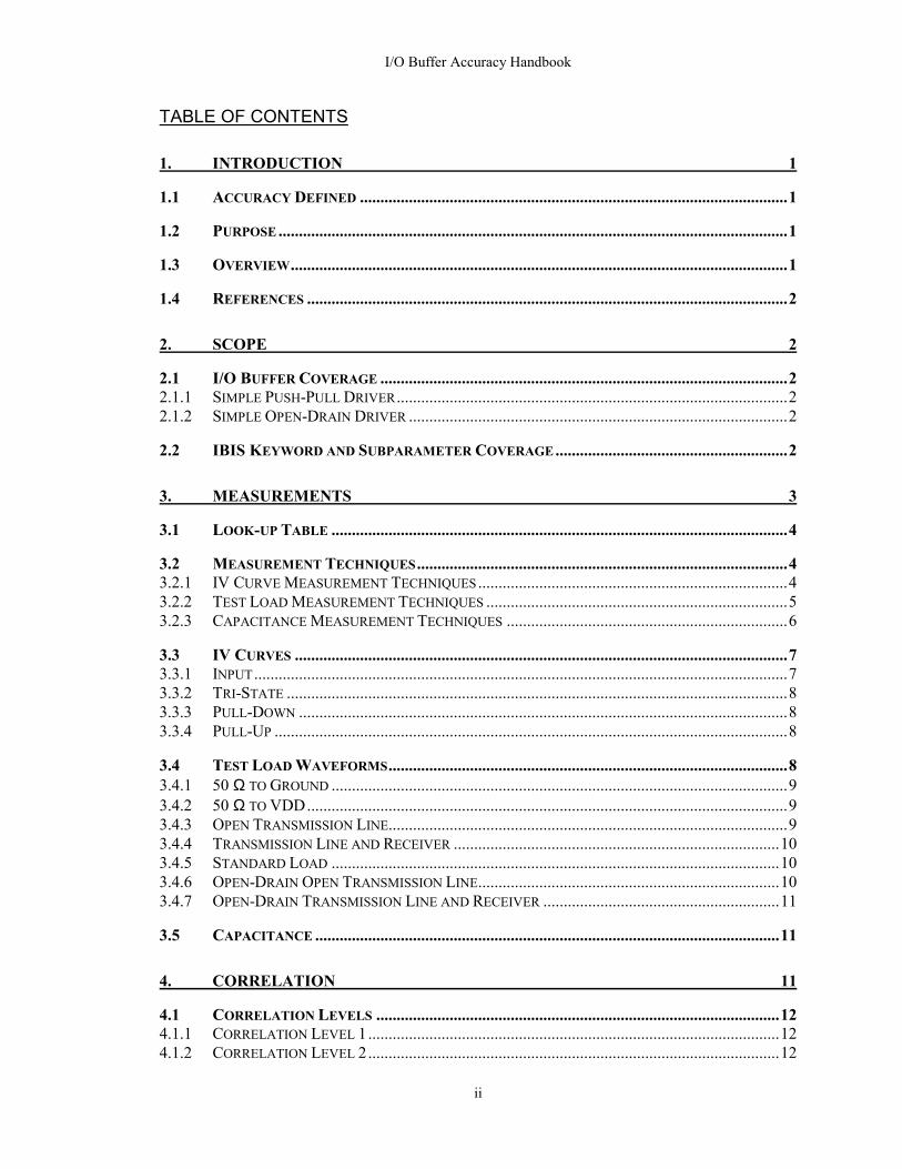
In the open transmission line load, it is important to design the transmission line impedance high enough relative to the drivers output impedance so as to create multiple reflections on the transmission line. This will facilitate cross-checking of the drivers complex reflection coefficient. For a typical 3.3 volt CMOS push-pull driver, the waveform should look similar to the one shown below.
0 1 2 3 4 5 6 7 8 9 10
time (ns)
0
1
2
3
4
5
6
Far-
end
Volta
ge (V
)
StrongWeak
Open-Ended Transmission Line
In the Transmission Line and Receiver load, the transmission line impedance should be high enough to allow the clamps to turn on, if they exist. Set the period of the input signal low enough to allow the waveform to settle out to its dc state before it begins switching again. Finally, only switch one output at a time. This will minimize any errors introduced by power and ground rail collapse when multiple outputs switch at the same time.
3.2.3 Capacitance Measurement Techniques
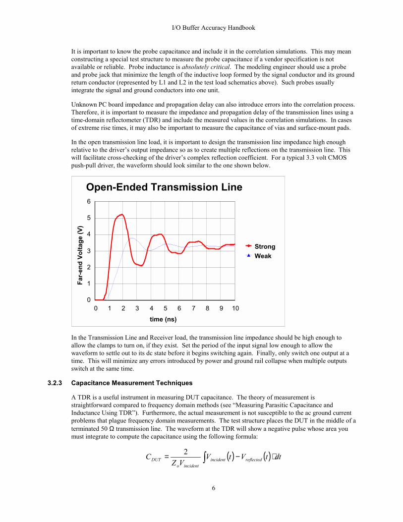
A TDR is a useful instrument in measuring DUT capacitance. The theory of measurement is straightforward compared to frequency domain methods (see Measuring Parasitic Capacitance and Inductance Using TDR). Furthermore, the actual measurement is not susceptible to the ac ground current problems that plague frequency domain measurements. The test structure places the DUT in the middle of a terminated 50 Ω transmission line. The waveform at the TDR will show a negative pulse whose area you must integrate to compute the capacitance using the following formula:
( ) ( ) ⋅−= dttVtVVZ
C reflectedincidentincidento
DUT2
I/O Buffer Accuracy Handbook
7
There are three important considerations related to accurately measuring capacitance using a TDR. First, the test trace should be sufficiently far away from neighboring traces as to make coupling insignificant. Make a simple crosstalk computation if youre not sure how close is too close. Second, the trace should be long enough relative to the TDR rise time so as to allow the operator to distinguish between the discontinuity of the test jack and the reflection from the. Third it is imperative the capacitance measurements be made while the DUT is powered up as semiconductor junction capacitances are bias-dependent IV curves.
3.3 IV Curves
The IV curves define the dc impedance characteristics of the I/O buffer. In the case of the simple push-pull output buffer, the IV curves are the drain current vs. drain-source voltage characteristics of the pull-up and pull-down FETs with a fixed gate voltage. In the case of a simple input buffer with clamp diodes, the IV curves are the diode terminal current vs. junction voltage characteristics, equivalent to the classical diode equation. IV curves are the simplest of the three categories of measurements, and they are essential for successful correlation of the other measurements.
The IV curve measurements cover the IBIS keywords Pulldown, Pullup, GND clamp, and POWER clamp.
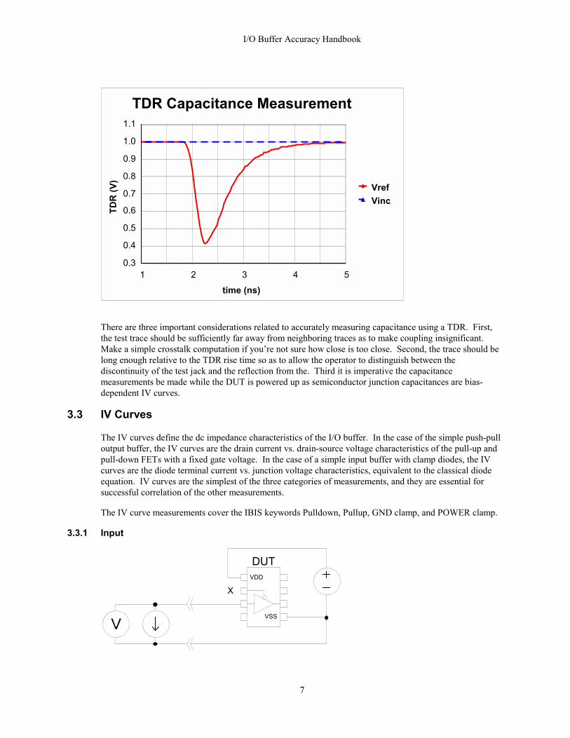
3.3.1 Input
VDD
VSS
DUT
X
1 2 3 4 5
time (ns)
0.3
0.4
0.5
0.6
0.7
0.8
0.9
1.0
1.1TD
R (V
)
VrefVinc
TDR Capacitance Measurement

I/O Buffer Accuracy Handbook
8
VDD
VSS
DUT
X
3.3.2 Tri-State
VDD
VSS
DUT
V
HX
3.3.3 Pull-Down
VDD
VSS
DUT
V
LL
3.3.4 Pull-Up
VDD
VSS
DUT
V
LH
3.4 Test Load Waveforms
The first two waveforms of interest are 50 Ω to ground and 50 Ω to VDD. Note that schematics for measurement 3.4.1 demonstrate two electrically equivalent loads that may be used interchangeably depending on board placement constraints.
The open transmission line tests the complex reflection coefficient of the driver, which is a combination of non-reactive components (represented by IV curves) and reactive components (die capacitance and package

I/O Buffer Accuracy Handbook
9
elements). The driver reflection coefficient is important when there are multiple reflections on a net and in cases where reflected reverse crosstalk is significant. The transmission line and receiver load tests the complex reflection coefficient of the receiver as well as the transient response of the clamp devices. Finally, the standard load represents the conditions the manufacturer deems to be most common. This load is less critical than the other four, but it is important in defining the timing parameters of the component.
3.4.1 50 ΩΩΩΩ to Ground
VDD
VSS
DUT
L
PROBE50
L1
L2
Ω SCOPE
VDD
VSS
DUT
L
PROBE
L2
L1
50 Ω
Ω50
SCOPE
3.4.2 50 ΩΩΩΩ to VDD
VDD
VSS
DUT
L
PROBE
L2
50 Ω
L1 SCOPE
3.4.3 Open Transmission Line
VDD
VSS
DUT
L Ω
PROBE
L1
L2
Z
SCOPE

I/O Buffer Accuracy Handbook
10
3.4.4 Transmission Line and Receiver
VDD
VSS
DUT
ΩZVDD
VSS
DUT
PROBE
L1L2
X
SCOPE
3.4.5 Standard Load
VDD
VSS
DUT
L
PROBESTD
LOAD
L2
L1
SCOPE
3.4.6 Open-Drain Open Transmission Line
VDD
VSS
DUT
L Ω
PROBE
L1
L2
Z
SCOPE
R Ω

I/O Buffer Accuracy Handbook
11
3.4.7 Open-Drain Transmission Line and Receiver
VDD
VSS
DUT
ΩZ
VDD
VSS
DUT
PROBE
L1L2
X
SCOPE
R Ω
3.5 Capacitance
4. Correlation Correlation is the process of making a quantitative comparison between behavioral simulation results and lab data. Section 4 defines the correlation process for IV curves and transient waveforms. It also describes how to compare data from capacitance and edge rate measurements.
There are in general two different kinds of correlation: lab measurement vs. structural simulation and behavioral simulation vs. structural simulation. One of the three correlation levels defined in this section
VDD
VSS
DUT
X
TDR50 Ω 50 Ω , L
Ω50
50 Ω , L

I/O Buffer Accuracy Handbook
12
applies only to lab measurement vs. structural simulation correlation. The other two correlation levels apply to both types of correlation.
In the case of the IBIS datasheet, correlation is a two-step procedure. In the first step, the semiconductor vendor correlates lab data against SPICE-based golden waveforms that are embedded in the IBIS datasheet in the form of voltage-time tables. In the second step, the user correlates behavioral simulation results against the same golden waveforms using his or her simulator of choice. This approach effectively decouples the behavioral simulator from the hardware and splits the correlation problem into independent components. However, we still recommend that the semiconductor vendor run behavioral simulations using the IBIS datasheet for one behavioral simulator. This will enable the modeling engineer to fine-tune the model data and ferret out possible discrepancies that would go otherwise unnoticed.
4.1 Correlation Levels
Model users have accuracy needs that vary with the demands imposed by their designs. For this reason, the I/O Buffer Accuracy Handbook defines several correlation levels. A correlation level is a means for categorizing model data by the amount of effort the modeling engineer invests in verifying their accuracy. Each individual correlation level is defined on the basis of how much the modeling engineer knows about the semiconductor processing conditions of the sample component(s). For the purposes of this handbook, a metric is simply a numerical method for quantifying how well two sets of data points agree with each other.
Table 3: Correlation Levels
Level Component Sample Envelope Metric
Overlay Metric
1 Random YES NO
2 Known typical YES YES
3 Known typical, fast, slow YES YES
4.1.1 Correlation Level 1
Correlation Level 1 applies in the case that the modeling engineer knows nothing about the processing conditions of the DUT. In other words, the DUT is a random sample. The Curve Overlay Metric only applies in cases where the two curves should theoretically lie on top of one another. Therefore, the Curve Envelope Metric is the only valid metric in this case. The Envelope Metric is not useful in all waveforms or IV curves (see section 4.4). Correlation Level 1 provides the least accuracy information. It is relevant to correlation of golden waveforms to lab measurements only.
4.1.2 Correlation Level 2
Correlation Level 2 applies in the case that the modeling engineer has a sample component that is known to come from a lot with typical semiconductor device parameters. The Envelope Metric applies in all Correlation Levels, but the Overlay Metric provides more accuracy information. Correlation Level 2 is relevant to correlation of golden waveforms to lab measurements and behavioral simulations.
4.1.3 Correlation Level 3
Correlation Level 3 applies in the case that the modeling engineer has three sample components: one from a lot with known typical semiconductor device parameters, one from a fast lot, and one from a slow lot. As in the previous two Correlation Levels, the Envelope Metric applies. Correlation Level 3 insures the highest degree of accuracy as well as confidence that the semiconductor vendor can indeed control the process in a

I/O Buffer Accuracy Handbook
13
manner consistent with the model data. This allows the model user to have confidence in the timing and noise margins of the system he or she is designing. Correlation Level 3 is relevant to correlation of golden waveforms to lab measurements and behavioral simulations.
4.2 Correlation Considerations
4.2.1 Voltage and Temperature Conditions
The three correlation levels defined above address the semiconductor processing conditions of the sample component, but they do not address operating voltage and temperature. Voltage is easy to measure; temperature is not. It is possible for the modeling engineer to measure junction temperature by observing the characteristics of a semiconductor device (such as a diode) or by measuring the power the device draws for a known junction-to-case thermal resistance (θjc).
When correlating lab data and simulation results using the Overlay Metric, it is important that the voltage and temperature conditions in both sets of data match as closely as possible. When using the Curve Envelope Metric, it is important that the voltage and temperature conditions are within the boundaries used to create the golden waveforms. In either case, the modeling engineer should document the voltage and temperature conditions.
4.2.2 I/O Cell Coverage
It is up to the discretion of the modeling engineer to decide which I/O cell designs warrant correlation. For example, a gate array I/O cell library may contain hundreds of cell designs, many of which are similar to one another. In this case, the modeling engineer may choose a sample that represents a family of I/O cells. It is important that the modeling engineer document which I/O cells he or she correlated.
4.3 Curve Overlay Metric
The Curve Overlay Metric applies to cases in which the measured and simulated data should theoretically lie directly on top of each other. For example, a structural simulation of a 50 Ω load and a behavioral simulation of the same load should theoretically yield identical results. Another example is the measurement of a known-typical sample component and a structural simulation of the same network under identical process-voltage-temperature conditions. The Curve Overlay Metric measures how well the two curves or waveforms match each other by summing the absolute value of the x-axis (or y-axis) differences between the two data points, weighing the sum against the range of data points along that axis, and dividing by the number of data points.
( ) ( )
⋅∆−
−⋅= =
NXDUTXgoldenX
FOMN
i ii11100
A small C program or script could compute the Figure of Merit defined in the above equation. The first numerical task that the algorithm must carry out is to map each set of data points to a common x-y grid by interpolation. The second task is to slide one curve against the other along the x-axis. In the case of the IV curve, this is a trivial step because the two curves are already aligned, but the x-axis origin is an arbitrary point in the case of voltage-time waveforms. Once this is accomplished, the algorithm can then perform the third and final step: comparing the data points and calculating the figure of merit.
The example below demonstrates two voltage-time waveforms that have identical edge rates but slightly different corners. The first plot shows the original raw data. The second plot shows the same two waveforms after x-axis adjustment. The bold lines are y-axis error bars, i.e. the difference between the two curves in the y direction. The third plot shows the x-axis error bars.
I/O Buffer Accuracy Handbook
14
4.4 Curve Envelope Metric
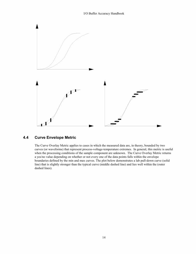
The Curve Overlay Metric applies to cases in which the measured data are, in theory, bounded by two curves (or waveforms) that represent process-voltage-temperature extremes. In general, this metric is useful when the processing conditions of the sample component are unknown. The Curve Overlay Metric returns a yes/no value depending on whether or not every one of the data points falls within the envelope boundaries defined by the min and max curves. The plot below demonstrates a lab pull-down curve (solid line) that is slightly stronger than the typical curve (middle dashed line) and lies well within the (outer dashed lines).

I/O Buffer Accuracy Handbook
15
The Curve Envelope Metric presents a difficulty in the case of unterminated transmission line loads. Because these waveforms overshoot normal logic levels and ring back, the min and max waveforms intersect each other and do not define an envelope. Therefore, the Curve Envelope Metric may not be applied to the Open Transmission Line load or the Transmission Line and Receiver load.
4.5 Capacitance
The modeling engineer should compare lab capacitance measurements against the datasheet specifications and the applicable model format (SPICE or IBIS). The model data frequently disagree with each other and the datasheet specification, and the customer needs to be aware of these discrepancies. The lab measurements should lie between the minimum and maximum values in all three cases.
Table 4: Capacitance Example
Cpin min lab max units
Datasheet pF
SPICE pF
IBIS pF
4.6 Edge Rate
The figure below demonstrates how to measure dV/dt using the 50 Ω to VDD test load. The 20% and 80% lines are relative to the loaded dc high level rather than the unloaded dc high level. Like the capacitance measurements, the lab edge rates should lie between the minimum and maximum values in all three cases.
-5 0 5 10Vout (V)
-150-100-50
050
100150200250
Iout
(mA
)
Envelope Metric

I/O Buffer Accuracy Handbook
16
Table 5: Edge Rate Example
dV/dt Rise min lab max units
Datasheet V/ns
SPICE V/ns
IBIS V/ns
5. Documentation Documentation is the final step in the model accuracy process outlined in this document; it is critical. The actual format of the documentation may vary from vendor to vendor. For this reason we have chosen to provide two examples that may serve as templates: the I/O Buffer Accuracy Report and the IBIS Accuracy Trailer.
80%
20%
t∆
V∆

I/O Buffer Accuracy Handbook
17
Glossary Accuracy: Agreement between behavioral simulation results and lab measurements.
Behavioral Model: An I/ O buffer model, consisting of a circuit network and corresponding set of equations, in which ideal sources and lumped elements replace semiconductor devices. Behavioral models are not necessarily as common among behavioral simulators as the BSIM or Gummel-Poon transistor models are common among SPICE simulators.
Correlation: The process of making a quantitative comparison between two sets of I/O buffer characterization data, e.g. lab measurement vs. structural simulation or behavioral simulation vs. structural simulation.
Correlation Level: A means for categorizing I/O buffer characterization data based on how much the modeling engineer knows about the processing conditions of a sample component and which correlation metric he or she used.
Correlation Metric: A means for quantifying agreement between two sets of curves. The Curve Overlay Metric associates a figure of merit with two curves. The Curve Envelope Metric indicates whether or not the lab data fell within the envelope defined by the simulation data.
DUT: Device-under-test.
Figure of Merit: A percentage that indicates the goodness of fit between two curves using the Curve Overlay Metric. A figure of merit of 100% indicates ideal correlation.
Golden Waveform: A voltage-time table in the IBIS datasheet that stores SPICE simulation results for a specified load using the IBIS [Rising Waveform] and [Falling Waveform] syntax. Golden Waveforms are not to be confused with the voltage-time tables used by simulators to adjust their internal stimulus. These waveforms require a non-reactive load.
IBIS: I/O Buffer Information Specification. A template for communicating information about the electrical characteristics of an I/O buffer.
IBIS Accuracy Trailer: A comment section appended to the end of an IBIS datasheet that contains the correlation results (figure of merit table) and some information regarding the test environment.
IBIS Datasheet: The ASCII text file that conforms to the I/O Buffer Information Specification and contains the input data for a behavioral simulation. In common conversation, the terms IBIS datasheet and IBIS model are often used interchangeably, which can lead to confusion about exactly what information an IBIS datasheet contains. See Behavioral Model.
Known Typical Sample: A sample component that process or device engineers have identified as lying in the center of the device parameter distributions. Such identification is usually accomplished by means of parametric measurements on a test site common to every wafer. Known fast or known slow samples are also possible but less common.
Modeling Engineer: An employee of the semiconductor company who carries out the analysis necessary to generate a SPICE model or IBIS datasheet from source data. The modeling engineer must have sufficient circuit analysis background to make decisions about how the relevant electrical characteristics of the I/O buffer are represented by the model data.
Random Sample: A sample component of unknown process origin.
Sample Component: The DUT that the modeling engineer uses to make lab measurements for correlation with simulation results.

I/O Buffer Accuracy Handbook
18
Structural Model: An I/O buffer model in which each device (transistor, resistor, diode, etc.) in the circuit is represented by an element in a netlist. In turn, each element must reference a physical device model, which comprises a set of parameterized current-voltage equations. The structural model has three components: the netlist of the circuit, the device equations, and the device equation parameters. The most common language for encoding structural models is SPICE (Simulation Program with Integrated Circuit Emphasis, from the University of California at Berkeley).

I/O Buffer Accuracy Handbook
19
Appendix A: SPICE Model Checklist
1. Is the SPICE model in subcircuit format?
2. Was the SPICE subcircuit extracted from the I/O cell layout?
3. Does the ESD diode model represent the correct IV, capacitance, and stored charge behavior?
4. Does the SPICE model include fast, slow, and typical transistor model parameters?
5. Does the SPICE model use MKS units for compatibility with other vendors models?
6. Does the SPICE model include an unencrypted single-pin package subcircuit that can be called separately from the I/O buffer subcircuit?
7. Is the SPICE model free from any extraneous off-chip loads that may have been used during testing?
8. Are the correct pin voltages documented for all pins?
9. Are the driver input rise and fall times documented?
10. Are fast, slow, and typical temperatures and VDD documented?
11. Has the modeling engineer tested the SPICE model?
12. Has the modeling engineer included a running example input deck?

I/O Buffer Accuracy Handbook
20
Appendix B: IBIS Datasheet Checklist
1. Does the IBIS datasheet pass the IBIS syntax checker? (Note: Some models generate warnings for non-monotonicities that are actually part of the characteristics of the device. Other non-monotonicities are so small as to be irrelevant.)
2. Do the keywords Cref, Rref, Vref, and Vmeas match the values specified in the component datasheet for all output and bidirectional models?
3. Does the output reach Vmeas for rising and falling waveforms? 4. Do the keywords Vihl and Vinh represent the unity gain points derived from the dc transfer
characteristics for all inputs? 5. Does the pin table match the component datasheet? 6. Does each entry in the pin table have a unique signal name and pin number? 7. Do all models called out by the pin table exist in the IBIS datasheet? 8. Has the modeling engineer verified the accuracy of the C_comp subparameter? 9. Has the modeling engineer verified the accuracy of the R_pkg, L_pkg, and C_pkg subparameters? 10. Does MIN and MAX data exist? 11. For CMOS logic, do all MAX data represent maximum voltage, minimum temperature, and fast
process? 12. For CMOS logic, do all MIN data represent minimum voltage, maximum temperature, and slow
process? 13. For bipolar logic, do all MAX data represent maximum voltage, maximum temperature, and fast
process? 14. For bipolar logic, do all MIN data represent minimum voltage, minimum temperature, and slow
process? 15. Do the keywords dV/dt_r and dV/dt_f contain the correct 20%-80% edge rate data measured using a
50 Ω load as specified in IBIS? 16. Does the IBIS datasheet include all four 50 Ω VT tables as described in the IBIS Cookbook? 17. Has the modeling engineer performed a visual inspection of IV and VT curves to screen for non-
monotonicity, discontinuities, and other obvious errors? 18. Has the modeling engineer tested the IBIS datasheet using a behavioral simulator? 19. If the I/O buffer employs dynamic clamping, does the IBIS datasheet contain the appropriate
keywords and subparameters? 20. If the I/O buffer employs a multi-stage driver, does the IBIS datasheet contain the appropriate
keywords and subparameters? 21. Does the I/O buffer employ dynamic edge rate control, dynamic impedance control, or any form of
feedback?

I/O Buffer Accuracy Handbook
21
Document History NOTE: The original title of this document was the IBIS Accuracy Specification. We changed the name to I/O Buffer Accuracy Handbook to include SPICE models.
The idea for an IBIS Accuracy Specification was hatched at the December 1997 meeting of the IBIS Users Group in Chelmsford, Massachusetts. Many of the attendees expressed strong concerns regarding the accuracy of presently available IBIS datasheets, and a subcommittee quickly formed with the mission of producing an IBIS Accuracy Specification in one years time. The members of the IBIS Accuracy Subcommittee are Fawn Engelmann (CAE Engineer, EMC), Robert Haller (Hardware Principle Engineer, Compaq Computer), Bruce Heilbrunn (Signal Integrity Engineer, Stratus Computer), Peter LaFlamme (Applications Engineer, Fairchild Semiconductor), Harvey Stiegler (Senior Member Technical Staff, Texas Instruments), and Greg Edlund (Advisory Engineer, IBM Corporation and subcommittee chairman). The IBIS Accuracy Subcommittee and the signal integrity community at large owe a debt of gratitude to EMC and Fairchild Semiconductor for providing the resources to design and build two accuracy test boards.
The challenge of writing any specification is to clearly state only what is necessary in such a way as to minimize the opportunity for misinterpretation (which will happen occasionally in even the best-written specifications). Writing the IBIS Accuracy Specification presented some unique challenges, such as bringing IBIS accuracy from the conceptual realm into the quantitative realm. The word accuracy conjures up a vague concept of agreement between simulations and data from test hardware; what exactly does this mean, and how can one quantify accuracy?
In the process of defining IBIS accuracy quantitatively, one of the first questions the IBIS Accuracy Subcommittee had to address was scope. The effectiveness of the IBIS Accuracy Specification lies in its ability to cover the relevant electrical behavior of a given driver family. Each unique driver family requires a certain set of IBIS keywords for accurate behavioral modeling, and each unique driver family might require a unique set of test loads to elucidate the electrical behavior of that driver family. For example, modeling the circuit behavior of a simple push-pull CMOS driver requires the basic IBIS keywords: Pulldown, Pullup, GND clamp, POWER clamp, C_comp, C_pkg, Ramp, Rising Waveform, and Falling Waveform. Modeling the circuit behavior of a multi-stage driver requires additional keywords. What set of test loads will sufficiently cover the relevant electrical behavior of each of these types of drivers?
Another question that presented itself was how much detail to include regarding measurements. For example, when a modeling engineer is measuring dV/dt for a 0.5 ns edge, oscilloscope and probe bandwidth play a critical role in determining the accuracy of the measurement. However, the subcommittee did not wish to write a specification that was only relevant to a narrow set of test equipment. Which features of the test environment are necessary elements of the specification?
One topic that arose repeatedly during discussions of the IBIS Accuracy Subcommittee was the effects on IBIS accuracy of the simulator. Even if a modeling engineer goes to great lengths to verify the accuracy of a given IBIS datasheet on a given simulator, it is possible that the lab data may not agree with results obtained using another simulator. Each simulator must translate the IBIS datasheet into its own native model format before a simulation can begin, and this translation process is one potential source of discrepancies among simulators. Furthermore, each simulator uses its own unique numerical algorithms to arrive at the circuit solution. How could the IBIS Accuracy Subcommittee craft a specification that was independent of simulator platform?
The IBIS Accuracy Test Board is a companion to this specification. Its purpose is to demonstrate one possible set of test structures that facilitate measurement of the ac and dc parameters specified in this document. The schematics, Gerber files, parts list, and application note are available on the web sites listed in the Reference section. The board design is free. The IBIS Accuracy Subcommittee encourages any interested party to study, improve, and freely share the design to further the understanding of the IBIS Accuracy Specification.


