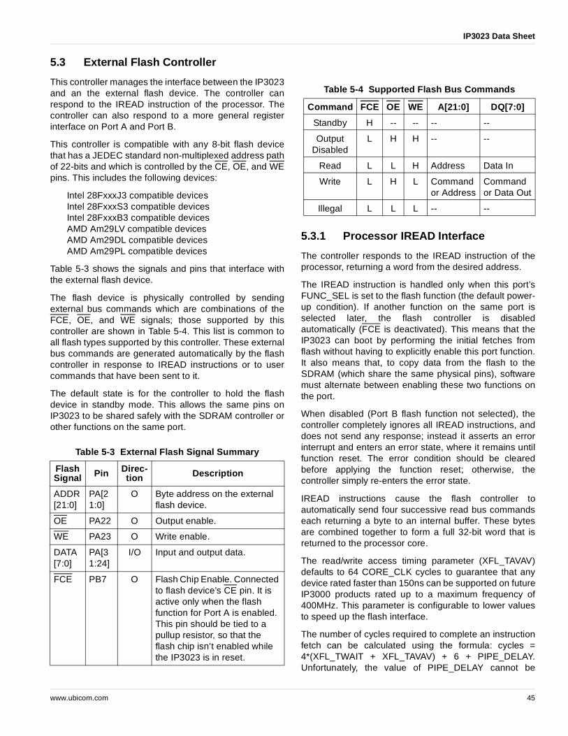
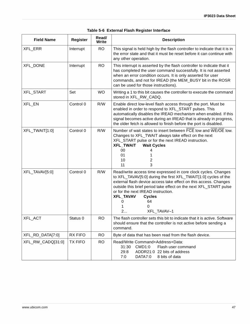
Key Features:• 32-bit Mutithreaded CPU, in 250 MIPS and 325 MIPS versions• IP3023 is optimized for wireless networking
• Eight-way simultaneous multithreading• Deterministic execution on all threads• Zero overhead full context switching• Programmable MIPS per thread• Optimized ISA for packet processing
• Memory-to-memory architecture, powerful addressing modes• Small, fast instruction set, strong bit manipulation• Reduced code size vs. RISC CPUs
• On-chip program and data memory• Eliminates cache miss penalties• 256 KB (64K x 32) of program SRAM• 64 KB (16K x 32) of data SRAM
• Highly configurable I/O support• Many combinations of software I/O:
• True random number generator for software-implemented encryption/security (32-bit seed)
• Fixed-point MAC (16x16+48-bit, 250/325 MMACs) for voice/audio codecs, other signal processing tasks
• Independent I/O and core CPU clocking • Separate phase-locked loops (PLLs)• Programmable multipliers & dividers• Single low-cost crystal (10–20 MHz)
Figure 1-1 IP3023 Block Diagram
CLK CNTRL(PLL Mult
I/O and Sys)
8-WAY MULTI-THREADED32-BIT CPU
64K x 32INSTRUCTION
RAM
16K x 32DATARAM
SYSTEM,REAL-TIME,WATCHDOG
TIMERS
MII x 4(host and phy)
SerDes x 2 (10BT, USB, SPI, UART,
etc.)
SDRAMCONTROLLER
RANDOMNUMBER
GENERATOR
IP3023
I/O PORT SELECTOR
GPIO (802.11x CardBus, Utopia, PCM, I2C, PCMCIA, ISA, etc.
possible)
FLASHCONTROLLER
32
PORT A
8
PORT B
16
PORT C
18
PORT D
16
PORT H
32
PORT G
8
PORT F
8
PORT E
SYSTEMANDI/O
CLOCKS
IP3K-DDS-002.eps
High-SpeedGPSI
The IP3023™ wireless network processor is arevolutionary new platform from Ubicom designed toprovide highly integrated solutions for applications at the“edge” of Internet connectivity, including 802.11a/b/gaccess points, routers, hot spots, bridges, gateways, anda wide variety of embedded networked client solutions.The IP3023 is optimized for efficient network processingin embedded solutions. Its development has led to thedefinition of a new microprocessor architecture:Multithreaded Architecture for Software I/O (MASI). ManyMASI concepts were pioneered in the Ubicom IP2000™family of processors, but the IP3023 dramatically extendsthose techniques by introducing hardware support formultiple threads operating with no context switchingoverhead, as well as three-operand and memory-to-memory operations.
The IP3023 is a 250- or 325-MIPS 32-bit CPU supportingeight-way multithreaded operation. It provides for up toeight real-time tasks to execute in a completelydeterministic fashion. In essence, the IP3023 supportsrunning a different thread on every clock, but without theoverhead for context switching typical with traditionalmicroprocessor architectures. To the system designer, theIP3023 appears as if there were eight processors on thechip.
m, Inc. All rights reserved. 1
IP3023 Data Sheet
The multithreaded and deterministic nature of the IP3023processor provides for integration of numerous functionson chip – some with on-chip hardware assist and someentirely in software – as threads, including the ability tosupport interfaces such as 10/100 MII and 10Base-TEthernet MAC/PHY, USB, GPSI, Utopia, PCMCIA, IDE,PCM Highway, and CardBus/Mini PCI interface specificfor 802.11a/g wireless radios. This yields both a highdegree of flexibility and reduces die size, as it eliminatesthe need for many on-chip dedicated hardware blocks forspecific functions.
The IP3023 employs a three-operand and memory-to-memory architecture, utilizing on-chip program and datamemory support. This scheme enables highly efficientdata movement and processing on data. The result is thatthe IP3023 is designed to support packet processing andtransfers at wire speeds, eliminating the need for cachesand large data buffers typically found in use withtraditional RISC-based microprocessors.
To further optimize the IP3023 for networkinginfrastructure and embedded client solutions, theprocessor includes several key hardware support blocks,including true random number generator and fixed-pointmultiply/accumulate (MAC) units. The random numbergenerator facilitates robust software implementation ofcommon encryption/security protocols critical to thecontinued growth of wireless networking. The MAC unitsupports implementation of voice/audio codecs and othersignal processing tasks.
Foundation for Highly Flexible Connectivity Solution
• Performance: 250 MIPS @ 250MHz,325MIPS @ 325MHz
• 250/325 MMACs performance from MAC unit withfixed point 16x16 multiply and 48-bit accumulator.
• On-chip dual-ported SRAM data memory.• On-chip SRAM program memory.• On-chip hardware for zero overhead instruction level
context switch for multithreading.• In-system programming of external flash.
Multiple Networking Protocols and Physical Layer Support Hardware
• Two full-duplex serializer/deserializer (SerDes)channels.– Flexible to support 10Base-T, GPSI, SPI, UART,
USB protocols.– One on-chip PHY function for 10Base-T Ethernet.
• Four MII Ports, each can operate in host or phy mode.
Memory
• 256 KB (64K x 33) on-chip program SRAM with 1-bitparity.
• 64 KB (16K x 32) on-chip dual port data SRAM.• Up to 4 MB (4M x 8) off-chip flash support.• Up to 64 MB (32M x 16) off-chip PC 66/100/133
SDRAM support.
IP3023 Wireless Network Processor Features
• 32-bit data and instruction paths (fixed instructionwidth).
• Instructions execute at the rate of one per clock cycle.• Eight-way instruction level multithreading with
support for both hard real time and non-real-timethread priority scheduling.
• Multiply and multiply/accumulate (MAC) instructions,where MAC uses a 48-bit accumulator.
• Special purpose CRC instruction for CRCgeneration/checking and encryption.
• Sixteen general-purpose 32-bit registers per thread(128 total).
• Eight 32-bit address registers per thread (64 total).• High instruction code density.
General-Purpose Hardware Peripherals
• True random number generator (32-bit seed number).• One 32-bit system timer synchronous with system
clock with eight compare registers.• One 32-bit real-time timer (one mode of the
Multipurpose Timer) with constant clock frequency.• Watchdog 32-bit timer with constant clock frequency.
• Power-on reset circuit.• Eight external interrupt inputs mapped to I/O ports.• Two programmable output clocks.
Sophisticated Power and Frequency/Clock Management Support
• Operating voltage from 1.14V to 1.26V.• Single clock input with 10–20 MHz crystal clock input
support.• Two on-chip PLLs: one for processor clock, one for
serial I/O.• Core clock using a selectable on-chip divider.• Software CPU speed control for power saving.• Power-on reset (POR) logic.• Auxiliary I/O clock input for serial I/O PLL.
• Customer application program updatable.– Run-time self programming.
• On-chip in-system debugging support interface.• Debugging at full IP3023 operating speed.
Complete Software Development Environment
The IP3023 wireless network processor is capable ofsupporting the following functions in software. See aUbicom sales representative for availability and schedule.
complete software solutions and platform for wireless routers, access points, bridges, print servers, network cameras, and many other embedded network client applications. Includes core networking stack, numerous wired and wireless PHY layers and interfaces, plus application layer ipModules for WebServer, DNS, SMTP email, SNMP remote management, DHCP client/server, and NAT routing, to name a few.
• Red Hat® GNUPro® tools.– Includes GCC ANSI C compiler and assembler,
linker, utilities, and GNU debugger.• Configuration tool.
– Integrated tool to support rapid development efforts.• Ubicom’s Unity™ integrated development
environment (IDE).– Includes editor, project manager, graphical user
interface to GNU debugger, device programmer, ipModule configuration tool, and profiler.
• Profiler for performance tuning.
4 www.ubicom.com
IP3023 Data Sheet
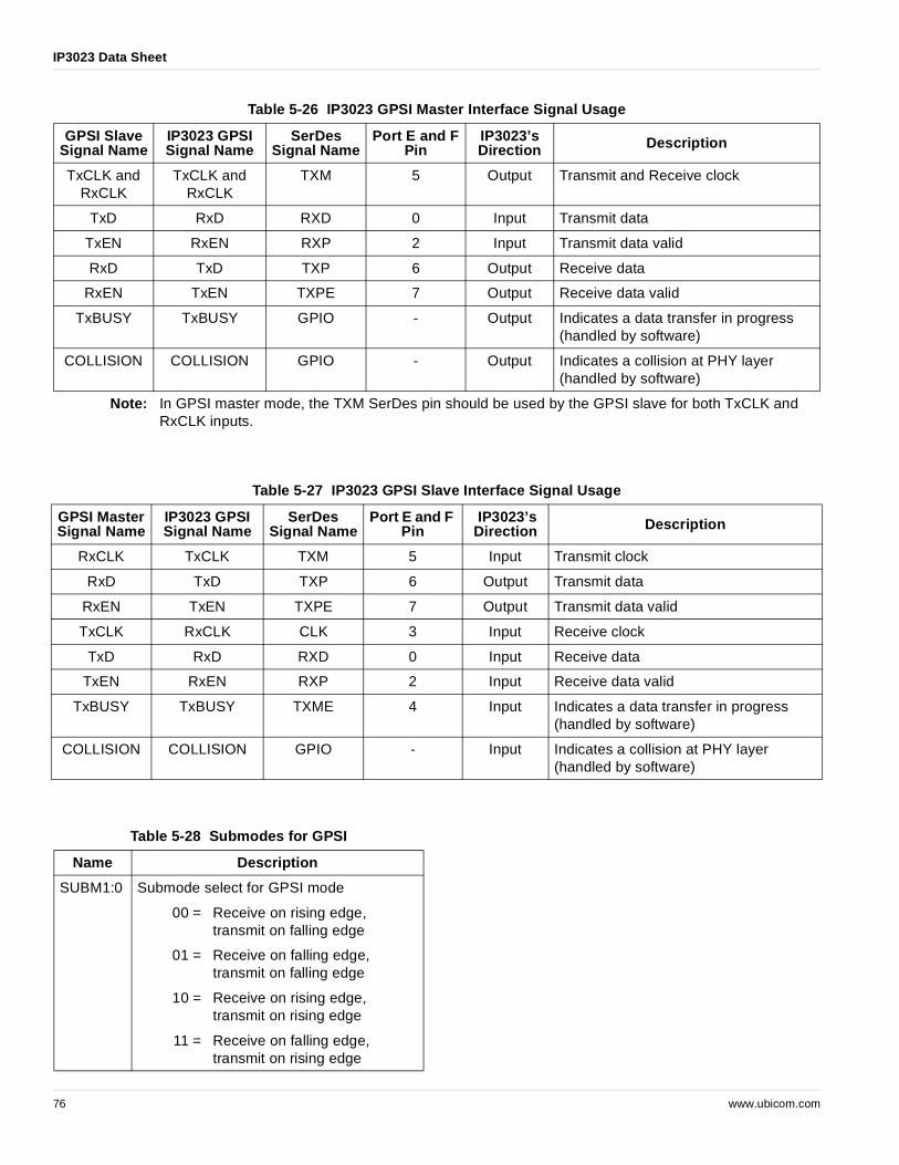
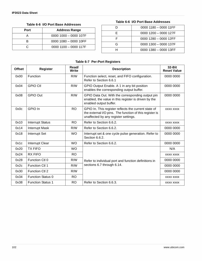
1.2 I/O Port Mapping
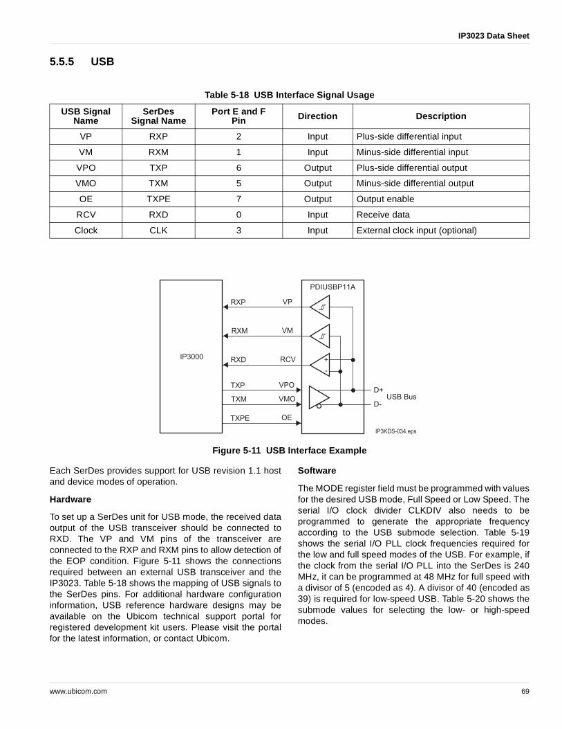
The IP3023 has highly configurable port mapping. Port A,for example, supports the external flash, but can also beshared with the SDRAM controller and a PCMCIAinterface when combined with Port B. Some of the portsshare a dedicated hardware function. Port E, for example,shares a part of an MII port, one of the on-board SerDesunits, or part of a Utopia bus implementation in software.All ports (except Port A) can be used as GPIO ports,giving up to 106 GPIO pins. GPIO ports are used to createvirtual I/O ports to control UTOPIA, 802.11a/b/g, PCMHighway, and other popular interfaces. Table 1-1 showshow the IP3023 I/O ports are shared and shows possibleI/O port mappings for three different applications.
1.3 Architecture
1.3.1 CPU
The CPU is a general-purpose 32-bit pipelined processor.The CPU implements multithreading in hardware andsupports the execution of deterministic hard real-time(HRT) threads. Up to eight simultaneous threads aresupported in hardware. Code for the processing core iswritten in C as well as in assembly language.
1.3.2 CPU Instruction Memory
The instruction memory for the main processor isimplemented as a single-port (256 KB with parity,64K x 32) SRAM. This RAM is able to supply the mainprocessor with one instruction access per clock.
1.3.3 CPU Data Memory
The data memory for the main processor is 64 KB (16K x32) SRAM. It is able to perform one read and one write perclock, in support of the three-operand and memory-to-memory instruction set architecture.
1.3.4 Clocks, Frequency, and Timers
A single clock input (crystal, 10–20 MHz) is used to sourcemultiple subsystems and peripherals in the IP3023. Thisclock source is fed into independent PLLs for generatinga system clock and a serial I/O clock. Alternatively, thePLLs can be bypassed, and the 10–20 MHz clock inputcan be used directly. The PLLs are capable of generatingup to a 250 MHz core clock from the 10–20 MHz inputsignal, or up to 325MHz on the 325MHz rated version.
This 10–20 MHz input is also fed into a real-time clock(RTC) timer portion of the multipurpose timer, which canbe used to maintain an accurate time base in a system.
Table 1-1 I/O Ports and Example Configurations
I/O Port Port Width(bits)
Actual Hardware I/O Support
Dual / Multimode Access Point
Print ServerBridge
Networked Embedded Devices
Port A 32 Flash Flash Flash Flash
Port B 8 SDRAM GPIO / SDRAM (opt.) GPIO / SDRAM (opt.) GPIO / SDRAM (opt.)
Port C 16 MII GPIO GPIO GPIO
Port D 18 MII MII MII MII
Port E 8 SerDes or MII (1/2)or Hi-Speed GPSI.
GPOI GPIO GPIO
Port F 8 SerDes or MII (1/2) GPIO USB GPIO
Port G 32 GPIO 802.11(a and g)
802.11(a or g)
802.11(a or g)Port H 16 MII
www.ubicom.com 5
IP3023 Data Sheet
1.3.5 Reduced Power Operation
The IP3023 can be configured for lower power operationby varying the frequency of operation and clock source.These lower power modes include:
• Reducing the clock frequency from the system clockPLL. The clock circuit of the IP3023 includes a run-time controllable CPU clock, which allows thedeveloper to reduce operating frequency (see Figure3-3).
• Turning off system clock PLL. System clocking runsdirectly from the 10–20 MHz clock input.
1.3.6 Interrupts
The IP3023 provides a flexible interrupt structure. Real-time interrupts are individually assigned to independentthreads. An interrupt awakens the corresponding thread,if it was waiting, and the thread handles the interrupt withthe priority and processor cycles assigned to the thread. Ifneeded, the structure of a traditional interrupt serviceroutine (ISR) can be emulated.
1.3.7 Reset
The following sources are capable of causing a chip reset:
• Power-on• Debug port• Watchdog timer (one mode of the multipurpose timer)• Parity error in on-chip instruction memory• External reset (RST pin)
1.3.8 Programming and Debugging
The IP3023 device has advanced in-system programmingand debug support on-chip. This unobtrusive capability isprovided through a Debug Interface. There is no need fora bond-out chip for software development. This eliminatesconcerns about differences in electrical characteristicsbetween a bond-out chip and the actual chip used in thetarget application. Designers can test and revise code onthe same part used in the actual application.
Ubicom provides the complete Red Hat GNUPro tools,including C compiler, assembler, linker, utilities, and GNUdebugger. In addition, Ubicom offers an integratedgraphical development environment which includes aneditor, project manager, graphical user interface for theGNU debugger, device programmer, ipModuleconfiguration tool, and profiler.
1.3.9 Other Supported Functions
• Random-number generator. The IP3023 includes anon-chip hardware true random number generator. On-chip random noise generates random bits which areaccumulated in a hardware 32-bit linear feedbackshift register (LFSR). This function can be used toseed a software random number generator or togenerate per-session cryptography keys.
• Boot from external flash. Unlike the IP2000 familyprocessors, there is no on-chip flash. At start-up, theIP3023 is configured to execute instructions from itsexternal flash port.
6 www.ubicom.com
IP3023 Data Sheet
2.0 Pin Definitions
2.1 228-Pin BGA
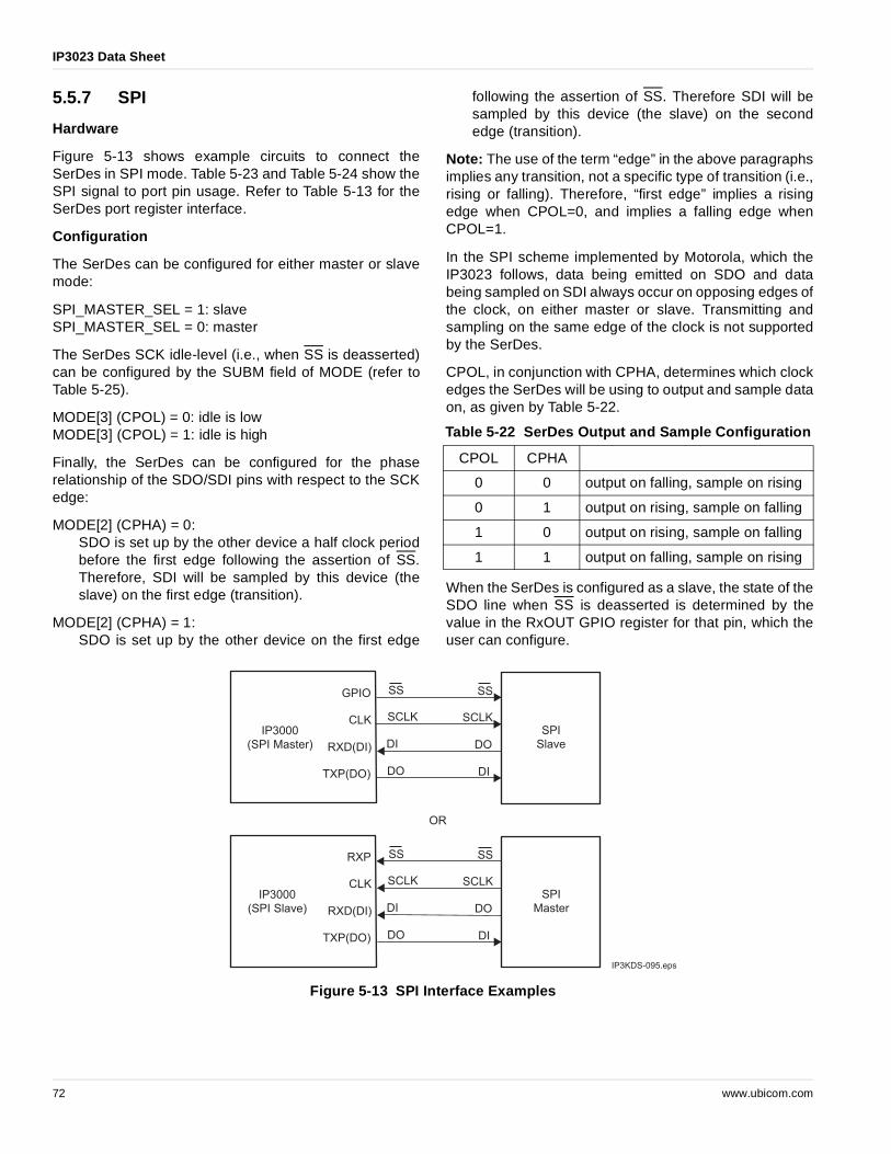
Figure 2-1 IP3023 BGA Pin Definition (Top View)
PB6
PB7
PE2
PE4
PE5
PF0
PF1
PF5
PF7
TEST2
PLL2VDD
PLL1VDD
OSC_IN
OSC_OUT
A2VDD
TEST1
PB1
PB2
PB3
PB5
PE0
PE3
PE7
PF3
PF6
PLL2VSS
IOVSS
A1VDD
A1VSS
A2VSS
TEST0
RST
PA27
PA30
PA31
PB0
PB4
PE1
PE6
PF2
PF4
PLL1VSS
IOVDD
PFRDN
PFRDP
TSS
TSI
PD17
PA24
PA26
PA28
PA29
DVDD
DVDD
IOVDD
IOVDD
DVDD
IOVDD
IOVDD
DVDD
TSCK
TSO
PD0
PD2
PA21
PA23
PA25
IOVDD
IOVDD
PD1
PD3
PD4
PA19
PA20
PA22
DVDD
IOVSS
IOVSS
DVSS
IOVSS
IOVSS
DVDD
IOVDD
PD5
PD6
PD7
PA16
PA17
PA18
IOVDD
IOVSS
IOVSS
DVSS
DVSS
IOVSS
IOVSS
DVDD
PD8
PD9
PD10
PA13
PA14
PA15
DVDD
DVSS
DVSS
DVSS
DVSS
DVSS
DVSS
DVDD
PD12
PD13
PD11
PA12
PA11
PA10
DVDD
DVSS
DVSS
DVSS
DVSS
DVSS
DVSS
DVDD
PD16
PD15
PD14
PA9
PA8
PA7
IOVDD
IOVSS
IOVSS
DVSS
DVSS
IOVSS
IOVSS
IOVDD
PC2
PC1
PC0
PA6
PA5
PA4
DVDD
DVDD
IOVSS
DVSS
IOVSS
IOVSS
IOVSS
DVDD
PC6
PC4
PC3
PA3
PA2
PA0
DVDD
DVDD
PC9
PC7
PC5
PA1
PH15
PH13
PH11
IOVDD
IOVDD
DVDD
IOVDD
IOVDD
DVDD
IOVDD
IOVDD
PG0
PC12
PC10
PC8
PH14
PH12
PH9
PH8
PH3
PG31
PG27
PG23
PG18
PG14
PG10
PG5
PG3
PG1
PC13
PC11
PH10
PH7
PH6
PH4
PH1
PG30
PG26
PG22
PG19
PG15
PG12
PG8
PG6
PG4
PC15
PC14
PH5
PH2
PH0
PG29
PG28
PG25
PG24
PG21
PG20
PG17
PG16
PG13
PG11
PG9
PG7
PG2
A
B
C
D
E
F
G
H
J
K
L
M
N
P
R
T
1 2 3 4 5 6 7 8 9 10 11 12 13 14 15 16
1 2 3 4 5 6 7 8 9 10 11 12 13 14 15 16
A
B
C
D
E
F
G
H
J
K
L
M
N
P
R
T
IP3023
Top View Through Package
www.ubicom.com 7
IP3023 Data Sheet
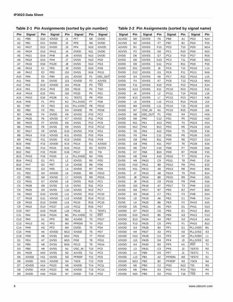
Table 2-1 Pin Assignments (sorted by pin number)
Pin Signal Pin Signal Pin Signal Pin Signal A1 PB6 D10 IOVDD J1 PF7 N8 DVDD
A2 PB1 D11 DVDD J2 PF6 N9 DVDD
A3 PA27 D12 DVDD J3 PF4 N10 IOVDD
A4 PA24 D13 PH11 J4 DVDD N11 DVDD
A5 PA21 D14 PH8 J6 IOVSS N12 DVDD
A6 PA19 D15 PH4 J7 DVSS N13 PG0
A7 PA16 D16 PG29 J8 DVSS N14 PG3
A8 PA13 E1 PE5 J9 DVSS N15 PG6
A9 PA12 E2 PE0 J10 DVSS N16 PG11
A10 PA9 E3 PB4 J11 IOVSS P1 OSC_OUT
A11 PA6 E4 DVDD J13 IOVDD P2 A2VSS
A12 PA3 E13 IOVDD J14 PG18 P3 TSS
A13 PA1 E14 PH3 J15 PG19 P4 TSO
A14 PH14 E15 PH1 J16 PG20 P5 PD1
A15 PH10 E16 PG28 K1 TEST2 P6 PD5
A16 PH5 F1 PF0 K2 PLL2VSS P7 PD8
B1 PB7 F2 PE3 K3 PLL1VSS P8 PD12
B2 PB2 F3 PE1 K4 IOVDD P9 PD16
B3 PA30 F4 DVDD K6 IOVSS P10 PC2
B4 PA26 F6 IOVSS K7 IOVSS P11 PC6
B5 PA23 F7 IOVSS K8 DVSS P12 PC9
B6 PA20 F8 DVSS K9 DVSS P13 PC12
B7 PA17 F9 DVSS K10 IOVSS P14 PG1
B8 PA14 F10 IOVSS K11 IOVSS P15 PG4
B9 PA11 F11 DVDD K13 DVDD P16 PG9
B10 PA8 F13 IOVDD K14 PG14 R1 A2VDD
B11 PA5 F14 PG31 K15 PG15 R2 TEST0
B12 PA2 F15 PG30 K16 PG17 R3 TSI
B13 PH15 F16 PG25 L1 PLL2VDD R4 PD0
B14 PH12 G1 PF1 L2 IOVSS R5 PD3
B15 PH7 G2 PE7 L3 IOVDD R6 PD6
B16 PH2 G3 PE6 L4 IOVDD R7 PD9
C1 PE2 G4 IOVDD L6 DVDD R8 PD13
C2 PB3 G6 IOVSS L7 IOVSS R9 PD15
C3 PA31 G7 IOVSS L8 DVSS R10 PC1
C4 PA28 G8 DVSS L9 DVSS R11 PC4
C5 PA25 G9 DVSS L10 IOVSS R12 PC7
C6 PA22 G10 IOVSS L11 IOVSS R13 PC10
C7 PA18 G11 IOVSS L13 IOVDD R14 PC13
C8 PA15 G13 DVDD L14 PG10 R15 PC15
C9 PA10 G14 PG27 L15 PG12 R16 PG7
C10 PA7 G15 PG26 L16 PG16 T1 TEST1
C11 PA4 G16 PG24 M1 PLL1VDD T2 RST
C12 PA0 H1 PF5 M2 A1VDD T3 PD17
C13 PH13 H2 PF3 M3 PFRDN T4 PD2
C14 PH9 H3 PF2 M4 DVDD T5 PD4
C15 PH6 H4 IOVDD M13 IOVDD T6 PD7
C16 PH0 H6 DVSS M14 PG5 T7 PD10
D1 PE4 H7 DVSS M15 PG8 T8 PD11
D2 PB5 H8 DVSS M16 PG13 T9 PD14
D3 PB0 H9 DVSS N1 OSC_IN T10 PC0
D4 PA29 H10 DVSS N2 A1VSS T11 PC3
D5 IOVDD H11 DVSS N3 PFRDP T12 PC5
D6 DVDD H13 IOVDD N4 TSCK T13 PC8
D7 IOVDD H14 PG23 N5 IOVDD T14 PC11
D8 DVDD H15 PG22 N6 IOVDD T15 PC14
D9 DVDD H16 PG21 N7 DVDD T16 PG2
Table 2-2 Pin Assignments (sorted by signal name)
Signal Pin Signal Pin Signal Pin Signal PinA1VDD M2 IOVSS F6 PB6 A1 PG3 N14
A1VSS N2 IOVSS F7 PB7 B1 PG4 P15
A2VDD R1 IOVSS F10 PC0 T10 PG5 M14
A2VSS P2 IOVSS G6 PC1 R10 PG6 N15
DVDD D6 IOVSS G7 PC2 P10 PG7 R16
DVDD D8 IOVSS G10 PC3 T11 PG8 M15
DVDD D9 IOVSS G11 PC4 R11 PG9 P16
DVDD D11 IOVSS J6 PC5 T12 PG10 L14
DVDD D12 IOVSS J11 PC6 P11 PG11 N16
DVDD E4 IOVSS K6 PC7 R12 PG12 L15
DVDD F4 IOVSS K7 PC8 T13 PG13 M16
DVDD F11 IOVSS K10 PC9 P12 PG14 K14
DVDD G13 IOVSS K11 PC10 R13 PG15 K15
DVDD J4 IOVSS L2 PC11 T14 PG16 L16
DVDD K13 IOVSS L7 PC12 P13 PG17 K16
DVDD L6 IOVSS L10 PC13 R14 PG18 J14
DVDD M4 IOVSS L11 PC14 T15 PG19 J15
DVDD N7 OSC_IN N1 PC15 R15 PG20 J16
DVDD N8 OSC_OUT P1 PD0 R4 PG21 H16
DVDD N9 PA0 C12 PD1 P5 PG22 H15
DVDD N11 PA1 A13 PD2 T4 PG23 H14
DVDD N12 PA2 B12 PD3 R5 PG24 G16
DVSS F8 PA3 A12 PD4 T5 PG25 F16
DVSS F9 PA4 C11 PD5 P6 PG26 G15
DVSS G8 PA5 B11 PD6 R6 PG27 G14
DVSS G9 PA6 A11 PD7 T6 PG28 E16
DVSS H6 PA7 C10 PD8 P7 PG29 D16
DVSS H7 PA8 B10 PD9 R7 PG30 F15
DVSS H8 PA9 A10 PD10 T7 PG31 F14
DVSS H9 PA10 C9 PD11 T8 PH0 C16
DVSS H10 PA11 B9 PD12 P8 PH1 E15
DVSS H11 PA12 A9 PD13 R8 PH2 B16
DVSS J7 PA13 A8 PD14 T9 PH3 E14
DVSS J8 PA14 B8 PD15 R9 PH4 D15
DVSS J9 PA15 C8 PD16 P9 PH5 A16
DVSS J10 PA16 A7 PD17 T3 PH6 C15
DVSS K8 PA17 B7 PE0 E2 PH7 B15
DVSS K9 PA18 C7 PE1 F3 PH8 D14
DVSS L8 PA19 A6 PE2 C1 PH9 C14
DVSS L9 PA20 B6 PE3 F2 PH10 A15
IOVDD D5 PA21 A5 PE4 D1 PH11 D13
IOVDD D7 PA22 C6 PE5 E1 PH12 B14
IOVDD D10 PA23 B5 PE6 G3 PH13 C13
IOVDD E13 PA24 A4 PE7 G2 PH14 A14
IOVDD F13 PA25 C5 PF0 F1 PH15 B13
IOVDD G4 PA26 B4 PF1 G1 PLL1VDD M1
IOVDD H4 PA27 A3 PF2 H3 PLL1VSS K3
IOVDD H13 PA28 C4 PF3 H2 PLL2VDD L1
IOVDD J13 PA29 D4 PF4 J3 PLL2VSS K2
IOVDD K4 PA30 B3 PF5 H1 RST T2
IOVDD L3 PA31 C3 PF6 J2 TEST0 R2
IOVDD L4 PB0 D3 PF7 J1 TEST1 T1
IOVDD L13 PB1 A2 PFRDN M3 TEST2 K1
IOVDD M13 PB2 B2 PFRDP N3 TSCK N4
IOVDD N5 PB3 C2 PG0 N13 TSI R3
IOVDD N6 PB4 E3 PG1 P14 TSO P4
IOVDD N10 PB5 D2 PG2 T16 TSS P3
8 www.ubicom.com
IP3023 Data Sheet
2.2 Pin Descriptions
Type Codes: I = Digital Input, AI = Analog Input, O/DO = Digital Output, HiZ = High Impedance, P = Power,
PU = On-Chip Pullup, PD = On-Chip Pulldown, ST = Schmitt Trigger, NS = Non-Slew Rate Limited
Table 2-3 Pin Descriptions
Name TypeSink
@ 3.3V IOVDD
Source@ 3.3V IOVDD
Description
A1VDD P 1.2V VDD for analog blocks: power-on circuit, crystal oscillator and rc-oscillator
A1VSS P 0V VSS for analog blocks: power-on circuit, crystal oscillator and rc-oscillator
A2VDD P 1.2V VDD for squelch block only
A2VSS P 0V VSS for squelch block only
DVDD P 1.2V VDD for digital core
DVSS P 0V VSS for digital core
IOVDD P 3.3V VDD for I/Os
IOVSS P 0V VSS for I/Os
OSC_IN AI Crystal clock input
OSC_OUT O/HiZ Crystal clock output
PFRDN AI Port F Ethernet RXN
PFRDP AI Port F Ethernet RXP
PLL1VDD P 1.2V VDD for core clock PLL
PLL1VSS P 1.2V VSS for core clock PLL
PLL2VDD P 1.2V VDD for serial I/O clock PLL
PLL2VSS P 1.2V VSS for serial I/O clock PLL
PA[31:0] I/O 6 mA 8 mA Port A. Refer to Table 2-4.
PB[7,5,3:0] I/O 6 mA 8 mA Port B. Refer to Table 2-5.
PB6 I/O, NS 16 mA 16 mA Port B. Refer to Table 2-5. See Note 2 below.
PB4 I/O 6 mA 8 mA SDRAM enable – A pullup must be connected to this pin if an external SRAM is used; if not, a pulldown should be used. See Note 2.
PC[15:0] I/O 6 mA 8 mA Port C. Refer to Table 2-6.
PD17 I/O, ST 6 mA 8 mA Port D. Auxiliary I/O clock input, refer to Table 2-7.
PD[16:0] I/O 6 mA 8 mA Port D. Refer to Table 2-7.
PE[7:0] I/O 6 mA 8 mA Port E. Refer to Table 2-8.
PF7 I/O 6 mA 8 mA Port F. Refer to Table 2-9.
PF[6:5] I/O 16 mA 24 mA Port F. Refer to Table 2-9.
PF[4:0] I/O 6 mA 8 mA Port F. Refer to Table 2-9.
PG[31:0] I/O 6 mA 8 mA Port G. Refer to Table 2-10.
PH[15:0] I/O 6 mA 8 mA Port H. Refer to Table 2-11.
www.ubicom.com 9
IP3023 Data Sheet
2.3 I/O Ports Signal Maps
The eight I/O ports are designated Port A, Port B, ... , PortH. Every port is capable of multiple functions. Programsselect the function of a port by programming the port’sfunction select register. Behavior of each I/O port’s signalsdepends on the function selected for that port. Table 2-4through Table 2-11 show the signal assignments for eachfunction of each port. Refer also to Section 5.0 on page 43for more detail and for explanations of terms.
RST I/ST/PU Assert to 0 for chip reset. See Note 1.
TEST0, TEST1, TEST2
I, PD Test mode pins. Connect to Vss. See Note 1.
TSCK I/ST/PD Debug Interface Clock (used only for in-system program-ming and debug).
TSS I/ST/PU Debug Interface Slave Select (used only for in-system programming and debug). See Note 1.
TSI I/ST/PU Debug Interface Serial Data Input (used only for in-sys-tem programming and debug).
TSO O/HiZ 6 mA 8 mA Debug Interface Serial Data output (used only for in-sys-tem programming and debug; high Z unless TSS low)
Note 1: Ubicom recommends not relying on internal pullup or pulldown.
Note 2: If the PB4 pin is pulled high at power up, the PB6 pin will output at least 2 clocks (for external SDRAM) at the frequency of the OSC_IN pin until the reset holdoff time expires, and then PB6 will behave normally (tri-stated until programmed by software). If the PB4 pin is pulled low during power up, the PB6 pin will remain tri-stated until programmed by software.
Table 2-3 Pin Descriptions
Name TypeSink
@ 3.3V IOVDD
Source@ 3.3V IOVDD
Description
Table 2-4 Port A Signal Map
Port Bit # PA[n]
Function 0(Flash)
Function 1(SDRAM)
Function 3(GPIO)
12:0 ADDR [12:0] ADDR [12:0] GPIO
13 ADDR [13] BA [0] GPIO
14 ADDR [14] BA [1] GPIO
15 ADDR [15] DQM GPIO
16 ADDR [16] DATA [0] GPIO
17 ADDR [17] DATA [1] GPIO
18 ADDR [18] DATA [2] GPIO
19 ADDR [19] DATA [3] GPIO
20 ADDR [20] DATA [4] GPIO
21 ADDR [21] DATA [5] GPIO
22 OE DATA [6] GPIO
23 WE DATA [7] GPIO
24 DATA [0] DATA [8] GPIO
25 DATA [1] DATA [9] GPIO
26 DATA [2] DATA [10] GPIO
27 DATA [3] DATA [11] GPIO
28 DATA [4] DATA [12] GPIO
29 DATA [5] DATA [13] GPIO
30 DATA [6] DATA [14] GPIO
31 DATA [7] DATA [15] GPIO
Table 2-4 Port A Signal Map
Port Bit # PA[n]
Function 0(Flash)
Function 1(SDRAM)
Function 3(GPIO)
10 www.ubicom.com
IP3023 Data Sheet
Table 2-5 Port B Signal Map
Port Bit # PB[n]
Function 0(Flash)
Function 1(SDRAM +
Flash + Clock)
Function 2(GPIO)
0 GPIO WE GPIO
1 GPIO RAS GPIO
2 GPIO CAS GPIO
3 GPIO CS GPIO
4 GPIO CKE GPIO
5 GPIO SD_CLK_IN GPIO
6 GPIO CLK_OUT GPIO
7 FCE* FCE* GPIO
* A pullup should be placed on the FCE (Flash Chip Enable) pin so that the Flash isn’t enabled while the IP3023 is in reset (while the IP3023 is floating the FCE pin).
Table 2-6 Port C Signal Map
Port Bit # PC[n]
Func 0(GPIO)
Func 1(MII)
0 GPIO CRS
1 GPIO COL
2 GPIO TXD [3]
3 GPIO TXD [2]
4 GPIO TXD [1]
5 GPIO TXD [0]
6 GPIO TX_EN
7 GPIO TX_CLK
8 GPIO TX_ER
9 GPIO RX_ER
10 GPIO RX_CLK
11 GPIO RX_DV
12 GPIO RXD [0]
13 GPIO RXD [1]
14 GPIO RXD [2]
15 GPIO RXD [3]
Table 2-7 Port D Signal Map
Port Bit # PD[n] Function 0 (GPIO) Function 1 (MII)
0 GPIO CRS
1 GPIO COL
2 GPIO TXD [3]
3 GPIO TXD [2]
4 GPIO TXD [1]
5 GPIO TXD [0]
6 GPIO TX_EN
7 GPIO TX_CLK
8 GPIO TX_ER
9 GPIO RX_ER
10 GPIO RX_CLK
11 GPIO RX_DV
12 GPIO RXD [0]
13 GPIO RXD [1]
14 GPIO RXD [2]
15 GPIO RXD [3]
16 GPIO GPIO
17* GPIO GPIO
* Auxiliary serial I/O clock input
Table 2-8 Port E Signal Map
Port Bit # PE[n]
Func 0(GPIO)
Func 1(SerDes)
Func 2(1/2 MII)
Func 3GPSI
0 GPIO RXD CRS RxD
1 GPIO RXM COL COL
2 GPIO RXP TXD [3] RxEN
3 GPIO CLK TXD [2] RxCLK
4 GPIO TXME TXD [1] CRS/TxBUSY
5 GPIO TXM TXD [0] TxCLK
6 GPIO TXP TX_EN TxD
7 GPIO TXPE TX_CLK TxEN
www.ubicom.com 11
IP3023 Data Sheet
Table 2-9 Port F Signal Map
Port Bit # PF[n]
Func 0(GPIO)
Func 1(SerDes)
Func 2(1/2 MII)
0 GPIO RXD TX_ER
1 GPIO RXM RX_ER
2 GPIO RXP RX_CLK
3 GPIO CLK RX_DV
4 GPIO TXME RXD [0]
5 GPIO TXM RXD [1]
6 GPIO TXP RXD [2]
7 GPIO TXPE RXD [3]
Table 2-10 Port G Signal Map
Port Bit # PG[n] Function 0(GPIO)
31:0 GPIO
Table 2-11 Port H Signal Map
Pin PH[n]
Func 0(GPIO)
Func 1(MII)
Func 2(CLK)
0 GPIO CRS GPIO
1 GPIO COL GPIO
2 GPIO TXD [3] GPIO
3 GPIO TXD [2] GPIO
4 GPIO TXD [1] GPIO
5 GPIO TXD [0] GPIO
6 GPIO TX_EN GPIO
7 GPIO TX_CLK GPIO
8 GPIO TX_ER GPIO
9 GPIO RX_ER GPIO
10 GPIO RX_CLK GPIO
11 GPIO RX_DV GPIO
12 GPIO RXD [0] GPIO
13 GPIO RXD [1] CLK_OUT
14 GPIO RXD [2] GPIO
15 GPIO RXD [3] GPIO
12 www.ubicom.com
IP3023 Data Sheet
3.0 System ArchitectureThe central feature of the IP3023 architecture is hardwaremultithreading, with zero-overhead context switchingbetween hardware threads. All registers that containcontext-specific information are duplicated for each ofeight hardware threads. The CPU hardware is capable ofswitching from one hardware thread to another, on acycle-by-cycle basis with no switching delay. This designenables deterministic and extremely efficient interruptresponse, which in turn supports the creation of softwareperipherals. A software peripheral is a combination ofsimple peripheral I/O hardware, and control logicimplemented in software, rather than custom peripheralhardware.
3.1 CPU Registers
The IP3023 features 16 general-purpose 32-bit dataregisters, eight 32-bit address registers (A0-A6, A7/SP),multiply/multiply-accumulate (MAC) output registers, andvarious other registers. These registers reside in theregister address space, an address space separate fromboth the instruction and data memories. Instructionsreference the registers within the register address spacedirectly (as opposed to indirectly through offsets from anaddress base register). There is no capability for indirectreferencing of registers in the register address space.
Every register in the register address space is 32 bitswide.
There are two distinct groups of registers in the registeraddress space:
• Per-Thread Registers• Global Registers
Some registers are described as read-only. Do not write toa read-only register. Writes to these registers do notchange the state of the register, but may causeundesirable side effects.
Some registers are described as write-only. Reads ofthese registers return undefined results.
3.1.1 Per-Thread Registers
Per-thread registers define the architectural state of onehardware thread. The first 64 registers are per-thread;that is, to support immediate context switching (withoutthe overhead of saving and restoring these registers insoftware), the per-thread register set is duplicated foreach of the eight hardware-supported threads, as shownin Figure 3-1. Table 3-1 shows the locations of theseregisters in the register space.
Refer also to Section 6.2 for detailed register descriptions.
Table 3-1 Per-Thread Register Map
Address Register(s) Description
000-03C D0–D15 General-purpose data reg-isters.
040-07C Reserved
080-098 A0–A6 32-bit address registers.
09C A7 or SP 32-bit stack pointer, also referred to as A7.
0A0 MAC_HI Multiply-accumulate result, high 32-bits.
0A8 MAC_RC16 Multiply-accumulate result, rounded and clipped.
0AC SOURCE3 Implicit third source oper-and for certain instructions.
0B0 INST_CNT Count of executed instruc-tions.
0B4 CSR Condition codes and status register.
0B8 ROSR Read-only status register.
0BC IREAD_DATA IREAD instruction output
0C0 INT_MASK0 Thread interrupt mask.
0C4 INT_MASK1 Thread interrupt mask.
0C8-0CC Reserved
0D0 PC 32-bit Program Counter.
0D4-0FC Reserved
www.ubicom.com 13
IP3023 Data Sheet
Figure 3-1 Per-Thread, Global, and Indirect Registers, and Indirect Memory
3.1.2 Global Registers
Registers at addresses 0x100 and greater are global; thatis, shared among all threads. Table 3-2 shows theaddresses of these registers in the register space. Referalso to Section 6.3 for detailed register descriptions.
Registers containing bits that can be set by hardware aregenerally read-only. To enable software to set or clear bits
in these registers, there are associated "write-only" setand clear registers. A value written to a "set" register isatomically OR-ed, on the next cycle, with thecorresponding hardware register. The complement of avalue written to a "clear" register is atomically AND-ed, onthe next cycle, with the corresponding hardware register.
CONTEXT #7CONTEXT #6
CONTEXT #5CONTEXT #4
CONTEXT #3CONTEXT #2
CONTEXT #1CONTEXT #0
0000 0000
4003 FFFF
100
3FCSee Table 3-2.
See Table 3-3.
31 0
31 0
31 0
31 0
31 0
0D0
0C40C0
0BC
0B8
0B4
0B0
0AC
0A8
0A4
0A0
09C
080
03C
000D0 - D15
GENERAL PURPOSEREGISTERS(32 bits wide)
A0 - A7ADDRESS REGISTERS
(32 bits wide)
MAC_HI
MAC_LO
MAC_rC16
SOURCE3
INST_CNT
CSR
ROSR
IREAD_DATA
INT_MASK0INT_MASK1
PC
Per-ThreadRegisters
GlobalRegisters
IndirectRegistersand Memory
14 www.ubicom.com
IP3023 Data Sheet
Table 3-2 Global Register Map
Address Register(s) Description Type
100 CHIP_ID Chip ID. Read Only
104108
INT_STAT0INT_STAT1
Interrupt StatusRead Only
10C-110 Reserved
114118
INT_SET0INT_SET1
Set Interrupt StatusWrite Only
11C-120 Reserved
124128
INT_CLR0INT_CLR1
Clear Interrupt StatusWrite Only
12C-130 Reserved
134 GLOBAL_CTRL Processor function control bits Read/Write
138 MT_ACTIVE Threads’ active/inactive status Read Only
13C MT_ACTIVE_SET Set bits of MT_ACTIVE register Write Only
140 MT_ACTIVE_CLR Clear bits of MT_ACTIVE register Write Only
144 MT_DBG_ACTIVE Threads’ Debug Active status. Read Only
148 MT_DBG_ACTIVE_SET Set bits of MT_DBG_ACTIVE register Write Only
14C MT_EN Multithreading Enable Read/Write
150 MT_HPRI Multithreading High Priority Thread mask for non-real-time (NRT) threads
Read/Write
154 MT_HRT Multithreading Hard Real Time Thread (HRT) mask Read/Write
158 MT_BREAK Multithreading BKPT executed mask Read Only
15C MT_BREAK_CLR Clear bit of MT_BREAK register Write Only
160 MT_SINGLE_STEP Multithreading Single Step mask Read/Write
16C PERR_ADDR Address of a reported memory parity error Read/Write
170 DCAPT Data Capture Address Read/Write
174 DCAPT_PC Program Counter corresponding to DCAPT Read Only
178 DCAPT_TNUM Thread ID and cause corresponding to DCAPT Read Only
17C MT_DBG_ACTIVE_CLR Clear bits of MT_DBG_ACTIVE register Write Only
180 SCRATCHPAD0
Four scratchpad registers Read/Write184 SCRATCHPAD1
188 SCRATCHPAD2
18C SCRATCHPAD3
190-3FC Reserved
www.ubicom.com 15
IP3023 Data Sheet
3.2 Addressing Model
The IP3023 has separate on-chip data and instruction(program) memories. Using separate data and addressbuses for the data and instruction memories, instructionfetches and data operand accesses are doneconcurrently without any contention or waiting. The datamemory is dual ported, to allow up to one 32-bit operandread and one 32-bit operand write in each clock cycle.Instruction memory and data memory havenonoverlapping addresses; so, the data and instructionaddress space can be treated as a single unified 32-bitspace. Table 3-3 shows how this space is allocated.
CPU registers belong to an address space separate fromdata and program memory address spaces.
All memories use byte addressing, although all accessesto instruction memory and registers are in 32-bit wordmultiples, 32-bit word-aligned. Data accesses vary inwidth, depending on instruction. Operand addressing indata memory is big-endian – i.e., the most significant bytehas the lowest address. Bit numbering within registersand instruction and data memory is little-endian, with bit 0being the least significant bit.
3.3 Instruction Model
Instructions perform memory-memory operations, as wellas memory-register, register-memory, and register-register operations. A variety of addressing modes areavailable. Instructions are 32-bits wide, and execute at therate of one per cycle.
Table 3-3 Indirect Registers, Data Memory, and
Instruction Memory Map
Address Range Function
Data Space
0000 0000–0000 07FF Reserved
0000 0800–0000 083F HRT Table 0See Table 6-4.
0000 0840–0000 08FF Reserved for HRT Table 0 expansion
0000 0900–0000 093F HRT Table 1See Table 6-4.
0000 0940–0000 09FF Reserved for HRT Table 1 expansion
0000 1180–0000 11FF I/O Port D - see Section 6.10.
0000 1200 – 0000 127F I/O Port ESee Section 6.11.
0000 1280 – 0000 12FF I/O Port FSee Section 6.12.
0000 1300 – 0000 137F I/O Port Gsee Section 6.13.
0000 1380 – 0000 13FF I/O Port HSee Section 6.14.
0000 1400 – 0000 1FFF I/O port reserved space
0000 2000 – 000F FFFF Reserved
0010 0000 – 0010 FFFF On-chip data SRAM (64 KB)
0011 0000 – 003F FFFF Reserved
0040 0000 – 004F FFFF Reserved
0050 0000 – FFFF FFFF Reserved
Instruction Space
2000 0000 – 203F FFFF(0000 0000 – 003F FFFF*)
Off-chip flash (4 MB)
4000 0000 – 4003 FFFF On-chip program SRAM (256 KB)
* Flash memory is aliased to several different ranges of addresses. Ubicom software uses the range 2000 0000 – 203F FFFF. At start-up, the CPU begins executing at address 0000 0000. Therefore, start-up code should branch to a location in the 2000 0000 range.
Table 3-3 Indirect Registers, Data Memory, and
Instruction Memory Map
Address Range Function
16 www.ubicom.com
IP3023 Data Sheet
3.4 Fast Context Switch For Multithreading
A context is all of the state information for a given task orthread – all the information must be saved when the flowof program execution for a given thread is interrupted, sothat the thread can restart as if no interrupt had occurred.The context consists of the following pieces:
• Per-thread registers.• Data memory area used by the given thread.• Control and status registers of peripheral support
logic that is used by the given thread. For example, ifPort A is used by a thread, then its setting and statusare part of the context.
The IP3023 and its programming environment supportfast context switching in the following ways:
• Per-thread register file with 8 sets of the context-dependent registers, one set of registers for eachthread.
• Indexed addressing for data memory. The indexregisters are themselves part of the per-threadregister file.
• Compilation, linking, loading tool chain that providesunique base addresses for each task. All addressingmodes for the data memory are address-register-based, so it is possible to have multiple instances of asoftware thread executing on different data sets.
With this hardware support for context switching, eachvirtual peripheral has a unique view of memory and theprogramming model that is unaffected by and mostlyunaware of other virtual peripherals that may exist.
Furthermore, because the important registers areduplicated for each context, there is no need to save orrestore any registers when switching between differentthreads. Therefore, a context switch can occur in zero-time between instructions.
3.5 Instruction Level Multithreading
Each set of per-thread registers defines a thread. Eachthread is identified by a integer in the range 0–7 whichcorresponds to its entry in per-thread register file.
Several global registers contain information that the CPUuses to schedule execution of the threads:
• MT_ACTIVE, and the corresponding MT_ACTIVE_SET, and MT_ACTIVE_CLR
• MT_DBG_ACTIVE, and the corresponding MT_DBG_ACTIVE_SET, and MT_DBG_ACTIVE_CLR
All of the above registers are structured as bit maps,where each bit position corresponds to a thread; forexample, bit 0 corresponds to thread 0, bit 1 correspondsto thread 1, etc. Bits 31:8 are reserved.
3.5.1 Scheduling Table (HRT)
The IP3023 uses two Hard-Real-Time (HRT) tables tocontrol thread scheduling. The HRT tables are located atfixed memory addresses (shown in Table 3-4). One of thetwo HRT tables is active and being used by the CPU; theother is available for updates. The HRT Table Select bit inthe GLOBAL_CTRL register determines which is theactive table.
Each of the 64 HRT table entries is 8 bits wide. Tableentries are contiguous in memory, one entry per byte. AnHRT entry has the format shown in Table 3-4.
Each entry in the table represents an available instructioncycle and specifies the thread (if any) to which that cycleis allocated. Software controls how many of the 64 tableentries are actually used by setting bit 7 in the last usedentry. The HRT table must have at least one element withbit 7 set.
At each cycle, the CPU steps to the next entry in thecurrent HRT table and determines which thread toexecute based on the information in that entry. After it hasprocessed the last entry of the table, it checks the global
Table 3-4 HRT Entry
Bit Field Description
7 End of Table.
1 = The next entry executed will be entry zero of the table indicated by the HRT Table Select bit in the GLOBAL_CTRL register.
0 = Not end of table.
6 Unoccupied Entry.
1 = This time slot is available for a Non-Real-Time (NRT) thread.
0 = The thread indicated by Thread Number should be scheduled if it is schedulable.
5:3 Reserved.
2:0 Thread Number.
www.ubicom.com 17
IP3023 Data Sheet
HRT Table Select bit and goes to entry zero of thecurrently selected HRT table.
At power-up or reset, bit 6 is cleared and bit 7 is set in allentries (each entry is an unoccupied end-of-table entry).Software must ensure that the active HRT table has atleast one entry with the End of Table (bit 7) set. If no entryhas bit 7 set, the result is undefined.
3.5.2 Scheduling Policies
For scheduling purposes, threads are defined as:
• HRT – A thread whose bit in the MT_HRT register is1. An HRT thread can only be scheduled in time slotsallocated to it by the current HRT Table.
• NRT – A thread whose bit in the MT_HRT register is0. NRT threads can be scheduled both in the HRTtable and by the round-robin scheduler.
The IP3023 implements three scheduling policies:
1. Hard-Real-Time (Time-Division Multiplexing) – AnHRT thread is guaranteed to receive CPU cycles inproportion to the number of its HRT Table entries.
2. Round-Robin – NRT threads are scheduled on around-robin basis (in rotation) during the CPUcycles when either no HRT thread is allocated orthe allocated HRT thread is not ready.
3. Priority – Among the NRT threads, those threadswhose bit in the MT_HPRI register is set to 1 havehigh priority; others have low priority. No low-priorityNRT threads receive a CPU allocation as long asthere are active high-priority NRT threads.
Note that it is possible for an NRT thread to have timeslots allocated to it in the HRT table. Such a threadparticipates in round-robin scheduling but is alsoguaranteed to receive a minimum level of service from theCPU in proportion to the number of its entries in the HRTTable.
3.5.3 Schedulable Threads
Each thread has 3 bits in global bit-mapped registers thatdetermine if it is schedulable:
• MT_EN – This bit is only set or cleared under softwarecontrol and provides a master thread enable.
• MT_DBG_ACTIVE – This bit is cleared when a BKPTinstruction is executed or when a thread performs asingle-step. It can also be set or cleared undersoftware control.
• MT_ACTIVE – This bit is cleared when a suspendinstruction is executed, and set when the threadreceives an interrupt. It can also be set or clearedunder software control.
A thread is schedulable when all of these bits are set. If athread is not schedulable, the hardware thread schedulerwill not execute an instruction from that thread.
3.5.4 Hard Real-Time (HRT) Scheduling
The static schedule for HRT threads is specified by theHRT Table.
Figure 3-2 shows an HRT example with three threads in atable that is eight entries long. Thread 1 is scheduled 50%of the time, thread 2 is scheduled 25% of the time andthread 3 is scheduled 12.5% of the time. With the IP3023clocked at 250 MIPS, this would equate to 125, 62.5, and31.25 MIPS, respectively. The vacant slot in the last entryof the table guarantees that at least 31.25 MIPS remainavailable for NRT thread execution.
Each HRT thread is guaranteed to be allocated theinstruction slots specified in the table, when it is ready touse them, provided it is schedulable. Thus each HRTthread has guaranteed deterministic performance.
The interrupt latency for each HRT thread is deterministicwithin the resolution of its static allocation. The pipelinelength determines the latency and the time until the threadis next scheduled. The added scheduling jitter can beconsidered to be the same as an asynchronous interruptsynchronizing with a synchronous clock. For example, athread with 25% allocation will have deterministic interruptlatency with respect to a clock running at 25% of thesystem clock.
Figure 3-2 HRT Thread Table Example
Although the HRT Table reserves the instruction slots forthe hard real-time threads this does not mean that otherthreads cannot sometimes execute in that instruction slot.For example a UART in thread 3 will actually be idle mostof the time. It only needs deterministic performance when
END OF TABLE
UNOCCUPIED
THREAD NUMBER
CLOCK CYCLES
12345678
#1#2#1#3#1#2#1
1
Thread #1:Thread #2:Thread #3:
125 62.5 31.25
MIPSMIPSMIPS IP3KDS-007.eps
VARI
AB
LE L
ENG
TH T
HRE
AD
TA
BLE
(HRT
)
01234567
0 00 00 00 00 00 00 0
1
RESERVED
VACANT
18 www.ubicom.com
IP3023 Data Sheet
it is sending or receiving, and there is no need for it to bescheduled when it is not active. All vacant instruction slotsand all slots that are allocated to threads that are notschedulable are used by the scheduler for dynamicallyschedulable (round-robin) threads.
3.5.5 Round-Robin (NRT) Scheduling
As the name suggests, round-robin threads arescheduled in turn, with one instruction initiated from eachschedulable thread. Round-robin threads are scheduledin the vacant slots in the HRT table and in slots where theHRT or NRT thread specified by the table is notschedulable.
Two levels of priority are supported for NRT threads: lowand high. Priority is controlled by the thread’s bit in theglobal MT_HPRI register. If any high priority thread has itsMT_EN and MT_ACTIVE bits set (regardless of itsMT_DBG_ACTIVE bit), no low priority thread will bescheduled. This is true even if the high priority thread isnot ready to execute.
3.5.6 Suspend
A thread can temporarily remove itself from schedulingactivity with the SUSPEND instruction. SUSPEND clearsthe MT_ACTIVE bit for the current thread, so that thethread will not be scheduled. An interrupt condition for thatthread asserts the MT_ACTIVE and re-enables normalscheduling of the thread.
3.5.7 Startup
At startup or after reset, thread 0 is active, debug active,and enabled, and all other threads are disabled. Thread 0begins execution at the fixed flash ROM address0x0000 0000, and is responsible for initialization; forexample:
• Branch to an address in the normal flash addressrange beginning at 0x2000 0000.
• Load the instruction SRAM;• Load an HRT table and all thread control registers
(including PC);• Initialize global semaphores and shared memory.
When the initialization is complete, thread 0 enables theother initialized threads, which then are free to execute.
3.6 Programming and Debugging Support
The IP3023 has advanced in-system programming anddebug support on-chip. This unobtrusive capability is
provided through a dedicated Debug Interface. There isno need for a bond-out chip for software development.This eliminates concerns about differences in electricalcharacteristics between a bond-out chip and the actualchip used in the target application. Designers can test andrevise code on the same part used in the actualapplication.
Ubicom provides the complete Red Hat GNUPro tools,including C compiler, assembler, linker, utilities, and GNUdebugger. In addition, Ubicom offers an integratedgraphical development environment which includes aneditor, project manager, graphical user interface for theGNU debugger, device programmer, and ipModule™configuration tool, and profiler.
3.7 Debugging Features
The IP3023 has a number of mechanisms that areintended for use by Ubicom’s debug kernel, and thatsupport an off-chip debugging system. Thesemechanisms include:
• MT_DBG_ACTIVE active register• MT_SINGLE_STEP register• Breakpoint instruction BKPT and breakpoint interrupt• SUSPEND instruction • MT_BREAK Register• Debug mailboxes and the Debug Mailbox Interrupt• DCAPT register and DCAPT Interrupt• Parity generation, force value, parity error reset• Minimum Instruction Delay
3.7.1 Single-Step
The MT_SINGLE_STEP register bit allows a controllingthread to single-step threads that are being debugged.This feature is enabled (on a per-thread basis) by settingthe MT_SINGLE_STEP bit that corresponds to the threadbeing single-stepped. When this bit is set, the threadbeing debugged is executed as scheduled by themultithreading features. Simultaneously, the CPU clearsthat thread's MT_DBG_ACTIVE bit, so that the thread willnot be activated until software sets the MT_DBG_ACTIVEbit again.
3.7.2 Breakpoints
Debugging breakpoints are supported by the ProgramBreakpoint interrupt, the BKPT instruction, and theMT_DBG_ACTIVE register.
The BKPT instruction suspends the thread that executesit and clears its MT_DBG_ACTIVE bit. In addition, theBKPT instruction can suspend additional threads and
www.ubicom.com 19
IP3023 Data Sheet
clear their MT_DBG_ACTIVE bits. The source operand isa bit mask that specifies which additional contexts tosuspend.
The BKPT instruction asserts the MT_BREAK bit of thecurrent thread (so that the debug kernel knows whichthread executed the BKPT instruction) and asserts theProgram Breakpoint interrupt (if enabled).
3.7.3 Debug Watchpoint (DCAPT)
The DCAPT register can be loaded with a register,program, or data address. Any write to the address in theDCAPT register triggers the DCAPT Interrupt. The
DCAPT register can't be disabled, but can be loaded witha value that can never match. A value that can nevermatch is one with bit 0 equal to 1 and bits 31:13 not equalto all 0's; for example: 0x8000 0001.
The DCAPT Interrupt is also asserted upon detection ofout-of-range or operand misalignment errors. Validaddress ranges are defined by Table 3-5; all others causea DCAPT Interrupt.
Whenever the DCAPT Interrupt is asserted, theDCAPT_PC and DCAPT_TNUM registers capture theprogram counter and thread number of the instruction andthe reason for the interrupt .
3.7.4 Debug Mailboxes
The Debug Mailboxes are the software visible portion ofthe debug port. The debug kernel uses the DebugMailboxes to receive requests from an external debuggingsystem and to return results. The Debug Mailbox Interruptsignals to the debug kernel regarding arrival or departureof mailbox messages. Refer also to Section 5.10 for moreinformation about the Debug Port and the DebugMailboxes.
3.7.5 Execution Control
Some of the CPU’s instruction execution parameters canbe modified by Ubicom’s debug kernel to aid indebugging.
When thread’s bit in the MT_MIN_DELAY_EN register isset, the Minimum Instruction Delay value of theGLOBAL_CTRL register (refer to Section 6.3.4) isapplied. This value is the minimum number of clocksbetween instructions of the same thread.
3.7.6 Parity Error Control
The Parity Error Interrupt signals memory parity errors tosoftware. When this interrupt is asserted, thePERR_ADDR register contains the address of the error.
In addition, the GLOBAL_CTRL (refer to Section 6.3.4)register controls the following options:
Data 00000000 00000000 0000100x xxxxxxxx HRT tables 512
Data 00000000 00000000 00001010 xxxxxxxx Timers 256
Data 00000000 00000000 00001011 xxxxxxxx Debug mailboxes 256
Data 00000000 00000000 0001xxxx xxxxxxxx I/O ports 4096
Data 00000000 00010000 xxxxxxxx xxxxxxxx On-chip data SRAM 64K
20 www.ubicom.com
IP3023 Data Sheet
• PGEN_FORCE (Parity Force Value) – The valuewritten to the on-chip instruction memory parity bitwhen PGEN_EN = 0.
• PGEN_EN (Parity Generation Enable) – A value of 1enables generation of even parity for all data writtento the on-chip instruction memory. This is the normalmode of operation. A value of 0 disables paritygeneration. This mode is intended for diagnosticpurposes only. In this mode, the value ofPGEN_FORCE is written to the parity bit for all writesto the on-chip instruction memory.
• PERR_EN (Parity Error Reset Enable) – A value of 1enables the feature which automatically resets thechip when a parity error is detected, either duringinstruction access to the on-chip program memory orduring data access via iread or iwriteinstructions.
• A value of 0 disables the feature. Note that the ParityError Interrupt function is not masked by this bit.
3.8 Interrupts and Exceptions
Interrupts are signaled by setting bits in the globalInterrupt Status register. This is a 64-bit register (in two32-bit parts, INT_STAT0 and INT_STAT1), with each bitrepresenting a potential interrupt source. When a bit is setto 1, it asserts the associated interrupt condition.
Bits in the Interrupt Status register corresponding to I/Ointerrupts give the state of the corresponding I/Ointerrupt(s). Other bits can be set by hardware or bysoftware. If there is no hardware source associated witha particular bit, that bit represents a software interrupt.However, even if there is a hardware source (other thanI/O) associated with an interrupt status bit, the bit can stillbe set by software. This makes it possible to simulateinterrupts for software testing.
Once an interrupt status bit is set, it remains set untilexplicitly cleared by software. No automatic interruptacknowledge signal is sent to an originating peripheraldevice – neither when the interrupt status bit is set, norwhen an interrupt handler responds to it. If anacknowledgement is needed, it is the responsibility of theinterrupt handling software to send it, by writing to theappropriate peripheral register.
Note: I/O interrupts must be cleared by writing to theappropriate I/O control register, not by directly clearing theINT_STAT bit.
Section 6.3.2 and Section 6.3.3 show the mapping ofinterrupt status bits to specific interrupt sources.
3.8.1 INT_STAT0 Register
The INT_STAT0 register is dedicated to interrupts fromsoftware and timers.
A block of eight fine-grained timer interrupts is associatedwith a corresponding block of eight 32-bit timer registers.When the value held in a given timer register matches thevalue of the global cycle count register, the correspondinginterrupt is asserted. Refer to Section 5.9 for details abouttimers.
3.8.2 INT_STAT1 Register
INT_STAT1 is dedicated to internal interrupts and I/Ointerrupts
• Program Breakpoint. This interrupt indicates that oneor more threads has been halted, as a result ofexecution of the BKPT instruction. Refer to Section3.7 for more information about debugging features.
• DCAPT Interrupt. Indicates that debug event hasoccurred. Any of the following events can assert thisinterrupt: – A write to data or code memory matches the
address specified in the DCAPT register. – A data memory access in an illegal memory
range. Valid address ranges are defined by Table3-5; all others cause a DCAPT Interrupt.
– A 2- or 4-byte wide data memory access (sourceor destination) has incorrect alignment.
Whenever this bit is set, the DCAPT_PC andDCAPT_TNUM registers capture the PC and threadnumber of the instruction and the reason for the inter-rupt . New events replace the information saved fromearlier events. A DCAPT interrupt does not suspendthe thread that caused it.
• Debug Mailbox Interrupt. Indicates that a debugmessage is waiting or has been successfully sent.
• Real-Time Compare Register Interrupt. Refer toSection 5.9 for details about the real-time compareregister.
• Memory Parity Error Interrupt. A memory parity erroroccurred. The PERR_ADDR register contains theaddress of the error.
• I/O Interrupts. Most I/O functions can generate avariety of interrupts, which are visible in INT_STAT1.Each I/O function has a Interrupt Status register givingthe cause of the interrupt and the interrupt bit itself.Several I/O interrupts might be shared by a singleINT_STAT bit.
www.ubicom.com 21
IP3023 Data Sheet
3.8.3 Thread Interrupt Mask
Each hardware context has a 64-bit Interrupt Maskregister, that determines the interrupts to which itresponds. The mask is logically ANDed with the contentsof the Interrupt Status register; if the result is non-zero, aninterrupt condition is signaled to the associated hardwarethread, setting the INTERRUPT CONDITION bit of itsROSR register. If the thread is currently suspended, it ismade active. If it is currently active, it remains active,continuing normal execution. However, if it executes aSUSPEND instruction, the presence of the pendinginterrupt will immediately reactivate it.
The Interrupt Mask register is a per-context read-writeregister. It is normally written only at start-up, however, toconfigure the assignment of interrupts to hardwarethreads.
3.8.4 Multithreading Break
The MT_BREAK global read-only register is closelyassociated with the Program Break interrupt. It has onebit per hardware thread. If the bit for a given thread is set,it indicates that the thread is halted for a break condition.The interrupt handler for the Program Break interrupt canread this register to determine which thread is halted for abreak condition.
Bits in the MT_BREAK register are cleared by software,by writing to the Multithreading Break Clear(MT_BREAK_CLR) register. Clearing one of these bitsdoes not restart the corresponding thread; setting theMT_DEBUG_ACTIVE bit accomplishes that.
3.8.5 Forcing an Interrupt
As mentioned in connection with the Interrupt Maskregister, the presence of an interrupt condition signaled toa thread serves merely to reawaken the thread, if it issuspended, or to cancel its suspension, if it is running andexecutes a SUSPEND instruction. For high priorityinterrupts with dedicated handler threads, the systemdesign requirement for the interrupt handling time to beless than the inter-arrival time of the interrupt guaranteesthat the handler will be suspended when the interruptarrives. Interrupt response, in that case, is immediate.
When independent interrupts share a common interrupthandler thread, it is possible for the handler to be active,responding to a previous interrupt, when a new interruptarrives. Handling of the new interrupt will then be delayeduntil handling of the previous interrupt is completed, andthe interrupt handler thread issues a SUSPEND.
In order to minimize interrupt latency for interruptshandled by a common handling thread, the handlingfunctions should be kept short. In some cases, thatmeans using the common interrupt handling thread as a"front end", to force a vectored interrupt to an extendedISR in a thread running a lower priority backgroundprocess. The instruction sequence to accomplish this is:
• Halt the target thread by clearing its bit in theMultithreading Enable (MT_EN) register. Note thatthis does not force the cancellation of any instructionsfor that thread that are already in the pipe; it merelykeeps the thread scheduler from allocating any morecycles to the target thread, until it is re-enabled;
• Wait until all instructions for that thread have clearedthe pipeline;
• After setting the source thread select field in the CSRto the target thread number, copy its PC and CSRvalues to control memory, where they can beaccessed later.
• After setting the destination thread select field in theCSR to the target thread number, write the desiredISR address and appropriate CSR value to its PC andCSR;
• Re-enable the thread by setting its bit in theMultithreading Enable register.
• Use the SETCSR instruction to recover the controlthread's own destination context.
22 www.ubicom.com
IP3023 Data Sheet
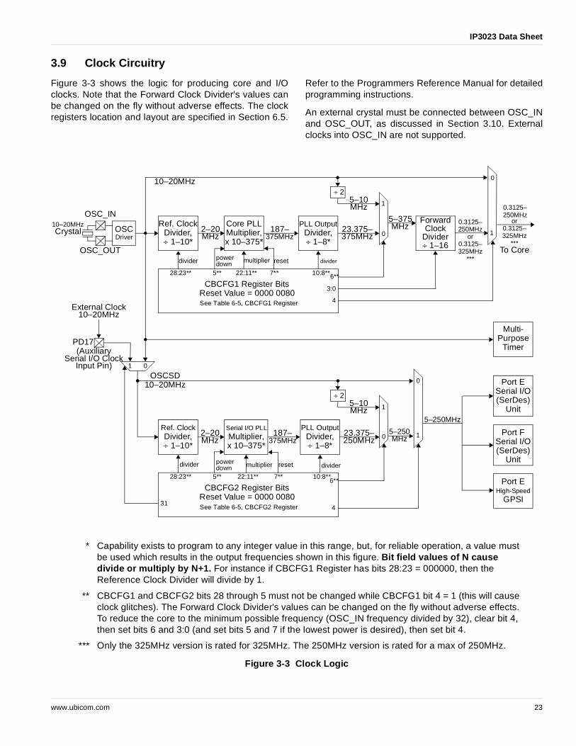
3.9 Clock Circuitry
Figure 3-3 shows the logic for producing core and I/Oclocks. Note that the Forward Clock Divider's values canbe changed on the fly without adverse effects. The clockregisters location and layout are specified in Section 6.5.
Refer to the Programmers Reference Manual for detailedprogramming instructions.
An external crystal must be connected between OSC_INand OSC_OUT, as discussed in Section 3.10. Externalclocks into OSC_IN are not supported.
* Capability exists to program to any integer value in this range, but, for reliable operation, a value must be used which results in the output frequencies shown in this figure. Bit field values of N cause divide or multiply by N+1. For instance if CBCFG1 Register has bits 28:23 = 000000, then the Reference Clock Divider will divide by 1.
** CBCFG1 and CBCFG2 bits 28 through 5 must not be changed while CBCFG1 bit 4 = 1 (this will cause clock glitches). The Forward Clock Divider's values can be changed on the fly without adverse effects. To reduce the core to the minimum possible frequency (OSC_IN frequency divided by 32), clear bit 4, then set bits 6 and 3:0 (and set bits 5 and 7 if the lowest power is desired), then set bit 4.
*** Only the 325MHz version is rated for 325MHz. The 250MHz version is rated for a max of 250MHz.
www.ubicom.com 23
IP3023 Data Sheet
3.10 Crystal Oscillator
Figure 3-4 shows the connections for attaching a crystalto the OSC oscillator. The crystal is connected across theOSC_IN and OSC_OUT pins. There is about 4pf ofcapacitance on each of OSC_IN and OSC_OUT pins toDVss. A parallel resonant crystal is recommended thathas a maximum ESR of 30 ohms at 20MHz, 60 ohms at10MHz. A feedback resistor (Rf) of 150K ohms must beconnected between OSC_IN and OSC_OUT for reliablecrystal startup.
The crystal manufacturer’s load capacitance rating (CL)should be equal to (C1 x C2) / (C1 + C2), where C1 =capacitance on OSC_IN (4pF + stray board capacitance +added capacitance), and C2 = capacitance on OSC_OUT(4pF + stray board capacitance + added capacitance).The trace length between the OSC pins and the crystalshould be as short as possible, to avoid noise coupling.
Figure 3-4 Crystal Connection
3.11 Clock Output Generator
The IP3023 provides two independently programmableclock output (CLK_OUT) signals on pins PB6 and PH13.The CLK_OUT signal is derived from the core clock by aclock divider circuit. The user can program the clockdivider by writing to a CLK_DIV[7:0] field. The core clockfrequency is divided by N+1, where N is the value in theCLK_DIV[7:0] field. To accomplish the division, an internalcounter samples CLK_DIV[7:0], then counts down to 0,then samples CLK_DIV[7:0] again, and so on. The stateof the counter (delayed by two core clock cycles) ispresented to the user in a PHASE[7:0] status field.
The CLK_OUT signal relates to PHASE[7:0] in themanner shown by the examples in Figure 3-5 (odd divisor)and Figure 3-6 (even divisor). For an odd divisor,CLK_OUT goes high when PHASE[7:0] reaches 0, andgoes low when PHASE[7:0] reaches (D+1)/2, where D isthe divisor. This produces a slightly asymmetricwaveform, as shown. For an even divisor, CLK_OUT goeshigh when PHASE[7:0] reaches 0, and goes low whenPHASE[7:0] reaches D/2. This produces a symmetricwaveform. If CLK_DIV[7:0] = 0, the output is constant low.
The value in CLK_DIV[7:0] can be changed at any time,without causing ill behavior, since the counter will alwaysfinish counting down to 0 before sampling CLK[7:0] again.The PHASE[7:0] status field allows the user to properlyalign a software process with the clock divider.
CLK_OUT is available on PB6 when Port B Function 1 isselected. CLK_DIV[7:0] is in bits [7:0] of the Port BSDRAM Function Control 2 register. PHASE[7:0] is in bits[15:8] of the Port B SDRAM Function Status 0 register. IfPB6 is used as an SDRAM Clock, CLK_DIV[7:0] shouldremain at a constant value of 3 (divide by 4).
CLK_OUT is available on PH13 when Port H Function 2is selected. CLK_DIV[7:0] is in bits [7:0] of the Port HClock Function Control 2 register. PHASE[7:0] is in bits[7:0] of the Port H Clock Function Status 0 register.
Figure 3-5 Clock Behavior when CLK_DIV[7:0] = 4 (divide by 5)
Figure 3-6 Clock Behavior when CLK_DIV[7:0] = 3 (divide by 4)
IP3KDS-025.eps
IP3000
OSC_IN OSC_OUT
C1 C2
Crystal
Rf = 150KΩ
1 0 4 3 2 1 0 34 2 1 0 4PHASE[7:0]
CLK_OUT
Core Clock
1 0 3 2 1 0 3 12 0 3 2 1PHASE[7:0]
CLK_OUT
Core Clock
24 www.ubicom.com
IP3023 Data Sheet
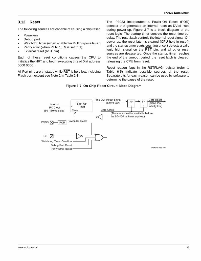
3.12 Reset
The following sources are capable of causing a chip reset:
• Power-on• Debug port• Watchdog timer (when enabled in Multipurpose timer)• Parity error (when PERR_EN is set to 1)• External reset (RST pin)
Each of these reset conditions causes the CPU toinitialize the HRT and begin executing thread 0 at address0000 0000.
All Port pins are tri-stated while RST is held low, includingFlash port, except see Note 2 in Table 2-3.
The IP3023 incorporates a Power-On Reset (POR)detector that generates an internal reset as DVdd risesduring power-up. Figure 3-7 is a block diagram of thereset logic. The startup timer controls the reset time-outdelay. The reset latch controls the internal reset signal. Onpower-up, the reset latch is cleared (CPU held in reset),and the startup timer starts counting once it detects a validlogic high signal on the RST pin, and all other resetsources are deasserted. Once the startup timer reachesthe end of the timeout period, the reset latch is cleared,releasing the CPU from reset.
Reset reason flags in the RSTFLAG register (refer toTable 6-5) indicate possible sources of the reset.Separate bits for each reason can be used by software todetermine the cause of the reset.
Figure 3-7 On-Chip Reset Circuit Block Diagram
Start-Up
Timer
Watchdog Timer Overflow
Internal
RC Clock
Time-Out Reset Signal
(active low)
RST
DVDD PORPower-On Reset
IP3KDS-023.eps
Clear(80–150ms delay)
Debug Port Reset
Core Clock
Core Reset
(active low,
initially low)
FF FF
Parity Error Reset
(This clock must be available before
the 80–150ms timer expires.)
www.ubicom.com 25
IP3023 Data Sheet
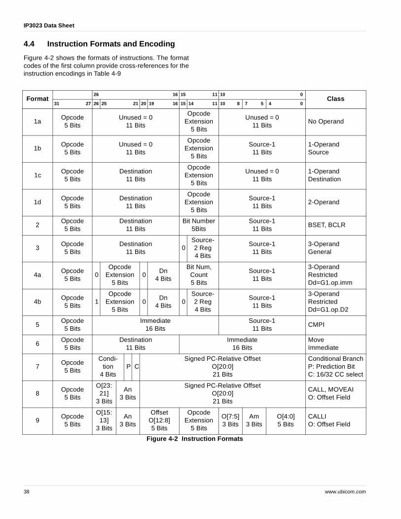
4.0 Instruction Set
4.1 Operand Addressing
The IP3023 has data types of three principle sizes: 8-bitbyte, 16-bit short word and 32-bit long word, as shown inFigure 4-1. There is also a 48-bit data type, used only foraccumulator results in the MAC register. The byteordering for operands in memory is big-endian, althoughbit numbering within registers is little-endian (as shown inFigure 4-1). Big-endian format means that the address ofthe operand refers to the byte address of the most-significant byte, and bytes are in memory in the order ofmost to least significant. For example, storing the 16-bitoperand 0x1234 at address 0x1000 means that 0x12 isstored at address 0x1000 and 0x34 is stored at address0x1001.
Both the program and data spaces are byte addressed,and operand addresses must be naturally aligned – thatis, they must be integer multiples of the operand size.Except for the IREAD instruction, if an operand address ismisaligned, execution does not halt, and some value forthe operand is returned, but the value returned in thatcase is not defined. If the misaligned address is a target,the target may or may not be modified, and additionalbytes near the target may be modified. When a referenceis made to a misaligned data space operand, as a sourceor target, the DCAPT interrupt bit is set, and the PC andthread number are captured. Unaligned addresses usedby IREAD accesses to program memory are not detected;the low-order two bits are ignored.
Figure 4-1 Big-Endian Data Formats of IP3023.
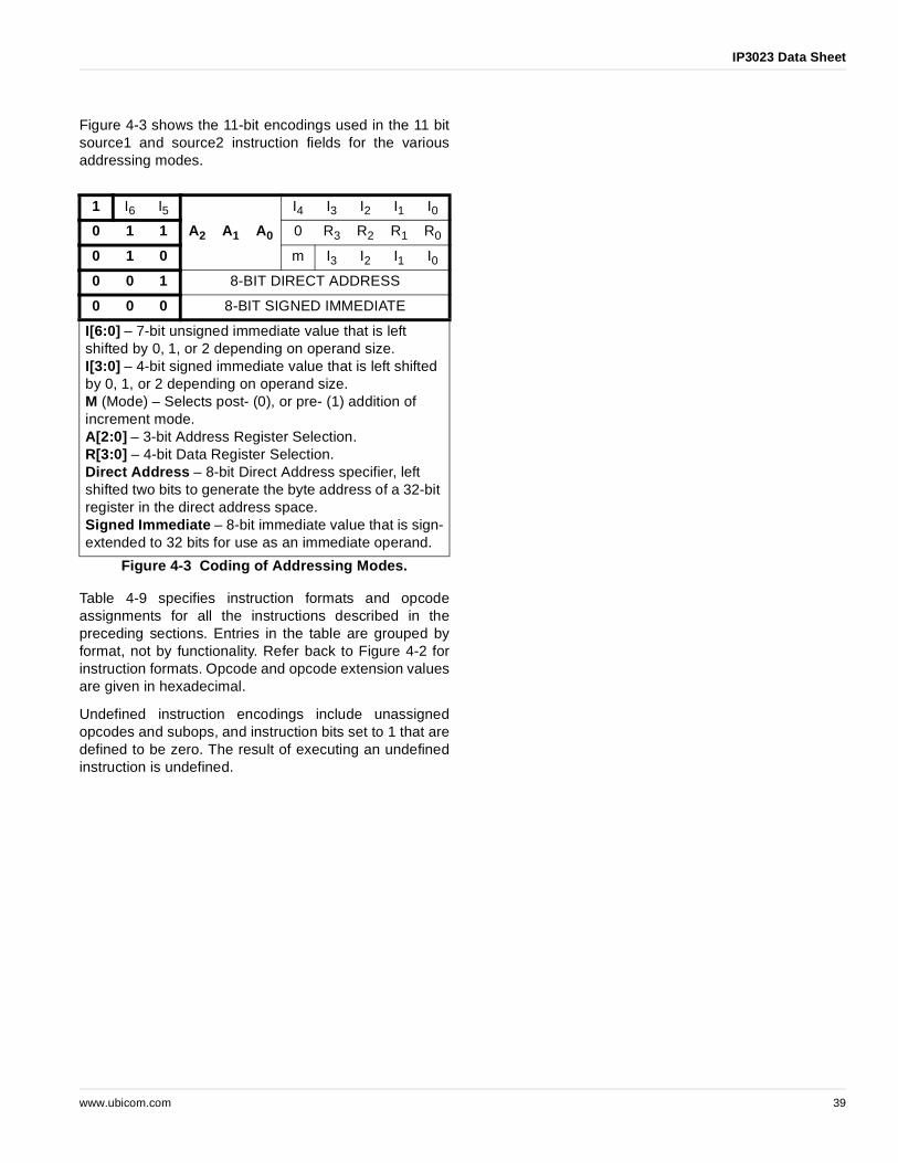
4.2 Addressing Modes
Most of the IP3023 instruction formats (as shown in Figure4-2) use a small number of common fields, which arealigned for ease of decoding. The most important of theseare the 11-bit source-1 and 11-bit destination operandspecifiers, and the 5-bit source-2 field. The latter maycontain either a 5-bit unsigned immediate value, or a dataregister number (in the right-most 4 bits), depending onthe specific instruction. A five-bit immediate value isnormally a bit number or a shift count, again depending onthe specific instruction.
The 11-bit source-1 and the 11-bit destination fields aredefined the same. This 11-bit field is used to select one ofthe following addressing modes (refer to Table 4-1 formore detail):
• Direct Addressing of the register address space• Register Indirect with 7-bit unsigned offset• Register Indirect with pre or post increment or
decrement• Register Indirect with indexing• Immediate: 8-bit value, sign extended to size of
operand type
An immediate value in the destination specifier is unusual,but it can be used to prevent write back of the instructionresult value to any real destination. The instruction is thenexecuted ‘for side effects only’ – i.e., setting the conditioncodes.
To encode all of the above in only 11-bits, variable lengthencoding is used. The minimum length encoding of a 1-bitis used for the register indirect with offset mode, allowingthe maximum number of bits for offset. This results in thefollowing two formats:
...where:
Details of this encoding scheme are shown in Figure 4-3.
SHORT WORD ADDRESS
LONG WORD ADDRESS
15 8 7 0
MS BYTE LS BYTE
MS BYTE LS BYTE
MS BYTE LS BYTE
MS BYTE
MS BYTE
MS BYTE
BYTE
BYTE
BYTE
BYTE
BYTE
BYTE
LS BYTE
LS BYTE
LS BYTE
INC
RE
AS
ING
AD
DR
ES
SE
S
31 0
0
0
2
4
4
8
IP3KDS-010.eps
24 23 16 `15 8 7
MS BYTE = MOST SIGNIFICANT BLS BYTE = LEAST SIGNIFICANT B
Register Indirect WithOffset: 1 i i A A A i i i i i
Other Addressing Modes: 0 x x A A A n n n n n
"i" : Indicates immediate value bits;
"A" : Indicates the three address bits that select one of the 8 address registers;
" x" and "n" : Other fields used by other addressing modes.
26 www.ubicom.com
IP3023 Data Sheet
In the Harvard architecture model, addressing modes fordata and program memory space have to be consideredseparately. For data address space, the supportedaddressing modes are described above. For programspace, both register indirect and PC relative addressingmodes are supported. Addressing modes for both spacesare summarized in Table 4-1.
4.2.1 The Register Address Space
Register addressing mode is used to address the general-purpose registers, D0-D15, as well as the addressregisters A0-A7, and all on-chip control registers. It is theonly mode that can access the core's control registers,because the address space in which these registersreside is not a subset of the general memory addressspace. A register in the register addressing space cannotbe accessed through a regular memory addressing modethat happens to resolve to the same numerical value.
The register addressing space is 256 registers in length,or 1024 bytes. The byte address specified in anassembler statement is right shifted two bits by theassembler, to generate the 8-bit register address offset.Although the assembler syntax requires a byte address,what is addressed in this mode is not bytes, but a spaceof 256 32-bit register locations. The register addressingspace covers access to the following registers:
• All Programmers' Model registers described inSection 3.1.
• On-chip control and status registers for overall chipand timer control.
Because the register addressing space is absolute, anassembler include file of EQU statements can be used todefine symbolic names for all the registers. Theninstructions can access these registers directly using theirsymbolic name as a source or destination operand.
www.ubicom.com 27
IP3023 Data Sheet
Table 4-1 Addressing Modes
Space Type ASM Syntax Effective Address (EA)
Operand Register $xx orRegister Mnemonic
No EA. Register address is 10 bits: (8-bit register number) || 00
Indirect (An) EA = An
Indirect with Offset
offset(An) EA = An + offset;PDEC only: EA = An - offset (in range 4 to 512);Assembly Syntax: Offset specified in bytes;Opcode Coding:Byte Operand: Offset = 7-bit unsigned immediate value;16-Bit Operand: Offset = 7-bit unsigned immediate value || 0;32-Bit Operand: Offset = 7-bit unsigned immediate value || 00;PDEC Operand: Offset = 11111111111111111111111 || 7 bit immediate || 00
Indirect with Post-Increment
(An)delta++ Step 1: EA = An ;Step 2: An ← An + deltaAssembly Syntax: delta specified in bytes;Opcode Coding:Byte Operand: delta = 4-bit signed immediate value;16-Bit Operand: delta = 4-bit signed immediate value || 0;32-Bit Operand: delta = 4-bit signed immediate value || 00.
Indirect with Pre-Increment
delta(An)++ Step 1: An ← An + deltaStep 2: EA = An ;Assembly Syntax: delta specified in bytes;Opcode Coding:Byte Operand: delta = 4-bit signed immediate value;16-Bit Operand: delta = 4-bit signed immediate value || 0;32-Bit Operand: delta = 4-bit signed immediate value || 00.
Indirect with Index
(An,Dn) EA = An + (Dn << log2(operand size in bytes))
Immediate #xxxx#xx
Operand is 16-bit or 8-bit immediate value taken from instruction. Value is sign-extended to 32-bits before use. For 8 bit immediate in general source-1, the EA is the 32-bit sign extended immediate.
CALLIInstruction
Indirect offset(An) PEA = An + (sign-extended coded offset <<2)Assembly Syntax: Offset is specified in bytes as a signed 18-bit number. This number is right shifted by two bits for instruction coding. Coded Offset = Assembly Offset[17:0] >> 2
CALLInstruction
Relative offset(PC) PEA = PC + (coded offset<<2)Assembly Syntax: Offset is specified in bytes as a signed 26-bit number. This number is right shifted by two bits for instruction coding. Coded Offset = Assembly Offset[25:0] >> 2
JMPccInstruction
Relative offset(PC) PEA = PC + (Opcode Offset)<<2Assembly Syntax: Offset is specified in bytes as a signed 23-bit number. This number is right shifted by two bits for instruction coding. Opcode Offset = Assembly Offset[23:0] >> 2
Notation: EA: Data Effective Address; PEA: Program Space Effective Address
28 www.ubicom.com
IP3023 Data Sheet
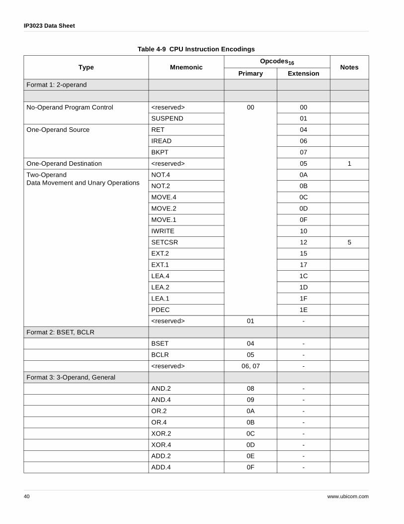
4.3 Instruction Set Summary
The instruction set has a fixed-length 32-bit instructionword, and the internal data path is 32 bits wide.
The CSR register (refer to Section 6.2.1 on page 91)contains two sets of condition codes: 16-bit conditioncodes and 32-bit condition codes. Both sets of conditioncodes are calculated for the results of arithmetic andlogical instructions all the time. The programmer choosesthe appropriate set for conditional jump instructions. Thebits of both sets of codes have the same symbols, whichare defined in Table 4-2.
The following points apply to all instructions, in theinstruction description tables that follow:
• The ".size" field in instruction syntax refers to the datamemory width of operands, and not the instructionwidth or the ALU result width; both the latter arealways 32-bits.
• With arithmetic, logical, and shift operations, if thesource is 16-bits, it is always sign extended to 32-bitsbefore the operation to match the width of the internaldata path. Only MOVE.1 and MOVE.2 zero-extend asmaller source operand, when the destination is a 32-bit register (i.e., any register in the register addressspace – most frequently a data register). The 16-bitcondition codes allow operation with 16-bit unsignedintegers in memory.
• All arithmetic and logical operations are performed in32-bit resolution. If the destination is in memory and
the instruction's operand size is only 16 bits, it is thelower 16 bits of the 32-bit result that is written tomemory.
• The source-2 operand, for instructions with more thanone input operand, is always either a 32-bit dataregister, or (in the case of shift and bit fieldinstructions) a 5-bit zero-extended immediate value.
• Data registers, address registers, and other registersin the register address space, used as source ordestination operands, are always 32-bits wide.
• An immediate 8-bit value in the source-1 operandspecifier is always sign-extended to 32-bits beforeuse.
• The tables indicate which condition flags are set byeach instruction. In general, any instruction whichcomputes a 32-bit result will set both the N and Z flagbits. Only instructions that can generate a carry oroverflow will set the C or V bits. BTST, BSET, andBCLR set only the Z bit. MOVE instructions do notaffect the flags.
• The indicated condition flag bits are always setindependently in both the 16- and 32-bit conditioncodes. Thus, if a 32-bit result were all 0's in the lower16 bits, but had some non-zero bits in the upper 16bits, the 16-bit condition result would be '1' in the Z bitand '0' in the N bit. The 32-bit result would be '0' in theZ bit and a copy of bit 31 in the N bit.
Example: As the following two instructions demonstrate,the size refers to data memory access size. The arithmeticand logical operations are always performed at 32-bitresolution.
4.3.1 Arithmetic and Logical Operations
Integer arithmetic support consists of the basic operationsof add, subtract, multiply, and multiply-accumulate (MAC).Logical operations include the four basic operations ofAND, OR, XOR, and NOT. They perform bit-wise Booleanoperations on operands.
The following paragraphs discuss selected instructions inmore detail.
ADDC and SUBC
ADDC and SUBC use the C-bit in the 32-bit conditioncode to implement extended precision arithmeticoperations. The C-bit is used for any carry and borrowbetween different 32-bit words of an extended operand
Table 4-2 16-Bit and 32-Bit Condition Codes
Symbol Description
N Negative. Set if result is negative, cleared otherwise.
Z Zero. Set if result is zero, cleared otherwise. For ADDC and SUBC the Z bit is cleared if the result is nonzero, and left unchanged if the result is zero. This bit does not include any testing of the carry bit.
V Overflow. For arithmetic operations where overflow is a meaningful possibility, the V bit is set if overflow occurs, and cleared if it does not. For other operations, the bit remains unchanged from its value before the operations.
C Carry. For arithmetic operations where a carry out is a meaningful possibility (add, subtract, and compare), the C bit is set to the value of the carry out. For subtract and compare operations the C bit contains the complement of the borrow.
(there is no ADDC.2 or SUBC.2). For SUBC, thecomplement of the C-bit on input is the “borrow” value forthe operation. The borrow is effectively added to the right-hand operand (the subtrahend) before it is subtractedfrom the left hand operand. (In practice, what that meansis that, whereas normal subtraction is implemented byadding the logical complement of the right hand operandto the left hand operand, with a forced '1' as carry in,SUBC uses the input value of the C-bit as the carry in.)
The Z bits are treated differently for ADDC and SUBCthan for other instructions. If the result is nonzero, the Zbit is cleared, but if the result is zero, the Z bit is notchanged. When adding multiprecision numbers, first anADD instruction will set or clear the Z bit for the leastsignificant 32 bits. Subsequent ADDC instructions canonly clear the Z bit. After the sequence of ADD andADDC, the Z bit will be set if the multiprecision result iszero.
There is limited scope for inserting instructions betweenthe instruction that sets the carry flag value and the ADDCor SUBC instruction intended to use it. MOVE, and otherinstructions that don't affect the C flag are safe, but loopend tests are problematic. A loop end test will normallyaffect the flag value. Therefore, it is desirable to use in-lineexpansions, rather than loops, for extended precisionarithmetic. Since the normal IP3023 arithmetic operationsare 32 bits wide, it only takes a single ADD, followed byone ADDC, to perform a 64-bit extended precision add.
In rare cases, where very long extended precisionoperations must be implemented, it is possible to use theLEA instruction to decrement a loop counter register, anduse an EXT instruction to set the Z and N bits of thecondition codes, without affecting the C and V flags. Thatpermits a conditional branch on non-zero for the loop endtest, at the cost of the extra EXT.
MULF and MAC
These perform multiply and multiply-accumulate functionson 16-bit fixed point, or so-called “fractional” data types(S.15), most commonly used by Digital Signal Processingalgorithms. MULF generates a 32-bit number in the S.31format, and stores it to the 48 least significant bits of theMAC accumulator register, sign-extending the 32-bitresult to 48 bits. The upper 16 bits of MAC_HI are clearedby MAC and MULF. MAC performs an implicit MULFoperation, and adds the 32-bit result to the 48-bitaccumulator value. The format of the accumulator isS16.31. Source-2 can be a Dn register or a 5-bitimmediate representing a number in the range 0 to31*2–15.
MULS and MULU
These perform multiply functions on signed or unsigned16 bit integers. The result is sign extended or zeroextended to 48 bits and stored into MAC_HI andMAC_LO. The upper 16 bits of MAC_HI are cleared.Source-2 can be a Dn register or a 5-bit unsignedimmediate.
MAC_RC16
The MAC_RC16 register is set by any instruction thatimplicitly targets MAC_HI and MAC_LO. It is not modifiedby an instruction that explicitly targets those registers.The result being placed in MAC_HI/MAC_LO isconsidered to be a number in S16.31 format. This is atwo's complement 48 bit fractional number with 31 bitsafter the decimal point. This number is first rounded tohave 15 bits after the decimal point. To round, the valueof the 16th bit after the decimal point is added to the 15thbit after the decimal. After rounding, the result is clampedto be in the range 0.111111111111111 (binary) to1.000000000000000 (binary). The sign of the clampedvalue is the same as the sign of the original number,before rounding, to prevent the highest positive numberfrom being rounded to the lowest negative number. Afterrounding and clamping, the result is sign extended to 32bits and stored in the MAC_RC16 register. The resultingformat has 17 copies of the sign bit, a decimal point, and15 fractional bits, in two's complement.
CRCGEN
This is a special purpose instruction for efficientcalculation of CRC values in message protocols, such asEthernet, and bit-stream scrambling. It models theoperation of a Linear Feedback Shift Register (LFSR), forany generating polynomial of order 32 or less. Itprocesses eight bits of input at a time. It is defined asfollows:
30 www.ubicom.com
IP3023 Data Sheet
Syntax: CRCGEN s1, s2
Inputs: s1 – next data byte, B (general source, typically from memory)
s2 – generating polynomial, P (Dn register or 5 bit immediate)
MAC_LO – current CRC value, C
Outputs: MAC_LO – new CRC value, C'
MAC_HI – scrambled output byte, S, shifted into the most significant byte
MAC_RC16 - S16.15 image of MAC-HI, MAC_LO
Operation:
X = (C ^ B) & 0xFF;
F = X;
for (i=0; i<8; i++) F = (F>>1)^(F&1 ? P : 0);
S = C & 0xFF;
MAC_LO = F ^ (C >> 8);
MAC_HI = (MAC_HI >> 8) | (S << 24);
MAC_RC16 ← S16.15(MAC_HI, MAC_LO)
Table 4-3 Arithmetic and Logical Instructions
Mnemonic & Oper-ands Description
Flags (for both 16-bit and 32- bit operands)
Operand Size
(Bytes)
ADD.2 d,s1,s2ADD.4 d,s1,s2
16/32-Bit Add Operation:d ← s1 + s2
C,Z,N,V 2, 4
ADDC d,s1,s2 32-Bit Add with Carry:d ← s1 + s2 + C(32-bit C Flag)
C,Z,N,V 4
AND.[2/4] d,s1,s2 d ← s1 AND s2 N,Z 2, 4
CMPI s1,#imm16 16-Bit Compare with Immediate Value:s1 – (sign-extended #16-bits)
C,Z,N,V 2
CRCGEN s1,s2CRCGEN s1,#POLY
32-bit incremental CRC Generation Instruction:MAC_LO holds current CRC;s1 specifies the next input bytes2 specifies the generating polynomialMAC_LO ← CRC(MAC_LO, s1, s2)MAC_HI[23:0]← MAC_HI[31:8]MAC_HI[31:24]← scrambled output byteMAC_RC16 ← S16.15(MAC_HI, MAC_LO)
1
LEA.1 d,s1LEA.2 d,s1LEA.4 d,s1
Load Effective Address: d ← EA(s1);
Calculates the effective-address for the referenced data operand, and stores the address into destination. S1 must not be Register addressing mode.The destination size is always 32 bits. If the destination is an An register (and the Destination Thread Select bit in the CSR is not set), a fast path eliminates hazards with a later An use.
- 1, 2, 4 (Source)
www.ubicom.com 31
IP3023 Data Sheet
PDEC d,s1 d ← EA(s1);Identical to LEA.4, except that the 7-bit offset in base+offset addressing mode is extended to 32 bits by adding 23 1-bits (11111111111111111111111 || 7-bit immediate || 00).
4
MAC s1, s2MAC s1, #imm
The Dn field is coded as zero16 x 16-bit signed Fractional Multiply-Accumulate:
SUBC d,s1,s2 32-Bit Subtract with Carry:d ← s1 – s2 – !C (32-bit C Flag)
where: C = 1 if there is no borrow.
C,Z,N,V 4
XOR.[2/4] d,s1,s2 d ← s1 XOR s2 N,Z 2, 4
Notes:·Fractional multiply has an implicit left-shift by one; otherwise, it would end up with two sign bits.·SE48: Indicates sign-extension to 48 bits.·S16.15: The 48-bit accumulator value is rounded, with saturation, to a 16-bit fractional value (S.15 format), then sign-extended to 32 bits (S16.15 format).
Table 4-3 Arithmetic and Logical Instructions
Mnemonic & Oper-ands Description
Flags (for both 16-bit and 32- bit operands)
Operand Size
(Bytes)
32 www.ubicom.com
IP3023 Data Sheet
4.3.2 Shift and Bit-Field OperationsTable 4-4 Shift and Bit-Field Instructions
If 's1' is a 16-bit operand, it is sign-extended to 32 bits before the operation; 'd' must be a data register.
N, Z
BFEXTU d, s1, s2BFEXTU d, s1, #cnt
Bit Field Extract. Extracts a bit-field from 32-bit s1 operand and places it into LSBs of destination. s2 (Dn or 0-extended 5-bit immediate) contains the parameters:
Bits 4:0: Bit-Field Length;Bits 12:8: Bit-Field Start position (low order bit);
The result is zero-extended to 32 bits. The destination must be a data register. If Length == 0, then result = 0;If start + length ≥ 32 → Then, cut at the left edge.
N, Z
BFRVRS d, s1, s2BFRVRS d, s1, #cnt
Bit Field Reverse. Reverse bit ordering 32-bit s1 operand, followed by logical right shift by shift count:
d ← (Reverse(s1)) >> s2[4:0]d ← (Reverse(s1)) >> cnt
If 's1' is a 16-bit operand it is sign-extended to 32 bits before the operation; 'd' must be a data register.
N, Z
MERGE d, s1, s2MERGE d, s1, #imm
Bitwise Merge. This is a 32-bit merge that operates as follows:d ← (s1 & msk) | (s2 & !msk);d ← (s1 & msk) | (imm & !msk);
'msk' is a 32-bit selection control mask, read from the SOURCE3 register. 's1' is a 32-bit operand. The second source operand may be either a data register or a 5-bit immediate value, zero-extended to 32 bits. 'd' must be a data register
's1' is a 16-bit operand; the second operand is a data register or 5-bit immediate. 'd' must be a data register
N, Z
Notes: · "||" designates concatenation of bits.·"Xn": designates 'n' repetitions of bit 'X'.·"|" Indicates logical OR operation; "&" indicates logical AND operation; "!" indicates logical negation.·">> N" indicates right shift by N bits.
Table 4-4 Shift and Bit-Field Instructions
Mnemonic & Operands Description Flags
Table 4-5 Single Bit Operations
Mnemonic & Operands Description Flags
BTST s1, s2BTST s1, #bit_number
Bit Test. Test the bit indicated by the # bit_number field, of the 32-bit s1 operand and set the Z bits accordingly. The bit may be specified by the contents of the s2 D-register, or by a 5-bit immediate value.
Z ← !s1[bit]
Z
BSET d, s1, #bit_number Bit Set.Step 1: Test the bit in s1 indicated by the #bit_number field and set Z bits accordingly (Z ← !bit).Step 2: Set the selected bit in d.
Z
BCLR d, s1, #bit_number Bit Clear.Step 1: Test the bit in s1 indicated by the #bit_number field and set Z bits accordingly (Z ← !bit).Step 2: Clear the selected bit in d.
Z
Notes:1. BSET and BCLR: source and destination operands are typically the same, but this is not required.
34 www.ubicom.com
IP3023 Data Sheet
4.3.4 Data Movement And Extension Instructions
Table 4-6 Data Movement And Extension Instructions
Mnemonic & Operands Description Flags
MOVEI d,#imm16 Move 16-Bit Immediate Value:if (destination is a directly addressed register)then
Destination ← SE32(imm16);else
Destination ← imm16; ( 2 byte destination size)
-
MOVEAI a,#imm24 Move 24-bit Immediate Value into bits [30:7] of the target address register. Bits 31 and [6:0] are cleared
-
EXT.1 d,s1 Sign-Extend byte from source to 32-bits and store result to destination. d ← s1[7]24 || s1[7:0]
The sign extension is effective only if the destination is a register. If it is a memory destination, the destination size, being the same as the source size, makes the operation equivalent to MOVE.1. If the source is a direct register, 8 bits is extracted from that register and sign-extended.
N,Z
EXT.2 d,s1 Sign-Extend 16 bit source-1 operand to 32-bits and store result to destination.
d ← s1[15]16 || s1[15:0]The sign extension is effective only if the destination is a register. If it is a memory destination, the destination size, being the same as the source size, makes the operation equivalent to MOVE.2. If the source is a direct register, 16 bits is extracted from that register and sign-extended.
N,Z
SETCSR s1 32-Bit Move: CSR of current context ← s1
This is used to switch context back, since changing the destination context field of CSR is otherwise not possible to undo.
-
MOVE.1 d,s1 8-Bit Move: d ← s1
If the destination is a directly addressed register, then the upper 24 bits (31:8) are cleared to zero.
-
MOVE.2 d,s1 16-Bit Move: d ← s1
If the destination is a directly addressed register, then the upper 16 bits (31:16) are cleared to zero.Both source and destination addresses must be two-byte aligned – i.e., the least significant bit of address must be zero. Otherwise, result is architecturally undefined.
-
MOVE.4 d,s1 32-Bit Move: d ← s1
Moves a long word from source to destination.Both source and destination address must be quad-byte aligned – i.e., the two least significant bits of address must be zero. Otherwise, result is architecturally undefined.
-
Notes:·SE32: Indicates sign extension to 32 bits.
www.ubicom.com 35
IP3023 Data Sheet
4.3.5 Program Control Instructions
Table 4-7 Program Control Instructions
Mnemonic & Operands Description Flags
JMP<cc>.C.T/F offset PC-Relative Conditional Jump:If specified condition function evaluates to '1' (True), then: PC ← PC + signed 23-bit offset; else: PC ← PC + 4.
Branch prediction: T: Take branch (1); F: Continue (0).C: Condition Code Set Select:
C = S : Select 16-bit Condition Codes (0);C = W : Select 32-bit Condition Codes (1).
Offset is two's complement 23 bits in assembly syntax, of which only the most significant 21 bits are used in the instruction. The processor shifts this 21-bit offset value left by two bits before using it.
None
CALL An, offset PC-Relative Call To a Subroutine:Step 1: An ← PC+4Step 2: PC ← PC + Signed OffsetOffset is two's complement 26 bits in assembly syntax, of which only the most significant 24 bits are used for the opcode. The processor shifts this 24-bit offset value left by two bits before using it. The return address is saved into the An register selected.
None
CALLI An, offset(Am) Address Indirect Call To a Subroutine:Step 1: Target ← Am + Signed 18-bit OffsetStep 2: An ← PC+4Step 3: PC ← TargetOffset is two's complement 18 bits in assembly syntax, of which only the most significant 16 bits are used for the opcode. The processor shifts this 16-bit offset value left by two bits before using it. The return address is saved into the An register selected.
None
RET s1 Return from subroutine:s1 → PC
None
SUSPEND Suspends the current thread until an interrupt condition for that thread occurs.
PC ← Address of next instructionMT_ACTIVE[thread] ← 0
None
BKPT s1 Breakpoint Instruction. The source operand is a bit mask that indicates which additional contexts to suspend. The bit number of a bit set in the mask is the thread number that is to be suspended. The thread that executes the BKPT instruction is always suspended.PC ← Address of BKPT instructionMT_DBG_ACTIVE[thread] ← 0For each thread specified by s1,
IWRITE pea_d, s1 (pea_d) ← s1Writes the 32-bit source operand to pea address.
None
IREAD pea_s1 IREAD Register ← (pea_s1)Reads a shadow SRAM or flash program memory location into the issuing thread's IREAD_DATA register. The operand is always 32-bits wide.
None
Restriction: The destination (pea_d) and source (pea_s1) address modes are restricted to be one of the based (indirect) address modes – i.e., they are defined as:pea_d, pea_s1 = (An), or offset(An), or delta(An)++, (An)delta++, or (An, Dm)
Notes: None of these program space instructions is blocking, i.e., they all take single-clock cycle to execute. The MEM BUSY bit in the context specific ROSR register indicates the completion of the operation. It is the program's responsibility not to initiate another of these instructions before the previously issued one completes.
www.ubicom.com 37
IP3023 Data Sheet
4.4 Instruction Formats and Encoding
Figure 4-2 shows the formats of instructions. The formatcodes of the first column provide cross-references for theinstruction encodings in Table 4-9
Conditional BranchP: Prediction BitC: 16/32 CC select
8Opcode5 Bits
O[23:21]
3 Bits
An3 Bits
Signed PC-Relative OffsetO[20:0]21 Bits
CALL, MOVEAIO: Offset Field
9Opcode5 Bits
O[15:13]
3 Bits
An3 Bits
OffsetO[12:8]5 Bits
Opcode Extension
5 Bits
O[7:5]3 Bits
Am3 Bits
O[4:0]5 Bits
CALLIO: Offset Field
38 www.ubicom.com
IP3023 Data Sheet
Figure 4-3 shows the 11-bit encodings used in the 11 bitsource1 and source2 instruction fields for the variousaddressing modes.
Figure 4-3 Coding of Addressing Modes.
Table 4-9 specifies instruction formats and opcodeassignments for all the instructions described in thepreceding sections. Entries in the table are grouped byformat, not by functionality. Refer back to Figure 4-2 forinstruction formats. Opcode and opcode extension valuesare given in hexadecimal.
Undefined instruction encodings include unassignedopcodes and subops, and instruction bits set to 1 that aredefined to be zero. The result of executing an undefinedinstruction is undefined.
1 I6 I5 I4 I3 I2 I1 I0
0 1 1 A2 A1 A0 0 R3 R2 R1 R0
0 1 0 m I3 I2 I1 I0
0 0 1 8-BIT DIRECT ADDRESS
0 0 0 8-BIT SIGNED IMMEDIATE
I[6:0] – 7-bit unsigned immediate value that is left shifted by 0, 1, or 2 depending on operand size.I[3:0] – 4-bit signed immediate value that is left shifted by 0, 1, or 2 depending on operand size.M (Mode) – Selects post- (0), or pre- (1) addition of increment mode.A[2:0] – 3-bit Address Register Selection.R[3:0] – 4-bit Data Register Selection.Direct Address – 8-bit Direct Address specifier, left shifted two bits to generate the byte address of a 32-bit register in the direct address space.Signed Immediate – 8-bit immediate value that is sign-extended to 32 bits for use as an immediate operand.
www.ubicom.com 39
IP3023 Data Sheet
Table 4-9 CPU Instruction Encodings
Type MnemonicOpcodes16
NotesPrimary Extension
Format 1: 2-operand
No-Operand Program Control <reserved> 00 00
SUSPEND 01
One-Operand Source RET 04
IREAD 06
BKPT 07
One-Operand Destination <reserved> 05 1
Two-OperandData Movement and Unary Operations
NOT.4 0A
NOT.2 0B
MOVE.4 0C
MOVE.2 0D
MOVE.1 0F
IWRITE 10
SETCSR 12 5
EXT.2 15
EXT.1 17
LEA.4 1C
LEA.2 1D
LEA.1 1F
PDEC 1E
<reserved> 01 -
Format 2: BSET, BCLR
BSET 04 -
BCLR 05 -
<reserved> 06, 07 -
Format 3: 3-Operand, General
AND.2 08 -
AND.4 09 -
OR.2 0A -
OR.4 0B -
XOR.2 0C -
XOR.4 0D -
ADD.2 0E -
ADD.4 0F -
40 www.ubicom.com
IP3023 Data Sheet
ADDC 10 -
SUB.2 11 -
SUB.4 12 -
SUBC 13 -
<reserved> 14-17 -
Format 4: 3-Operand, Restricted
MULS 02 01 2
MULU 03 2
MULF 05 2
BTST 06 3
CRCGEN 08 2
MAC 09 2
LSL.4 10
LSL.2 11
LSR.4 12
LSR.2 13
ASR.4 14
ASR.2 15
BFEXTU 16
BFRVRS 18
SHFTD 1A
MERGE 1C
SHMRG.2 1E
SHMRG.1 1F
<reserved> 03 -
Format 5: Compare Immediate
CMPI 18 - 3
Format 6: Move Immediate
MOVEI 19 - 4
Format 7: Conditional Branch
JMP<cc> 1A -
Format 8: CALL, MOVEAI
CALL 1B -
MOVEAI 1C -
Table 4-9 CPU Instruction Encodings
Type MnemonicOpcodes16
NotesPrimary Extension
www.ubicom.com 41
IP3023 Data Sheet
<reserved> 1D -
Format 9: Call Indirect
CALLI 1E -
<reserved> 1F -
1. Dest operand must be a memory address mode (not immediate or register).2. Destination is implicit MAC_HI, MAC_LO, MAC_RC16 registers.
Destination field in instruction is coded as zero.3. Destination is implicit CSR register (CCs).4. If destination is data memory address, operand size is 16 bits.5. Destination is coded with the direct register address of the CSR register.
Table 4-9 CPU Instruction Encodings
Type MnemonicOpcodes16
NotesPrimary Extension
42 www.ubicom.com
IP3023 Data Sheet
5.0 Peripherals
5.1 Overview
The IP3023 supports a number of I/O ports, each of whichcan be configured as general purpose I/O or assigned toa specific function. The available hardware functionsinclude support and control functions, such as clockgeneration and interrupts, as well as functions for allowingconnections to specific on-chip I/O controller/acceleratorunits. Table 5-1 summarizes the functions available ateach port.
5.2 Shared Port Architecture
All ports share a common base architecture. Dependingon the specific requirements of the port, each port can becomposed of :
• A register set to control and monitor the portfunctions.
• Data FIFOs for efficient movement of transmit andreceive data.
• One or more independently operating function blocks.
• Muxes that control function selection.
All ports share these common features:
• Configurable (except port A) to operate as GPIO only.
• FIFO interface for data, independent of protocol.Alignment and packing of data within the 32-bit FIFOword is function specific. FIFOs are up to 128 byteslarge; the actual size is port specific.
• External clock sources available.
5.2.1 Port Registers
Port registers are used for function selection, settingfunction parameters, function control, and reportingfunction and port status. Port specific register definitionsare provided in Section 6.6 and following sections.
5.2.2 Interrupts
Each port has four registers that participate in interruptcontrol for that port:
• Interrupt Status Register
• Interrupt Mask Register
• Interrupt Set Register
• Interrupt Clear Register
These are 32-bit registers, but only bits [15:0] arededicated to interrupt control. Bits 15:0 correspond by bitposition to each of 16 potential interrupt sources.
For each port, there are three bits in the global interruptregister INT_STAT1[23:0] and in each of the per-threadinterrupt mask registers INT_MASK1[23:0]. The threeinterrupt bits correspond to port interrupt conditions asfollows:
• Interrupt 0 – Receive FIFO high watermark condition.
• Interrupt 2 – All other port interrupt conditions.
5.2.3 FIFO Management
The FIFOs are initialized by asserting one of the set bitsTX FIFO Reset or RX FIFO Reset.
The TX Underflow and RX Overflow Interrupts areprovided to inform software of attempts to transmit whenthe transmit FIFO is empty or to receive when the receiveFIFO is full.
Table 5-1 I/O Port Functions
Port Function
A& B
Provide support for external instruction memory as well as some slave peripheral devices. To provide good performance, processor instruction fetches to flash and SDRAM accesses are controlled by hardware state machines. Accesses to all other devices attached to these ports are performed through direct manipulation of the I/O pins.
C Provides hardware support for MII.
D Provides a second MII port.
E Provides ½ of a third MII port as well as SerDes hardware functionality. This SerDes block does not support 10Base-T, because the chip itself implements only one receiver, which is associated with Port F. Also provides a high-speed GPSI port.
F Provides the other half of the MII (Port E also supporting half) and SerDes hardware functionality. This SerDes supports 10Base-T.
G Entirely GPIO with no additional hardware I/O acceleration.
H Provides a fourth MII port as well as GPIO and hardware clock generation support for peripheral timing.
www.ubicom.com 43
IP3023 Data Sheet
At any time, software can determine how full the transmitand receive FIFOs are by examining theTX_FIFO_DEPTH and RX_FIFO_DEPTH registers.
To help avoid overflow or underflow conditions, theconcept of FIFO watermarks is implemented. Softwareuses control registers to set the TX FIFO Low Watermarklevel and RX FIFO High Watermark level. Hardware usesthe RX FIFO High Watermark interrupt or TX FIFO LowWatermark interrupt to inform software when a watermarklevel has been reached.
If a transmit FIFO Watermark Interrupt, or a receive FIFOWatermark Interrupt has occurred, and the appropriateaction has not been taken to address the interrupt (i.e., fillthe transmit FIFO or empty the receive FIFO) the interruptwill persist against any attempt by software to clear theinterrupt. (The mask bit must be set to cause an interrupt.)
A second receive FIFO is installed in those I/O ports thathave a function needing a second FIFO (see Table 5-2).Where only one receive FIFO is installed in an I/O port,the receive FIFO is installed as FIFO 0.
Access to a specific receive FIFO is controlled through theReceive FIFO Select bit (Function Select[3]). Setting thisbit to 0 causes all accesses to the receive FIFO (reset,status, data) to reference receive FIFO 0. Setting this bitto 1 causes receive FIFO accesses to reference receiveFIFO 1.
An interrupt that was set due to the action of one FIFO willremain set after the Receive FIFO Select bit is changed toselect the other FIFO, even if the newly selected FIFO isnot asserting this interrupt. If a FIFO is filled beyond thelevel set by the watermark trigger level and that FIFO isnot currently selected, an interrupt will not be asserteduntil that FIFO has been selected through the ReceiveFIFO Select bit. The following register fields are affectedby Receive FIFO Select bit:
When a receive FIFO overflows or a transmit FIFOunderflows, all other FIFO status information is undefined,and software must reset the FIFO.
H 16 yes yes 64 Byte 64 Byte GPIO MII * GPIO, Clock
N/A
* A second FIFO is available at these ports.
44 www.ubicom.com
IP3023 Data Sheet
5.3 External Flash Controller
This controller manages the interface between the IP3023and an the external flash device. The controller canrespond to the IREAD instruction of the processor. Thecontroller can also respond to a more general registerinterface on Port A and Port B.
This controller is compatible with any 8-bit flash devicethat has a JEDEC standard non-multiplexed address pathof 22-bits and which is controlled by the CE, OE, and WEpins. This includes the following devices:
Table 5-3 shows the signals and pins that interface withthe external flash device.
The flash device is physically controlled by sendingexternal bus commands which are combinations of theFCE, OE, and WE signals; those supported by thiscontroller are shown in Table 5-4. This list is common toall flash types supported by this controller. These externalbus commands are generated automatically by the flashcontroller in response to IREAD instructions or to usercommands that have been sent to it.
The default state is for the controller to hold the flashdevice in standby mode. This allows the same pins onIP3023 to be shared safely with the SDRAM controller orother functions on the same port.
5.3.1 Processor IREAD Interface
The controller responds to the IREAD instruction of theprocessor, returning a word from the desired address.
The IREAD instruction is handled only when this port’sFUNC_SEL is set to the flash function (the default power-up condition). If another function on the same port isselected later, the flash controller is disabledautomatically (FCE is deactivated). This means that theIP3023 can boot by performing the initial fetches fromflash without having to explicitly enable this port function.It also means that, to copy data from the flash to theSDRAM (which share the same physical pins), softwaremust alternate between enabling these two functions onthe port.
When disabled (Port B flash function not selected), thecontroller completely ignores all IREAD instructions, anddoes not send any response; instead it asserts an errorinterrupt and enters an error state, where it remains untilfunction reset. The error condition should be clearedbefore applying the function reset; otherwise, thecontroller simply re-enters the error state.
IREAD instructions cause the flash controller toautomatically send four successive read bus commandseach returning a byte to an internal buffer. These bytesare combined together to form a full 32-bit word that isreturned to the processor core.
The read/write access timing parameter (XFL_TAVAV)defaults to 64 CORE_CLK cycles to guarantee that anydevice rated faster than 150ns can be supported on futureIP3000 products rated up to a maximum frequency of400MHz. This parameter is configurable to lower valuesto speed up the flash interface.
The number of cycles required to complete an instructionfetch can be calculated using the formula: cycles =4*(XFL_TWAIT + XFL_TAVAV) + 6 + PIPE_DELAY.Unfortunately, the value of PIPE_DELAY cannot be
Table 5-3 External Flash Signal Summary
Flash Signal Pin Direc-
tion Description
ADDR [21:0]
PA[21:0]
O Byte address on the external flash device.
OE PA22 O Output enable.
WE PA23 O Write enable.
DATA [7:0]
PA[31:24]
I/O Input and output data.
FCE PB7 O Flash Chip Enable. Connected to flash device’s CE pin. It is active only when the flash function for Port A is enabled. This pin should be tied to a pullup resistor, so that the flash chip isn’t enabled while the IP3023 is in reset.
Table 5-4 Supported Flash Bus Commands
Command FCE OE WE A[21:0] DQ[7:0]
Standby H -- -- -- --
Output Disabled
L H H -- --
Read L L H Address Data In
Write L H L Command or Address
Command or Data Out
Illegal L L L -- --
www.ubicom.com 45
IP3023 Data Sheet
specified, since it depends on the scheduling tableconfigured by software. For 100% scheduling of therequesting thread, the value would be six.
If software disables the controller (by deassertingFUNC_SEL) while an IREAD operation is in progress,then the flash controller enters ERROR state. Becausethe operation has not completed, there is never anyacknowledgement sent back to the processor core.Without this signal, the MEM_BUSY bit in the thread-specific ROSR register cannot be cleared. The only wayto exit the ERROR state is to reset the controller. Byensuring that FUNC_SEL is reasserted before applyingreset to the controller, the original IREAD operation will berestarted.
If an IREAD is interrupted by software asserting XFL_ENin preparation for an XFL-style operation, then the flashcontroller can perform internal arbitration. It allows theIREAD to complete successfully before switching over tohandle XFL-style user commands. Any XFL_STARTpulse sent during this period when the IREAD iscompleting will be ignored. Once the flash controllerenters the XFL-mode, it ignores subsequent IREADrequests until XFL_EN is deasserted.
5.3.2 Port Register Interface
The IWRITE instruction is not directly supported by thiscontroller. Instead, a port interface is provided that isconnected just like any other I/O function, with usercommands, data FIFOs, and register parameters. Table5-5 lists the user commands that are available throughdirect port access.
Table 5-6 shows the register fields through which softwareprograms the flash controller.
Table 5-5 Supported User Commands
CMD Code
UserCommand Function
11 XFL_NOP Does nothing. Sends "output disabled" bus command.
01 XFL_READ Reads a byte of data from the flash at the specified byte address. Used to read both data and status of the flash device. Sends “read” bus command.
10 XFL_WRITE Writes a byte of data to the flash at the specified byte-address. Used to transfer commands and data directly to the device. Sends “write” bus command.
00 XFL_ILLEGAL The flash controller simply passes the user command directly to the OE# and WE# pins. This combination is possible but illegal for all compatible flash devices.
46 www.ubicom.com
IP3023 Data Sheet
Table 5-6 External Flash Register Interface
Field Name Register Read/Write Description
XFL_ERR Interrupt RO This signal is held high by the flash controller to indicate that it is in the error state and that it must be reset before it can continue with any other operation.
XFL_DONE Interrupt RO This interrupt is asserted by the flash controller to indicate that it has completed the user command successfully. It is not asserted when an error condition occurs. It is only asserted for user commands, and not for IREAD (the MEM_BUSY bit in the ROSR can be used for those instructions).
XFL_START Set WO Writing a 1 to this bit causes the controller to execute the command stored in XFL_RW_CADQ.
XFL_EN Control 0 R/W Enable direct low-level flash access through the port. Must be enabled in order to respond to XFL_START pulses. This automatically disables the IREAD mechanism when enabled. If this signal becomes active during an IREAD that is already in progress, the older fetch is allowed to finish before the port is disabled.
XFL_TWAIT[1:0] Control 0 R/W Number of wait states to insert between FCE low and WE/OE low. Changes to XFL_TWAIT always take effect on the next XFL_START pulse or for the next IREAD instruction.XFL_TWAIT Wait Cycles
00 401 110 211 3
XFL_TAVAV[5:0] Control 0 R/W Read/write access time expressed in core clock cycles. Changes to XFL_TAVAV[5:0] during the first XFL_TWAIT[1:0] cycles of the external flash device access take effect on this access. Changes outside this brief period take effect on the next XFL_START pulse or for the next IREAD instruction.XFL_TAVAV Cycles
0 641 02... XFL_TAVAV–1
XFL_ACT Status 0 RO The flash controller sets this bit to indicate that it is active. Software should ensure that the controller is not active before sending a command.
XFL_RD_DATA[7:0] RX FIFO RO Byte of data that has been read from the flash device.
XFL_RW_CADQ[31:0] TX FIFO RO Read/Write Command+Address+Data:31:30 CMD1:0 Flash user command 29:8 ADDR21:0 22 bits of address 7:0 DATA7:0 8 bits of data
www.ubicom.com 47
IP3023 Data Sheet
5.3.3 Configuring the Flash Controller
After reset, the external flash memory controller is set tooperate with the most conservative values for access andwait state timing. The flash controller access time canthen be modified to optimize the performance for thecurrent operating speed. It is the responsibility of thesoftware to ensure that flash timing parameters are notviolated, especially when preparing to change the systemclock.
5.3.4 Using the Flash Controller
The XFL_EN control bit must be enabled for the controllerto respond to user commands. Programs initiate usercommands by loading a command and relatedparameters into XFL_RW_CADQ, then writing a 1 toXFL_START.
Any XFL_START pulse sent while the flash controller isbusy on an earlier operation is automatically ignored.Software should check the status of XFL_ACT.
If software disables the controller (by deassertingFUNC_SEL) while an XFL-style user command is inprogress, the flash controller enters ERROR state. Theonly way to exit the ERROR state is to reset the controller.
If software disables the controller while it is idle, it entersa deselected state. Any IREAD request or XFL_STARTpulse that occurs while in this state causes the controllerto enter the ERROR state.
Flash devices do not signal the completion ofprogram/erase commands back to the controller; sosoftware must poll the flash device periodically (forexample, every 10 µs) using regular XFL_READ usercommands. The method for detecting completion isdevice dependent.
5.3.4.1 Flash Read Command
XFL_READ user commands read only one byte from theexternal flash device at the speed specified in the readaccess timing parameter (XFL_TAVAV). This is a lower-level access to the device than the IREAD command,since no internal state machine is invoked to perform fourof these operations in succession.
The number of cycles required to complete theXFL_READ operation can be calculated using theformula: XFL_TWAIT + XFL_TAVAV + 4 + PIPE_DELAY.Again, the value of PIPE_DELAY cannot be specifiedsince it depends on the scheduling table configured bysoftware.
The external flash device bus commands generated forthese IREAD instructions or XFL_READ user commandsare identical for both AMD and Intel flash devices -- theystart the operation when both CE and OE go active low.
The complete sequence is as follows (refer to ):
1. If required, software pre-programs a faster readaccess cycle time into the XFL_TAVAV register anda smaller value for the number of wait states.
2. Software must ensure that the flash controllerfunction is selected for this port.
3. Software must enable the low-level interface byensuring XFL_EN is asserted.
4. Software writes a word to the output FIFO.5. Software initiates transfer of the above word from
the FIFO to the flash controller by settingXFL_START.
6. The controller asserts XFL_ACT to indicate that it isbusy.
7. The controller asserts FCE and drives address bitsto the flash device.
8. After XFL_TWAIT cycles the controller asserts OEto start the READ bus command operation.
9. The controller waits for XFL_TAVAV core clockcycles.
10. The controller captures the data byte on the inputbus.
11. On the next cycle, the controller pulsesXFL_RD_VLD to indicate that the data is availableon the output bus and XFL_WR_ACK to indicatethat the command/address/data word can beremoved from the FIFO. In parallel, it deasserts OEand FCE to disable the flash-device.
12. On the next cycle, the flash-controller goes to idleand clears XFL_ACT to indicate that it is no longerbusy.
13. Software should then deassert XFL_EN to switch offthis low-level interface.
48 www.ubicom.com
IP3023 Data Sheet
Figure 5-1 XFL_READ Sequence
5.3.4.2 Flash Write Command
XFL_WRITE user commands cause the flash controller towrite bus commands to the flash device that may be eitherinstructions or data. This command does not “program”the flash device directly. Instead, a sequence ofcommands is sent to the device, followed by the requireddata. The actual command sequence varies dependingon the type of flash device that is connected. Intel andAMD devices have very different command sequences.Refer to the device’s data sheet for details.
The number of cycles required to complete theXFL_WRITE operation can be calculated using theformula: XFL_TWAIT + (2*XFL_TAVAV) + 3 +PIPE_DELAY. Yet again, the value of PIPE_DELAYcannot be specified, since it depends on the schedulingtable configured by software.
1. If required, software pre-programs a faster readaccess cycle time into the XFL_TAVAV register anda smaller value for the number of wait states.
2. Software must ensure that the flash controllerfunction is selected for this port.
3. Software must enable the low-level interface bysetting XFL_EN .
4. Software writes a word to the output FIFO.
5. Software initiates transfer of the above word fromFIFO to flash controller by setting XFL_START.
6. The controller asserts XFL_ACT to indicate that it isbusy.
7. The controller enables write mode of tri-state driversby asserting XFL_EN_WR.
8. The controller asserts FCE and drives address bitsto the flash device.
9. After XFL_TWAIT cycles the controller asserts WEto start the write operation.
10. The controller waits for XFL_TAVAV core clockcycles.
11. The controller deasserts WE to continue with thesecond half of the write operation.
12. The controller again waits for XFL_TAVAV coreclock cycles.
13. The Controller signals XFL_WR_ACK to indicatethat the command/address/data word can beremoved from the FIFO, because it has been writtento the flash device.
14. On the next cycle, the flash controller deassertsXFL_EN_WR to disable tri-state drivers and at thesame time clears XFL_ACT to indicate that it is nolonger busy.
15. Software should deassert XFL_EN to switch off thislow-level interface.
XFL_NOP user commands do nothing interesting on theexternal flash device. The command is provided as ameans for selecting FCE while holding WE & OE inactive.
5.3.4.4 Flash Illegal Command
The XFL_ILLEGAL command corresponds to the statewhen both the OE and WE signals are activesimultaneously. This is an illegal state for every one of thecompatible flash devices listed previously, but may beuseful for some device control functions. Because theinterface provides direct access to the OE and WE pinsconnected directly to the flash device, it is possible to setthem in this state. The flash controller simply passes thedesired value along to the external device without anydecode.
5.3.5 Switching Between Flash andSDRAM
When both flash and SDRAM devices are in simultaneoususe, Port B remains set to Function 1 (Flash + SDRAM),while software switches Port A between the flash andSDRAM.
To switch from flash to SDRAM, change the Port Afunction select from 0 (flash) to 1 (SDRAM).
To switch from SDRAM to flash:
1. Change Port A function select from 1 (SDRAM) to 0(flash).
2. Send a function reset to the flash controller. Thisrestarts any IREAD sequences which wereinterrupted when switching over to SDRAM. Thereset is required; otherwise, subsequent IREADrequests would stall behind the interrupted one.
www.ubicom.com 51
IP3023 Data Sheet
5.4 SDRAM Controller
The SDRAM controller manages the interface betweenthe IP3023 and an external SDRAM data memory. Thecontroller connects to the port data FIFOs just as anyother I/O function; therefore, software can set the FIFOwatermark at the desired level to receive an interruptwhen the transfer has completed. High-level usercommands are provided to control the SDRAM device.
Table 5-7 shows the signals used by the SDRAMcontroller. Some of the signals use pins of Port A, whileothers use Port B pins.
Table 5-8 shows the register fields through which softwareprograms the SDRAM controller.
Table 5-7 SDRAM Controller Signal Summary
Signal Port Pin Direction Description
ADDR [9:0] PA[9:0] O Address pins for read/write
ADDR [10] (AP) PA10 O Auto-Precharge Address[10]. Indicates auto-precharge during read/write commands and one/all banks during precharge command. Functions as ADDR[10] during Active bus commands.
ADDR [12:11] PA[12:11] O Address pins for read/write.
BA [1:0] PA[14:13] O Bank Select Address. Selects bank to be activated during row address latch time. Selects bank for read/write during column address latch time.
DQM PA15 O Data Mask. This is a single bit output which is connected to both the upper and lower data masks on the external SDRAM device. It is used to block extra words from being written at the end of a long transfer.
DATA [15:0] PA[31:16] I/O Read and write data.
WE PB0 O Write Enable. Enables write operation and row precharge. Latches data-in starting from CAS, WE active.
RAS PB1 O Row Address Strobe. Latches row addresses on the positive going edge of the CLK with RAS low. Enables row access and precharge.
CAS PB2 O Column Address Strobe. Latches column addresses on the positive going edge of the CLK with CAS low. Enables column access.
CS PB3 O Chip Select. Disables or enables device operation by masking all inputs except SD_CLK, and CKE.
CKE PB4 O Clock Enable. Masks system clock to freeze operation on the next clock cycle. CKE should be enabled at least one cycle prior to new command.
SD_CLKI PB5 I Input for driving SDRAM clock. Can be provided by external clock or can be tied to SD_CLKO.
SD_CLKO PB6 O Reference clock for external SDRAM. It is generated by dividing the core clock. Thus, the nominal value for the 250MHz rated device is 62.5MHz (250MHz/4), which is enough to guarantee a throughput of 100MB/s. However, since the core clock frequency of the processor is variable, this value must change to match.
52 www.ubicom.com
IP3023 Data Sheet
Table 5-8 SDRAM Controller Register Interface
Field Name Register Read/Write Description
SD_ERROR Interrupt RO Indicates that the SDRAM controller is in an error state and must be reset. This condition occurs when the controller receives an SD_START, but the SDRAM function on Port B is not enabled.
SD_DONE Interrupt RO Indicates that the SDRAM controller has completed the current transaction. This interrupt occurs only for user commands, not for auto-refresh sequences. Occurs on SD_ACT high to low transition.
SD_START Set WO Writing a 1 here causes the SDRAM controller to execute the command in the SD_CMD register. Up to four commands can be queued while the controller is still busy operating on an earlier one, but hardware does no checks to ensure that the FIFO depth of four is not exceeded.Programming Note: This bit must be set after all the parameters are configured. The precise number of cycles to wait can be calculated by rounding up the result of: (SD_CLK ns / CORE_CLK ns)+1. This allows the asynchronous boundary to be crossed safely.
SD_CL[1:0] Control 0 R/W CAS Latency expressed in number of SD_CLK cycles. This register must be programmed during initialization; otherwise, data transfer cannot occur. Behavior is undefined if this register is modified during a data transfer.
SD_CL01101100
CAS Latency1234
SD_TRDL[1:0] Control 0 R/W Last data into PRE.A. Max (tRDL, (tDAL–tRP)) expressed in SD_CLK cycles, with any fractions rounded up. tRDL = last data into SDRAM to PRE.A commandtDAL = last data into SDRAM to ACT commandtRP = row precharge time of SDRAM.Must be programmed during initialization; otherwise, data transfer cannot occur. Behavior is undefined if modified during a data transfer.
SD_TRCD[2:0] Control 0 R/W RAS to CAS Delay expressed in number of SD_CLK cycles. To ensure correct operation, this parameter should be set to the value of:
int(tRCD/sd_clk + 1)Fractions cause the value to be rounded up. Must be programmed during initialization; otherwise, data transfer cannot occur. Behavior is undefined if modified during a data transfer.
SD_TRP[2:0] Control 0 R/W Row Precharge Time expressed in number of SD_CLK cycles. To ensure correct operation, this parameter should be set to the value of:
max(2,int(tRP/sd_clk + 1))The minimum supported value is 2; fractions cause the value to be rounded up. Must be programmed during initialization; otherwise, data transfer cannot occur. Behavior is undefined if modified during a data transfer.
www.ubicom.com 53
IP3023 Data Sheet
The SDRAM is physically controlled by sending externalbus commands that are combinations of the CKE, CS,
RAS, CAS, WE, and A10 signals. To simplify the interfacepresented to the programmer, the SDRAM controllergenerates these external bus commands in response touser commands that are sent to it, as Table 5-10 shows.
SD_TRAS[3:0] Control 0 R/W Min time from ACT to PRE.A command expressed in SD_CLK cycles. To ensure correct operation, this parameter should be set to the value of:
int(tRAS/sd_clk + 1)Fractions cause the value to be rounded up. Must be programmed during initialization; otherwise, data transfer cannot occur. Behavior is undefined if modified during a data transfer.
SD_TRFC[3:0] Control 0 R/W Refresh Time. Max (tRC, tRFC) expressed in SD_CLK cyclestRC = ACT to ACT command periodtRFC = duration of refresh sequenceTo ensure correct operation, this parameter should be set to the value of:
int(max(tRC,tRFC)/sd_clk + 1)i.e., the maximum value of tRC or tRFC expressed in SD_CLK cycles with any fractions rounded up. This register must be programmed during initialization; otherwise, data loss will occur. Behavior is undefined if modified during a data transfer.
SD_REF[15:3] Control 0 R/W Refresh Period. Frequency with which auto-refresh commands must be sent to SDRAM expressed in SD_CLK cycles. The refresh frequency is treated as a 16-bit value, of which the low-order 3 bits are zero. Refer to programming notes in Table 5-12.
SD_EN_REF Control 0 R/W Enable Auto Refresh.
SD_ADDR[26:2] Control 1 R/W Word address at which to perform read/write on external SDRAM. Must be word-aligned.
SD_WORD_CNT[6:0] Control 2 R/W Desired length for read and write accesses to the SDRAM expressed in number of words. This parameter is ignored for other user commands. Refer to Table 5-9 for values.
SD_CMD[2:0] Control 2 R/W SDRAM controller command. Refer to Table 5-10 for values.
SD_ACT Status 0 RO Indicates that the SDRAM controller is busy processing a user command. It is not asserted when a hardware generated auto-refresh is in progress.
Table 5-8 SDRAM Controller Register Interface
Field Name Register Read/Write Description
Table 5-9 SDRAM Word-Count Values
SD_WORD_CNT Words Transfers(16-bit bus)
0000001 1 2
0000010 2 4
0000011 3 6
… … …
1111111 127 254
0000000 128 256
54 www.ubicom.com
IP3023 Data Sheet
5.4.1 Address Translation
This controller automatically performs address translationfrom linear word addresses supplied by the software tobank/row/col addresses required by the external SDRAM.The following table indicates the supported SDRAMstructures and capacities.
The controller needs no parameter to select one of theabove configurations, due to the method by which linearword addresses are translated into physical bank/row/colfor the SDRAM, as Figure 5-4 shows.
The address range SD_ADDR[20:2] is common for allSDRAM configurations and all software can safely usethis address space without any concerns. The addressesabove this range can be utilized only if the SDRAM devicehas a large enough capacity; the hardware makes nocheck on the addresses presented nor to thecharacteristics of the device connected to it. The systemsoftware must be aware of these details.
The controller automatically increments the columnaddress (col[9:0]) in multiword transfers which couldresult in bits within col[9:8] being set even when theSDRAM device does not have that many columns. Theresulting behavior is specific to the actual device.
Figure 5-4 SDRAM Address Translation
Table 5-10 SDRAM Commands
SD_CMD Command Effect
000 null No-action
001 SD_READ Read sequence. Read a user-specified number of words from the external SDRAM.
010 SD_WRITE Write sequence. Write a user-specified number of words to the external SDRAM.
011 SD_NOP Nop sequence. Send the NOP bus command that does nothing, but is required for SDRAM device initialization and to awaken the device from self-refresh (“sleep”) mode.
100 reserved Enters error state
101 SD_SLEEP Sleep sequence. Force the external SDRAM to enter self-refresh mode that maintains the contents of the memory without any external clock.
110 SD_INIT Init sequence. Send sequence of commands required on device reset and initialize the mode register on the external SDRAM with user-specified values.
111 <reserved> Enters error state
Config Banks Rows Cols Capacity (16-bit)
1 1 4K 256 16 Mb
2 2 4K 256 32 Mb
3 4 4K 256 64 Mb
4 4 4K 512 128 Mb
5 4 8K 512 256 Mb
6 4 8K 1024 512 Mb
SD_ADDR[25:21] SD_ADDR[20:2] 00
0
Access address on SDRAM device
All accesses are 16-bits, so low-order bit(the byte address) is never used.
BA[1:0]COL[8]ROW[12]COL[9]
Software supplies word addressesso low-order two bits are always zero.Byte address
ROW[11:0] COL[7:0]
IP3KDS-005.eps
www.ubicom.com 55
IP3023 Data Sheet
5.4.2 Configuring the SDRAM Controller
SDRAM requires a complicated power-on sequence toguarantee correct operation of the device. The JEDECstandard recommends the following:
1. Apply power and start clocks.2. Clock must stabilize within 100ms after power
stabilizes.3. Hold the following control pins inactive; SD_CS=1
and SD_CKE=0, for a minimum of 1ms after supplyvoltage reaches the desired level. This combinationof control signals is the reset state for the SDRAMcontroller.
4. Software should issue one SD_NOP commandwhile auto-refresh is disabled. This effectivelyactivates the SD_CKE pin.
5. Software pauses 200ms after this SD_NOP.6. Software configures the SD_REFRESH register
with the required value and enables the auto-refresh feature of the SDRAM controller.
7. Issue precharge bus commands for all banks of thedevice.
8. Issue eight or more auto-refresh bus commands.9. The internal SDRAM mode register can now be
configured using the Mode Register Set buscommand. This register specifies the CAS latency,burst-length and burst-type for the part.
The command SD_INIT is provided as a convenient wayto apply the sequence of bus commands required in steps#7, #8 and #9 above.
SDRAM needs to be periodically refreshed. Thiscontroller takes care of sending auto-refresh commandsto the SDRAM as required so that no intervention isrequired from the programmer, other than to set up therefresh period and command duration in the configurationregisters. For the auto-refresh commands to take effect,
the SD_CKE pin must be high (device not in sleep mode).This is normally achieved by sending an SD_INITcommand to initialize the device or by sending anSD_NOP command to exit sleep mode.
The SDRAM specification states that banks must beopened before any read or write activity by using theactive (ACT) bus command with the desired bank and rowaddress being presented simultaneously. To simplify theprotocol for the programmer the SDRAM controllerautomatically applies these ACT commands as requiredon read and write accesses; therefore, no user commandhas been provided for this function. Additionally theprotocol automatically closes the bank (using one of theprecharge commands) after the transfer has completed;there is no optimization to try to keep banks open forsequential burst accesses. So, given a single read/writeuser command, the actual sequence of signals interfacingto the external SDRAM device would look something likeFigure 5-5.
Note that the earliest time the auto precharge-all (PRE.A)can be issued after the final READ is transfer-size+(CL-2)as indicated by the “IDLE” cycle in Figure 5-5.
Two other parameters must be matched to ensure correctSDRAM behavior:
• The minimum time from one ACT to the next isspecified in the data sheets as tRC. This controllercombines the greater of tRFC and tRC into a singleuser-specified parameter "tRFC".
• The minimum time from an ACT to a PRE.A isspecified in the data sheets as "tRAS". Again this is auser-specified parameter.
Both of these are only a problem for short transfers, butthis SDRAM controller automatically ensures that theserequirements are met.
For writes (see Figure 5-6), there are two additionalparameters that also must be satisfied:
• The time from the last data written into the SDRAMbefore the PRE.A command can be initiated. This isspecified in the user parameter tRDL.
• The time from the last data written into the SDRAMbefore the ACT command can be initiated: tDAL. Thisis not user selectable; instead, the previousparameter (tRDL) is programmed with a value toensure that (tRDL + tRP ≥ tDAL) is met.
The primary commands used to access the externalSDRAM are SD_READ and SD_WRITE. Thesecommands are latched by the controller when it receivesan SD_START pulse. The command is executed as soonas the SDRAM controller completes any task it is currentlyperforming. Up to four outstanding user commands canbe latched at any time; more than that will cause the FIFOto overflow and overwrite earlier entries. The hardwaredoes not detect command queue overflows.
The controller makes use of the burst-length=2 mode ofSDRAM components where the device automaticallyaccesses two columns for every transaction. EveryJEDEC compatible SDRAM device supports this mode.Thus, given a device size of 16-bits, the atomic transfersize supported by this controller is 32-bits or 1-word.
Addresses presented to the SDRAM controller must beword aligned. In-fact it is not possible to specify any non-aligned values, since address bits[1:0] are not available.
The required number of words to transfer is specified bythe user in the SD_WORD_CNT parameter and thecontroller automatically terminates when a count ofSD_WORD_CNT has been reached.
An SDRAM page is defined as all columns in the samebank and row. Software should take care when requesting
data with a large SD_WORD_CNT near the end of anSDRAM page, because the controller will simply wraparound and continue to present data from the start of thesame page. Different configurations of SDRAM withdifferent capacities also have different page sizes, so itimpossible to give a fixed guideline; Table 5-11 gives ageneral guideline.
SDRAM provides a self-refresh mode in which the devicerefreshes itself without any outside intervention. While inself-refresh mode, SD_CKE is the only enabled input pin;all other inputs (including SD_CLK) are disabled andignored. The SDRAM controller provides a method for theprogrammer to enter this mode using SD_SLEEP, whilethe SD_NOP command drives the signals needed to exitcorrectly from this mode. Note that there may be supplierspecified minimum time constraints from self-refresh exitusing an SD_NOP command before any new commandscan be executed on the device; it is up to software toensure that this condition is met.
Table 5-11 Address Alignment Guideline for Different Burst Lengths
SD_WORD_CNT # Words Burst-length(16-bit wide interface)
0000001 1 2 transfers
0000010 2 4 transfers
0000011 3 6 transfers
… … …
1111111 127 254 transfers
0000000 128 256 transfers
www.ubicom.com 57
IP3023 Data Sheet
Table 5-12 SDRAM Timing Parameters
Parameter Description Values
SD_CL[1:0] CAS Latency of the external SDRAM expressed in SD_CLK cycles.
This register must be programmed during initializationotherwise data transfer cannot occur. Behavior is undefined ifmodified during a data transfer. The value of CAS latencyprogrammed into the internal SDRAM mode register is givenin the following table:
SD_CL CAS Latency
01 1
10 2
11 3
00 4
SD_RDL[1:0] max(tRDL,(tDAL-tRP)) expressed in SD_CLK cycles
To ensure correct operation, this parameter should be set tothe value of:
int(max(tRDL,(tDAL-tRP))/SD_CLK + 1)
i.e., the maximum value of tRDL or (tDAL-tRP) expressed in SD_CLK cycles with any fractions rounded up. This register must be programmed during initialization; otherwise data transfer cannot occur. Behavior is undefined if modified during a data transfer.
SD_tRCD[2:0] RAS to CAS Delay of the external SDRAM expressed in SD_CLK cycles.
To ensure correct operation, this parameter should be set tothe value of:
int(tRCD/SD_CLK + 1)
i.e., fractions cause the value to be rounded up. This register must be programmed during initialization; otherwise data transfer cannot occur. Behavior is undefined if modified during a data transfer.
SD_tRP[2:0] Row Precharge time of the external SDRAM expressed in SD_CLK cycles.
To ensure correct operation, this parameter should be set tothe value of:
max(2,int(tRP/SD_CLK + 1))
i.e., the minimum supported value is 2; otherwise, fractions cause the value to be rounded up. This register must be programmed during initialization; otherwise data transfer cannot occur. Behavior is undefined if modified during a data transfer.
SD_tRAS[3:0] min time from ACT to PRE.A of the external SDRAM expressed in SD_CLK cycles
To ensure correct operation, this parameter should be set tothe value of:
int(tRAS/SD_CLK + 1)
i.e., fractions cause the value to be rounded up. This registermust be programmed during initialization; otherwise datatransfer cannot occur. Behavior is undefined if modified duringa data transfer.
58 www.ubicom.com
IP3023 Data Sheet
SD_tRFC[3:0] max(tRC,tRFC) expressed in SD_CLK cycles
To ensure correct operation, this parameter should be set tothe value of:
int(max(tRC,tRFC)/SD_CLK + 1)
i.e., the maximum value of tRC or tRFC expressed in SD_CLKcycles with any fractions rounded up. This register must beprogrammed during initialization; otherwise data loss willoccur. Behavior is undefined if modified during a data transfer.
Programming Note: Not all device manufactures specify tRFCin their data sheet; in this case simply use the value for tRC.
Examples: For the Micron MT48LC4M16A2 device,tRFC=66ns and tRC=60ns are specified for the “-7E” part;using an external SDRAM frequency of 62.5MHz, thisparameter should be set with the value of 5. For the SamsungK4S641632D device, there is no separate tRFC specified –using the tRC value of 68ns for the “-70” part, again assumingthat the external SDRAM interface is operating at a speed of62.5MHz, the parameter should also be set to the value 5.
SD_EN_REFRESH Enables the auto-refresh generation function of the SDRAM controller.
This must be disabled during SDRAM initialization. It may alsobe disabled while the SDRAM is in self-refresh mode("SD_SLEEP") but must be enabled again on exit from thatmode. If not disabled during self-refresh mode, the externalSDRAM device will automatically ignore the refreshes that aresent to it.
Programming Note: This bit must be set after theSD_REF[15:3] value is configured. The precise number ofcycles to wait can be calculated by rounding up the result of:(SD_CLK ns / CORE_CLK ns) + 1. This allows theasynchronous boundary to be crossed safely.
Table 5-12 SDRAM Timing Parameters
Parameter Description Values
www.ubicom.com 59
IP3023 Data Sheet
- -
SD_REF[15:3] Refresh period of the external SDRAM expressed in SD_CLK cycles
To ensure correct operation, this parameter should be set tothe value of:
int(refresh/SD_CLK)
i.e., fractional values must always be rounded down. Thisregister must be programmed during initialization; otherwisedata loss will occur. Behavior is undefined if modified during adata transfer. This value is required because the SDRAMcontroller takes care of generating the auto-refresh commandsinternally. Any changes to this value take immediate effectwhile the SD_EN_REFRESH control is deasserted.Otherwise, changes take effect only when the refresh countsdown to 1 and loads this value for the next cycle.
Programming Note 1: This value is not always presentedopenly in a vendor's specs – e.g., specification might state:64ms refresh period at 4K cycles. What this means is that thisdevice requires 4K auto-refresh cycles in a 64ms period – i.e.,an auto-refresh period of 15.625ms. To calculate the valuerequired in this parameter, simply multiply the period by theSDRAM controller operating frequency – assuming 62.5MHzthen this register would need to be set with the value 976.
Programming Note 2: The result of the above calculation isassumed to fit within a 16-bit value SD_REF[15:0]; howeverthe least significant 3-bits [2:0] are never set in the parameter.This is because the refresh sequence itself takes time tocomplete, and it is meaningless to request refreshes at afrequency faster than that. Care should be taken when writingthe SD_REF parameter to program only the upper 13-bits andnot to overwrite any previous state of SD_EN_REFRESH.
Table 5-12 SDRAM Timing Parameters
Parameter Description Values
60 www.ubicom.com
IP3023 Data Sheet
5.5 Serializer/Deserializer (SerDes)
The IP3023 has two SerDes units, which support a varietyof serial communication protocols, including GPSI, SPI,UART, USB, and 10Base-T Ethernet. By performing dataserialization/deserialization in hardware, the CPUbandwidth needed to support serial communication isgreatly reduced, especially at high baud rates. Providingtwo units allows easy implementation of protocolconversion or bridging functions between the two high-speed serial interfaces, such as a USB to 10Base-TEthernet bridge.
One SerDes unit is associated with Port E, and one withPort F. Each SerDes unit uses up to 8 external digitalsignals shown in Table 5-16. Not all signals are used in all
protocol modes. Refer to Table 5-15 for details on signalport pin usage in various protocol modes. In addition tothe digital signals, there are also two analog signals usedonly in 10Base-T Ethernet mode: PFRDN and PFRDP.These analog signals are connected only to Port F;therefore, Port F has the only SerDes unit that can support10Base-T Ethernet. The mapping of these signals ontothe port pins is shown in Table 2-8 and Table 2-9.
SerDes Registers and Interrupts
Table 5-13 gives detailed descriptions of the registers andinterrupts used by the SerDes units.
Table 5-13 SerDes Registers Interface
Field Name Register Bit(s) Read/Write Description
RX FIFO Overflow Interrupt 13 RO FIFO full during receive.
RX FIFO Watermark Interrupt 12 RO Receive FIFO level greater than or equal to Receive FIFO watermark trigger level.
RXERR Interrupt 7 RO 10Base-T: Asserted if a Manchester data phase error is detected.
USB: Asserted if SerDes has detected 7 consecutive ones.
RXEOP Interrupt 6 RO 10Base-Tand USB:
Asserted at end of packet.
GPSI: Asserted at deassertion of RxEn.
SYND Interrupt 5 RO 10Base-Tand USB:
Asserted when received data matches sync pattern (RSYNC).
TXBE Interrupt 4 RO Asserted when SerDes has consumed the data present at TXBUF[15:0]. The data may not have been completely transmitted across the output pins at the time this interrupt is asserted.
TXEOP Interrupt 3 RO Asserted when SerDes has completed transmitting all available data and no new data is available (as would be indicated with the assertion of TXBUF_VALID). In 10Base-T or USB modes, an EOP is transmitted after the last data.
SX LP Interrupt 2 RO 10Base-T: Asserted when a link pulse is detected.
RO USB: Asserted when the bus goes idle after SerDes stops driving the bus. Indicates whether the SerDes is actively transmitting data.
RXBF Interrupt 1 RO Asserted when receive data is available.
www.ubicom.com 61
IP3023 Data Sheet
RXXCRS Interrupt 0 RO 10Base-T: Asserted when carrier sense is gained or lost as configured through CRS_INT_POLARITY
USB: RxBusy is detected, indicating the SerDes is receiving data into the shift register (although there might not be any data in the data registers yet).
TXBUF_VALID Set 16 WO Writing a 1 here indicates that data in TXBUF is valid.
GLOBAL_EN Control 0 31 R/W Enables/disables SerDes pins without resetting the device.
0 = Disable SerDes output. SerDes I/O pins become accessible through GPIO.
1 = SerDes I/O pins are driven from SerDes as defined through the MODE register.
LOOP_BACK, Control 0 30 R/W Loop-back control.
0 =1 =
disable loopbackenable loopback
TX_DATA_INV Control 0 29 R/W Invert all transmitted data.
TXSCNT[4:0] Control 0 28:24 R/W Transmit bit count.
MODE[7:0] Control 0 23:16 R/W SerDes mode/submode select.
23:2019:18
17:16
PRS (Protocol Select) refer to Table 5-14.SUBM (Submode); depends on the protocol selected by PRS.unused
CLKDIV[15:0] Control 0 15:0 R/W Clock divider for generating serial I/O clock from I/O clock.
SYNCMASK[7:0] Control 1 31:24 R/W USB : Sync mask for RSYNC.
25 0: sync detected if 6 “10” pairs + “11” is received
1: use preamble count (syncmask[6:3]) for number of “10” used for sync detection.
24 reserved
Table 5-13 SerDes Registers Interface
Field Name Register Bit(s) Read/Write Description
62 www.ubicom.com
IP3023 Data Sheet
RSYNC[7:0] Control 1 23:16 R/W USB: Synchronization pattern RSYNC[7:0].
10Base-T: 23:18 reserved
17 SQUELCHEN
0 = Squelch disabled
1 = Squelch enabled
16 DRIBBITEN
0 = Hardware handles dribble bit
1 = Software handles dribble bit
BIT_ORDER Control 1 9 R/W Controls serialization order:
0 = LSB first
1 = MSB first
CRS_INT_POLARITY Control 1 8 R/W 10Base-T: 0 =1 =
RXXCRS interrupt on gain of carrierRXXCRS interrupt on loss of carrier
SPI_MASTER_SEL Control 1 7 R/W SPI, GPSI: 0 =1 =
MasterSlave
USB_SYNC_IGNORE Control 1 6 R/W USB : 1 = Do not detect sync.
REV_POLARITY_EN Control 1 5 R/W Invert all received data.
RXSCNT[4:0] Control 1 4:0 R/W Receive count interrupt level.
SQUELCH TRIM [7:0] Control 2 23:16 R/W Squelch trim value; set to 0xFF when SerDes 10Base-T is selected.
TXBUF[15:0] Control 2 15:0 R/W Data for transmit operations.
LINK_POLARITY Status 0 9 RO 10Base-T: Link pulse detected with reverse polarity.
CRS_STATUS Status 0 8 RO 10Base-Tonly:
Current state of carrier.
RXCTR[4:0] Status 0 4:0 RO Shows actual number of received bits. Exceptions for the last transfer are:
• Shows number of bits if less than 8
• Shows 8 if less than 16 and greater than 8
• Shows 16 if received count is ≥ 16 andRXSCNT = 16
RX DATA [15:0] RX FIFO 15:0 RO Received data
Table 5-13 SerDes Registers Interface
Field Name Register Bit(s) Read/Write Description
www.ubicom.com 63
IP3023 Data Sheet
5.5.1 SerDes TX/RX Buffers
RX FIFO
Received data is placed into the port’s RX FIFO. TheSerDes asserts the RXBF interrupt to indicate when newdata is available from the FIFO (the interrupt mask bitmust be set to cause an interrupt). The RX FIFO OverflowInterrupt indicates when the receive FIFO becomes fullduring receive, and the RX FIFO Watermark Interruptindicates when the receive FIFO level exceeds thereceive FIFO watermark trigger level.
The TXBUF Register Field
The 16-bit TXBUF field of the Function Control 2 registeris for loading data to be transmitted. AssertingTXBUF_VALID in the Interrupt Set register signals thatthe data in TXBUF is ready to be transmitted. The SerDesasserts the TXBE interrupt to indicate when the data hasbeen transmitted and the register is ready to be loadedwith new data (the interrupt mask bit must be set to causean interrupt).
5.5.2 SerDes Configuration
Software prepares a SerDes unit to receive data byprogramming the receive shift count register field(RXSCNT) and the clock divider (CLKDIV) appropriatelyfor the selected protocol. The RXSCNT is copied to aninternal counter, and when that number of bits of data hasbeen received, the received data is loaded into the RXFIFO.
In 10Base-T, GPSI, or USB mode, when an EOP isdetected, the RXCTR register field is loaded with thenumber of bits actually received (with the exception of thelast transfer), the RXEOP interrupt is asserted, and thedata bits are loaded into the RX FIFO (the interrupt maskbit must be set to cause an interrupt).
The TXP and TXM signals correspond to the differentialoutputs of the USB or Ethernet bus. Other serial protocolsrequire only one output pin, which is TXP by default.
The TXP and TXM pins of Port F have high currentoutputs for driving Ethernet magnetics directly without theuse of transceivers.
In 10Base-T mode, the transmit pre-emphasisrequirement enables the TXPE and TXME outputs, whichhave a 50ns-delayed version of the transmit output that isresistively combined outside the chip before driving themagnetics.
For transmitting, software must specify the number of bitsto transmit (in the TXSCNT register field), load the datainto the TXBUF register, and assert TXBUF_VALID tosignal availability of new data. This data is thentransferred to an internal register, from which it is seriallyshifted out to the transmit logic. The TXBE interrupt isasserted when the data has been transferred from theTXBUF register (the interrupt mask bit must be set tocause an interrupt).
When there is a transmit buffer underrun event (i.e. all ofthe data has been shifted out from the internal register, butthe TXBUF register has not been reloaded), an EOPcondition is generated on the TXP and TXM outputs afteran internal counter decrements to zero. The TXEOPinterrupt is asserted when an underrun event occurs (theinterrupt mask bit must be set to cause an interrupt).
For protocols other than USB and Ethernet, the EOPgenerator is bypassed.
5.5.3 Protocol Modes
Table 5-14 shows the protocols selected by the PRS bitsin the MODE field of the Function Control 0 register. Theselection of protocol affects which registers and registerfields are used, for example the RSYNC field of theFunction Control 1 register is only used in the USB and10Base-T modes. The protocol mode also affects thesignal usage, as shown in Table 5-15. Pins not used forprotocols can be used for general I/O. Table 5-16 providesmore information about each signal.
Table 5-14 Protocol Selection
PRS Mode
0001 10Base-T
0010 USB Bus
0011 UART
0101 SPI
0110 GPSI
64 www.ubicom.com
IP3023 Data Sheet
Table 5-15 SerDes Protocol Modes And Signal Usage
Signal
Port E or
Port FPin
SerDes Mode
10Base-TEthernet(Port F Only)
USBBus UART
SPI GPSI
Master Slave Master Slave
RXD 0 RCV (I) RXD DI (I) DI (I) RxD (I) RxD (I)
RXM 1 VM (I)
RXP 2 VP (I) SS (I) RxEN (I) RxEN (I)
CLK 3 Optional SCLK SCLK RxCLK (I)
TXME 4 TxD– (O) TxBUSY (I)
TXM 5 Tx– (O) VMO (O) TxCLK/RxCLK
(O) TxCLK (I)
TXP 6 Tx+ (O) VPO (O) TXD DO (O) DO (O) TxD (O) TxD (O)
TXPE 7 TxD+ (O) OE (O) TxEN (O) TxEN (O)
PFRDN RX– (I)
PFRDP RX+ (I)
Any GPIO pin TxBUSY (O)
Any GPIO pin COLLISION (O) COLLISION (I)
I: InputO: Output
Table 5-16 SerDes Signals
Pin Description
RXD Serial data for USB, UART, SPI and GPSI modes.
RXM Negative-side differential input (USB only).
RXP Positive-side differential input (USB only), Slave Select (for SPI Slave), or data valid (GPSI).
CLK Serial Clock in SPI or GPSI Slave modes, optional external serial I/O clock input for USB or UART modes.
TXME Negative-side delayed differential output for pre-emphasis (10base-T Ethernet), or TxBUSY in GPSI mode.
TXM Negative-side differential output (10base-T Ethernet and USB modes), transmit clock (GPSI Slave), or transmit and receive clock (GPSI Master).
TXP Positive-side differential output (10base-T Ethernet and USB modes), or serial data (UART, SPI and GPSI modes).
TXPE Positive-side delayed differential output for pre-emphasis (10base-T Ethernet), output enable for external transceiver (USB), or data valid for GPSI mode.
PFRDN Negative-side analog differential input, used for 10base-T Ethernet squelch function (port F only).
PFRDP Positive-side analog differential input, used for 10base-T Ethernet squelch function (port F only).
www.ubicom.com 65
IP3023 Data Sheet
5.5.4 10base-T Ethernet
Hardware
Only Port F supports 10Base-T Ethernet. Table 5-17shows signal and port pin usage for 10Base-T Ethernet onPort F. Port pins not used by 10Base-T Ethernet areavailable for other functions.
Figure 5-7 shows the clock/data separation and End-of-Packet (EOP) detection logic of a 10Base-T receiver unit.The PFRDP and PFRDN pins correspond to thedifferential inputs. Providing both inputs allows sensing ofan EOP condition. To set up a SerDes unit for 10Base-TEthernet, the input data from a differential line receiver isconnected to the RX+ and RX– input. The signalsdesignated Tx+, Tx–, TxD+, and TxD– correspond to theTXP, TXM, TXPE, and TXME pins of the correspondingSerDes. These pins are connected to an RJ45 jackthrough a transformer with terminations.
Figure 5-8 shows an example circuit. Rtxpe, Rtxme, Rtxp,Rtxm and RL values vary depending on the Ethernetmagnetics used. Refer to the application note “SerDesBased Native Ethernet” for more details.
For 10Base-T Ethernet operation, Port F SerDes isequipped with a squelch circuit for discriminating betweennoise, link pulses, and data. Link pulses are sentperiodically to keep the channel open when no data isbeing transmitted. The squelch circuit handles link pulsedetection, link pulse polarity detection, carrier sense, andEOP detection.
Figure 5-7 Clock/Data Separation and EOP Detection
The 10Base-T mode requires only a fixed SFD (start offrame) pattern, so the SFD pattern for 10Base-T is hard-wired to be 11010101 and the RSYNC field of theFunction Control 1 register is used to configure features of10Base-T other than SFD pattern. The incoming datastream, after passing through the polarity inversion logic(which can be turned on or off with REV_POLARITY_EN)is compared to the synchronization pattern. Once a matchis found, an internal counter is set to zero and data isshifted into a shift register. The synchronization matchingoperation is then disabled until an EOP condition isdetected, because the synchronization pattern might alsobe embedded in the data stream.
Table 5-17 10base-T Ethernet Interface Signal and Port Pin Usage
10base-TSignal Name
SerDesSignal Name
Port F Pin Location Direction Description
Tx+ TXP 6 Output Plus-side differential output
Tx- TXM 5 Output Minus-side differential output
TxD+ TXPE 7 Output Plus-side differential output with pre-emphasis
TxD– TXME 4 Output Minus-side differential output with pre-emphasis
Rx+ PFRDP Input Plus-side analog differential input, used for 10base-T Ethernet squelch function
Rx– PFRDN Input Minus-side analog differential input, used for 10base-T Ethernet squelch function
IP3KDS-003.eps
Clock/Data
Separation
and
Start
Condition
Detection
Receive Polarity Reversal Bit
Receive
Data
EOPEOP
Detection
Synchronization
Pattern
Register
(RSYNC)
RXD
Input
I/O Clock
Ethernet
Squelch
Circuit
Rx+
Rx–
SerDes
Clock
Divider
66 www.ubicom.com
IP3023 Data Sheet
Figure 5-8 Ethernet Interface Example
Figure 5-9 shows the receive data paths. When an EOP isdetected the RXCTR register field is loaded with thenumber of bits actually received, the RXEOP interrupt isasserted, and the data bits are loaded into the RX FIFO(the interrupt mask bit must be set to cause an interrupt).
The data encode block performs 10Base-T Manchesterencoding. The encoded TX signal is sent to the TX pins ina differential mode. The encode block is bypassed for allother protocols. The TXP and TXM pins have high currentoutputs for driving Ethernet magnetics directly without theuse of transceivers. The pre-emphasis TX outputs areenabled on TXPE and TXME outputs, which have a 50ns-delayed and inverted version of the transmit outputs. Theresistively combined TX outputs outside the chip are usedto drive the magnetics. The output pins of the serializerare driven low when not transmitting.
Figure 5-10 shows the transmit data paths. Fortransmitting, software must specify the number of bits totransmit (specified in the TXSCNT register field), load thedata in the TXBUF field of Function Control 2 register, andassert TXBUF_VALID in the Interrupt Set register. Thisdata is then transferred to an internal register, from whichit is serially shifted out to the transmit logic. The TXBEinterrupt is asserted when the data has been transferredfrom the TXBUF internal register (the interrupt mask bitmust be set to cause an interrupt). When there is atransmit buffer underrun event (i.e., all of the data hasbeen shifted out from the internal register, but TXBUF hasnot been reloaded), an EOP condition is automaticallygenerated on the TX output pins after an internal counterdecrements to zero. The TXEOP interrupt is assertedwhen an underrun event occurs (the interrupt mask bitmust be set to cause an interrupt).
Figure 5-9 Receive Data Paths
Figure 5-10 Transmit Data Paths
Clock recovery Rx+
Rx-
Manchester
decoding
coding
Serializer/Deserializer
RJ45Data
Encoder
Data
DecoderManchester
IP3000
Rtxpe
Squelch p5_enet_rxn
p5_enet_rxp
TXPE
Ethernet
Magnetics
(LPF required)
RL
TXM
TXME
TXP
TxD+
TxD-
Tx-
Tx+
Rtxme
Rtxm
Rtxp
IP3KDS-064d.eps
IP3KDS-004.eps
EOP Receive
Count
Register
(RCNT)
Receive
Data
Receive
Clock
Receive
Buffer
Register
(RBUF)
Data Bus
RXBF
Receive
Interrupt
IP3KDS-018.eps
Transmit
Configuration
Register
(TCFG)
Transmit
Clock
Data
Encoder
Transmit
Buffer
Register
(TBUF)
Data Bus
TXPE
Pre-Emphasis
EOP
Generator
TXME
TXP
TXM
TXBE, TXEOP
Transmit
Interrupt
www.ubicom.com 67
IP3023 Data Sheet
Software
The SerDes 10Base-T mode is designed to run at a fixed8x oversampling for line receiver. Therefore, a fixed80MHz master must be configured through the CLKDIVfield of the Function Control 0 register. The Serial I/O PLLclock multiplier must be programmed to be an integermultiple of 80MHz for 10Base-T operation. The receiveddata stream is used, together with the clock recoverycircuit, to recover the original transmit clock and data.
Software must perform the following functions:
• Polarity detection and reversal.
• Carrier sense.
• Jabber detection.
• Link integrity test and link pulse generation.
• Random back off in case of collision.
• When a collision is detected, sending a 32-bit jamsequence. Collisions can be detected by positivedetection of carrier sense during active transmission.
• Formation of Ethernet packet by putting the preamble,SFD, destination address, source address,length/type, and MAC client data into the transmitbuffer. Frame check computation can be done insoftware or through the CRCGEN instruction.
• MAC layer functions.
68 www.ubicom.com
IP3023 Data Sheet
5.5.5 USB
Figure 5-11 USB Interface Example
Each SerDes provides support for USB revision 1.1 hostand device modes of operation.
Hardware
To set up a SerDes unit for USB mode, the received dataoutput of the USB transceiver should be connected toRXD. The VP and VM pins of the transceiver areconnected to the RXP and RXM pins to allow detection ofthe EOP condition. Figure 5-11 shows the connectionsrequired between an external USB transceiver and theIP3023. Table 5-18 shows the mapping of USB signals tothe SerDes pins. For additional hardware configurationinformation, USB reference hardware designs may beavailable on the Ubicom technical support portal forregistered development kit users. Please visit the portalfor the latest information, or contact Ubicom.
Software
The MODE register field must be programmed with valuesfor the desired USB mode, Full Speed or Low Speed. Theserial I/O clock divider CLKDIV also needs to beprogrammed to generate the appropriate frequencyaccording to the USB submode selection. Table 5-19shows the serial I/O PLL clock frequencies required forthe low and full speed modes of the USB. For example, ifthe clock from the serial I/O PLL into the SerDes is 240MHz, it can be programmed at 48 MHz for full speed witha divisor of 5 (encoded as 4). A divisor of 40 (encoded as39) is required for low-speed USB. Table 5-20 shows thesubmode values for selecting the low- or high-speedmodes.
Table 5-18 USB Interface Signal Usage
USB SignalName
SerDesSignal Name
Port E and FPin Direction Description
VP RXP 2 Input Plus-side differential input
VM RXM 1 Input Minus-side differential input
VPO TXP 6 Output Plus-side differential output
VMO TXM 5 Output Minus-side differential output
OE TXPE 7 Output Output enable
RCV RXD 0 Input Receive data
Clock CLK 3 Input External clock input (optional)
PDIUSBP11A
RXDIP3000
IP3KDS-034.eps
RXM
TXP
TXM
D+
D-USB Bus
RXP
+
-
RCV
VM
VPO
VMO
VP
TXPE OE
www.ubicom.com 69
IP3023 Data Sheet
In USB mode, the SerDes uses two registers, RSYNCand SYNCMASK, to detect the sync pattern marking thebeginning of a USB data stream. This sequence is definedto be “7 zeros and a single 1” by the USB specification,and only the last 3 bits need to be matched to startreceiving data, also defined in the specification. In orderto achieve this, RSYNC must be programmed with 0x80and SYNCSMASK must be programmed with 0xE0.
Receive behavior is controlled by several register fields.For normal USB operation, USB_SYNC_IGNORE shouldbe 0, REV_POLARITY_EN should be 0, and RXSCNTshould be set to the desired number of bits received,usually 8 or 16. BIT_ORDER should be cleared to makesure receive is performed LSB first. Once the SerDesmatches the USB SYNC pattern, the internal receivecount is reset to zero and the SerDes receives bits fromthe line until either the desired count is received or anEOP is encountered, at which point the received data istransferred to the RX FIFO. If more data is coming in, theprocedure will be repeated. Software is responsible forreading the data from the RX FIFO fast enough to avoidoverflow. When the EOP is received, the SerDes remainsidle until the next match of the SYNC pattern.
Transmit behavior is controlled by several register fields.For normal USB operation, LOOP_BACK should be 0,TX_DATA_INV should be 0, and TXSCNT bits should beset to the number of bits to transmit. Transmit is initiatedby writing the data to the TXBUF register, then assertingTXBUF_VALID. If the transmit count needs to bechanged, it must be changed before settingTXBUF_VALID. For continued transmission, the TXBUFregister has to be written before the TXSCNT count is
reached. Otherwise, the SerDes automatically inserts theEOP signaling.
While receiving data, the clock/data separation circuitperforms NRZI decoding, after which bit unstuffing isperformed. This means every bit after a series of sixconsecutive ones is dropped. On transmit, the SerDesperforms bit stuffing, and the clock/data separation circuitNRZI encodes the data.
Note: While configured for USB mode, the SerDes cannotbe configured to interrupt on carrier status (RXXCRS).
Software must perform the following functions toimplement the USB protocol for a device:
• CRC generation and checking (can be done with theCRCGEN instruction).
• Detecting reset of the device function, which isindicated by 10 milliseconds of a single-ended zero(SE0) condition on the bus.
• Detecting the suspend state, which is indicated bymore than 3 milliseconds of idle. Software must makesure that the suspend current of 500 µA will be drawnafter 10 milliseconds of bus inactivity.
• Formation of the USB packet by putting the sync, pid,and data into the transmit data registers and settingthe proper count.
• Endpoint and device management and other higherlevel protocol tasks.
Timing Considerations
USB relies on certain timing limitations for error detectionand recovery. Response time requirements arespecifically harder to meet. The ISR for USB must becarefully structured to satisfy these requirements, and thisis possible because of IP3023's deterministic ISRexecution times. The time from the SE0 on bus to theRXEOP indication is about 208 ns. The time from writingto TX data registers and the data put on the bus is about125 ns. Software tasks like address, error, CRC checking,and determining the endpoint response must be carefullytimed and cycle counted to assure that the required timinglimitations are satisfied.
Table 5-19 Required Clock Frequencies from Serial
I/O Clock in USB Mode
Protocol Receive
USB 2.0 Full Speed * 48 MHz
USB 2.0 Low Speed 6 MHz
* On-chip USB is 2.0 compatible, supporting maximum data rates up to 12Mbps, but not high-speed mode (480Mbps).
Table 5-20 Submodes for USB
Name Description
SUBM1:0 Submode select for USB mode:
01 = Low-speed USB interface
10 = High-speed USB interface
70 www.ubicom.com
IP3023 Data Sheet
5.5.6 UART
For UART operation, two internal divide-by-16 circuits areused. The receive section and the transmit section usetwo divided-by-16 clocks that potentially can be out ofphase. This is due to the nature of the UART bustransfers. The receive logic, based on the 16x bit clock,samples the incoming data for a falling edge. Once theedge is detected, the receive logic counts 8 clock cyclesand samples the number of bits specified in the RXSCNTregister using the bit clock (which is obtained by dividingthe clock source by 16).
Hardware
Figure 5-12 shows an example circuit to connect theSerDes in UART mode. Table 5-21 shows the UARTsignal to port pin usage.
Software
To set up a SerDes unit for UART mode, select UARTmode in the PRS bits of the MODE register field. This
causes the data to be clocked in after a valid start bit isdetected. Make sure that the polarity selected by theREV_POLARITY_EN and TX_DATA_INV matches thepolarity provided by the RS-232 transceiver (most of themare inverted). Make sure the BIT_ORDER is compatiblewith the data format (RS-232 uses LSB-first bit order). Thereceiver uses 16X oversampling, so select a serial I/Oclock divisor (CLKDIV) that is 16 times the desired baudrate.
To operate in UART mode, depending on the application,either transmit or receive can be performed first. In bothcases, the shift count register must be programmed witha bit count that is appropriate for the format. The bit countdepends on the number of data bits, stop bits, and paritybits. The start bit is included in the bit count. The receiverdoes not check for the presence of stop bits. To detectframing errors caused by missing stop bits, increase thereceiver’s bit count (i.e., the RXSCNT field) and test thetrailing bit(s) in software.
Figure 5-12 UART Interface Example
Table 5-21 UART Interface Signal Usage
UARTSignal Name
SerDesSignal Name
Port E and FPin Direction Description
RXD RXD 0 Input Receive data
TXD TXP 6 Output Transmit data
RS-232
Transceiver
RXDIP3000
IP3KDS-094.eps
TXP
RxIN
TxOUT
RS-232
RxOUT
TxIN
www.ubicom.com 71
IP3023 Data Sheet
5.5.7 SPI
Hardware
Figure 5-13 shows example circuits to connect theSerDes in SPI mode. Table 5-23 and Table 5-24 show theSPI signal to port pin usage. Refer to Table 5-13 for theSerDes port register interface.
Configuration
The SerDes can be configured for either master or slavemode:
The SerDes SCK idle-level (i.e., when SS is deasserted)can be configured by the SUBM field of MODE (refer toTable 5-25).
MODE[3] (CPOL) = 0: idle is lowMODE[3] (CPOL) = 1: idle is high
Finally, the SerDes can be configured for the phaserelationship of the SDO/SDI pins with respect to the SCKedge:
MODE[2] (CPHA) = 0:SDO is set up by the other device a half clock periodbefore the first edge following the assertion of SS.Therefore, SDI will be sampled by this device (theslave) on the first edge (transition).
MODE[2] (CPHA) = 1:SDO is set up by the other device on the first edge
following the assertion of SS. Therefore SDI will besampled by this device (the slave) on the secondedge (transition).
Note: The use of the term “edge” in the above paragraphsimplies any transition, not a specific type of transition (i.e.,rising or falling). Therefore, “first edge” implies a risingedge when CPOL=0, and implies a falling edge whenCPOL=1.
In the SPI scheme implemented by Motorola, which theIP3023 follows, data being emitted on SDO and databeing sampled on SDI always occur on opposing edges ofthe clock, on either master or slave. Transmitting andsampling on the same edge of the clock is not supportedby the SerDes.
CPOL, in conjunction with CPHA, determines which clockedges the SerDes will be using to output and sample dataon, as given by Table 5-22.
When the SerDes is configured as a slave, the state of theSDO line when SS is deasserted is determined by thevalue in the RxOUT GPIO register for that pin, which theuser can configure.
Figure 5-13 SPI Interface Examples
Table 5-22 SerDes Output and Sample Configuration
CPOL CPHA
0 0 output on falling, sample on rising
0 1 output on rising, sample on falling
1 0 output on rising, sample on falling
1 1 output on falling, sample on rising
SPI
Master
CLKIP3000
(SPI Slave)
IP3KDS-095.eps
TXP(DO)
SCLK
DI
RXD(DI) DO
RXP SS
OR
SPI
Slave
CLKIP3000
(SPI Master)
TXP(DO)
SCLK
DI
RXD(DI) DO
GPIO SS
SCLK
DO
DI
SS
SCLK
DO
DI
SS
72 www.ubicom.com
IP3023 Data Sheet
Figure 5-14 SPI Signal Timing
Table 5-23 SPI Master Interface Signal Usage
SPI DeviceSignal Name
IP3023 SPI Signal Name
SerDesSignal Name
Port E and FPin Direction Description
SCLK SCLK CLK 3 Output Serial clock output in master mode, input in slave mode
DO DI RXD 0 Input Receive data
DI DO TXP 6 Output Transmit data
SS SS GPIO any other Output Slave select pin used in slave mode only (Master select handled by software)
Table 5-24 SPI Slave Signal Usage
SPI DeviceSignal Name
IP3023 SPI SIgnal Name
SerDesSignal Name
Port E and FPin Direction Description
SCLK SCLK CLK 3 Input Serial clock output in master mode, input in slave mode
DO DI RXD 0 Input Receive data
DI DO TXP 6 Output Transmit data
SS SS RXP 2 Input Slave select pin used in slave mode only (Master select handled by software)
1 2 3 4 5 6 7 8SCK CYCLE #
SCK (CPOL = 0)
SCK (CPOL = 1)
SAMPLE INPUT(CPHA = 0) DATA OUT
SAMPLE INPUT(CPHA = 1) DATA OUT
SS (TO SLAVE)
MSB 6 5 4 3 2 1 LSB
MSB 6 5 4 3 2 1 LSB
IP3KDS-098.eps
www.ubicom.com 73
IP3023 Data Sheet
Table 5-25 Submodes for SPI
Name Description
SUBM1:0 Submode select for SPI mode
00 = Positive clock polarity, receive on rising edge, transmit on falling edge
01 = Positive clock polarity, receive on falling edge, transmit on rising edge
10 = Negative clock polarity, receive on falling edge, transmit on rising edge
11 = Negative clock polarity, receive on rising edge, transmit on falling edge
74 www.ubicom.com
IP3023 Data Sheet
5.5.8 SerDes-Based GPSI
Hardware
Figure 5-15 shows example circuits to connect theSerDes in GPSI (General Purpose Serial Interface) mode.Table 5-26 shows the GPSI signal to port pin mapping inMaster mode, and Table 5-27 shows the GPSI signal toport pin mapping in Slave mode.
Software
GPSI is a general-purpose, point-to-point, full-duplexserial bus protocol. Only two devices are allowed to existon a bus. The GPSI PHY device is responsible formaintaining bus timing by driving two continuouslyrunning clocks, TxClk and RxClk. The device that does
not drive the clocks is the MAC device. The TxEn and TxDsignals are synchronized to the TxClk clock. The RxD andRxEn signals are synchronized to the RxClk clock.
The COLLISION and TxBUSY signals do not participate inactual data transfer on the GPSI bus. COLLISION andTxBUSY provide additional flow control capabilities for thesoftware device driver. The COLLISION signal indicatesthat a PHY device has detected a collision condition. Thissignal is useful only when the SerDes is connected to aPHY device or acting as a PHY device.
The TxBUSY signal is used by a GPSI device to indicatethat the device is currently busy, and that another deviceshould not attempt to start a data transfer.
Figure 5-15 GPSI Interface Examples
IP3KDS-096.eps
OR
GPSI
MasterIP3000
(GPSI Slave) TXP RxD
RXD TxD
RXP TxEN
TXPE RxEN
TXM RxCLK
GPIO COL
TXME TxBUSY
GPSI
Slave
IP3000
(GPSI Master)
TXP
RxCLK
TxDRXD
RxD
RXP
RxENTXPE
TxEN
TXM TxCLK
GPIO COL
GPIO TxBUSY
TxD
RxD
RxEN
TxEN
TxCLK
COL
TxBUSY
RxD
TxD
TxEN
RxEN
TxCLK/RxCLK
COL
TxBUSY
Transmit and receive both operate from TxCLK.
www.ubicom.com 75
IP3023 Data Sheet
Table 5-26 IP3023 GPSI Master Interface Signal Usage
GPSI SlaveSignal Name
IP3023 GPSI Signal Name
SerDesSignal Name
Port E and FPin
IP3023’s Direction Description
TxCLK and RxCLK
TxCLK and RxCLK
TXM 5 Output Transmit and Receive clock
TxD RxD RXD 0 Input Transmit data
TxEN RxEN RXP 2 Input Transmit data valid
RxD TxD TXP 6 Output Receive data
RxEN TxEN TXPE 7 Output Receive data valid
TxBUSY TxBUSY GPIO - Output Indicates a data transfer in progress (handled by software)
COLLISION COLLISION GPIO - Output Indicates a collision at PHY layer (handled by software)
Note: In GPSI master mode, the TXM SerDes pin should be used by the GPSI slave for both TxCLK and RxCLK inputs.
Table 5-27 IP3023 GPSI Slave Interface Signal Usage
GPSI MasterSignal Name
IP3023 GPSI Signal Name
SerDesSignal Name
Port E and F Pin
IP3023’sDirection Description
RxCLK TxCLK TXM 5 Input Transmit clock
RxD TxD TXP 6 Output Transmit data
RxEN TxEN TXPE 7 Output Transmit data valid
TxCLK RxCLK CLK 3 Input Receive clock
TxD RxD RXD 0 Input Receive data
TxEN RxEN RXP 2 Input Receive data valid
TxBUSY TxBUSY TXME 4 Input Indicates a data transfer in progress (handled by software)
COLLISION COLLISION GPIO - Input Indicates a collision at PHY layer (handled by software)
Table 5-28 Submodes for GPSI
Name Description
SUBM1:0 Submode select for GPSI mode
00 = Receive on rising edge, transmit on falling edge
01 = Receive on falling edge, transmit on falling edge
10 = Receive on rising edge, transmit on rising edge
11 = Receive on falling edge, transmit on rising edge
76 www.ubicom.com
IP3023 Data Sheet
5.6 Media Independent Interface (MII)
The IP3023 includes four MII controllers to supportsignaling and data transfer as defined in IEEE 802.3. Thisincludes data transmit, data receive, and carrier andcollision detect. The MII controllers, however, do notsupport the station management functions of MII (noMDIO/MDC signaling). Additionally, these controllersimplement in hardware most of the functions of anEthernet MAC, including packet filtering based on framesize, and receive CRC checking. Station management ishandled through a different function/port.
Each MII controller uses its copy of the signals shown inTable 5-29. For the mappings of these signals to I/O pinsrefer to the appropriate port signal map in Section 2.3.Each MII controller has its copy of the port registers. Table5-30 gives a detailed description of the port registers usedfor MII.
MII controllers are available at each of Ports C, D, and H,and one MII controller is available at the combined Port Eand Port F, using some pins from each port. Both Port Eand Port F must select the MII function, but otherwise onlythe registers of Port E manage the MII controller.
Table 5-29 MII Signals
Signal Name Port C Pins
Port D Pins
Port E/ F Pins Port H Pins I/O Description
Port E Port F
CRS 0 0 0 0 I Carrier Sense
COL 1 1 1 1 I Collision
TXD [3:0] 2:5 2:5 2:5 2:5 O Transmit Data
TX_EN 6 6 6 6 O Transmit Enable
TX_CLK 7 7 7 7 I Transmit Clock
TX_ER 8 8 0 8 O Transmit Error
RX_ER 9 9 1 9 I Receive Error
RX_CLK 10 10 2 10 I Receive Clock
RX_DV 11 11 3 11 I Receive Data Valid
RXD [3:0] 15:12 15:12 7:4 15:12 I Receive Data
Table 5-30 MII Register Interface
Field Name Register Description
THRESHOLD_INT Interrupt The frame currently being received has reached the threshold at which it will not be discarded (32 bytes).
RX_EOP_INT Interrupt End-of-packet detected during receive
RX_SFD_INT Interrupt Start of Frame delimiter detected during receive
RX_ERR_INT Interrupt Error detected during receive
TX_EOP_INT Interrupt End of transmission
COL_INT Interrupt Collision detected during transmission
TX_START Set Writing a 1 to this bit starts transmission.
CLK_DIV[7:0] Control 0 Clock divisor for physical-side mode
REVERSE_MII Control 0 Set the MII controller into physical-side mode.
www.ubicom.com 77
IP3023 Data Sheet
5.6.1 Receive Sequence
The MII receiver moves data from the MII interface to thereceive FIFO and signals exceptional conditions.
For both normal data reception and data reception witherrors, data is moved into the receive FIFO for access bysoftware. In the case of data reception with errors, aprocessor interrupt is generated. For normal interframeas well as for reserved messages, the MII controller takesno action. For a false carrier message, the MII receiverasserts the FALSE_CARRIER_INT interrupt.
5.6.1.1 Receive Start
1. The RX_EN bit must be set for the MII receiver tobecome active. If RX_EN is set while the RX_DVsignal is active, the MII receiver waits until RX_DVis deasserted before becoming active.
2. Receiver activity is independent of the state of CRS(carrier sense).
3. Upon detection of an SFD, the RX_SFD_INT isasserted.
HALF_DUPLEX Control 0 Set the MII controller into half duplex mode. Enabling half duplex mode causes the MII controller to automatically initiate a JAM sequence when collision is detected.
RX_EN Control 0 Enable the receiver. Until the receiver has been enabled, the MII interface ignores all incoming traffic.
TX_BYTE_COUNT[15:0] Control 0 Number of bytes of data to be transmitted. The count includes the preamble, SFD, and CRC, as well as the data payload. A value of 0 results in undefined behavior.
CRC_OK Status 0 A 1 at this location indicates that the CRC sent with the most recently received packet matches the CRC calculated on the payload of the same packet. The CRC is only calculated over whole bytes; therefore, an odd nibble at the end of a frame is not included in any CRC calculation.
RX_FIFO_SELECT Status 0 Indicates to which FIFO the currently received frame is being written.
0 indicates FIFO 01 indicates FIFO 1
COLLISION Status 0 This bit reflects the state of the COL signal after being synchronized to the core clock domain.
CARRIER_SENSE Status 0 This bit reflects the state of the CRS signal after being synchronized to the core clock domain.
RX_BYTE_COUNT[15:0] Status 0 Total number of bytes received, including the CRC, but not including the SFD or any part of the preamble. This field is latched at the end of a packet and maintains the receive byte count value up to the reception of the next frame which reaches or exceeds the receive packet threshold (32 bytes).
RX BYTE[4:0] RX FIFO RX_BYTE[0] or TX_BYTE[0]) is the most significant byte; bit 0 is the least significant bit. When transferring a number of bytes that is not a multiple of 4, the valid data is placed in the low order bytes. Inclusion of undefined bytes in a 32-bit word is permissible only in the last word of a packet.
TX BYTE[4:0] TX FIFO
Table 5-30 MII Register Interface
Field Name Register Description
78 www.ubicom.com
IP3023 Data Sheet
4. At reception of the minimum frame length (32)number of bytes, – The RX_PKT_SIZE_THRESHOLD interrupt is
asserted.– The RX_FIFO_SELECT bit changes to indicate
which receive FIFO is being filled with data fromthe current frame.
– The CRC_OK bit no longer reflects the CRCcheck from the previous frame and now reflectsthe CRC check for those bytes received in thecurrent frame.
– The RX_BYTE_COUNT field no longer reflectsthe count of bytes received in the previous frame,and now reflects the count of bytes received in thecurrent frame.
5.6.1.2 Receive
The receiver continues to accept data and move it to theFIFO as long as RX_DV is active. The receiver does notknow about the state of the FIFO; software must monitorthe FIFO and remove data to avoid FIFO overflow.
5.6.1.3 Receive End
1. The receiver recognizes deassertion of RX_DV asthe end-of-frame delimiter.
2. The RX_EOP_INT interrupt is asserted at thetermination of receive data, at which time thereceive data is available at the receive FIFO and thecount of received bytes is available inRX_BYTE_COUNT.
3. In the case of an odd number of nibbles, the bytecount does not include the odd nibble.
4. The CRC is calculated continuously, so theCRC_OK bit reflects the state of the CRC check atthe time the signal RX_EOP_INT is asserted.
5.6.1.4 Receive Error – RX FIFO Overflow
During a receive FIFO overflow, the MII receivercontinues to receive data and write the data into thereceive FIFO without interruption. At the completion of apacket during which there was a receive FIFO overflow,the receive FIFO must be reset (using the RX FIFO Resetbit of the port’s Interrupt Set register).
5.6.1.5 Receive Error – RX_ER asserted
RX_ERR_INT is asserted each time the MII signalRX_ER is asserted. The detection of RX_ER does notaffect the reception and movement of data to the receive
FIFO. The detection of RX_ER does not cause thereceive function to terminate.
5.6.2 Transmit Sequence
The transmitter of the MII controller moves data to the MIIinterface from the transmit FIFO and signals exceptionconditions.
5.6.2.1 Transmit Start
1. The first piece of transmit data must be present inthe TX FIFO before starting to transmit.
2. The transmit byte count must be set before startingto transmit. The behavior with a transmit byte countof 0 is undefined.
3. The transmit byte count must be present beforeTX_START is asserted.
4. Transmission is started when the TX_START bit isset.
5. While the transmitter is active, assertion ofTX_START produces undefined behavior.
5.6.2.2 Transmit End
1. The transmitter ceases operation after transmittingthe number of bytes specified inTX_BYTE_COUNT.
2. The transmitter signals completion by raisingTX_EOP_INT.
5.6.2.3 Transmit Error – Collision and Jam
When operating in half duplex mode, if the COL signal isasserted while the MII controller is transmitting, the MIIcontroller:
1. Signals detection of a collision by raising COL_INT.2. Ceases transmitting the user supplied data and
asserts a TX_EOP_INT interrupt.3. Transmits a jam pattern consisting of the repeating
pattern of 1 0 1 0 … (least significant bit first) until atotal of 32 bits have been transmitted (8 nibbles of0x5)
4. Ceases transmission of all data.
The three events, COL_INT, TX_EOP_INT, and jam datatransmission, do not occur with deterministic timing, butdo obey the following rules:
1. COLLISION and COL_INT are always assertedtogether and are asserted first.
www.ubicom.com 79
IP3023 Data Sheet
2. TX_EOP_INT can be asserted as early as one coreclock cycle after the assertion of COL_INT and aslate as 8 MII tx_clk cycles after the assertion ofCOL_INT but always synchronous to the core clock.
3. Transmission of the jam sequence is always the lastoperation to complete.
5.6.2.4 Transmit Error – Premature End ofData
The MII transmitter has no means to validate the contentsof the TX FIFO. The transmitter continues to remove datafrom the FIFO and transmits until it has transmittedTX_BYTE_COUNT bytes. If the FIFO becomes emptyduring transmission, the transmit FIFO asserts anunderflow interrupt.
5.6.3 Physical-Side Mode
Each MII controller can also be configured to operate asthe physical side of an MII connection by setting theREVERSE_MII control bit.
In physical-side mode of operation, the physical-sideclocks are derived from an internal clock divider. Thisclock is driven out on the RX_CLK pin for external use.
In physical-side mode, the MII controller:
1. Supplies transmit and receive timing for theinterface.
2. Changes the timing reference for the outbound datain order to insure compliance with MII timing.
3. Derives timing from the core clock of the IP3023. 4. Can only operate in full duplex mode, and does not
provide any indication of carrier sense or collision.5. All signals, except for TX_CLK and RX_CLK,
operate in the same direction while in MII physical-side mode as when in normal MII mode. Figure 5-16shows how devices are connected in physical-sidemode.
The speed of the interface clock is set by dividing the coreclock with a value set through CLK_DIV[7:0]. Theinterface clock will be set to a speed ofclk_core/(CLK_DIV[7:0]+1). If it is desired run the clock ata specific frequency, the core clock must be running at aninteger multiple of the desired frequency. The dividerused to produce the interface clock from the core clockdoes not produce a symmetric clock when the divisionvalue is an odd number (division value =CLK_DIV[7:0]+1); so, if a symmetric clock is desired, thecore clock is further restricted to run at an even integermultiple of the desired target frequency. To set the clockfor physical-side MII:
1. Assert reset to the MII controller.2. Set the desired value for the clock divider.3. Assert the REVERSE_MII control bit. (Actions 2
and 3 can be reversed)4. Deassert reset to the MII controller.
Figure 5-16 Connection Diagram for Physical-Side Mode
TXD[3:0]
TX_ER
TX_EN
TX_CLK
RXD[3:0]
RX_ER
RX_DV
RX_CLK
COL
CRS
RXD[3:0]
RX_ER
RX_DV
RX_CLK
TXD[3:0]
TX_ER
TX_EN
TX_CLK
CRS
COL
IP3000 AS PHYFOR REVERSE MII
DEVICE WITHMII INTERFACE
N/C
N/C
N/C
IP3KDS-006.eps
80 www.ubicom.com
IP3023 Data Sheet
5.7 General Purpose Serial Interface (GPSI)
Port E can be used as a high-speed GPSI port. Thisshould not be confused with the SerDes-based GPSI portdiscussed in Section 5.5.8.
The GPSI seven-signal interface is a de facto standard,not an IEEE standard, so different vendors have variedthe implementation slightly. Some variations include thefollowing:
• Polarity of TxEN, RxEN and COL signals
• Relationship of the data (TxD/RxD) to the clock(TxCLK/RxCLK) – which edge is used to drive thedata and which edge is used to sample the data
• Setup and hold requirements on the receive portion ofthe interface
• Propagation delay on the transmit portion of theinterface
The implementation in the IP3023 is based on thefollowing assumptions:
• The polarity of TxEN and RxEN is always active high.
• The relationship of TxD to TxCLK and RxD to RxCLKis a subject of uncertainty; therefore it isprogrammable through programming the clocks’polarities.
• The implementation is not 7-wire, but rather 8-wire.The eighth signal is Carrier Sense (CRS), or TransmitBusy (TxBUSY).
• Since COL and CRS may be active high or low, thereis a capability to program how they are sensed.
5.7.1 Interface Signal Description
TxCLK and RxCLK – typically a continuous square wavethat is supplied by the GPSI master. TxCLK provides thetiming reference for the transfer of TxD and TxEN. RxCLKprovides the timing reference for the transfer of RxD andRxEN.
TxD – contains the data to be transmitted to the media (bythe PHY) and transitions synchronously with respect toTxCLK. It is an input to the PHY from the MAC.
TxEN – indicates to the PHY that the data on TxD shouldbe sampled using TxCLK.
RxD – contains the data received (by the PHY) from themedia and transitions synchronously with respect toRxCLK. It is an output from the PHY to the MAC.
RxEN – indicates to the MAC that the data on RxD is validand can be sampled by RxCLK.
COL and CRS (or TxBUSY) are used to reflect the statusof the transaction. They are generated by the interfacemaster (PHY) and are inputs to the slave (MAC).
www.ubicom.com 81
IP3023 Data Sheet
Table 5-31 and Table 5-32 show the pin assignments,signal directions, and control functions for this GPSI port.Table 5-31 applies when the IP3023 is the Master, andTable 5-32 applies when the IP3023 is the Slave.
5.7.2 Receive Sequence
Receive is the movement of the data into the IP3023,using the RxD, RxEN, and RxCLK pins of the interface.
5.7.2.1 Receive Start
Setting bit RX_ENABLE in the Function Control 1Register enables the receive of the data.
If the RX_ENABLE bit was set when the RxEN pin wasasserted – that is, in the midst of the previous packet – theGPSI receiver will wait until RxEN is deasserted. Afterthat, it becomes ready to receive the next packet.
Prior to setting RX_ENABLE, the following controls mustbe specified:
• Selection of the master or slave mode and the polarityof the RxCLK (fields MASTER in Function Control 0and RxCLK_POL in Function Control 1).
• In the case of Master mode, the receive clock dividermust be programmed properly (field RxCLK_DIV inFunction Control 1).
• SFD_PATTERN and SFD_MASK fields in FunctionControl 2.
5.7.2.2 Start of Frame Delimiter (SFD)
If SFD_MASK contains all 0s, there will be no Start ofFrame Delimiter detection (no_sfd mode) and the firstdata bit accompanied with RxEN active will be consideredas valid data. The receive bit counter will startincrementing as soon as RxEN is active as well.
If SFD_MASK is not all 0s (sfd mode), a 1 in a mask willallow a corresponding bit from SFD_PATTERN to be usedto check against incoming data.
SFD in incoming data is always considered to be 16bits wide.
If some bits are not needed, they can be masked – that is,if there are only “n” bits that are important, they should beplaced in the “n” MSBs of the SFD_PATTERN field, andthe “16 - n” LSB bits of the SFD_MASK field may be set to0.
Example:
If we are only interested in detecting an 8-bit pattern, sayAB, then we can program in the following way:SFD_PATTERN = 16’hABxx; SFD_MASK = 16’hFF00,where “x” stands for “any” code.
Still, there MUST be at least 16 bits that precede thefirst bit of the “body” data.
As soon as the specified pattern is matched, the first bitafter that will be considered as valid input data, and thereceive bit counter will start incrementing. A one cyclelong signal is generated to set the RX_SFD bit in theInterrupt Status register.
Table 5-31 IP3023 GPSI Master Interface Signal
Usage
GPSI SlaveSignal Name
IP3023 GPSI
Signal Name
Port E
PinIP3023’s Direction
Pin Driver Control
RxEN TxEN 7 Output GPIO_EN[7] = 1
RxD TxD 6 Output GPIO_EN[6] = 1
RxCLK TxCLK 5 Output GPIO_EN[5] = 1
CRS/TxBUSY
CRS/TxBUSY
4 Input GPIO_EN[4] = 0
TxCLK RxCLK 3 Output GPIO_EN[3] = 1
TxEN RxEN 2 Input GPIO_EN[2] = 0
COL COL 1 Input GPIO_EN[1] = 0
TxD RxD 0 Input GPIO_EN[0] = 0
Table 5-32 IP3023 GPSI Slave Interface Signal Usage
GPSI SlaveSignal Name
IP3023 GPSI
Signal Name
Port E
PinIP3023’s Direction
Pin Driver Control
RxEN TxEN 7 Output GPIO_EN[7] = 1
RxD TxD 6 Output GPIO_EN[6] = 1
RxCLK TxCLK 5 Input GPIO_EN[5] = 0
CRS/TxBUSY
CRS/TxBUSY
4 Input GPIO_EN[4] = 0
TxCLK RxCLK 3 Input GPIO_EN[3] = 0
TxEN RxEN 2 Input GPIO_EN[2] = 0
COL COL 1 Input GPIO_EN[1] = 0
TxD RxD 0 Input GPIO_EN[0] = 0
82 www.ubicom.com
IP3023 Data Sheet
5.7.2.3 Receive
The receive process will go on as long as TxEN isasserted.
5.7.2.4 Receive End
When TxEN is deasserted, it is interpreted as the end ofthe receive.
A one cycle long signal is generated to set Interrupt StatusRegister bit RX_EOP. The last 32-bit word will be sent tothe receive FIFO. This word does not necessary contain32 meaningful bits. The RX_BIT_CNT field in the FunctionStatus 0 register will reflect the number of the bitsreceived.
Notes:
• The last word will be sent to the RX FIFO not laterthan when the RX_OEP interrupt signal is issued.
• The code in RX_BIT_CNT[4:0] reflects the number ofvalid bits within the last 32-bit word, starting from bit 0.
5.7.2.5 Collision
The level on the COL pin is constantly sensed: it isresynchronized to the core clock domain and isrepresented as a COLLISION bit in Function Status 0. Inaddition, the transition from inactive to active state (low tohigh, if COL_POL=0 in Function Control 1, and high to lowif COL_POL=1) will generate one cycle long signal thatwill set the COL bit in the Interrupt Status register.
5.7.2.6 Carrier Sense
The level on the CRS pin is constantly sensed: it isresynchronized to the core clock domain and isrepresented as a CARRIER_SENSE bit in FunctionStatus 0. In addition, the transition from the active toinactive state (high to low, if CRS_POL=0 in FunctionControl 1, and low to high if CRS_POL=1) will generate aone cycle long signal that will set the CRS bit in theInterrupt Status register.
5.7.3 Transmit Sequence
Transmit is the movement of the data out of the IP3023,using the TxD, TxEN, and TxCLK pins of the interface.
5.7.3.1 Transmit Start
Prior to the start of transmission, the following musthappen:
• At least one entry of the transmit FIFO should be filledwith data.
• The transmit bit counter should be set (fieldTX_BIT_CNT in Function Control 0).
• Selection of the Master or Slave mode and thepolarity of the TxCLK must be done (fields MASTERand TxCLK_POL in Function Control 0).
• In the case of Master mode, the transmit clock dividermust be programmed properly (field TxCLK_DIV inFunction Control 0).
Then, the TX_START bit in the Interrupt Set registershould be set. This will generate a one cycle long pulsethat will actually start the transmission. The TxEN pin isasserted, together with the first bit of data, and staysasserted until the end of transmission.
Notes:
• The code in the TX_BIT_CNT field represents thenumber of bits to be transmitted – e.g., 1 means onebit. Therefore, code 0 will cause undefined behaviorof the transmit function.
• TX_START should not be issued before thetransmission of the previous packet is done, which isindicated by the TX_EOP bit in the Interrupt Statusregister.
5.7.3.2 Transmit End
When the number of bits specified in the TX_BIT_CNTfield have been transmitted, the TxEN pin is deasserted.
Transmission can also be ended earlier by setting theTX_HALT bit in the Interrupt Set register. This willgenerate a one cycle long pulse that will stop thetransmission.
In both cases a one cycle long signal is generated to setbit TX_EOP in the Interrupt Status register.
5.7.4 Master Mode
Master mode is specified by setting the MASTER bit inFunction Control 0.
Transmit and receive functionality is the same, except thatTxCLK and RxCLK are generated inside the GPSI block,using TxCLK_DIV[7:0] and RxCLK_DIV[7:0].
COL and CRS are not considered as inputs and as suchcannot cause an interrupt. Moreover, the IP3023 will notdrive any value on these pins.
www.ubicom.com 83
IP3023 Data Sheet
5.8 External Interrupts
Several pins of the IP3023 are available for generalpurpose external interrupts. These interrupt pins and theircontrol functions are distributed among the I/O ports asTable 5-33 shows. The interrupt pins and related controlregister bits of any given port are available regardless ofthe function selected for that port. These interrupts arelevel sensitive and must persist for three core clocks.
For each external interrupt, there is an interruptconfiguration field in the Function Control 2 register thatcontrols the behavior of that interrupt. Table 5-34 showsthe values of each interrupt configuration register field.
5.9 Timers, Clocks, and Random NumberGenerator
Timer related functions include:
• Multipurpose Timer
• System Timer
• Random Number Generator
• Core Clock control
• I/O Clock control
• Reset reason flags
Supporting these functions are the following programminginterfaces:
• A block of timer registers located in the indirectaddress space at addresses 0000 0A00–0000 0AFF.Section 6.5 describes those registers.
• INT_STAT0[7:0] – A block of eight interruptsdedicated to the corresponding block of eight 32-bittimer registers. When the value held in a given timerregister matches the value of the global cycle countregister, the corresponding interrupt is asserted.
• INT_STAT1[27] – Real time compare registerinterrupt.
5.9.1 Multipurpose Timer / Watchdog
The Multipurpose Timer is a 32-bit free running counterthat can be used for recovering from unexpected systemhang-ups and for timing real-time events. There are two32-bit compare registers inside the Multipurpose Timer:
• Watchdog compare register WDCOM. If theWatchdog compare register's output is enabled whenits value matches with the Multipurpose Timer's value,the CPU will be reset. The Watchdog compareregister can be enabled through the WatchdogConfiguration Register WDCFG. If the value0x4d3c2b1a is written to WDCFG, the output of theWatchdog compare register will be disabled. At reset,the watchdog reset compare register is disabled.
• Real-Time compare register RTCOM. When the Real-Time compare register's value matches with theMultipurpose Timer's value, at the next counter clockthe Real-Time Compare Register InterruptINT_STAT1[27] is asserted (the interrupt mask bitmust be set to cause an interrupt).
Since the Multipurpose Timer is typically running muchslower than the core, when the Watchdog compareregister or the Real-Time compare registers are updatedmultiple times in a short period, the last value written tothose registers will be seen, but some of the intermediatevalues may be dropped.
The Multipurpose Timer is incremented synchronouslywith a constant frequency clock that comes from OSC_IN.The time interval during which the Watchdog needssoftware service in order to not reset the chip can beprogrammed in the WDCOM register. Once the Watchdogregister compare is enabled, software must continuallyupdate the WDCOM register, to avoid reset. The countervalue of the Multipurpose Timer can be read from theMPTVAL register.
The Multipurpose Timer counter itself is free-running at alltimes.
Table 5-33 General Purpose Interrupt Pins
Port Port Pin
Interrupt Status Bit
Function Control 2Configuration Field
B 6 8 9:8
C 13 10 31:30
C 12 9 29:28
D 16 9 31:30
E 3 9 31:30
F 3 9 31:30
G 31 9 31:30
H 15 10 31:30
H 14 9 29:28
Table 5-34 Interrupt Configuration Field
Value Function
00 No interrupt.
01 Interrupt on a rising signal.
10 Interrupt on a falling signal.
11 Interrupt on both a rising and a falling signal.
84 www.ubicom.com
IP3023 Data Sheet
The TKEY register provides a protection mechanism toprevent accidental updates to the Watchdog registersWDCOM and WDCFG. If TKEY = 0xa1b2c3d4, then theuser can write to WDCOM and WDCFG.
If the Timer key register does not have the correct value,any attempt to write either WDCOM or WDCFG is ignoredand does not corrupt the original contents of thoseregisters. Both WDCOM and WDCFG can be read at alltimes, regardless of TKEY.
5.9.2 System Timer
The System Timer is a 32-bit free running timer intendedto generate periodic interrupts for SW drivers that must becalled at a constant rate, such as UART and DTMFfunctions. The counter value of the System Timer can beread from the SYSVAL register.
The System Timer consists of eight 32-bit compareregisters (shared among the 8 threads). Each of thecompare registers is continually compared against aninternal counter. If any of the 8 compare registers' valuesmatches the System Timer's value, at the next counterclock the corresponding System Timer Interrupt(INT_STAT0[7:0]) is asserted (the interrupt mask bit mustbe set to cause an interrupt).
The System Timer is incremented synchronously with thecore clock.
5.9.3 Random Number Generator
The Random Number Generator (RNG) consists of 3oscillators feeding a Linear Feedback Shift Register(LFSR) after synchronization to the core clock.
Each read of this register returns a uniformly distributedrandom number. Since the register shifts one bit per coreclock, if software needs multiple uncorrelated numbers, itshould wait at least 32 core clocks between reads. Ifsoftware is building a strong cryptographic key longerthan 32 bits, it should wait much longer between reads toallow true randomness to accumulate.
The oscillators can be disabled. When their enable bit ishigh, the oscillator is running, and when it is low it isstopped, with the output in a low state. The oscillatorenable bit powers up equal to zero. When the oscillatorsare disabled, the random number generator stillgenerates uniformly distributed random numbers, but theonly source of true randomness is in the timing of theregister reads.
5.10 Debug Interface
The IP3023 provides a Debug Interface port to enablecommunication between an on-chip debug kernel and anexternal debug monitor. The IP3023’s debug port acts asan SPI slave device. Both the debug kernel and the debugmonitor are provided by Ubicom as part of the IP3023development kit. With the debug kernel, the external flashmemory can be programmed or updated.
Internally, the IP3023 moves 40-bit messages betweenthe Debug Interface and the debug mailbox.
The Debug Interface is visible to software as a set ofmailbox registers in the global address space. Refer toTable 5-36. The debug kernel retrieves debug commandsfrom the incoming mailbox and deposits results in theoutgoing mailbox. The Debug Mailbox Interrupt indicates
Table 5-35 Debug Interface Signals
Signal Name I/O Description
TSCK I Serial Clock – This is a clock input for the Debug Interface. It is used to synchronize data movement in and out of the device through TSI and TSO signal lines.
TSS I Slave Select – This is an active-low select signal which, when asserted, enables the processor to exchange data with the outside devices. This signal must be asserted before data transactions and must stay low for the duration of the transaction. When it is asserted, TSI and TSCK are valid. The transaction is defined as a 40-bit transfer. The TSS signal line must be negated between each 40-bit transfer.
TSI I Serial Input – Sampled on the rising edge of TSCK. This is a unidirectional input signal to the processor, and is driven by the SPI master;
TSO O Serial Output – Driven after the falling edge of TSCK. This is a unidirectional output signal from the processor. The IP3023 drives this pin only if TSS is held low (TSO is tri-stated otherwise). The TSO pin is driven low if TSS is driven low during reset; TSO will be driven high as soon as the part is out of reset. The MSB bit of the response is an acknowledgement bit; when set to 1, it indicates that the command has been executed.
www.ubicom.com 85
IP3023 Data Sheet
that a debug message is waiting or has been successfullysent.
Table 5-36 Debug Mailbox Address Map
Address Register
0000 0B00 Incoming Mailbox
0000 0B04 Outgoing Mailbox – Software should write to the outgoing buffer only when the Empty Flag is asserted.
0000 0B08 Mailbox Status
31: Incoming Mail Box Full
30: Incoming Mail Box Empty
29: Outgoing Mail Box Full
28: Outgoing Mail Box Empty (write ready)
86 www.ubicom.com
IP3023 Data Sheet
6.0 Memory ReferenceThe following sections show addresses, reset values, and descriptions of IP3023 registers.
6.1 Alphabetical List of Registers
Table 6-1 lists the IP3023 registers alphabetically. The subsequent sections describe these registers in functional groups– Per-Thread Registers (Section 6.2), Global Registers (Section 6.3), and Indirect Registers, which are composed ofHRT Tables (Section 6.4), Timer Registers (Section 6.5), and Per-Port Registers (Section 6.6).
000-03C D0–D15 R/W General-purpose 32-bit data registers. The only restriction is that they cannot be used as address or stack pointer registers.
0000 0000
040-07C Reserved
080-098 A0–A6 R/W 32-bit address registers. These are used as pointers to operands.
0000 0000
09C A7 or SP R/W 32-bit Stack pointer, also referred to as A7. The use of A7 as the stack pointer register is conventional, not “hard-wired” in the architecture. There are no instructions that use SP explicitly.
0000 0000
0A0 MAC_HI R/W High 32 bits of multiply-accumulate (MAC) and multiplier result. Also set by CRCGEN.
0000 0000
0A4 MAC_LO R/W Low 32-bits of MAC and multiplier result. Also set by CRCGEN.
0000 0000
0A8 MAC_RC16 R/W Rounded and Clipped S16.15 format of the most recent MAC, multiplier, CRCGEN result. The 48 bit result is interpreted as s16.31 format and rounded/clipped to S.15 format. This is then sign extended to 32 bits.
0000 0000
0AC SOURCE3 R/W Used as an implicit third source operand by certain instructions. Since the instruction formats are limited to 2 source and one destination operand, this register is used when a third operand is needed.
0000 0000
0B0 INST_CNT RO This register maintains a count of the executed instructions for the associated context. When the execution of a context is suspended, the associated counter also stops. This 32-bit count starts as zero after a reset operation, and otherwise cannot be reset. The count rolls over when it reaches its maximum value of 0xFFFF FFFF. This count, in conjunction with the global timer value, can be used to determine run-time performance distribution statistics, as well as to help in debugging (e.g., did thread #N execute any instructions yet?). Reading INST_CNT for a thread that is not quiescent gives an approximate value.
0000 0000
0B4 CSR (Control & Status Register)
R/W Contains condition codes, and other status bits, as well as some thread-specific control bits (refer to Section 6.2.1)
0000 0000
0B8 ROSR (Read-Only Status Register)
RO Extension of CSR containing bits or fields that are set by hardware, but read-only by software (refer to Section 6.2.2).
0000 0000
0BC IREAD_DATA R/W The IREAD instruction output is placed in this 32-bit register.
0000 0000
90 www.ubicom.com
IP3023 Data Sheet
For those per-thread registers that have special functionsassigned to bits or fields within the register, those bits andfields are described below.
6.2.1 CSR
The Control and Status Register contains condition codesand other status bits, as well as some thread-specificcontrol bits as follows:
Note: Writing the source or destination thread select fieldswill also modify NZVC bits of the current thread at anunpredictable time.
0C0 INT_MASK0 R/W A 32-bit mask that, when AND'ed with the global 32-bit INT_STAT0 register, determines whether an interrupt condition is seen by a given thread (refer to Section 6.2.3).
0000 0000
0C4 INT_MASK1 R/W A 32-bit mask that, when AND'ed with the global 32-bit INT_STAT1 register, determines whether an interrupt condition is seen by a given thread (refer to Section 6.2.4).
0000 0000
0C8-0CC Reserved
0D0 PC R/W 32-bit Program Counter. Only valid for access in a thread that is quiescent (has no instructions in the pipeline). In that case, it points to the next instruction to be executed when that thread resumes. The PC is set by one of the following:·• Set to the power-up address after reset/power-up.• Direct write by another thread, when this thread is
inactive. The controlling thread uses the destinationthread select field in its CSR to address the targetthread's PC register.
Do not try to set PC of the current thread to do a jump.
0000 0000
0D4-0FC Reserved
Table 6-2 Per-Thread Registers
Address Register Read/Write Description 32-Bit
Reset Value
Bits Description
31:20 Reserved
19:14 Destination Thread Select. Used to override the default context selection for directly addressed destination operand register. Has no effect for address calculations. Does not affect implicit destinations (such as MAC_HI). Bits are defined as follows:
19:15 Destination context number. Relevant only if bit 14 is set.
14 Enable: 1 On; 0 Off.
13:8 Source Thread Select. Used to override the default context selection for directly addressed source 1 operand register. Has no effect for address calculations. Bits are defined as follows:
13:9 Source context number. Relevant if bit 8 is set.
8 Enable source thread override:1 On; 0 Off.
7-4 32-bit-Operand Condition Code Bits as N,Z,V,C32 ordering. Valid only when the thread has no instructions in the pipeline.
3-0 16-bit-Operand Condition Code Bits as N,Z,V,C16 ordering. Valid only when the thread has no instructions in the pipeline.
www.ubicom.com 91
IP3023 Data Sheet
6.2.2 ROSR
The Read-Only Status Register is an extension of CSRthat contains bits or fields that are set by hardware, butread-only by software.
6.2.3 INT_MASK0
This 32-bit register defines a 32-bit mask, which whenANDed with the global 32-bit INT_STAT0 register,determines whether an interrupt condition is seen by agiven thread.
6.2.4 INT_MASK1
This 32-bit register defines a 32-bit mask, which whenANDed with the global 32-bit INT_STAT1 registerdetermines whether an interrupt condition is seen by agiven thread.
6.3 Global Registers
All these registers are 32 bits wide.
Bits Description
31:7 Reserved
6:5 Reserved
4:2 THREAD NUMBER: Identifies the current context.
1 MEM BUSY: When set to '1', it indicates that this thread has an uncompleted IREAD or IWRITE operation in progress. If the uncompleted operation is an IREAD, indicates that IREAD_DATA register is invalid. If an IREAD or IWRITE instruction is executed when the Mem Busy bit it set, the result is undefined.
0 INTERRUPT CONDITION. Indicates a pending interrupt condition for the thread. Derived by AND'ing the 64-bit thread-specific mask with the general interrupt status bits.
Bits Description
31:8 Mask for 24 software interrupts
7:0 Mask for 8 System Timer interrupts
Bits Description
31 Mask for Breakpoint interrupt
30 Mask for Debug Port Mailbox interrupt
29 DCAPT interrupt mask
28 Reserved
27 Mask for Real-Time compare register interrupt
26 Mask for memory parity error interrupt
25:24 Reserved
23:0 Masks for I/O interrupts
Table 6-3 Global Registers
Address Register(s) Read/Write Description 32-Bit
Reset Value
100 CHIP_ID RO Chip Device ID and Revision Number (refer to Section 6.3.1).
0001 0000
104108
INT_STAT0INT_STAT1
RO These two 32-bit registers contain 64-bits of hardware and software generated interrupt conditions. A hardware interrupt condition could, for example, be triggered by a timer condition whose interrupts are enabled (refer to Section 6.3.2 and Section 6.3.3).
0000 0000
10C–110 Reserved
92 www.ubicom.com
IP3023 Data Sheet
114118
INT_SET0INT_SET1
WO When a value is written to one of these 32-bit registers, each bit position containing a 1 causes the corresponding bit in the INT_STAT0 or INT_STAT1 register to be set, unless it is an I/O interrupt bit.
0000 0000
11C–120 Reserved
124128
INT_CLR0INT_CLR1
WO When a value is written to one of these 32-bit registers, each bit position containing a 1 causes the corresponding bit in the INT_STAT0 or INT_STAT1 register to be cleared, unless it is an I/O interrupt bit.
0000 0000
12C–130 Reserved
134 GLOBAL_CTRL R/W This register contains miscellaneous control bits and values. The control bits act as global enable control for certain functions of the processor. Setting one of these enable bits to one acts as an overall enable for the function, but other registers are still involved in the detailed operation of the functions.
0000 0000
138 MT_ACTIVE RO This 32-bit register controls the thread’s active/inactive status. The register has one status bit per thread; bit position equals thread number (bits 31:8 are reserved). Bits are cleared by a suspend instruction or write to MT_ACTIVE_CLR; bits are set by an unmasked interrupt or write to MT_ACTIVE_SET.
0000 0000
0 = Suspended
1 = Active
13C MT_ACTIVE_SET WO When a value is written to this register, each bit position containing a 1 causes the corresponding bit in the MT_ACTIVE register to be set (bits 31:8 are reserved).
0000 0000
140 MT_ACTIVE_CLR WO When a value is written to this register, each bit position containing a 1 causes the corresponding bit in the MT_ACTIVE register to be cleared (bits 31:8 are reserved).
0000 0000
144 MT_DBG_ACTIVE RO This register is AND’ed with MT_ACTIVE register, for purposes of thread scheduling. It prevents threads that are halted for debugging from being inadvertently reactivated by the occurrence of an interrupt. Bits in this register are cleared by break conditions or by single step operations or writing to MT_DBG_ACTIVE_CLR. Once cleared, they can only be set by software, by writing to the MT_DBG_ACTIVE_SET register. (Bits 31:8 are reserved.)
0000 0001
148 MT_DBG_ACTIVE_SET WO Writing a 1 into a given bit position causes the corresponding bit in the MT_DBG_ACTIVE register to be set (bits 31:8 are reserved).
0000 0000
Table 6-3 Global Registers
Address Register(s) Read/Write Description 32-Bit
Reset Value
www.ubicom.com 93
IP3023 Data Sheet
14C MT_EN (Multithreading Enable)
R/W Indicates which threads are currently enabled. If a thread is not enabled, then it cannot be allocated any execution slots. If it is enabled, it could either be suspended (inactive) or running. Clearing a thread's enable bit blocks further execution of the thread, but does not clear its bit in the MT_ACTIVE register. Bit position corresponds to thread number (bits 31:8 are reserved).
0000 0001(Thread #0 enabled, all
other threads disabled)
0 = Disabled
1 = Enabled
150 MT_HPRI (Multithreading High Priority Thread)
R/W 32-bit register that determines the priority of Non-Real-Time (NRT) threads as high or low priority. For HRT threads this bit is ignored. Bit position corresponds to thread number (bits 31:8 are reserved).
0000 0001
0 = Low
1 = High
154 MT_HRT (Multithreading Hard Real-Time Thread)
R/W 32-bit register that determines which threads are HRT and NRT: Bit position corresponds to thread number (bits 31:8 are reserved).
0000 0000
0 = NRT
1 = HRT
158 MT_BREAK (Multithreading BKPT executed)
RO 32-bit register that indicates which thread or threads are halted for a break condition of some sort (1 = halted). The BKPT instruction can cause an arbitrary number of threads to be halted, but only the bit for the thread executing the instruction is set in this register. It can therefore be read to determine which thread executed the BKPT instruction (bits 31:8 are reserved).
0000 0000
15C MT_BREAK_CLR WO Writing a 1 to any bit in this register causes the corresponding bit in the multithreading break register to be cleared (bits 31:8 are reserved).
0000 0000
160 MT_SINGLE_STEP R/W A 1 bit in this register causes the corresponding thread to be allocated exactly one pipeline slot the next time it is scheduled. After that, the scheduling hardware immediately clears its enable bit in the MT_DBG_ACTIVE register. This blocks further scheduling of the thread until its bit in the MT_DBG_ACTIVE register is set by writing a 1 to its position in the MT_DBG_ACTIVE_SET register (bits 31:8 are reserved).
0000 0000
Table 6-3 Global Registers
Address Register(s) Read/Write Description 32-Bit
Reset Value
94 www.ubicom.com
IP3023 Data Sheet
For those global registers that have special functionsassigned to bits or fields within the register, the definitionsof those bits and fields are described below.
6.3.1 CHIP_ID
6.3.2 INT_STAT0
6.3.3 INT_STAT1
164 MT_MIN_DELAY_EN (MT Minimum Delay Enable)
R/W Specifies threads whose scheduling is constrained by the minimum delay interval specified in the GLOBAL_CTRL register. The minimum delay feature can be used for silicon debugging, if a problem related to hazard detection and forwarding paths is suspected. It can also be used to provide more deterministic behavior to threads whose coding leaves them subject to pipeline hazards (bits 31:8 are reserved).
0000 0000
168 Reserved
16C PERR_ADDR RO Address of a reported memory parity error xxxx xxxx
170 DCAPT R/W Data Capture Address (refer to Section 6.3.5). 0000 0000
174 DCAPT_PC RO The Program Counter value captured when the DCAPT interrupt bit was set.
0000 0000
178 DCAPT_TNUM RO Thread ID and cause captured when the DCAPT interrupt bit was set (refer to Section 6.3.6).
0000 0000
17C MT_DBG_ACTIVE_CLR WO Writing a 1 into a given bit position causes the corresponding bit in the MT_DBG_ACTIVE register to be cleared.
0000 0000
180 SCRATCHPAD0 R/W Four scratch-pad registers. Cleared at power-on and by any other reset.
0000 0000
184 SCRATCHPAD1 R/W
188 SCRATCHPAD2 R/W
18C SCRATCHPAD3 R/W
190–3FC Reserved
Table 6-3 Global Registers
Address Register(s) Read/Write Description 32-Bit
Reset Value
Bits Description Read-OnlyValue
31:16 Chip ID 0001
15:0 Revision number 0000
Bits Description
31:8 24 software interrupts
7:0 8 System Timer interrupts
Bits Description
31 Breakpoint interrupt
30 Debug Port Mailbox interrupt
29 DCAPT interrupt
28 Coprocessor interrupt
27 Real-Time compare register interrupt
26 Memory parity error interrupt
25:24 Reserved
23 I/O Port H, Interrupt 2
22 I/O Port H, Interrupt 1
21 I/O Port H, Interrupt 0
20 I/O Port G, Interrupt 2
19 I/O Port G, Interrupt 1
www.ubicom.com 95
IP3023 Data Sheet
I/O interrupt bits in INT_STAT1 23:0 give the status of theassociated interrupt bits in I/O blocks and can not be setor cleared directly using INT_SET1 or INT_CLR1. Thesebits correspond to port interrupt conditions as follows:
• Interrupt 0 – Receive FIFO high watermark condition• Interrupt 1 – Transmit FIFO low watermark condition• Interrupt 2 – All other port interrupt conditions
6.3.4 GLOBAL_CTRL
6.3.5 DCAPT (Data Capture Address)
A write operation (including IWRITE) to the memoryaddress or direct register specified by the DCAPT registerwill trigger capture of the PC and thread ID of theinstruction responsible and set a bit in INT_STAT1.
This register is always enabled. However, it can be loadedwith a value that never matches. A value that can nevermatch is one that has bit 0 equal to 1 and bits 31:13 notequal to all 0's; for example: 0x8000 0001.
18 I/O Port G, Interrupt 0
17 I/O Port F, Interrupt 2
16 I/O Port F, Interrupt 1
15 I/O Port F, Interrupt 0
14 I/O Port E, Interrupt 2
13 I/O Port E, Interrupt 1
12 I/O Port E, Interrupt 0
11 I/O Port D, Interrupt 2
10 I/O Port D, Interrupt 1
9 I/O Port D, Interrupt 0
8 I/O Port C, Interrupt 2
7 I/O Port C, Interrupt 1
6 I/O Port C, Interrupt 0
5 I/O Port B, Interrupt 2
4 I/O Port B, Interrupt 1
3 I/O Port B, Interrupt 0
2 I/O Port A, Interrupt 2
1 I/O Port A, Interrupt 1
0 I/O Port A, Interrupt 0
Bits Description
31:11 Reserved
10 PGEN_FORCE – Parity force value
9 PGEN_EN – Parity generation enable
8 PERR_EN – Parity error reset enable
7 Reserved
6:3 Minimum Instruction Delay; minimum number of cycles between successive execution slots for a thread. This setting applies to threads whose (MT_MIN_DELAY_EN bit is set.
Bits Description
2 HRT Table Select
0 = Table 0
1 = Table 1
1 Reserved
0 INT_EN – Interrupt Enable
Bits Description
0 = 0 Match indirect, memory address
Bits Description
31:2 Memory word address
0 = 1 Match direct register address
Bits Description
31:13 Must be zero
12:10 Thread ID (0 for global registers)
9:2 Register number (eight most significant bits of the register address)
Bits Description
96 www.ubicom.com
IP3023 Data Sheet
6.3.6 DCAPT_TNUM
Thread ID and cause captured when the DCAPT interrupt bit was set.
6.4 HRT Tables
There are two HRT tables:
• HRT0 at addresses 00000800–0000083c• HRT1 at addresses 00000900–0000093c
One of the two HRT tables is active and being used by theCPU; the other is available for updates. The HRT TableSelect bit in the GLOBAL_CTRL register determineswhich is the active table.
Each HRT table is composed of 64 8-bit entries. Four 8-bitentries are packed into a 32-bit word, as follows:
Bits Description
9:5 Cause of event
9: Unaligned destination
8: Unaligned source
7: Destination illegal address
6: Source illegal address
5: DCAPT target address match
4:3 Reserved
2:0 Thread ID
Table 6-4 HRT Word (Four HRT Table Entries)
Name Bits Read/Write Description Reset value
HRT_END0 31 RW 1 indicates end of HRT table c0c0c0c0
HRT_NO_THREAD0 30 RW 1 indicates unoccupied entry
0 indicates occupied entry
29:27 Reserved
HRT_TNUM0 26:24 RW HRT thread number
HRT_END1 23 RW 1 indicates end of HRT table
HRT_NO_THREAD1 22 RW 1 indicates unoccupied entry
0 indicates occupied entry
21:19 Reserved
HRT_TNUM1 18:16 RW HRT thread number
HRT_END2 15 RW 1 indicates end of HRT table
HRT_NO_THREAD2 14 RW 1 indicates unoccupied entry
0 indicates occupied entry
13:11 Reserved
HRT_TNUM2 10:8 RW HRT thread number
HRT_END3 7 RW 1 indicates end of HRT table
HRT_NO_THREAD3 6 RW 1 indicates unoccupied entry
0 indicates occupied entry
5:3 Reserved
HRT_TNUM3 2:0 RW HRT thread number
www.ubicom.com 97
IP3023 Data Sheet
6.5 Timers, Clocks, and RNG Registers
A block of timer registers located in the indirect addressspace at addresses 0000 0A00–0000 0AFF control avariety of functions, including:
• Multipurpose Timer
• System Timer• Random Number Generator (RNG)• Core Clock control• I/O Clock control• Reset reason flags
Table 6-5 Timer Register Definition
AddressOffset
(+0A00)
RegisterName Bits Description Read/
Write32-Bit
Reset Value
00 MPTVAL 31:0 The value of the Multipurpose Timer RO 0000 0000
04 RSGCFG 31:6 Reserved R/W 0000 0000
5:3 Reserved
2 Enable Random Number Generator Slow Oscillator
0 = Disable
1 = Enable
1 Enable Random Number Generator Medium Oscillator
0C TKEY 31:0 Timer Block's security key code. If TKEY = 0xa1b2c3d4, then the user can write to WDCOM and WDCFG.
R/W 0000 0000
10 WDCOM 31:0 Watchdog Compare Register. This register can be written only if TKEY has the correct value.
R/W 0000 0000
14 WDCFG 31:0 Watchdog Configuration Register. This register can be written only if TKEY has the correct value.
R/W 4d3c 2b1a
0x4d3c2b1a = Disable the Watchdog Register compare.
Other value = Enable the Watchdog Register compare.
18 SYSVAL 31:0 The value of the System Timer RO 0000 0000
98 www.ubicom.com
IP3023 Data Sheet
1C CBCFG1 Core Clock Configuration (see also Figure 3-3) R/W 0000 0080
31 Reserved. 0
30:29 Reserved 0
28:23 Core clock PLL ref divider 0
22:11 Core clock PLL feedback divider 0
10:8 Core clock PLL output divider 0
7 Core clock reset - This bit must be set while changing any bits 28:8, and stay set for at least 5 µs after any bits 28:8 are changed.
1
0 = normal operation
1 = reset - the PLL will output between 5MHz and 200MHz into the output divider, unless bit 5 is set.
6 PLL bypass select 0
0 = Core PLL selected
1 = OSC_IN pin divided by 2 selected
5 Core clock PLL power down 0
0 = normal operation
1 = All analog circuitry in the PLL is turned off, so as to dissipate only leakage current. PLL stabilization time is 1000 cycles - must wait at least 1000 cycles into the PLL (out of the Ref. clock divider) after changing this bit 5 from 1 to 0, before changing bit 4 from 0 to 1.
4 Core clock source select - this bit must = 0 while changing any of bits 28 through 5.
0
0 = OSC_IN pin
1 = PLL
3:0 Forward Divider. Divisor value used to generate CLK_CORE from the PLL. The PLL output is divided by the value of Forward Divider + 1, allowing for divide values from 1 through 16.
0
Table 6-5 Timer Register Definition
AddressOffset
(+0A00)
RegisterName Bits Description Read/
Write32-Bit
Reset Value
www.ubicom.com 99
IP3023 Data Sheet
20 CBCFG2 Serial I/O PLL Clock configuration (see also Figure 3-3) R/W 0000 0080
31 Serial I/O clock ref select 0
0 = reference clock = OSC_IN pin
1 = auxiliary serial I/O clock input (PD17)
30:29 Reserved 0
28:23 Serial I/O clock PLL ref divider 0
22:11 Serial I/O clock PLL feedback divider 0
10:8 Serial I/O clock PLL output divider 0
7 Serial I/O clock reset - This bit must be set while changing any bits 28:8, and stay set for at least 5 µs after any bits 28:8 are changed.
1
0 = normal operation
1 = reset - the PLL will output between 5MHz and 200MHz into the output divider, unless bit 5 is set.
6 Serial I/O PLL bypass select 0
0 = PLL selected
1 = OSCSD/2 selected
5 Serial I/O PLL power down 0
0 = normal operation
1 = All analog circuitry in the PLL is turned off, so as to dissipate only leakage current. PLL stabilization time is 1000 cycles - must wait at least 1000 cycles into the PLL (out of the Ref. clock divider) after changing this bit 5 from 1 to 0, before changing bit 4 from 0 to 1.
4 Serial I/O clock source select - this bit must = 0 while changing any of bits 28 through 5.
0
0 = OSCSD
1 = SerDes PLL
3:0 Reserved 0
Table 6-5 Timer Register Definition
AddressOffset
(+0A00)
RegisterName Bits Description Read/
Write32-Bit
Reset Value
100 www.ubicom.com
IP3023 Data Sheet
6.6 Per-Port Registers
Each port has a set of registers that constitute the primaryinput, output, and control interfaces for the port. Theregisters of all ports are similar in number, general format,and general usage, but differ in many respects from portto port and from function to function within each port.Table 6-7 outlines the set of registers available for each
port. The address of each register is the sum of the portbase address (refer to Table 6-6) and the register addressoffset (Table 6-7).
Some functions are common to all or most of the ports;and those functions are controlled by correspondingregisters and register fields in all the ports. The commonfunctions are primarily those dealing with functionselection and FIFO management.
5 Power on reset reason flag - If the RST pin is held low during power up, both the power-on reset reason flag and the RST pin reason flag will be set.
4 RST pin reset reason flag
3:0 Reserved
28 TRN 31:0 32-bit Random Number RO FFFF FFFF
2C BROWN 31:3 Reserved RO FFFF FFFF
2:0 Do not change from reset value of 111. R/W
30 MPIMCTRL 31:0 Instuction Memory BIST control register's value. The user can write to this register only if TKEY has the correct value.
0x00 Function R/W Function select, reset, and FIFO configuration. Refer to Section 6.6.1
0000 0000
0x04 GPIO Ctl R/W GPIO Output Enable. A 1 in any bit position enables the corresponding output buffer.
0000 0000
0x08 GPIO Out R/W GPIO Data Out. With the corresponding output pin enabled, the value in this register is driven by the enabled output buffer.
0000 0000
0x0c GPIO In RO GPIO In. This register reflects the current state of the external I/O pins. The function of this register is unaffected by any register settings.
xxxx xxxx
0x10 Interrupt Status RO Refer to Section 6.6.2. xxxx xxxx
0x14 Interrupt Mask R/W Refer to Section 6.6.2. 0000 0000
0x18 Interrupt Set WO Interrupt set & one cycle pulse generation. Refer to Section 6.6.2.
0000 0000
0x1c Interrupt Clear WO Refer to Section 6.6.2. 0000 0000
0x20 TX FIFO WO
Refer to individual port and function definitions in sections 6.7 through 6.14.
N/A
0x24 RX FIFO RO xxxx xxxx
0x28 Function Ctl 0 R/W 0000 0000
0x2c Function Ctl 1 R/W 0000 0000
0x30 Function Ctl 2 R/W 0000 0000
0x34 Function Status 0 RO xxxx xxxx
0x38 Function Status 1 RO Refer to Section 6.6.3. xxxx xxxx
102 www.ubicom.com
IP3023 Data Sheet
6.6.1 Port Function Select Register Table 6-8 summarizes functions available for each port.
6.6.2 Port Interrupt Registers
Bits Field Name Description
31:30 Reserved
29:24 TX Set Transmit FIFO watermark trigger level
23:22 Reserved
21:16 RX Set Receive FIFO watermark trigger level
15:8 Reserved
7:4 Function Reset
Asserting these bits resets the corresponding functions. These bits are static and must be deasserted in order to allow the function to come out of reset.
Bit 7: Reset function 3Bit 6: Reset function 2Bit 5: Reset function 1Bit 4: Reset function 0
3 Receive FIFO Select
Select the receive FIFO to access.
0 = Receive FIFO 01 = Receive FIFO 1
2:0 Select Port Function(refer to port and function formats)
0 = Select function 01 = Select function 12 = Select function 23 = Select function 34-7 = Undefined
Table 6-8 Port Function Summary
Port Function 0
Function 1
Function 2
Function 3
A Flash SDRAM N/A GPIO
B Flash SDRAM + Flash + Clock
GPIO N/A
C GPIO MII N/A N/A
D GPIO MII N/A N/A
E GPIO SerDes MII N/A
F GPIO SerDes MII N/A
G GPIO N/A N/A N/A
H GPIO MII GPIO, Clock
N/A
Bits Interrupt Status Register Interrupt Set Register Interrupt
Mask RegInterrupt
Clear Reg
Field Description Field Description Descr Descr
31
Reserved
TX FIFO Reset
Writing a 1 resets the TX FIFO.
Reserved Reserved
30RX FIFO Reset
Writing a 1 resets the current RX FIFO.
29TX Level
Transmit FIFO occupancy
Reserved
28:24Output Sets
Refer to port and function formats.
23:22 Reserved
21:16 RX Level Receive FIFO occupancy
www.ubicom.com 103
IP3023 Data Sheet
6.6.3 Port Function Status 1
In many cases, the register definitions depend on thefunction chosen for a port by the value in its FunctionRegister. For each port, the common register definitionsare presented first, followed by the definitions that arespecific to each port function.
6.7 Port A Registers
6.7.1 Port A Function Select
Port A includes support for the external flash memorycontroller. Once program code has been downloaded intothe on-chip RAM, and when not accessing the flashmemory, Port A pins can be used for GPIO functionality.
15TX FIFO Underflow Interrupt
FIFO empty during transmit.
Interrupt Set
Writing a 1 to any of bits 0–15 sets the corresponding interrupt status bit.
A 1
in a
ny o
f bits
0–1
5 en
able
s th
eco
rres
pond
ing
inte
rrup
t.
Writ
ing
a 1
to a
ny o
f bi
ts 0
–15
cle
ars
the
corr
espo
ndi
ng in
terr
upt s
tatu
s bi
t.
14
TX FIFO Watermark Interrupt
Transmit FIFO level equal to or below transmit FIFO watermark trigger level.
13RX FIFO Overflow Interrupt
FIFO full during receive.
12
RX FIFO Watermark Interrupt
Receive FIFO level greater than or equal to Receive FIFO watermark trigger level.
11:0Function Interrupt
Refer to port and function formats.
Bits Interrupt Status Register Interrupt Set Register Interrupt
Mask RegInterrupt
Clear Reg
Field Description Field Description Descr Descr
Bits Field Name Description
31:30 Reserved
29:24 TX_FIFO_DEPTH Transmit FIFO depth (in 32-bit words)
23:22 Reserved
21:16 RX_FIFO_DEPTH Receive FIFO depth (in 32-bit words)
15:0 Function status Refer to port and function formats
Bits Interrupt Status Register Interrupt Set Register Interrupt
Mask RegInterrupt Clear Reg
Field Description Field Description Descr Descr
31:15
FIFO ControlRefer to Section 6.6.2
FIFO ControlRefer to Section 6.6.2
Reserved Reserved16 XFL_START Writing a 1 causes the controller to execute the command stored in XFL_RW_CADQ.
15:12
Interrupt Set
Writing a 1 to any of bits 0–15 sets the corresponding interrupt status bit.
A 1
in a
ny
of b
its 0
–15
en
able
s th
e
corr
espo
ndi
ng in
terr
upt.
Writ
ing
a 1
to a
ny o
f b
its 0
–15
clea
rs th
e
corr
espo
ndin
g in
terr
upt s
tatu
s bi
t.11:9 Reserved
8 XFL_ERR Controller is in an error state and must be reset before it can continue.
7:1 Reserved
0 XFL_DONE Controller has completed the user command successfully.
www.ubicom.com 105
IP3023 Data Sheet
6.7.2.2 Port A Flash Function Control 0
6.7.2.3 Port A Flash Function Status 0
6.7.2.4 Port A Flash RX FIFO
6.7.2.5 Port A Flash TX FIFO
6.7.3 Port A SDRAM Function
6.7.3.1 Port A SDRAM GPIO Control
6.8 Port B Registers
6.8.1 Port B Function Select
Bits Field Name Description
31:9 Reserved
8 XFL_EN Enable direct low-level flash access through the port. Must be enabled to execute XFL_START commands.
7:6 XFL_TWAIT[1:0] Number of wait states to insert between FCE low and WE/OE low.
5:0 XFL_TAVAV[5:0] Read/write access time expressed in core clock cycles. Changes to XFL_TAVAV[5:0] during the first XFL_TWAIT[1:0] cycles of the external flash device access takes effect on this access. Changes outside this brief period take effect on the next XFL_START pulse or for the next IREAD instruction.XFL_TAVAV Cycles
0 641 02... value–1
Bits Field Name Description
31:1 Reserved
0 XFL_ACT Indicates that the controller is active.
Bits Field Name Description
31:24 XFL_READ_DATA[7:0] Byte of data from the flash device.
23:0 Reserved
Bits Field Name Description
31:0 XFL_RW_CADQ[31:0] User command, plus address and data.
Bits Field Name Description
31:16 Data[31:16] enable
The data pins are enabled through a combination of the GPIO Control registers and an internal SDRAM controller signal. When the GPIO Control register is programmed to all 1s, the SDRAM controller controls the state of the output driver as necessary for data transfer with the external SDRAM devices.
Bits Interrupt Status Register Interrupt Set Register Interrupt
Mask RegInterrupt Clear Reg
Field Description Field Description Descr Descr
31:15FIFO Control
Refer to Section 6.6.2
FIFO ControlRefer to Section 6.6.2 Reserved Reserved
16 TXBUF_VALID TX data is valid.
15:12
Interrupt Set
Writing a 1 to any of bits 0–15 sets the corresponding interrupt status bit.
A 1
in a
ny o
f bi
ts 0
–15
enab
les
the
corr
esp
ondi
ng in
terr
upt.
Writ
ing
a 1
to a
ny
of b
its 0
–15
clea
rs th
e co
rres
pond
ing
inte
rrup
t sta
tus
bit.
11:10 Reserved
9 PE3 Int
8 Reserved
7 RXERR USB: SerDes has detected 7 consecutive ones.
6 RXEOP USB: Asserted at end of packet.GPSI: Asserted at deassertion of RxEn.
5 SYND USB:Received data matches sync pattern (RSYNC).
4 TXBE SerDes has consumed data present at TXBUF.
3 TXEOP SerDes has completed transmitting all available data and no new data is available. In 10Base-T or USB modes, an EOP is transmitted after the last data.
2 SX LP USB: Bus idle after SerDes stops driving the bus.
1 RXBF Receive data is available.
0 RXXCRS USB: RxBusy is detected.
www.ubicom.com 115
IP3023 Data Sheet
6.11.2.2 Port E SerDes Function Control 0
6.11.2.3 Port E SerDes Function Control 1
6.11.2.4 Port E SerDes Function Control 2
6.11.2.5 Port E SerDes Function Status 0
6.11.2.6 Port E SerDes Function Status 1
6.11.2.7 Port E SerDes RX FIFO
Bits Field Name Description
31 GLOBAL_EN 0: Disable SerDes output (without resetting device). SerDes I/O pins become accessible through GPIO.1: SerDes I/O pins are driven from SerDes as defined through the mode register.
15:0 CLKDIV[15:0] Clock divider for generating serial I/O clock from I/O clock.
Bits Field Name Description
31:24 SYNCMASK[7:0] Mask for RSYNC
23:16 RSYNC[7:0] USB: Sync pattern
15:10 Reserved
9 BIT_ORDER Serialization order:0: LSB first1: MSB first
8 Reserved
7 SPI_MASTER_SEL SPI or GPSI only:0: Slave1: Master
6 USB_SYNC_IGNORE USB only:1 = Do not detect sync.
5 REV_POLARITY_EN 1 = Invert received data.
4:0 RXSCNT[4:0] Receive count interrupt level
Bits Field Name Description
31:30 PE3 Int Cfg
29:24 Reserved
23:16 Reserved
15:0 TXBUF[15:0] Data for transmit operations
Bits Field Name Description
31:10 Reserved
9 LINK_POLARITY 10Base-T only: Link pulse detected with reverse polarity.
8 CRS_STATUS 10Base-T only: Current state of carrier.
7:5 Reserved
4:0 RXCTR[4:0] Actual number of received bits. Exceptions for the last transfer are:– Shows number of bits if less than 8.– Shows 8 if less than 16 and greater than 8.– Shows 16 if received count is ≥ 16 and rxscnt = 16.
Bits Field Name Description
31:30 Reserved
29:24 tx_fifo_depth Transmit FIFO depth (in 32-bit words)
23:22 Reserved
21:16 rx_fifo_depth Receive FIFO depth (in 32-bit words)
15:0 Reserved
Bits Field Name Description
31:16 Reserved
15:0 RX DATA Read data
116 www.ubicom.com
IP3023 Data Sheet
6.11.2.8 Port E SerDes TX FIFO 6.11.3 Port E MII Function
When the MII function is selected for Port E, Port F mustalso select the MII function.
6.11.3.1 Port E MII Interrupt Registers
Bits Field Name Description
31:0 Reserved
Bits Interrupt Status Register Interrupt Set Register Interrupt
Mask RegInterrupt Clear Reg
Field Description Field Description Descr Descr
31:17
FIFO ControlRefer to Section 6.6.2
FIFO ControlRefer to Section 6.6.2
Reserved Reserved16 TX_START Writing a 1 to this bit
starts transmission.
15:12
Interrupt Set
Writing a 1 to any of bits 0–15 sets the corresponding interrupt status bit.
A 1
in a
ny o
f bits
0–1
5 en
abl
es th
e co
rres
pond
ing
inte
rrup
t.
Writ
ing
a 1
to a
ny o
f bi
ts 0
–15
clea
rs th
e co
rres
pon
ding
inte
rrup
t sta
tus
bit.
11:10 Reserved
9 PE3 Interrupt
8 THRESHOLD_INT The frame currently being received has reached the threshold at which it will not be discarded (32 bytes).
7 RX_EOP End-of-packet detected during receive.
6 RX_SFD Start of Frame delimiter detected during receive.
5 RX_ER Error detected during receive.
4 TX_EOP End of transmission.
3 COL Collision detected during transmission.
2 CRS Carrier sense.
1 ODD_NIB_ERR Odd nibble reception error.
0 FALSE_CARRIER False carrier message.
www.ubicom.com 117
IP3023 Data Sheet
6.11.3.2 Port E MII Function Control 0
6.11.3.3 Port E MII Function Control 1
6.11.3.4 Port E MII Function Control 2
6.11.3.5 Port E MII Function Status 0
6.11.3.6 Port E MII Function Status 1
6.11.3.7 Port E MII RX FIFO
6.11.3.8 Port E MII TX FIFO
Bits Field Name Description
31:24 CLK_DIV[7:0] Clock divisor for phy-mode
23:19 Reserved
18 REVERSE_MII Set the MII controller into physical-side mode.
17 HALF_DUPLEX Set the MII controller into half duplex mode.
16 RX_EN Enable the receiver.
15:0 TX_BYTE_COUNT Count in bytes of the amount of data to be transmitted.
Bits Field Name Description
31:0 Reserved
Bits Field Name Description
31:30 PE3 Int Cfg
29:0 Reserved
Bits Field Name Description
31:20 Reserved
19 CRC_OK The CRC sent with the most recently received packet matches the CRC calculated on the payload of the same packet.
18 RX_FIFO_SELECT Indicates to which FIFO the currently received frame is being written.
0 = FIFO 01 = FIFO 1
17 COLLISION The state of the COL signal after being synchronized to the core clock domain.
16 CARRIER_SENSE The state of the CRS signal after being synchronized to the core clock domain.
15:0 RX_BYTE_COUNT Total number of bytes received, including the CRC, but not including the SFD or any part of the preamble.
Bits Field Name Description
31:30 Reserved
29:24 tx_fifo_depth Transmit FIFO depth (in 32-bit words)
23:22 Reserved
21:16 rx_fifo_depth Receive FIFO depth (in 32-bit words)
15:0 Reserved
Bits Field Name Description
31:24 RX BYTE[0]
23:16 RX BYTE[1]
15:8 RX BYTE[2]
7:0 RX BYTE[3]
Bits Field Name Description
31:24 TX BYTE[0]
23:16 TX BYTE[1]
15:8 TX BYTE[2]
7:0 TX BYTE[3]
Bits Field Name Description
118 www.ubicom.com
IP3023 Data Sheet
6.11.4 Port E High-Speed GPSI Function
Port E can be used as a high-speed GPSI port. This should not be confused with the SerDes-based GPSI portreferenced in Section 6.11.2 and discussed in Section 5.5.8.
6.11.4.1 Port E GPSI Interrupt Registers
6.11.4.2 Port E GPSI Function Control 0 6.11.4.3 Port E GPSI Function Control 1
Bits Interrupt Status Register Interrupt Set Register Interrupt
Mask RegInterrupt Clear Reg
Field Description Field Description Descr Descr
31
FIFO ControlRefer to Section 6.6.2
TX FIFO Reset
Writing a 1 to this bit resets the TX FIFO.
Reserved Reserved
30RX FIFO Reset
Writing a 1 to this bit resets the RX FIFO.
29:18 Reserved
17 TX_HALT Writing a 1 to this bit stops transmission.
16 TX_START Writing a 1 to this bit starts transmission.
15:12
Interrupt Set
Writing a 1 to any of bits 0–15 sets the corresponding interrupt status bit.
A 1
in a
ny o
f bits
0–1
5 en
able
sth
e co
rres
pond
ing
inte
rrup
t.
Writ
ing
a 1
to a
ny o
f bits
0–
15cl
ears
the
cor
resp
ond
ing
inte
rrup
t sta
tus
bit.
11:5 Reserved
4 RX_SFD SFD detected.
3 TX_EOP End of transmission.
2 RX_EOP End of Packet detected during receive.
1 COL Collision detected during transmission.
0 CRS Carrier sense.
Bits Field Name Description
31:16 TX_BIT_CNT Number of bits to be transmitted.
15:8 TX_CLOCK_DIV Transmit Clock Divisor, used in Master mode.
7:2 Reserved
1 TX_CLK_POL If 1, inverse TX CLK.
0 MASTER If 1, GPSI is Master and drives TX and RX clocks.
Bits Field Name Description
31:16 Reserved
15:8 RX_CLOCK_DIV Receive Clock Divisor, used in Master mode.
7:4 Reserved
3 CRS_POL If 1, CRS pin is active low.
2 COL_POL If 1, COL pin is active low.
1 RX_CLK_POL If 1, Inverse RX CLK.
0 RX_ENABLE Enable the receiver.
www.ubicom.com 119
IP3023 Data Sheet
6.11.4.4 Port E GPSI Function Control 2
6.11.4.5 Port E GPSI Function Status 0
6.11.4.6 Port E GPSI Function Status 1
6.11.4.7 Port E GPSI RX FIFO
6.11.4.8 Port E GPSI TX FIFO
6.12 Port F Registers
6.12.1 Port F Function Select
Bits Field Name Description
31:16 SFD_PATTERN The pattern to be matched to detect the Start of Frame delimiter
15:0 SFD_MASK A 1 in a given bit position allows the corresponding bit in SFD_PATTERN to be used in SFD compare.
Bits Field Name Description
31:18 Reserved
17 COLLISION The state of the COL signal after being synchronized to the core clock domain.
16 CARRIER_SENSE The state of the CRS or TxBUSY signal after being synchronized to the core clock domain.
15:0 RX_BIT_CNT Number of bits received. The code in bits 4:0 shows the number of bits within the 32-bit word, starting from bit 0.
Bits Interrupt Status Register Interrupt Set Register Interrupt
Mask RegInterrupt Clear Reg
Field Description Field Description Descr Descr
31:15FIFO Control
Refer to Section 6.6.2
FIFO ControlRefer to Section 6.6.2 Reserved Reserved
16 TXBUF_VALID TX data is valid.
15:12
Interrupt Set
Writing a 1 to any of bits 0–15 sets the corresponding interrupt status bit.
A 1
in a
ny o
f bi
ts 0
–15
enab
les
the
corr
esp
ondi
ng in
terr
upt.
Writ
ing
a 1
to a
ny o
f bi
ts 0
–15
clea
rs th
e co
rres
pond
ing
inte
rrup
t sta
tus
bit.
11:10 Reserved
9 PF3 Int
8 Reserved
7 RXERR 10Base-T: Manchester data phase error is detected.USB: SerDes has detected 7 consecutive ones.
6 RXEOP 10Base-T and USB: Asserted at end of packet.GPSI: Asserted at deassertion of RxEn.
5 SYND 10Base-T and USB:Received data matches sync pattern (RSYNC).
4 TXBE SerDes has consumed data present at TXBUF.
3 TXEOP SerDes has completed transmitting all available data and no new data is available. In 10Base-T or USB modes, an EOP is transmitted after the last data.
2 SX LP 10Base-T: Link pulse detectedUSB: Bus idle after SerDes stops driving the bus.
1 RXBF Receive data is available.
0 RXXCRS 10Base-T: Carrier sense gained or lost as per CRS_INT_POLARITYUSB: RxBusy is detected.
www.ubicom.com 121
IP3023 Data Sheet
6.12.2.2 Port F SerDes Function Control 0
6.12.2.3 Port F SerDes Function Control 1
6.12.2.4 Port F SerDes Function Control 2
6.12.2.5 Port F SerDes Function Status 0
Bits Field Name Description
31 GLOBAL_EN 0: Disable SerDes output (without resetting device). SerDes I/O pins become accessible through GPIO1: SerDes I/O pins are driven from SerDes as defined through the mode register.
9 BIT_ORDER Serialization order:0: LSB first1: MSB first
8 CRS_INT_POLARITY 10Base-T:0: RXXCRS interrupt on gain of carrier1: RXXCRS interrupt on loss of carrier
7 SPI_MASTER_SEL SPI or GPSI only:0: Slave1: Master
6 USB_SYNC_IGNORE USB only:1 = Do not detect sync.
5 REV_POLARITY_EN 1 = Invert received data.
4:0 RXSCNT[4:0] Receive count interrupt level
Bits Field Name Description
31:30 PF3 Int Cfg
29:24 Reserved
23:16 SQUELCH TRIM [7:0]
10Base-T:Squelch trim value; set to 0xFF when SerDes 10Base-T is selected.
15:0 TXBUF[15:0] Data for transmit operations
Bits Field Name Description
31:10 Reserved
9 LINK_POLARITY 10Base-T only: Link pulse detected with reverse polarity.
8 CRS_STATUS 10Base-T only: Current state of carrier
7:5 Reserved
4:0 RXCTR[4:0] Actual number of received bits. Exceptions for the last transfer are:– Shows number of bits if less than 8.– Shows 8 if less than 16 and greater than 8.– Shows 16 if received count is ≥ 16 and rxscnt = 16.
Bits Field Name Description
122 www.ubicom.com
IP3023 Data Sheet
6.12.2.6 Port F SerDes Function Status 1
6.12.2.7 Port F SerDes RX FIFO
6.12.2.8 Port F SerDes TX FIFO
6.12.3 Port F MII Function
Port E and Port F together support a single MII interfacecontroller. When the MII function is selected for Port E,Port F must also select the MII function. In that case, theregisters of Port E control the MII function and theremaining registers of Port F are not used.
6.13 Port G Registers
6.13.1 Port G Function Select
6.14 Port H Registers
6.14.1 Port H Function Select
Bits Field Name Description
31:30 Reserved
29:24 tx_fifo_depth Transmit FIFO depth (in 32-bit words)
23:22 Reserved
21:16 rx_fifo_depth Receive FIFO depth (in 32-bit words)
Bits Interrupt Status Register Interrupt Set Register Interrupt
Mask RegInterrupt Clear Reg
Field Description Field Description Descr Descr
31:17
FIFO ControlRefer to Section 6.6.2
FIFO ControlRefer to Section 6.6.2
Reserved Reserved16 TX_START Writing a 1 starts
transmission.
15:12
Interrupt Set
Writing a 1 to any of bits 0–15 sets the corresponding interrupt status bit.
A 1
in a
ny o
f bits
0–1
5 e
nabl
es th
e co
rres
pon
ding
inte
rrup
t.
Writ
ing
a 1
to a
ny o
f b
its 0
–15
cle
ars
the
corr
espo
ndin
g in
terr
upt s
tatu
s b
it.
11 Reserved
10 PH15 Interrupt
9 PH14 Interrupt
8 THRESHOLD_INT The frame currently being received has reached the threshold at which it will not be discarded (32 bytes).
7 RX_EOP End-of-packet detected during receive.
6 RX_SFD Start of Frame delimiter detected during receive.
5 RX_ERR Error detected during receive.
4 TX_EOP End of transmission.
3 COL Collision detected during transmission.
2 CRS Carrier sense.
1 ODD_NIB_ERR Odd nibble reception error.
0 FALSE_CARRIER False carrier message.
Bits Field Name Description
31:24 CLK_DIV[7:0] Clock divisor for phy-mode.
23:19 Reserved
18 REVERSE_MII Set the MII controller into physical-side mode.
17 HALF_DUPLEX Set the MII controller into half duplex mode.
16 RX_EN Enable the receiver.
15:0 TX_BYTE_COUNT Count in bytes of the amount of data to be transmitted.
Bits Field Name Description
124 www.ubicom.com
IP3023 Data Sheet
6.14.2.3 Port H MII Function Control 1
register offset:
6.14.2.4 Port H MII Function Control 2
6.14.2.5 Port H MII Function Status 0
6.14.2.6 Port H MII Function Status 1
6.14.2.7 Port H MII RX FIFO
6.14.2.8 Port H MII TX FIFO
Bits Field Name Description
31:0 Reserved
Bits Field Name Description
31:30 PH15 Int Cfg
29:28 PH14 Int Cfg
27:0 Reserved
Bits Field Name Description
31:20 Reserved
19 CRC_OK The CRC sent with the most recently received packet matches the CRC calculated on the payload of the same packet.
18 RX_FIFO_SELECT Indicates to which FIFO the currently received frame is being written.
0 = FIFO 01 = FIFO 1
17 COLLISION The state of the COL signal after being synchronized to the core clock domain.
16 CARRIER_SENSE The state of the CRS signal after being synchronized to the core clock domain.
15:0 RX_BYTE_COUNT Total number of bytes received, including the CRC, but not including the SFD or any part of the preamble.
Bits Field Name Description
31:30 Reserved
29:24 tx_fifo_depth Transmit FIFO depth (in 32-bit words)
23:22 Reserved
21:16 rx_fifo_depth Receive FIFO depth (in 32-bit words)
15:0 Reserved
Bits Field Name Description
31:24 RX Byte[0]
23:16 RX Byte[1]
15:8 RX Byte[2]
7:0 RX Byte[3]
Bits Field Name Description
31:24 TX Byte[0]
23:16 TX Byte[1]
15:8 TX Byte[2]
7:0 TX Byte[3]
www.ubicom.com 125
IP3023 Data Sheet
6.14.3 Port H Clock Function
6.14.3.1 Port H Clock Interrupt Registers
6.14.3.2 Port H Clock Function Control 0
6.14.3.3 Port H Clock Function Control 1
6.14.3.4 Port H Clock Function Control 2
6.14.3.5 Port H Clock Function Status 0
6.14.3.6 Port H Clock Function Status 1
Bits Interrupt Status Register Interrupt Set Register Interrupt
Mask RegInterrupt Clear Reg
Field Description Field Description Descr Descr
31:15FIFO Control
Refer to Section 6.6.2
FIFO ControlRefer to Section 6.6.2
Reserved Reserved16
15:12
Interrupt Set
Writing a 1 to any of bits 0–15 sets the corresponding interrupt status bit.
A 1
in a
ny
of b
its 0
–15
enab
les
the
co
rres
pon
ding
inte
rrup
t.
Writ
ing
a 1
to a
ny o
f b
its 0
–15
clea
rs th
e
corr
esp
ond
ing
inte
rrup
t sta
tus
bit.11 Reserved
10 PH15 Interrupt
9 PH14 Interrupt
8:0 Reserved
Bits Field Name Description
31:0 Reserved
Bits Field Name Description
31:0 Reserved
Bits Field Name Description
31:30 PH15 Int Cfg
29:28 PH14 Int Cfg
27:8 Reserved
7:0 CLK_DIV[7:0] Clock output divider
Bits Field Name Description
31:8 Reserved
7:0 PHASE[7:0] Clock output phase
Bits Field Name Description
31:30 Reserved
29:24 tx_fifo_depth Transmit FIFO depth (in 32-bit words)
23:22 Reserved
21:16 rx_fifo_depth Receive FIFO depth (in 32-bit words)
15:0 Reserved
126 www.ubicom.com
IP3023 Data Sheet
7.0 Electrical Specifications
7.1 Absolute Maximum Ratings
Absolute maximum ratings, beyond which permanent damage may occur. Correct operation not guaranteed outside ofDC specifications listed Section 7.2.
Parameter Min Typical Max Units Conditions
Ambient temperature under bias –40 125 °C
Storage temperature –65 150 °C
Voltage on DVDD, PLL1Vdd, PLL2Vdd, A1Vdd, A2Vdd with respect to Vss
0 1.5 V
Voltage on IOVdd with respect to Vss 0 4.5 V
Input voltage on Port A-H pins, RST, TSS, TSCK, and TSI pins
–0.3 5.7 V
Input voltage on PFRDN and PFRDP pins –0.5 1.5 V clamps at < –0.5V and > 1.5V
Output voltage on Port A-H pins, TSO pin 4.5 V
Max allowable sink/source current for group of pins between IOVdd pins
mA
Junction Temperature, Tj 125 °C Note A
Thermal resistance of the package between the die and ambient air, θJA
34 °C/W Airflow = 0 m/sec
31 °C/W Airflow = 1 m/sec
30 °C/W Airflow = 2 m/sec
Thermal resistance of the package between the die and the case of the package, θJC
11 °C/W
Note A: The junction temperature of the die is calculated with Pd = (Tj - Ta)/θJA , where Pd = Power dissipated by the dieTj = Junction temperature of the dieTa = ambient temperature of the surrounding airθJA = thermal resistance of the package between the die and ambient air.
For example, maximum allowable power dissipated by the die at an ambient air temperature of 85°C with zero airflow = (125 - 85)/34 = 1.18W. For an IP3023 in a typical Router/Gateway application, max Pd = (0.36A*1.32V) + (0.03A* 3.6V) = 0.6W, which in this example is less than 1.18W, so Tj < 125°C. Minimum airflow, maximum Idd and Vdd for each supply rail, and maximum ambient temperature need to be determined for each application, to ensure that Tj < 125°C.
www.ubicom.com 127
IP3023 Data Sheet
7.2 DC Specifications
Operating Ambient Air temperature = -40°C to +85°C, except where noted otherwise.
Symbol Parameter Min Typical Max Units Conditions Part Number
DVDD = PLL1VDD = PLL2VDD =
A1VDD = A2VDD
Supply Voltages (Digital, PLL, Analog). All 5 should be at the same voltage, but should have filters between the 5 supplies. Note 5.
1.14 1.25 1.32 V 0 to 70°C, 250MHz max IP3023/BG228-
2501.17 1.25 1.32 V -40 to +85°C, 250MHz max
1.30 1.37 1.40 V 0 to 70°C, 325MHz max
IP3023/BG228-325
IOVDD I/O Supply Voltage 3.0 3.3 3.6 V DVDD should never exceed IOVDD by > 0.4V (even during power up/down). Note 4
Vol = 0.4V, IOVdd = 3.0V to 3.6VOutput low current: PB6 pin. 14 22 - mA
Output low current: PF5, PF6 pins.
16 30 - mA
Note 1: Data in the Typical column is at 1.2/3.3V, 25°C, unless otherwise stated.
Note 2: These pins have an internal active pullup to a threshold drop below IOVDD(39kΩ min, 55kΩ typ, 85kΩ max).
Note 3: These pins have an internal active pulldown to a threshold drop above IOVSS(45kΩ min, 93kΩ typ, 198kΩ max).
Note 4: During the time after IOVDD is powered up, the I/Os will be tri-stated even if DVDD is not powered up.
Note 5: The designer must ensure that voltage on the pins of the device is always above the minimum operation voltage. The typical voltage regulator output voltage should be above the midpoint between the above min and max voltages, to allow for voltage drop on the board’s traces between the regulator output and the pins of the device, even when the device is running at full speed.
Symbol Parameter Min Typical Max Units Conditions Part Number
www.ubicom.com 129
IP3023 Data Sheet
7.3 AC Specifications
Operating Ambient Air temperature = -40°C to 85°C, except where noted otherwise
Protocol Symbol Parameter Min Typi-cal Max Units Conditions
System
fCORE Core Frequency. Execution of instructions from Program RAM
0.3125 250 MHz -40°C to +85°C, part number IP3023/BG228-250
325 MHz 0°C to 70°C, part number IP3023/BG228-325
fPLL PLL (Core & Serial) input frequency
2 20 MHz At output of the Ref Clock Divider in Figure 3-3.
fXTAL Crystal frequency on OSC_IN / OSC_OUT
10 20 MHz Crystal with ±100ppm rating.
tVdd DVdd rise time to ensure Power-On reset
10 ms Must be > 1V within 10ms of power on when relying on Power-On reset.
PLL (core and serial) stabilization time
1000 cycles Cycles into PLL (after reference clock divider)
tRST External Reset Pulse 1 µs
tRHO Reset hold off time 50 150 ms Time after deassertion of reset until internal reset released. Allows for full crystal startup.
Crystal Startup Time 80 ms
MII
fMCLK MII TX_CLK and RX_CLK clock frequency
2.5 25 MHz Max = 25MHz +200ppm. Core Clock must be faster.
tMRXS RXD, RX_DV, RX_ERR setup to RX_CLK rising
10 ns
tMRXH RXD, RX_DV, RX_ERR hold from RX_CLK rising
10 ns
tMTXD TX_ER, TX_EN, TXD from TX_CLK rising
20 ns
SDRAM
fSD SDRAM Clock Frequency
66 MHz Core clock must be faster.
tSDS DATA setup to SDRAM_CLK rising
2 ns
tSDH DATA hold from SDRAM_CLK rising
1.5 ns
tSDD DATA, ADDR, Control (RAS, CAS, etc.) from SDRAM_CLK rising
1 12 ns
130 www.ubicom.com
IP3023 Data Sheet
SerDes
fPD17 PD17 pin (Auxiliary I/O) clock frequency
10 20 MHz Note A1
fIO I/O PLL output clock frequency (into SerDes divider)
0.0000762 100 MHz Core clock must be faster. Min = 5MHz/65536.Note A1
fSDPCK SerDes pin Clock Rate 0 25 MHz This must be at least 4 times slower than tSDCK. Note A1
tEDS Input data setup to active edge of clock
7 ns Note A1
tEDH Input data hold from active edge of clock
7 ns Note A1
tEDD Output data from active edge of clock
20 ns Note A1
GPIO
tGS Delay from externally applied input signal to first synchronization register
5 ns Note A2
tGDD Delay from internal clock to output pin configured as GPIO
12 ns Note A2
tGDE Enable delay from internal clock to output pin configured as GPIO
12 ns Note A2
High-SpeedGPSI
fTXCLK TxCLK Frequency 50 MHz
fRXCLK RxCLK Frequency 50 MHz
tCQ TxCLK to signal out 0 15 ns
tS Setup to RxCLK 5 ns
tH Hold from RxCLK 5 ns
Note A1: The relevant signals and active clock edge for the SerDes depend on the current configuration. These timings are relevant for modes that use an externally supplied clock.
Note A2: GPIO timings are not directly visible to the user. These numbers are useful, however, when performing timing analysis for applications that use direct I/O manipulation.
Protocol Symbol Parameter Min Typi-cal Max Units Conditions
www.ubicom.com 131
IP3023 Data Sheet
8.0 Package Dimensions
OLD PACKAGE (datecodes generally before 2006), with datecode of 10DGyywwzz -
IP3023/BG228-250 only - 228 balls, 17x17x1.61mm package, 1mm ball pitch. All dimensions in mm.
132 www.ubicom.com
IP3023 Data Sheet
NEW PACKAGE (datecodes generally after 2005), with datecode of 10DHyywwzz -
The following table lists the substantial differences from previous versions.
Changed in version Location Description of Change
Dec. 9, 2005
Section 7.1 Changed Thermal resistance of the package between the die and ambient air.
Section 9.0 Added part numbers IP3023/BG228-250PS, IP3023/BG228-250UPS, and IP3023/BG228-325U.
Sept. 7, 2005
Section 9.0 Added diagram of new pin compatible package (old package being obsoleted)
Section 9.0 Added Unleaded (Pb-Free), RoHS compliant “Green” package part number
Tables 2-5, 5-3 Added notes - FCE pin should have an external pullup resistor.
Figure 5-16 Corrected CRS to be connected to IP3023’s TX_EN pin, instead of to VDD.
Section 5.9.1 Added clarifications on Watchdog timer.
Section 7.0 Updated sections 7.1, 7.2 notes and formatting
Oct. 28, 2004
Various Added 325MHz part number - updated sections 1.0, 1.1, 1.3.4, 3.5.4, 3.9, 5.4, and especially sections 7.2, 7.3, and 9.0.
Section 7.2, 7.3 Changed temperature spec from a range of 0 to 70C, to range of -40 to 85C. Increased max DVDD from 1.26V to 1.32V. Added Note 4.
Section 7.1 Added max junction temperature, and thermal resistances.
Table 6-5 Updated rules for PLL power down and clock source select.
Sections 1.1, 1.37, 3.8.2, 5.9, 5.9.1, 6.2.4, 6.5
Clarified that the “Real Time Timer” and “Watchdog Timer” aren’t really timers, but just compare registers that compare with the Multipurpose Timer to achieve Real Time and Watchdog Timer functions.
Various Added register addresses to Table 3-1, 3-2, 6-1.
Section 6.11.2.3 SPI_MASTER_SEL: Settings for Master and Slave interchanged.
Section 6.12.2.3 SPI_MASTER_SEL: Settings for Master and Slave interchanged.
www.ubicom.com 135
Ubicom, Inc. develops and markets wireless network processor andsoftware platforms that enable all electronic devices to be connected toeach other – securely, cost-effectively and transparently. With headquartersin Mountain View, California, Ubicom also has offices in Belgium, Taiwanand Hong Kong. For more information, visit www.ubicom.com.
For the latest contact and support information on IP devices, please visit the Ubicom Web site at www.ubicom.com. Thesite contains technical literature, local sales contacts, tech support, and many other features.
The Products are not authorized for use in life support systems or under conditions where failure of the Product wouldendanger the life or safety of the user, except when prior written approval is obtained from Ubicom, Inc. Ask your salesrepresentive for details.