Please read the Important Notice and Warnings at the end of this document Revision 2.3 www.infineon.com 2020-05-27 IEWS20R5135IPB IPD Protect IGBT 20A/1350V RC-H5 technology with driver IC Features Reverse conducting IGBT with monolithic body diode designed for soft commutation Integrated Driver with o Over-voltage and over-current protection o Active clamp control circuit o Programmable over-voltage threshold o Programmable cycle-by-cycle over-current threshold o Integrated gate drive with 2 level turn-on current o Temperature warning o Over-temperature protection o VCC UVLO o Integrated ESD protection and latch immunity on all pins Qualified forindustrial applications according to the relevant tests of JEDEC47/20/22 PG-TO247-6 package http://www.infineon.com/IPD-Protect Applications Induction cooking Description The IPD (Integrated Power Device) Protect includes an IGBT with Gate Driver IC in a TO247 6-pin package for induction cooking applications. Its innovative concepts provide protection against over-voltage, over-current, and over-temperature. Additional features include a unique active clamp control, fault condition notification, and a special two levels turn-on Gate driving that reduces significantly the typical high startup peak current. These integrated protection functions provide a simple and robust solution with increased overall system reliability. 1 C Collector 2 E/COM Emitter/Ground 3 VCC Supply 4 CS Current Sense 5 INN PWM Input 6 VDET Voltage Sense 1 6
Transcript
Please read the Important Notice and Warnings at the end of this document Revision 2.3
www.infineon.com 2020-05-27
IEWS20R5135IPB
IPD Protect
IGBT 20A/1350V RC-H5 technology with driver IC
Features
Reverse conducting IGBT with monolithic body diode designed for soft commutation
Integrated Driver with
o Over-voltage and over-current protection
o Active clamp control circuit
o Programmable over-voltage threshold
o Programmable cycle-by-cycle over-current threshold
o Integrated gate drive with 2 level turn-on current
o Temperature warning
o Over-temperature protection
o VCC UVLO
o Integrated ESD protection and latch immunity on all pins
Qualified forindustrial applications according to the relevant tests of JEDEC47/20/22
PG-TO247-6 package
http://www.infineon.com/IPD-Protect
Applications Induction cooking
Description
The IPD (Integrated Power Device) Protect includes an IGBT with Gate Driver IC in a TO247 6-pin package for
induction cooking applications. Its innovative concepts provide protection against over-voltage, over-current,
and over-temperature. Additional features include a unique active clamp control, fault condition notification, and a special two levels turn-on Gate driving that reduces significantly the typical high startup peak current.
These integrated protection functions provide a simple and robust solution with increased overall system reliability.
1 C Collector
2 E/COM Emitter/Ground
3 VCC Supply
4 CS Current Sense
5 INN PWM Input
6 VDET Voltage Sense
1
6
2 Revision 2.3
2020-05-27
Table of Contents
IEWS20R5135IPB IGBT 20A/1350V RC-H5 technology with driver IC
For proper operation the device should be used within the recommended conditions. (TA=25°C) ............. 5 3.3 Electrical Characteristics ........................................................................................................................ 6
Revision History ............................................................................................................................ 27
3 Revision 2.3
2020-05-27
IPD Protect IGBT 20A/1350V RC-H5 technology with driver IC
Block Diagram
1 Block Diagram
VCC
Input Noise Filter
Diagnostic with
Pullup Control
INN
VIL, VIH
VCC
VDET
VDET1+, VDET2+ VRST-
Logic
Active Clamp Control
Gate- Drive
Temperature Control
VCC
CS
VCSTH-
Over-Voltage Timer
VCC
UVLOVClamp C
E/COMGND
Figure 2 Block Diagram of IEWS20R5135IPB
4 Revision 2.3
2020-05-27
IPD Protect IGBT 20A/1350V RC-H5 technology with driver IC
State Diagram
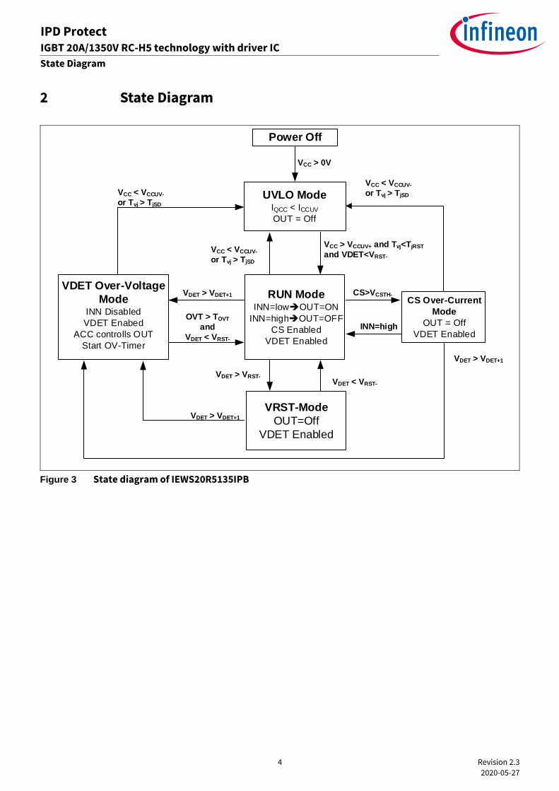
2 State Diagram
UVLO ModeIQCC < ICCUV
OUT = Off
VCC > VCCUV+ and Tvj<TjRST
and VDET<VRST-
Power Off
VDET Over-Voltage
ModeINN Disabled
VDET Enabed
ACC controlls OUT
Start OV-Timer
OVT > TOVT
and
VDET < VRST-
RUN ModeINN=lowOUT=ON
INN=highOUT=OFF
CS Enabled
VDET Enabled
CS>VCSTH-
VCC > 0V
CS Over-Current
Mode
OUT = Off
VDET EnabledINN=high
VCC < VCCUV-
or Tvj > TjSD
VCC < VCCUV-
or Tvj > TjSD
VCC < VCCUV-
or Tvj > TjSD
VDET > VDET+1
VDET > VDET+1
VRST-Mode
OUT=Off
VDET Enabled
VDET > VRST- VDET < VRST-
VDET > VDET+1
Figure 3 State diagram of IEWS20R5135IPB
5 Revision 2.3
2020-05-27
IPD Protect IGBT 20A/1350V RC-H5 technology with driver IC
Electrical Parameters Driver
3 Electrical Parameters Driver
3.1 Absolute Maximum Ratings
Absolute maximum ratings indicate sustained limits beyond which damage to the device may occur. All voltage parameters are absolute voltages referenced to COM, all currents are defined positive into any pin.
Table 1 Absolute Maximum Ratings
Parameter Symbol Min. Max. Unit Test Conditions
VDET pin voltage VDET
-0.3 VCLAMP 1
V
VCC pin voltage VCC
CS pin voltage CS
INN pin voltage INN -0.3 5 V
Junction temperature Tv j -40 150 °C
Storage temperature TS
ESD capability VESD 750 V Charged Devices Model (CDM) 2
ESD capability VESD 2.0 KV Human Body Model (HBM) 3
3.2 Recommended Operating Conditions
For proper operation the device should be used within the recommended conditions. (TA=25°C)
Table 2 Recommended Operating Conditions
Parameter Symbol Min. Max. Unit
VDET pin voltage VDET
-0.3 20 V VCC pin voltage VCC
CS pin voltage CS
INN pin voltage INN -0.3 5 V
Junction temperature Tv j -40 125 °C
1 This IC contains a 25V voltage clamp structure between the VCC and COM pins. Please note that this pin should not be driven by a DC,
low impedance power source greater than the VCLAMP specified in the Electrical Characteristics section. 2 According to the JESD22-C101 CDM standard 3 According to the JESD22-A114 Rev. F standard
6 Revision 2.3
2020-05-27
IPD Protect IGBT 20A/1350V RC-H5 technology with driver IC
Electrical Parameters Driver
3.3 Electrical Characteristics
VCC=15.0V, TA = 25 °C unless otherwise specified. All parameters are referenced to COM.
Table 3 VCC Characteristics
Parameter Symbol Min. Typ. Max. Unit Test Conditions
VCC rising UVLO threshold VCCUV+ 13.0 13.5 14.0 V
VCC falling UVLO threshold VCCUV- 12.0 12.5 13.0
VCC supply current during UVLO ICCUV --- 200 --- µA
VCC=VCCUV- -0.5V
VCC quiescent supply current IQCC --- 3000 ---
VCC internal Zener clamp voltage VCLAMP --- 25 --- V ICC=5mA
Table 4 CS Characteristics
Parameter Symbol Min. Typ. Max. Unit Test Conditions
Over-current threshold voltage VCSTH- -5% -0.2 +5% V
Over-current detection internal blank time tCSBLK 3.5 --- 4.5 µs
IPD Protect IGBT 20A/1350V RC-H5 technology with driver IC
Electrical Parameters Driver
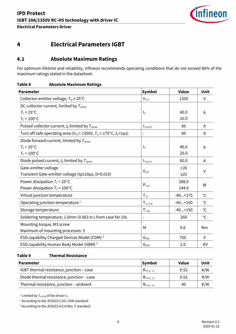
4 Electrical Parameters IGBT
4.1 Absolute Maximum Ratings
For optimum lifetime and reliability, Infineon recommends operating conditions that do not exceed 80% of the maximum ratings stated in the datasheet.
Table 8 Absolute Maximum Ratings
Parameter Symbol Value Unit
Collector-emitter voltage, Tvj ≥ 25°C V C E 1350 V
DC collector current, limited by Tvjmax
TC = 25C
TC = 100C
I C
40.0
20.0
A
Pulsed collector current, tp limited by Tvjmax I C p u l s 60 A
Turn off safe operating area (VCE 1350V, Tvj 175C, tp=1µs) - 60 A
Diode forward current, limited by Tvjmax
TC = 25C
TC = 100C
I F
40.0
20.0
A
Diode pulsed current, tp limited by Tvjmax I F p u l s 60.0 A
Gate-emitter voltage
Transient Gate-emitter voltage (tp≤10µs, D<0.010) V G E
20
±25 V
Power dissipation TC = 25C
Power dissipation TC = 100C P t o t
288.0
144.0 W
Virtual junction temperature T v j -40...+175 °C
Operating junction temperature 1 T v j , o p -40...+150 °C
Storage temperature T s t g -40...+150 °C
Soldering temperature, 1.6mm (0.063 in.) from case for 10s - 260 °C
Mounting torque, M3 screw
Maximum of mounting processes: 3 M 0.6 Nm
ESD capability Charged Devices Model (CDM) 2 VESD 750 V
ESD capability Human Body Model (HBM) 3 VESD 2.0 KV
Table 9 Thermal Resistance
Parameter Symbol Value Unit
IGBT thermal resistance, junction – case R t h ( j - c ) 0.52 K/W
Diode thermal resistance, junction – case R t h ( j - c ) 0.52 K/W
Thermal resistance, junction – ambient R t h ( j - a ) 40 K/W
1 Limited by Tvj,max of the driver IC. 2 According to the JESD22-C101 CDM standard 3 According to the JESD22-A114 Rev. F standard
9 Revision 2.2
2020-01-22
IPD Protect IGBT 20A/1350V RC-H5 technology with driver IC
Electrical Parameters Driver
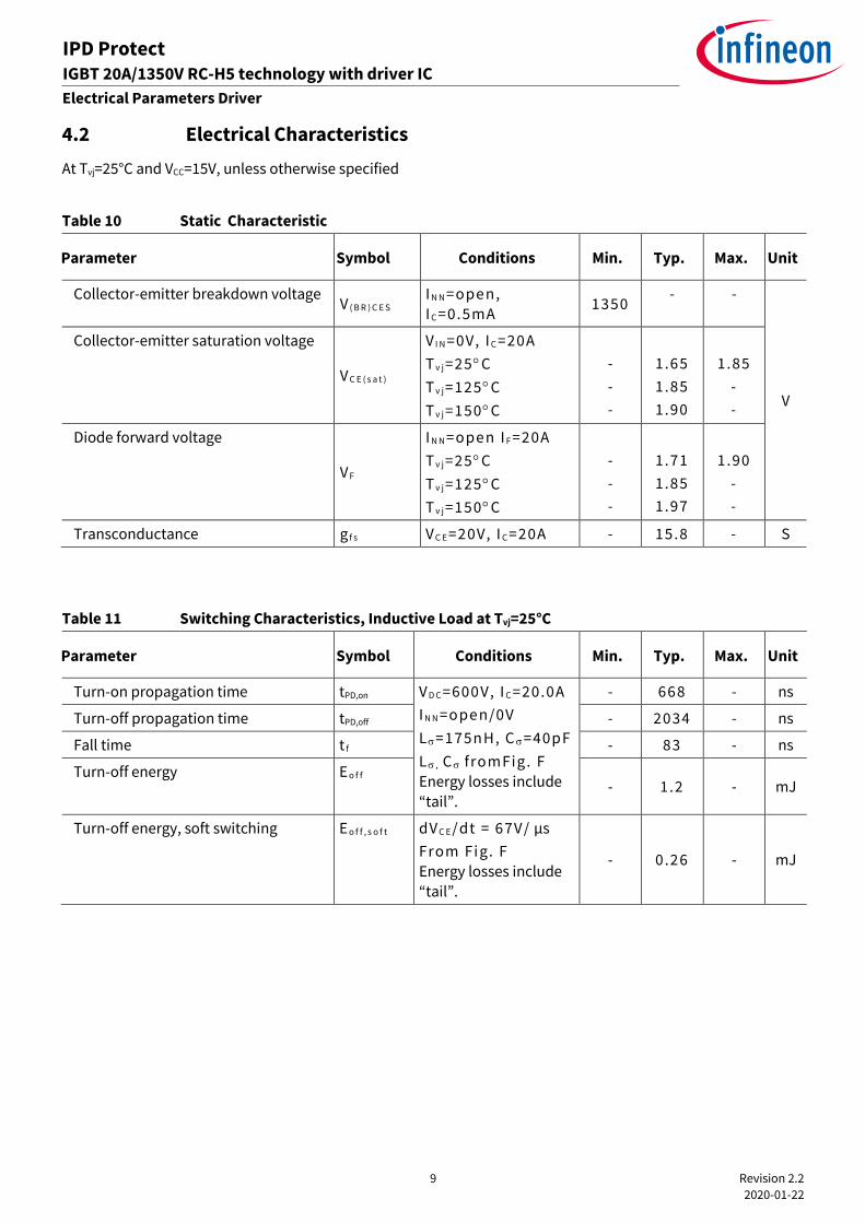
4.2 Electrical Characteristics
At Tvj=25°C and VCC=15V, unless otherwise specified
Table 10 Static Characteristic
Parameter Symbol Conditions Min. Typ. Max. Unit
Collector-emitter breakdown voltage V ( B R ) C E S
I N N =ope n, I C =0.5mA
1350 - -
V
Collector-emitter saturation voltage
V C E ( s a t )
V I N =0V, I C =20A
T v j =25C
T v j =125C
T v j =150C
-
-
-
1.65
1.85
1.90
1.85
-
-
Diode forward voltage
V F
I N N =ope n I F =20A
T v j =25C
T v j =125C
T v j =150C
-
-
-
1.71
1.85
1.97
1.90
-
-
Transconductance g f s V C E =20V, I C =20A - 15.8 - S
Table 11 Switching Characteristics, Inductive Load at Tvj=25°C
Parameter Symbol Conditions Min. Typ. Max. Unit
Turn-on propagation time tPD,on V D C =600V, I C =20.0A
I N N =ope n/0V
L=175nH, C=40pF
L , C fromFig. F Energy losses include
“tail”.
- 668 - ns
Turn-off propagation time tPD,off - 2034 - ns
Fall time t f - 83 - ns
Turn-off energy E o f f - 1.2 - mJ
Turn-off energy, soft switching E o f f , s o f t dV C E /dt = 67V/ µs
From Fi g. F Energy losses include
“tail”.
- 0.26 - mJ
10 Revision 2.2
2020-01-22
IPD Protect IGBT 20A/1350V RC-H5 technology with driver IC
Electrical Parameters Driver
Table 12 Switching Characteristics, Inductive Load at Tvj=150°C
Parameter Symbol Conditions Min. Typ. Max. Unit
Turn-on propagation time tPD,on V D C =600V, I C =20.0A
I N N =ope n/0V
L=175nH, C=40pF
L , C fromFig. F Energy losses include “tail”.
- 705 - ns
Turn-off propagation time tPD,off - 2257 - ns
Fall time t f - 231 - ns
Turn-off energy E o f f - 2.2 - mJ
Turn-off energy, soft switching E o f f , s o f t dV C E /dt = 67V/ µs
From Fi g. F
Energy losses include “tail”.
- 0.40 - mJ
11 Revision 2.2
2020-01-22
IPD Protect IGBT 20A/1350V RC-H5 technology with driver IC
Pin Configuration, Description and Functionality
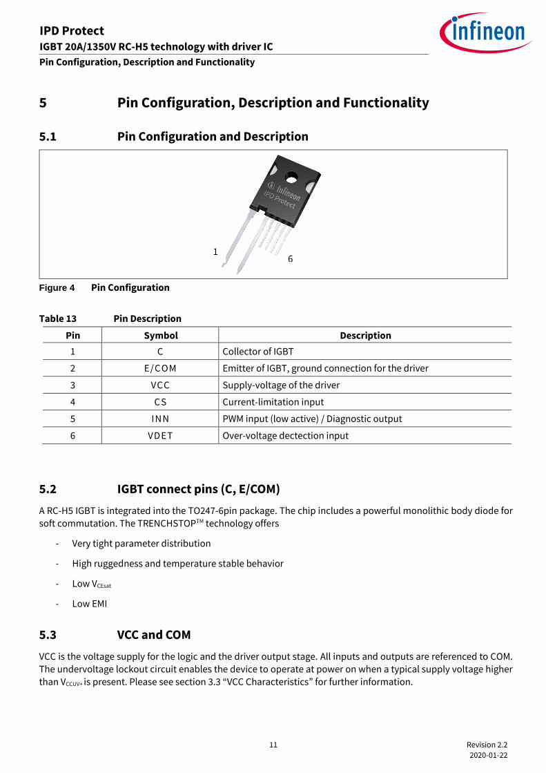
5 Pin Configuration, Description and Functionality
5.1 Pin Configuration and Description
Figure 4 Pin Configuration
Table 13 Pin Description
Pin Symbol Description
1 C Collector of IGBT
2 E/COM Emitter of IGBT, ground connection for the driver
3 VCC Supply-voltage of the driver
4 CS Current-limitation input
5 INN PWM input (low active) / Diagnostic output
6 VDET Over-voltage dectection input
5.2 IGBT connect pins (C, E/COM)
A RC-H5 IGBT is integrated into the TO247-6pin package. The chip includes a powerful monolithic body diode for soft commutation. The TRENCHSTOPTM technology offers
- Very tight parameter distribution
- High ruggedness and temperature stable behavior
- Low VCEsat
- Low EMI
5.3 VCC and COM
VCC is the voltage supply for the logic and the driver output stage. All inputs and outputs are referenced to COM. The undervoltage lockout circuit enables the device to operate at power on when a typical supply voltage higher than VCCUV+ is present. Please see section 3.3 “VCC Characteristics” for further information.
6 1
12 Revision 2.2
2020-01-22
IPD Protect IGBT 20A/1350V RC-H5 technology with driver IC
Pin Configuration, Description and Functionality
5.4 Current limitation input (CS)
The integrated cycle by cycle current limitation, given in the next figure, offers independent of the external control
and input-voltage level, a voltage limitation across the IGBT. The negative current sense threshold (VCSTH-) has the big advantage that the current sense resistor is not in the gate-drive loop. When the INN-input is switched to COM, the IGBT is turned on from the driver and the current-sense input gets enabled after a delay of tCSBLK, to avoid miss-
triggering during NZVS (Non Zero Voltage Switching) conditions. Once enabled, the voltage at the CS-pin gets monitored and when the current sense threshold is reached the IGBT turns off immediately, independent from
the signal at the INN-input. A resistor of 1kOhm should be placed in series to the CS input to limit currents through the internal ESD-diodes due to transients.
VCE
time
VCSTH-
OnTime
Off Time
time
VRCS
time
INN
OCP Event OCP Event
Figure 5 Cycle by cycle current limitation
5.5 PWM input / Diagnostic output (INN)
The INN pin is a multifunctional pin. It acts as an input to control the ON-time of the IGBT and during the OFF-time, the diagnostic block controls the pull-up voltage level according to the status (see Table 14 & Figure 8).
To control the turn-on of the IGBT an open drain output should be connected to the INN pin. The Schmitt trigger
input is such to guarantee compatibility down to 3.3V controller. The input Schmitt trigger and noise filter provide beneficial noise rejection to short input pulses according to Figure 6 and Figure 10.
13 Revision 2.2
2020-01-22
IPD Protect IGBT 20A/1350V RC-H5 technology with driver IC
Pin Configuration, Description and Functionality
VCC
Input Noise Filter
Diagnostic with
Pullup ControlINN
VIL, VIH
Microcontroller
ON-Time Control
A/D Converter
or Comparator
PWM
IEWS20R5135IPB
Figure 6 INN internal structure
Table 14 INN Diagnostic Pullup-Levels
Status Pull-up Level (INN)
UVLO <0,5V
No Fault 2,10V – 2,90V
OT-Warning 4V – 5V
OV-Detection <0,5V
OT-Warning +
OV-Detection
<0,5V
(OV dominates)
OT-Shut-Down <0,5V
5.6 Over-voltage detection input (VDET)
The integrated active clamp control level can be programmed on the VDET input with the resistor devider
R1, R2 (Figure 7). After fixing R1, R2 can be calculated with the following equation:
𝑅2 = 𝑅1
𝑉𝑐𝑙𝑎𝑚𝑝1
𝑉𝐷𝐸𝑇+1− 1
VClamp = programmed clamping level
VDET+1 = internal VDET+1 threshold
When the voltage at VDET goes above the internal threshold of VDET1+ , the Active Clamp Control (ACC) takes over and turns on the IGBT in order to regulate the voltage at VDET to VDET+1 and therefore the collector voltage to the
programmed level VClamp1. After the time Tclamp1 the internal clamping level is increased by 11%. The ACC stay’s active until the voltage at VDET drops below VDET1+ within Tclamp1 or below VDET2+ after Tclamp1. A third internal threshold at VDET (VRST-) takes care, that the IGBT is not turned on at a too high voltage level.
Therefore the driver stay’s disabled until the VDET voltage drops below VRST-. The restart level (VRST-) can be calculated with following equation:
𝑉𝑅𝑆𝑇 = 𝑉𝑐𝑙𝑎𝑚𝑝1 ∗𝑉𝑅𝑆𝑇−
𝑉𝐷𝐸𝑇+1
In normal operation the VRST- threshold is also active and blocks the turn-on of the IGBT until the VDET voltage falls below VRST-, but the INN is not switched to GND compared to the OV-detection mode (Table 15). If the INN is
switched to GND from the control system when the VCE>VRST- the complete cycle is skipped (see Figure 9).
14 Revision 2.2
2020-01-22
IPD Protect IGBT 20A/1350V RC-H5 technology with driver IC
Pin Configuration, Description and Functionality
For short clamp situations, which can occur for example when the vessel is removed from the cooking surface, an
over-voltage timer (OVT) is triggered in parallel. The OVT disables the driver for the over-voltage blank time so that the connected microcontroller has time to recognize and to react on the situation.
IEWS20R5135IPB
VCC
VDETVDET+, VRST-
Active Clamp Control
Over-Voltage Timer
C
E/COM
R1
R2
Figure 7 Active Clamp Control setting
VCE
time
VDET+1
OUT
time
On-Time Off-Time
Over-Voltage Mode
Restart from the microNormal Operation
VRST-
Over-Voltage Detection
time
INN
Normal Mode
2.5V
4.5V
No Fault or Warning
OV-Detection
OT-Warning
No Fault or Warning
Driver release IN with OT-Warning (3V)
MCU recognize and restarts with SS
Active ClampControl
time
OVT
tOVT
tclamp1
VDET+2
Figure 8 Active Clamp Control timing & Diagnostic
15 Revision 2.2
2020-01-22
IPD Protect IGBT 20A/1350V RC-H5 technology with driver IC
Pin Configuration, Description and Functionality
VCE
VDET+1
OUT
On-Time Off-Time
VRST-
INN
2.5V
Complete cycle is skipped
Turn-onVCE>VRST-
Figure 9 Function turn-on, if VCE>VRST-
16 Revision 2.2
2020-01-22
IPD Protect IGBT 20A/1350V RC-H5 technology with driver IC
Timing Diagrams
6 Timing Diagrams
INN
OUT
tONfilter tONfilter
a) b)
tOFFfilter
CS
-0.2V
c)tONfilter tOFFfilter
-0.2V
INN
OUT
CS
tONfilter tOFFfilter
d)
1
1
1 Short pulses below the filter-time are suppressed
Figure 10 Input Noise Filter
INN
tONfilter tOFFfilter
OUTShort-CircuitDrive-Current
tO1+
IO1+
IO2+
0A
IO-
Figure 11 OUT Short-Circuit Drive-Current
17 Revision 2.2
2020-01-22
IPD Protect IGBT 20A/1350V RC-H5 technology with driver IC
Electrical Characteristics Diagrams
7 Electrical Characteristics Diagrams
UVLO ON/OFF
vs
TEMPERATURE
UVLO HYSTERESIS
vs
TEMPERATURE
11.6
12.0
12.4
12.8
13.2
13.6
14.0
14.4
-50 -25 0 25 50 75 100 125 150
VCCU
V[V
]
Tvj, JUNCTION TEMPERATURE [°C]
0.0
1.0
2.0
3.0
-50 -25 0 25 50 75 100 125 150
VCCU
V_
HYST
[V]
Tvj, JUNCTION TEMPERATURE [°C]
VCCUV +
VCCUV -
V INL / V INH
vs
TE MP E R ATUR E
0.4
0.8
1.2
1.6
2.0
2.4
2.8
-50 -25 0 25 50 75 100 125 150
VIL
/ V
IH[V
]
Tvj, JUNCTION TEMPERATURE [°C]
VIL
VIH
Figure 12. Undervoltage Lockout
Figure 13. Input Voltage Characteristic
18 Revision 2.2
2020-01-22
IPD Protect IGBT 20A/1350V RC-H5 technology with driver IC
Electrical Characteristics Diagrams
CURRENT CONSUMPTION vs
TEMPERATURE CURRENT CONSUMPTION vs
OPERATING SUPPLY VCC
CURRENT CONSUMPTION
vs
FREQUENCY
0.0
2.0
4.0
6.0
8.0
-50 -25 0 25 50 75 100 125 150
Cu
rre
nt
[m
A]
Tvj, JUNCTION TEMPERATURE [°C]
Series1
Series2
0.0
1.0
2.0
3.0
4.0
5.0
0 5 10 15 20 25
Cu
rre
nt
[mA
]
VCC [V]
0
4
8
12
16
0 25 50 75 100
Cu
rre
nt
[m
A]
Frequency [kHz]
VCC = 15V
IQCC(VCC=15V) IQCCUV(VCC=15V
(INN floating) (Tvj = 25°C, INN floating)
UVLO region
19 Revision 2.2
2020-01-22
IPD Protect IGBT 20A/1350V RC-H5 technology with driver IC
Electrical Characteristics Diagrams
INN
vs
TE MPE R ATUR E
V IP Uov
vs
TE MPE R ATUR E
V DE T + 1, V DE T + 2, V R S T -
vs
TE MPE R ATUR E
V C S T H -
vs
TE MPE R ATUR E
tC S B L K
vs
TE MPE R ATUR E
0
2
4
6
8
10
-50 -25 0 25 50 75 100 125 150
VIN
N[V
]
Tvj, JUNCTION TEMPERATURE [°C]
0.0
3.0
6.0
9.0
-50 -25 0 25 50 75 100 125 150
VD
ET+
1,
VD
ET+
2,
VR
ST-[V
]
Tvj, JUNCTION TEMPERATURE [°C]
-225
-218
-211
-204
-197
-190
-183
-50 -25 0 25 50 75 100 125 150
VCSTH
-[V
]
Tvj, JUNCTION TEMPERATURE [°C]
0.000
0.002
0.004
0.006
0.008
0.010
-50 -25 0 25 50 75 100 125 150
VIP
Uov
[V]
Tvj, JUNCTION TEMPERATURE [°C]
VIPUov
0.0
3.0
6.0
9.0
-50 -25 0 25 50 75 100 125 150
t CSB
LK
[
S]
Tvj, JUNCTION TEMPERATURE [°C]
Figure 15. INN vs Tvj Figure 16. VIPUov vs Tvj
Figure 17. VDET+1, VDET+2, VRST- vs Tvj
Figure 18. VCSTH- vs Tvj
Figure 19. tCSBLK vs Tvj
VDET+1
VDET+2
VRST-
VINN VIPUov
VCSTH-
tCSBLK
OTW
region
20 Revision 2.2
2020-01-22
IPD Protect IGBT 20A/1350V RC-H5 technology with driver IC
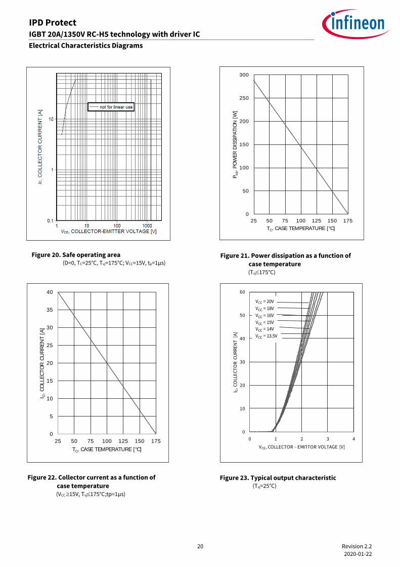
Electrical Characteristics Diagrams
Figure 20. Safe operating area (D=0, TC=25°C, Tvj=175°C; VCC=15V, tp=1μs)