Iris: A Hybrid Nanophotonic Network Design for High-Performanceand Low-Power on-Chip Communication
ZHENG LI, MOUSTAFA MOHAMED, XI CHEN, HONGYU ZHOU, ALAN MICKELSON,LI SHANG, and MANISH VACHHARAJANI, University of Colorado at Boulder
On-chip communication, including short, often-multicast, latency-critical coherence and synchronizationmessages, and long, unicast, throughput-sensitive data transfers, limits the power efficiency and perfor-mance scalability of many-core chip-multiprocessor systems. This article analyzes on-chip communicationchallenges and studies the characteristics of existing electrical and emerging nanophotonic interconnect.Iris, a CMOS-compatible high-performance low-power nanophotonic on-chip network, is thus introduced.Iris’s circuit-switched subnetwork supports throughput-sensitive data transfer. Iris’s optical-antenna-array-based broadcast–multicast subnetwork optimizes latency-critical traffic and supports the path setup ofcircuit-switched communication. Overall, the proposed nanophotonic network design offers an on-chip com-munication backplane that is power efficient while demonstrating low latency and high throughput.
Categories and Subject Descriptors: C.1.2 [Processor Architectures]: Multiple Data Stream Architectures(Microprocessors)—Interconnection Architectures
General Terms: Design, Performance
Additional Key Words and Phrases: Nanophotonics, Networks-on-chip, Optical interconnects, Interconnec-tion networks
ACM Reference Format:Li, Z., Mohamed, M., Chen, X., Zhou, H., Mickelson, A., Shang, L., and Vachharajani, M. 2011. Iris: A hybridnanophotonic network design for high-performance and low-power on-chip communication. ACM J. Emerg.Technol. Comput. Syst. 7, 2, Article 8 (June 2011), 22 pages.DOI = 10.1145/1970406.1970410 http://doi.acm.org/10.1145/1970406.1970410
1. INTRODUCTION
Fabrication technology scaling has steadily improved the performance and power effi-ciency of transistors. The performance and power dissipation of global metal wires havenot scaled correspondingly. They are consuming an increasing portion of the overallsystem power budget. As a result, core-to-core communication is perceived as the majorobstacle in scaling parallel program performance of many-core chip multiprocessors.
To address this challenge, attention is focused on new electrical and photonicon-chip communication solutions. Packet-switched electrical interconnect fabrics,widely used in chip-to-chip multiprocessor computer systems, have been graduallyadopted in application-specific multiprocessor system-on-chips and general-purposechip-multiprocessors. As demonstrated by recent academic and industrial chip de-signs, for instance, TRIPS [Gratz et al. 2007] and Intel’s 48-core Single-Chip Cloud
ACM Journal on Emerging Technologies in Computing Systems, Vol. 7, No. 2, Article 8, Pub. date: June 2011.
8:2 Z. Li et al.
Broadcast network
Channel waveguides
Antenna array
Si
Si
SiO2
Si
Micro-ring resonators
Silicon-siliconinterconnect
Metal wires
CMOS devicesThrough Silicon via
Package
Electricalpower pad
Laser power
Circuit-switched network
Fig. 1. Schematic of Iris.
Computer [Howard et al. 2010], packet-switched electrical interconnect provideshighly-scalable throughput at large processor counts.
Electrical interconnect fabric is far from ideal in terms of power efficiency and perfor-mance scalability. Packet-switched electrical networks introduce excess and variablelatency because of runtime multihop data buffering, resource arbitration, and link con-tention. In addition, they consume a large portion of the total chip power (e.g., 28% in a80-node mesh network [Hoskote et al. 2007]). As the number of on-chip processor coresincreases, worst-case latency and power consumption suffer as the average number ofhops per packet increases.
Photonics promises far better performance and power efficiency than electricalcounterparts [Beausoleil et al. 2008; Krishnamoorthy et al. 2010]. Recently proposednanophotonic on-chip interconnects have demonstrated exceptional throughput withlow power dissipation [Kirman et al. 2006; Shacham et al. 2008; Vantrease et al. 2008;Batten et al. 2008; Joshi et al. 2009; Cianchetti et al. 2009; Miller et al. 2009; Pan et al.2009; Xue et al. 2010; Koka et al. 2010] (See Section 7 for details).
However, there are still challenges that existing optical interconnects do not ad-dress, both in terms of architecture and fabrication. In many-core systems, on-chiptraffic can be classified into two categories (see Section 2.1). The first are short, often-multicast, and latency-critical coherence and synchronization messages. The secondare throughput-bound, often-unicast data transfers, such as cache line flushes. Eventhough latency-critical traffic is only a small portion of total bits transferred on thenetwork, if not properly handled, system performance can degrade significantly [Jergeret al. 2008]. Unfortunately, design decisions centered around fabrication limitations ofoptical components mean that these messages are not handled well. In particular, itis difficult to fabricate optical buffers in a CMOS compatible manner [Beausoleil et al.2008], which means that the more scalable optical approaches are circuit-switched.In existing solutions, the circuit-switched path setup significantly increases the la-tency of short synchronization messages. Worse, these messages are often broadcastor multicast and thus incurring the cost of setting up multiple circuits and retrans-mitting messages over these multiple circuits, further driving up latency and powerconsumption.
In order to build a low power nanophotonic on-chip network to suit the abovediscussed requirements, we investigate the characteristics of on-chip electrical andnanophotonic interconnects in detail. Based on this study, we propose Iris, a CMOS-compatible, low-latency, high-throughput, and low-power nanophotonic on-chip net-work. As shown in Figure 1, Iris is a multilayer design, consisting of a low-latencybroadcast/multicast nanophotonic subnetwork and a throughput-optimized circuit-switched subnetwork that employs photonic channel waveguides. This dual networkdesign delivers exceptionally low latency and high throughput with minimal powerdissipation by:
ACM Journal on Emerging Technologies in Computing Systems, Vol. 7, No. 2, Article 8, Pub. date: June 2011.
Iris: A Hybrid Nanophotonic Network Design on-Chip Communication 8:3
(1) optimizing the delivery of short latency-bound broadcast messages on the low-latency broadcast subnetwork and long throughput-hungry unicast messages onthe throughput-optimized subnetwork;
(2) minimizing path setup time for the circuit-switched throughput-optimized networkby using broadcast messages sent over the low-latency broadcast subnetwork;
(3) minimizing power dissipation by using efficient optical communication for multi-cast, path setup, and high-throughput data-transfer.
The net result is an interconnect fabric with high throughput, low latency, andlow power dissipation. Simulation results show that, compared with other recentlyproposed electrical and nanophotonic networks, Iris improves performance by a rangeof 7.2% to 49.9%. and power efficiency by a range of 1.8% to 92.7%.
The rest of this article is organized as follows. Section 2 analyzes the workloadcharacteristics of emerging many-core on-chip systems, and investigates in detail theperformance and power characteristics of on-chip photonic and electrical communica-tion technologies. Section 3 presents an overview for Iris, the proposed nanophotonicon-chip network design. Section 4 and Section 5 describe the architecture-level andphysical-level designs, respectively. Section 6 evaluates Iris, and Section 7 presentsrelated works.
2. MOTIVATIONS AND MODELS
This section analyzes the on-chip communication traffic workload (Section 2.1), andinvestigates the performance and power characteristics of on-chip electric (Section 2.2)and photonic interconnect (Section 2.3). This study motivates the proposed design(Section 3).
2.1. Characterizing On-Chip Traffic
In many-core systems, on-chip traffic is heterogeneous. Part of the traffic is intendedto synchronize thread execution, coordinate distributed data placement, and allocateglobal resources. It consists of short, latency-critical, and often-multicast protocol mes-sages. The other part of the traffic transfers data between cores and usually consistsof long, throughput-hungry and often-unicast data packets.
Consider a cache-coherent shared-memory many-core system. To complete one datatransaction, triggered by a read or write cache miss, a request protocol message is firstsent out to locate valid cache line copies. This message, containing only the memoryaddress and the processor ID, is usually short. Once data is located, cache lines con-taining large data packets are transferred back to the requester. To locate cache copiesquickly, broadcasting the request protocol message is preferred, as is found in variousprotocols, for instance, Snoopy, Token Coherence, etc. Otherwise, directory indirectionis incurred which slows the whole transaction.
The two classes of traffic have different characteristics. Sending short protocolmessages to multiple destinations in a unicast network worsens the overall proto-col message deliver latency, which is determined by the slowest path. A recent studyshows that even if multicast messages represent only a small portion of on-chip traf-fic, the overall network latency and throughput can degrade substantially, negatingthe point-to-point efficiency and performance advantages [Jerger et al. 2008]. It iscrucial to provide a broadcast/multicast interconnect fabric to minimize, or share,multiple path setup latencies and reduce the broadcast-induced bursty contention.On the other hand, for transferring throughput-hungry data messages, which aretypically hundreds of bytes long, serialization and contention dominate the overalllatency. To minimize their latencies, communication links need to be shared effectivelyso as to sustain a scalable high throughput.
ACM Journal on Emerging Technologies in Computing Systems, Vol. 7, No. 2, Article 8, Pub. date: June 2011.
8:4 Z. Li et al.
2.2. Characterizing Electrical Interconnect
The lack of power and latency scalability limits electrical interconnect’s potential tosatisfy global on-chip communication requirements, especially for those often-multicastlatency-critical protocol messages.
Fundamentally, neither propagation delay nor power consumption of global electri-cal wires scales with technology advances. The propagation delay of metal wires isquadratic in the propagation distance L and is proportional to the electrical RC timeconstant. The energy required to send information over wire is determined by the wirecapacitance and swing voltage as CV 2
DD L. Numerically, ITRS [2008] shows that, from65nm to 32nm technology, the signal propagation delay in a 1mm minimal-pitch globalcopper wire increases from 227ps to 1129ps, and the power index range (dynamicpower per unit frequency per unit area of one metal layer) for global wires increasesfrom 1.4–1.6 to 1.7–2.0W/GHz-cm2.
Routers or switches, which are used to share the segmented wiring resources, intro-duce excessive and nondeterministic latency for arbitration, switching, and contention.These operations require significant power overhead. Consider the recently developed45 nm Intel Single-Chip Cloud Computer [Howard et al. 2010]. The router in this 4-by-6 mesh network includes four pipeline stages. To traverse the network withoutcontention, a packet would take at most 10 hops, where each hop is 5 clock cycles.Besides, each router consumes 500mW power, contributing to 10% of the tile powerconsumption. Multicast protocol traffic can further exacerbate this situation. As thenumber of on-chip processor cores increases, worst-case latency and power consumptionsuffer as the average number of hops per packet will increase. As the technology scales,the increasing leakage power, especially in router buffers, will worsen this situation.
2.3. Characterizing Photonic Interconnect
In principle, nanophotonics can offer orders-of-magnitude performance and power im-provement over the electrical counterparts [Beausoleil et al. 2008]. However, on-chipnanophotonic interconnect exhibits unique characteristics. Electrical network designswith photonic wires cannot unleash the potential of photonic interconnect. In thissection, models of the nanophotonic interconnect demonstrate a unique method forhandling heterogeneous traffic. As part of our efforts in characterizing and modelingnanophotonic devices, we have fabricated three batches of devices in ePIXfab [2008]and measured them in our labs. Specifically, we have fabricated devices using 193nmdeep UV lithography on 200mm silicon-on-insulator (SOI) wafers with 220nm top Sifilm and 2000nm buried oxide. Where noted, we also use recently published results ofother groups that have employed similar SOI process technology. The analysis belowis guided by our results from the physical study of these devices.
2.3.1. Overview. The components in an on-chip nanophotonic interconnect mimic thosefound in optical telecommunication systems. The link consists of a light source, trans-mitters, waveguides, and receivers. Except for the light source, other components havebeen successfully integrated on-chip over the years [Beausoleil et al. 2008]. The on-chipwaveguide delivers optical power from an off-chip light source. Transmitters [Chenet al. 2009; Zheng et al. 2010a], comprised of modulators and filters, modulate thedigital data stream generated by processing/storage components to the selected lightwavelengths. Photonic signals are carried and routed to various on-chip destinationsvia on-chip waveguides and broadband routing switches, which have recently been con-structed of racetrack resonators [Chen et al. 2010]. Once the optical signals arrive attheir destination, the receiver demultiplexes each wavelength via ring resonator basedfilters [Little et al. 1998]. Photonic signals are then converted into electrical current
ACM Journal on Emerging Technologies in Computing Systems, Vol. 7, No. 2, Article 8, Pub. date: June 2011.
Iris: A Hybrid Nanophotonic Network Design on-Chip Communication 8:5
via epitaxially grown Ge detectors and are amplified by CMOS circuitry [Koester et al.2007; Chen et al. 2009; Zheng et al. 2010b].
2.3.2. Performance. Nanophotonic interconnect offers low-latency data propagationand ultra-wide bandwidth by leveraging wavelength-division multiplexing (WDM) andtime-division multiplexing (TDM). Therefore, the latency of a packet is significantly re-duced compared to the electrical solution. The main overhead is due to the serializationlatency to transfer large packets in multiple clock cycles, the circuit path setup latency,and the electrical to and from optical conversion latency at the transceiver ends. Thesethree sources of overhead may be reduced by innovation in network design.
2.3.3. Power. The power consumption of a nanophotonic on-chip network consists ofboth the optical power lost in propagation and electrical power consumed in the elec-trical control circuitry.
Off-chip light sources cannot presently be controlled dynamically by on-chip traf-fic. Optical power then is usually statically allocated by a worst-case aggregated lossbudget. Total optical power is given by:
Pstatic = Poptical = Pdetect
/ ∏i
(1 − ηi
loss
), (1)
where ηiloss is the proportional power loss at the ith component along the signal prop-
agation path, and Pdetect is the required optical power for arrival at the photodetector,that is, the sensitivity of photodetector. If the optical power needs to be delivered tomultiple locations sequentially, the increasing number of ηi
loss would inevitably lead tosignificant growth of Poptical .
Numerically, the worst case optical loss budget analysis has to account for variouscomponents, including: the grating coupler loss which may reach 1.6dB [Vermeulenet al. 2009], straight waveguide loss which is 1.34dB/cm [Selvaraja et al. 2009], waveg-uide bend loss which is approximately 0.086dB for a bending radius of 1μm [Vlasovand McNab 2004], waveguide crossing loss which may reach 0.045dB/crossing [Popovicet al. 2007], micro-ring based filters which have a loss of 1–2dB depending on thedimension [Xiao et al. 2007], and micro-ring based modulators which have a loss of2dB and an extinction ratio of 9dB [Chen et al. 2009]. Finally, sensitivity of currentphotodetectors, Pdetect , is less than 1μW based on the design demonstrated by Sahniet al. [2008] and analysis of Beausoleil et al. [2008] (where sensitivity is defined bythe electrical signal to noise ratio required in order to achieve a bit error rate (BER) of10−12 in a typical threshold detection digital repeater).
Other important components of the nanophotonic power are the electrical power atthe transceivers to convert from optical to electrical domains and back and the electricalpower necessary to drive photonic switches. This power is given by:
where Ptransmitter is the power to modulate the electrical signal onto the light carrierat the transmitter, Preceiver is the power to convert the optical signal back into an elec-trical signal at the receiver, and Pswitch is the power necessary to route the photonicsignal to its destination. The power for each component includes the electrical circuitrydissipation and the expended power tuning devices to the proper passband. Transmit-ters and switches are usually designed with ring resonators whose operating energyhas been demonstrated to be 2pJ/bit [Lee et al. 2010], while receivers’ per bit energyconsumption is in the order of 690fJ/bit [Zheng et al. 2010b].
2.3.4. Functionality. Photonic on-chip interconnect is bufferless in the foreseeable fu-ture. The circuit-switched nature of nanophotonic interconnect directly affects the
ACM Journal on Emerging Technologies in Computing Systems, Vol. 7, No. 2, Article 8, Pub. date: June 2011.
8:6 Z. Li et al.
Transmitter
Receiver
Switch
Antenna feed
(a) Top down conceptual diagram of messagetransmissions in Iris
Transmitter
Receiver
Waveguide
Antenna
(b) Layout of the broadcast network
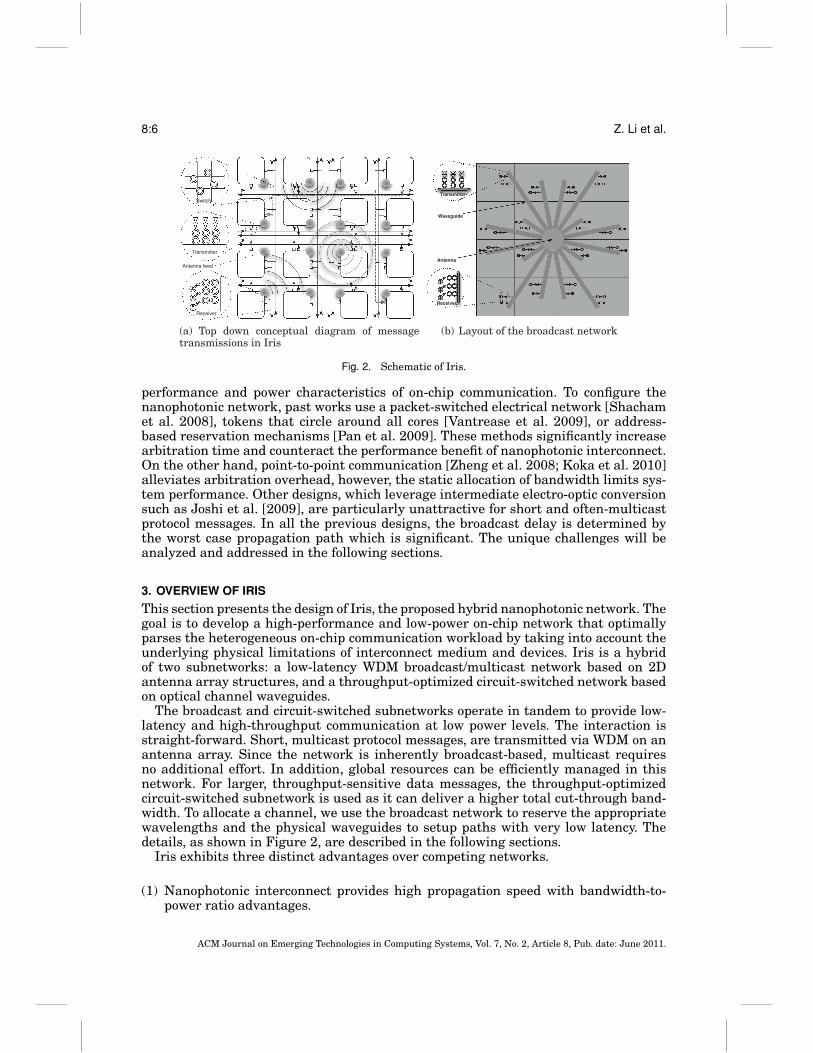
Fig. 2. Schematic of Iris.
performance and power characteristics of on-chip communication. To configure thenanophotonic network, past works use a packet-switched electrical network [Shachamet al. 2008], tokens that circle around all cores [Vantrease et al. 2009], or address-based reservation mechanisms [Pan et al. 2009]. These methods significantly increasearbitration time and counteract the performance benefit of nanophotonic interconnect.On the other hand, point-to-point communication [Zheng et al. 2008; Koka et al. 2010]alleviates arbitration overhead, however, the static allocation of bandwidth limits sys-tem performance. Other designs, which leverage intermediate electro-optic conversionsuch as Joshi et al. [2009], are particularly unattractive for short and often-multicastprotocol messages. In all the previous designs, the broadcast delay is determined bythe worst case propagation path which is significant. The unique challenges will beanalyzed and addressed in the following sections.
3. OVERVIEW OF IRIS
This section presents the design of Iris, the proposed hybrid nanophotonic network. Thegoal is to develop a high-performance and low-power on-chip network that optimallyparses the heterogeneous on-chip communication workload by taking into account theunderlying physical limitations of interconnect medium and devices. Iris is a hybridof two subnetworks: a low-latency WDM broadcast/multicast network based on 2Dantenna array structures, and a throughput-optimized circuit-switched network basedon optical channel waveguides.
The broadcast and circuit-switched subnetworks operate in tandem to provide low-latency and high-throughput communication at low power levels. The interaction isstraight-forward. Short, multicast protocol messages, are transmitted via WDM on anantenna array. Since the network is inherently broadcast-based, multicast requiresno additional effort. In addition, global resources can be efficiently managed in thisnetwork. For larger, throughput-sensitive data messages, the throughput-optimizedcircuit-switched subnetwork is used as it can deliver a higher total cut-through band-width. To allocate a channel, we use the broadcast network to reserve the appropriatewavelengths and the physical waveguides to setup paths with very low latency. Thedetails, as shown in Figure 2, are described in the following sections.
Iris exhibits three distinct advantages over competing networks.
(1) Nanophotonic interconnect provides high propagation speed with bandwidth-to-power ratio advantages.
ACM Journal on Emerging Technologies in Computing Systems, Vol. 7, No. 2, Article 8, Pub. date: June 2011.
Iris: A Hybrid Nanophotonic Network Design on-Chip Communication 8:7
(2) Hybrid interconnect design matches the heterogeneous requirements of on-chipcommunication.
(3) The novel broadcast network liberates the on-chip network from delivering multi-cast short messages which require expensive hop-by-hop arbitration for multiplecommunication resources.
4. IRIS: NETWORK ARCHITECTURE DESIGN
This section describes the architecture-level designs of Iris’s hybrid broadcast/circuit-switched network. In Iris, broadcast subnetwork handles short, multicast-like coher-ence protocol messages and coordinates the global interconnect resources, while thecircuit-switched subnetwork transfers large throughput-hungry data packets.
4.1. Low-Latency Broadcast Subnetwork
The broadcast subnetwork collects signals from all on-chip cores into a central smallantenna array, where signals are broadcast and distributed to all cores as shown inFigure 2(b). The WDM channels in this subnetwork are divided into several channelgroups. Each channel group is able to deliver all bits in one short protocol messagesimultaneously.
The broadcast subnetwork provides full-connectivity and serves two kinds of traffic.
(1) Short, latency-critical, often-multicast messages, which are used by coherence pro-tocols and synchronization mechanisms, and are on the critical path of systemperformance. The broadcast nature of the subnetwork provides a global order forevents and thus simplifies the system level coherence and synchronization.
(2) Global resource arbitration messages for both broadcast and circuit-switched net-work path setup. As the broadcast network has global reach with low latency, itenables an efficient resource allocation mechanism.
The key logical design consideration for the broadcast network is how to performarbitration, that is, determining the sequence of concurrent protocol message requests.To do this, we leverage the broadcast nature of the subnetwork and WDM. The netresult is a distributed global arbitration scheme that provides high broadcast through-put as well as low arbitration latency. Figure 3(a) illustrates the arbitration process.W nodes can leverage W wavelengths in the broadcast subnetwork to arbitrate for oneshared resource. One broadcast arbitration operation is followed by multiple broad-cast protocol messages. The arbitration scheme starts with each node being assigneda unique dynamic priority. Each node broadcasts a signal “1” on the wavelength corre-sponding to its dynamic priority. For example, as shown in Figure 3(a), in an eight-nodenetwork, three nodes, A, C and D, want to access a shared communication resource.Node A can broadcast on W1 (denoted [− − − − − − 1−]), Node C can broadcast on W6([−1 − − − − − −]), and Node D can broadcast on W2 ([− − − − −1 − −]). As the nodesends the one-bit message, it also listens for the combined messages broadcast acrossall wavelengths. If multiple nodes try to access the same resource, they will see thesame bit vector, reflecting the dynamic priorities of all the requesting nodes. For exam-ple, if Node A, C, and D arbitrate for the same set of wavelengths (i.e., the same channelgroup), they will all see a combined priority vector of [−1−−−11−], the bit-wise OR ofNode A, C, and D’s dynamic priorities. Then, each participating node in arbitration willgain accesses to the broadcast network in a sequence corresponding to the requesters’dynamic priorities. The number of protocol messages equals the number of requestersin the arbitration. The node with highest priority will be able to broadcast the mul-tidestinationed protocol messages in the next broadcast time slot after a quick checkwith OR gates. Other nodes will have to keep checking until their turn arrives. Aftereach arbitration, each node changes its dynamic priority using a deterministic random
ACM Journal on Emerging Technologies in Computing Systems, Vol. 7, No. 2, Article 8, Pub. date: June 2011.
8:8 Z. Li et al.
A
C
D
broadcast
receive
broadcast
receive
broadcast
receive
W7 W0
Time slots0 1 2 3 4 5 6 7
Wa
ve
len
gth
slo
ts
8 9 10 11
Un
ica
st a
rbitra
tion
Pro
toco
l me
ssa
ge
Pro
toco
l me
ssa
ge
Pro
toco
l me
ssa
ge
Bro
ad
ca
st a
rbitra
tion
Bro
ad
ca
st a
rbitra
tion
Pro
toco
l me
ssa
ge
Bro
ad
ca
st a
rbitra
tion
Un
ica
st a
rbitra
tion
Un
ica
st a
rbitra
tion
Un
ica
st a
rbitra
tion
Un
ica
st a
rbitra
tion
Un
ica
st a
rbitra
tion
Un
ica
st a
rbitra
tion
Sta
tus
up
da
te
Sta
tus
up
da
te
Sta
tus
up
da
te
Sta
tus
up
da
te
(a) Single-cycle arbitration and arbitration protocol in broadcast network
IdleNeed to send a new protocol
message?
Request1. Wait till a broadcast arbitration time slot
2. Broadcast "1" on the wavelength slot
corresponds to dynamic priority
AcknowledgementUse OR gate to check IDs of
other requesting nodes.
Am I the highest priority?
BroadcastSend the protocol message
over the broadcast
subnetwork
No
Yes
Receive
Yes
Complete
No WaitWait one cycle and remove
the current highest priority
node
Check
(b) FSM in broadcast network
IdleIs there a new unicast data
message?
Request 1. Wait till a unicast arbitration slot
2. Broadcast "1" on the wavelength
corresponding to dynamic priority
AcknowledgementUse OR gate to check IDs of other requesting nodes.
Am I the highest priority?
If status update info is also received, is it conflict free?
BroadcastSend the status update
information over the
broadcast network
No
Yes
Receive
Yes
Complete
Both
Yes
CheckUpdate and read the
occupation table.
Is all the path segments to the
destination free?
UnicastSend the data message
over the circuit switch
unicast network
Either is No
Yes
No
(c) FSM in unicast network
Fig. 3. Arbitration and arbiter’s finite state machine (FSM).
number generator. Since all nodes share the same random seed, they always agree onthe same global priority. Figure 3(b) illustrates the state transition in broadcastingprotocol messages.
To arbitrate for the same K resources, that is, multiple broadcast channel groups, Wnodes can still leverage W wavelengths in the broadcast network. The only differenceis that each node will be pre-assigned a channel group ID for arbitration. The arbitra-tion scheme turns to K (W/K) : 1 arbitration in parallel. This design sacrifices somearbitration efficiency for reduced arbitration latency and simplified arbitration logic.
From an architecture point of view, the throughput-optimized subnetwork is a circuit-switched mesh network using photonic channel waveguides. There are horizontal andvertical waveguides between each row and each column of processors in a many-coresystem, as is depicted in Figure 2(a). Dimension order routing is used for its minimaldistance and for simplicity of path setup. The broadcast subnetwork provides a low-latency means of allocating routing paths for long data messages.
The preceding design decisions are based on the following considerations.
—The mesh network organizes the waveguides in a regular pattern and suits thetile-based processor core floorplan.
—Performance-wise, mesh networks with dimension order routing provide theshort(est) distances between any two on-chip nodes.
—Power-wise, the mesh topology and the simplified switch design reduce waveguidelength and the number of bends and crosses. With dimension order routing, themaximum number of turns for each data transfer is one.
The flow control of the circuit-switched network requires a path setup mechanism,which is handled by the broadcast subnetwork. Different from arbitrating the broad-cast network, the path setup arbitrates multiple serially connected optical waveg-uide segments. Consider an 8-by-8 mesh network where there are 16 horizontal and
ACM Journal on Emerging Technologies in Computing Systems, Vol. 7, No. 2, Article 8, Pub. date: June 2011.
Iris: A Hybrid Nanophotonic Network Design on-Chip Communication 8:9
16 vertical waveguides. Each of the waveguides is further decomposed into 7 segments.In dimension-order X–Y routing, the path to be setup consists of segments in onehorizontal waveguide and segments in one vertical waveguide.
An efficient circuit-switched setup mechanism has been designed. The broadcast net-work is leveraged for arbitration of unicast network resources. In addition, to reducecongestion, each node keeps track of the occupation of the links (i.e. waveguide seg-ments) in order to avoid requesting preoccupied links in the circuit-switched network.
The circuit-switched setup follows the following procedures. During each unicastnetwork arbitration cycle, all the nodes that attempt to setup a path send signal“1” on the WDM channels of the broadcast network corresponding to their dynamicalpriorities. To avoid setting up multiple paths with conflict, only the one with the highestpriority wins. The winning node notifies the rest of the nodes the circuit-switched paththat has just been reserved by sending out a status update information in the nextcycle indicating the destination node ID.
Each node is equipped with a local path occupation table that records the occupationstatus, that is, occupied or free, and timeout counters of all segments in all the channelwaveguides. This table will be updated in two cases. When any node in the networkwins the circuit-switched arbitration and sends out a status update, all table entriescorresponding to the segments of the circuit-switched path are set to occupied for atime equivalent to the serialization time of the sending data packet plus time of flight.As time progresses through each network clock cycle, all of the occupied segment tableentries will decrement their timeout counters to reflect that one flit of the packet hasbeen transmitted through the corresponding segments. In case of an attempt to accessthe circuit-switched network, this table will be checked to see if the communicationpath is free before sending an arbitration request for circuit-switched setup on thebroadcast network. In summary, this mechanism reduces contention in the broadcastnetwork by avoiding arbitration for resources that are currently in use.
When a communicating node tries to send a unicast packet over the circuit-switchednetwork, the communicating node first checks the local occupation table, when freesends out a unicast arbitration request on the broadcast network. If success, itfinally broadcasts the status update information and sends the packets over the unicastnetwork. The finite state machine of this process is shown in Figure 3(c).
4.3. Summary of Broadcast Operations
This section summarizes all the messages that need to be transmitted over the broad-cast network, and describes the organization of these messages leveraging TDM andWDM.
Four types of messages are transmitted over the broadcast network as shown inFigure 3(a), including protocol messages (labeled as “protocol message”), arbitrationfor broadcast (labeled as “broadcast arbitration”), arbitration for the circuit-switchedsubnetwork (labeled as “unicast arbitration”), and status update information (labeledas “status update”). The first two types are broadcast-related as described in Section 4.1.The last two types are unicast-related as described in Section 4.2.
As depicted in Figure 3(a), we design a protocol to organize multiple types of mes-sages on the broadcast network. The broadcast-related messages and unicast-relatedmessages are interleaved to provide a balance between unicast and broadcast mes-sages. The percentage of time allocated to each of these two types are statically fixedto 50%.
4.4. Support for Coherence and Consistency
Iris addresses the heterogeneous traffic characteristics in on-chip traffic, so the cachecoherence protocols are efficiently supported by the broadcast network, which delivers
ACM Journal on Emerging Technologies in Computing Systems, Vol. 7, No. 2, Article 8, Pub. date: June 2011.
8:10 Z. Li et al.
latency-critical protocol transaction messages at the speed of light to all on-chip nodesthrough WDM photonic broadcast channels.
Compared to other electrical or photonic interconnect designs, Iris provides the fol-lowing features for efficient protocol support.
—Direct support of snoopy and other broadcast-based low latency protocols. Comparedto directory-protocol based designs, which introduce directory indirection, Iris re-duces latency in locating outstanding cache copies.
—Global order which simplifies the system level coherence and synchronization. Globalordering can be enforced by providing each core with a queue that tracks all of thein-flight transactions on the nanophotonic network (since the nanophotonic networkis a global broadcast medium, every core sees every transaction that occurs in thenanophotonic network). As new in-flight transactions occur in the network, theyare enqueued. When simultaneous transactions occur in separate channel groups,the channel group numbers serve as a tie breaker: the transaction broadcast on thelowest channel group is enqueued first, the next highest channel group second, andso on.
—Optimal direct cache-to-cache transfer. When a cache miss occurs, various trans-action acknowledgments can occur, and the fastest responder will serve. When anacknowledgment is broadcast in the network, the pending transaction’s entry in thequeue is marked as “acknowledged.” If the transaction is at the front of the queue, itis dequeued and the transaction completes (commits). If an acknowledgment occursfor a transaction that has been acknowledged by others, it will be discarded.
In addition to classical snoopy protocol, various cache coherence protocols which relyheavily on broadcasting can be supported. It benefits Token Coherence [Martin et al.2003] by providing an efficient way to broadcast transient requests and a low-latencytoken transfer mechanism. Protocols in AMD’s Coherent HyperTransport and Intel’sQuickPath Interconnect make heavy use of broadcast messages, which can also beimproved by the proposed design.
5. IRIS: PHYSICAL DESIGN
This section focuses on the physical design of the hybrid photonic interconnection net-work, Iris. A broadcast network is implemented using dielectric antenna arrays toimplement the any-1-to-N fan-outs, while a circuit-switched subnetwork is imple-mented using channel waveguides and broadband switches. To allocate these intercon-nect resources, the arbitration messages are prepared by electrical gates and broadcastvia the photonic antennas.
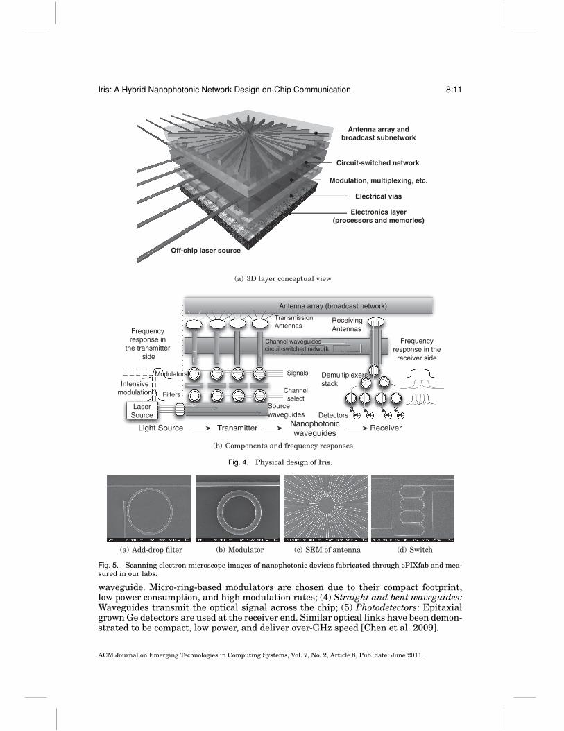
Figure 4(a) illustrates the proposed network architecture and many-core sys-tem integration. The proposed nanophotonic broadcast network consists of photonictransceivers, channel waveguides, photonic switches and a photonic broadcast antennaarray. The nanophotonic components are fabricated in separate silicon layers, and in-tegrated with the CMOS silicon die through a three-dimensional integration [Blacket al. 2006]. The design and fabrication of each layer can be optimized independently.
The optical path is composed of similar basic components for both the broadcast andcircuit-switched networks as shown in Figure 4(b). (1) Off-chip light source: A broad-band supercontinuum fiber laser light emitting at a power level of 4mW/nm [NKT2010] is chosen to provide cost-effective WDM laser power. (2) WDM filters: Passivemicro-ring filters are used to demultiplex the broadband light into wavelength chan-nels and deliver these channels to the system. We have fabricated several micro-ringsand they have been proven to be suitable candidates for filter design. Figure 5(a) showsa filter design fabricated and measured in our labs. (3) Modulators: Figure 5(b) showsa compact modulator design, with a 1.5μm radius ring resonator sitting alongside a
ACM Journal on Emerging Technologies in Computing Systems, Vol. 7, No. 2, Article 8, Pub. date: June 2011.
Iris: A Hybrid Nanophotonic Network Design on-Chip Communication 8:11
Electronics layer(processors and memories)
Electrical vias
Modulation, multiplexing, etc.
Circuit-switched network
Antenna array andbroadcast subnetwork
Off-chip laser source
(a) 3D layer conceptual view
Channel waveguides
circuit-switched network
Laser
Source
Signals
Channel
selectSource
waveguides
Filters
Modulators
Transmission
Antennas
Detectors
Demultiplexers
stack
Receiving
Antennas
Antenna array (broadcast network)
Intensive
modulation
Frequency
response in
the transmitter
side
Frequency
response in the
receiver side
Transmitter ReceiverNanophotonicwaveguides
Light Source
(b) Components and frequency responses
Fig. 4. Physical design of Iris.
(a) Add-drop filter (b) Modulator (c) SEM of antenna (d) Switch
Fig. 5. Scanning electron microscope images of nanophotonic devices fabricated through ePIXfab and mea-sured in our labs.
waveguide. Micro-ring-based modulators are chosen due to their compact footprint,low power consumption, and high modulation rates; (4) Straight and bent waveguides:Waveguides transmit the optical signal across the chip; (5) Photodetectors: Epitaxialgrown Ge detectors are used at the receiver end. Similar optical links have been demon-strated to be compact, low power, and deliver over-GHz speed [Chen et al. 2009].
ACM Journal on Emerging Technologies in Computing Systems, Vol. 7, No. 2, Article 8, Pub. date: June 2011.
8:12 Z. Li et al.
-80-75-70-65-60-55-50-45
1540 1545 1550 1555 1560 1565 1570 1575 1580
Pow
er
(dB
m)
Wavelength (nm)
Fig. 6. Measurement results of nanophotonic racetrack-based switch.
However, the broadcast and circuit-switched networks differ in the switching mech-anism. The broadcast network is based on an efficient antenna array, serving asan any-1-to-N fan-outs element. Figure 5(c) shows an antenna structure that wehave fabricated. In contrast, the circuit-switched network leverages optical switches.Figure 5(d) shows a third order stacked racetrack designed for switching optical pack-ets. Such design is chosen due to its wide bandwidth and small free spectral range asshown in the transmission graph in Figure 6.
Next, the physical design of the two subnetworks are discussed respectively.
5.1. Broadcast Subnetwork
The broadcast subnetwork scales a typical free space communication system design tothe micrometer length scale. It provides direct all-to-all connectivity for on-chip coresat low cost, low latency, and small power cost.
The antenna array is the key to efficient on-chip broadcasting since a single packetis sent once and received by all other communicating nodes. We have designed andfabricated the antenna structure [Zhou et al. 2010; Zhou and Filipovic 2010]. Initialmeasurement results are in good agreement with simulations. The antenna arrayconsists of dielectric-rod antennas [Kobayashi et al. 1981] in which the silicon ridgeguide’s width is tapered up from the nominal waveguiding value and then down tobelow cutoff. The structure of the waveguide taper determines the antenna radiationpattern. The apertures of the multiple antennas lie on the circumference of circle,approximately 3μm from each other, as shown in Figure 5(c). To increase the couplingefficiency among these antennas, a 500nm thick electro-optic polymer is coated on thesestructures.
The broadcast network design, as shown in Figure 2(b), provides low-latency trans-mission at high bandwidth. Light entering the chip is demultiplexed into 64 wave-lengths and modulated using micro-ring modulators. The modulated light is carried bya waveguide emanating toward the center of the chip where the antenna lies. Next, theoptical signal radiates through the antenna and is transmitted to all the other ports.Then the signal is carried through the waveguides to the rest of the cores withoutencountering any crossovers.
The broadcast network delivers high throughput and low latency. Electromagneticsimulation shows that the working range of our antenna structure extends from1350nm to 1650nm, completely covering the C+L bands (1530nm to 1625nm) [Zhouand Filipovic 2010]. As a broadband passive device, the operation of antenna array isnot susceptible to thermal variation. A large number of WDM channels can therefore besupported. The actual communication bandwidth equals the number of WDM channelstimes the bit rate per channel. The bit rate per channel could reach 4Gbps. Specifically,the propagation latency is composed of the following parts:
(1) TCLK→Q. Clock to Q propagation latency of the driving latch storing the informationto be transferred. TCLK→Q ≈ 31ps, assuming 32nm technology.
(2) Tm. Optical transmission of the modulator and its driver, Tm ≈ 36.3ps ([Chen et al.2007]).
ACM Journal on Emerging Technologies in Computing Systems, Vol. 7, No. 2, Article 8, Pub. date: June 2011.
Iris: A Hybrid Nanophotonic Network Design on-Chip Communication 8:13
(3) Tp. Time of flight. Tp = 0.75√
2×4.23 ×10−10s ≈ 149ps. We assume that the group index
of SOI waveguide is 4.2 [Dulkeith et al. 2006; Pergande and Wehrspohn 2010]. Thehorizontal and vertical dimension of the broadcast network is 0.75cm, which isthree quarters of the overall die side length. This assumes that the antenna arrayaccess points are placed in the corner of each tile.
(4) Tr. Receiver photodetector and amplifier delay, Tr ≈ 7.2ps [Chen et al. 2007].(5) Tsetup. Setup time of the latch receiving the signal, Tsetup = 19ps, assuming 32nm
technology.
The total delay is approximately 243ps. The bandwidth could reach 4Gbps per WDMchannel. Following the configuration described in Section 6, that is, 64 WDM channelsand 4Gbps per channel, the bandwidth of the broadcast network is 256Gbps.
Next, we focus on analyzing the power efficiency of our design. The following analysisshows that the proposed nanophotonic broadcast network is highly power efficient, andcan reliably operate at the milliwatt range per WDM channel at 4Gbps per channel. Todetermine the optical power budget for our broadcast network, we perform calculationsaccording to the loss budgeting method [Cox 2006]. First, we determine the minimumrequired signal power at the detector for a given bit error rate(BER) and system noise,taking into account the modulation loss. Then, the radiation in the broadcast network iscalculated to estimate the required input power according to Equation (1) in Section 2.3.Specifically, the optical receiver sensitivity is estimated to be -35dBm [Beausoleil et al.2008]. Table I gives a detailed account of the power loss of the different componentsalong the optical path. Antenna power loss is computed through 3D electro-magneticsimulations [HFSS; CST]. From full-wave simulations of the antenna structures, wecomputed an end-to-end transmission of 21.5dB for a 32-port antenna [Zhou andFilipovic 2010]. Using computer models we project the transmission to reach 25dB fora 64-port antenna used in our study. Hence, an input laser power of 0.86mW/channelis required at a BER of 10−12. For our 64-channel and 64-core system, a total power ofapproximately 3.6W is needed, which is quite low compared to electrical alternatives.The electrical power needed for the broadcast network is also minimized. Assumingthe same setup with a 20% activity factor, the aggregated receiver power consumptionis only 2.2W due to significant improvement in transceiver electrical circuitry power.In addition, during a broadcast operation, transmitters of a single sender are involved.The electrical power efficiency will improve along with CMOS technology.
5.2. Circuit-Switched Subnetwork
This section describes the physical design of the circuit-switched subnetwork in termsof performance and power.
The circuit-switched network is composed of channel waveguides and high-orderracetrack resonators, which function as links and switches, respectively. SOI-basedchannel waveguides can deliver unicast traffic at high throughput, with negligible loss.They are chosen to form the circuit-switched subnetwork, as depicted in Figure 2(a).In this design, they are arranged both horizontally and vertically to line up as amesh topology without bends or curves. As a result, the optical power loss has beensignificantly reduced. High-order racetrack resonators, controlled by electrical tuningsignals, sit at the waveguide crosses to form high bandwidth switches as shown inFigure 5(d). To save operating electrical power and area, they can operate multipleWDM channels simultaneously due to their wide passband width (shown in Figure 6).Such wide passband width is achieved by increasing the coupling efficiency and high-order filter design described in Chen et al. [2010]. In summary, regular network designminimizes optical loss, WDM can be leveraged to increase throughput at low operatingpower, and light-speed propagation shortens latency.
ACM Journal on Emerging Technologies in Computing Systems, Vol. 7, No. 2, Article 8, Pub. date: June 2011.
8:14 Z. Li et al.
Table I. Power Budget
Broadcast networkDevice Insertion loss Electrical power Number of devices
Grating coupler 1.6dB – 1[Vermeulen et al. 2009]
Demultiplexer at transmitters 1dB – –[Xiao et al. 2007]
Micro-ring modulator 2dB 5.9mW 4096with driver [Chen et al. 2009] [Lee et al. 2010]
Waveguide loss 3.79dB – –(2.82cm) [Selvaraja et al. 2009]
Antenna array 25dB – 1Demultiplexer at receivers 1dB – –
[Xiao et al. 2007]Receiver with – 2.76mW 4096
Ge photodetector [Zheng et al. 2010b]Total loss per wavelength 34.39dB – –
Channel-waveguide networkDevice Insertion loss Electrical power Number of devices
Grating coupler 1.6dB – 1[Vermeulen et al. 2009]
Demultiplexer at transmitters 1dB – –[Xiao et al. 2007]
Micro-ring modulator 2dB 5.9mW 4096with driver [Chen et al. 2009] [Lee et al. 2010]
Waveguide loss 5.36dB – –(4cm) [Selvaraja et al. 2009]
Waveguide crossings 0.045dB – 8/path[Popovic et al. 2007]
Switch loss 2dB 5.9mW 256[Chen et al. 2010] [Chen et al. 2009] [Lee et al. 2010]
Demultiplexer at receivers 1dB – –[Xiao et al. 2007]
Receiver with – 2.76mW 4096Ge photodetector [Zheng et al. 2010b]
Total loss per wavelength 13.32dB – –
Receiver sensitivity –35dbm [Beausoleil et al. 2008]
The network shows a superb performance. Throughput-wise, doped resonators canexhibit high operating speed [Chen et al. 2009]. In this study, we have assumed 4Gb/sper wavelength channel per link taking into account path propagation delay and electri-cal circuitry limitations at sender-receiver ends. By further assuming 64 WDM channelsetup, the 8-by-8 mesh network provides over 4Tb/s aggregated bisection bandwidth.Latency-wise, once the transmitting core gains access to the unicast network, thefull cache-line is transmitted without any non-deterministic delay due to contentionor routers. Since these messages are less sensitive to delay due to large serializa-tion latency, the arbitration delay has insignificant impact on system performance. Ananalysis of the subnetwork performance, especially throughput, will be presented inSection 6.
Next we analyze the power of the unicast network. The optical power loss is smallcompared to traditional photonic networks for two reasons: First, the unicast networkis free of bends; Second, due to the dimension order routing, the packet experienceonly one switch delay in worst case. Hence, the total insertion loss is small (13.32dBas shown in Table I). The electrical power of the network is dissipated mainly inmodulators, switches, and receivers. By leveraging the optical switch presented by
ACM Journal on Emerging Technologies in Computing Systems, Vol. 7, No. 2, Article 8, Pub. date: June 2011.
Iris: A Hybrid Nanophotonic Network Design on-Chip Communication 8:15
Table II. Configuration
Nanophotonic network in Iris Memory Hierarchy and Processors
Throughput per wavelength 4Gb/s L1 cache per core 64KB, 2-way 64-byte lineNumber of wavelengths 64 L2 cache per core 256KB, 16-way 128-byte line
aMemory access latency is composed of DRAM access time that is calculated by CACTI 6.5 tool [Murali-manohar et al. 2009] using 32nm high-performance technology, and chip-to-chip link latency assuming theDRAM is stacked via three dimensional hybrid integration technology.
[Chen et al. 2010], we can greatly reduce the overall number of devices and thus reduc-ing the overall power consumption. In this study we estimated the total electrical powerto be 7.4W, at an activity factor of 0.2, for the whole Iris network, including the broad-cast and channel-waveguide networks, following the power estimations presented inTable I.
6. SIMULATION RESULTS
In this section, we evaluate Iris, the proposed nanophotonic on-chip network, on a 64-core chip-multiprocessor. The performance and power efficiency of Iris are comparedagainst several recently proposed electrical and photonic alternatives. The simulationstudies demonstrate that the proposed design significantly reduces the power dissipa-tion and cache-network system latency for a set of typical scientific and commercialworkloads.
6.1. Evaluation Platform and Configuration
This simulation study targets a 64-core chip-multiprocessor design. The chip-multiprocessor occupies about 1cm2 silicon die. 3D integrated memory [Vantrease et al.2008] and chip-to-chip fiber connected memory [Batten et al. 2008] are assumed in thissetup. These technologies are likely to be widely adopted before on-chip nanophotonicnetworks are realized. Table II shows the configuration of the network and memoryhierarchy.
We have implemented a trace-driven cycle-accurate cache-network simulator, whichsimulates the activities of the memory hierarchy, the interconnection networks, andcache coherence protocol transactions. Network traffic traces are gathered using theM5 full-system simulator [Binkert et al. 2006] running several SPECOMP [Aslot et al.2001], SPLASH2 [SPLASH2] and ALPBench [Li et al. 2005] multithreaded bench-marks that we have, including ammp, applu, apsi, art, equake, fma3d, swim, wupwise,ocean, radix, cholesky, waternsq, lu, fft, fmm, and mpgenc. We also consider mem-ory access traces collected from three commercial server workloads: TPC-H, TPC-W [TheTransaction Processing Performance Council 2008], and SpecJBB [Standard Perfor-mance Evaluation Corporation 2008]. Each benchmark is spawned into 16 threads,which are distributed among the processor cores and executed concurrently. We con-solidated four benchmarks into the 64-core chip and executed them concurrently toemulate virtual machine run-time workload management.
The performance and power consumption of Iris is estimated based on recentnanophotonic device studies [Batten et al. 2008; Chen et al. 2009; Krishnamoorthyet al. 2010]. In Section 2.3 we presented an analysis of the basic components com-posing nanophotonic networks. Then more details were presented in Section 5 aboutIris’s broadcast and unicast networks. Performance analysis using state-of-the-art sil-icon photonic devices shows an approximately 243ps sender–receiver communication
ACM Journal on Emerging Technologies in Computing Systems, Vol. 7, No. 2, Article 8, Pub. date: June 2011.
8:16 Z. Li et al.
latency in the broadcast network. Therefore, the peak bit rate per wavelength channelis approximately 4Gbps, twice as fast as the electrical counterpart. We also consider a64 WDM channel setting in order to provide sufficient communication bandwidth andconcurrent transmission support. Future technology advances and proper pipeliningschemes can further improve the nanophotonic broadcast network speed.
6.2. Comparison of Iris and Alternatives
The performance and power efficiency of Iris are evaluated against the followingrecently-proposed electrical and photonic alternatives.
—E-mesh: a packet-switched electrical mesh network using virtual channel flow con-trols and supporting directory-based MESI protocol. It is equipped with recently-proposed latency-optimized two-pipeline-stage router design with speculative virtualchannel allocation [Mullins et al. 2004].
—P-mesh: a channel photonic waveguide based circuit-switched mesh network sup-porting directory protocol. It consists of a latency-optimized electrical network tosetup the photonic circuit-switched path. P-mesh is an approximation of a recently-proposed optical network design [Shacham et al. 2008].
—E-tree: a tree-based electrical network operated in one coherence domain, which isestablished from SUN Fireplane System Interconnect supporting the snoopy pro-tocol [Charlesworth 2001]. The address bus is implemented in a hierarchical treetopology with a fan-out of four at each node. The data bus is a packet-switchedelectrical mesh network.
—P-bus: A channel waveguide based photonic network supporting snoopy protocol[Kirman et al. 2006]. It consists of a set of snake-shape single-write multi-readwaveguides connecting on-chip processing units. The optical signal is broadcast alongeach waveguide.
—Corona: A serpentine multiwrite single-read waveguide-based crossbar net-work [Vantrease et al. 2008]. Each waveguide with WDM support is statically ded-icated to a single read node while other nodes compete by cycling tokens. Networkperformance is limited by the token cycling that requires 8 clock cycles per roundtrip, and by the directory coherence protocol.
In this study, E-mesh and E-tree are used to quantify the overall performance im-provement and power savings of the proposed nanophotonic solution over existingelectrical alternatives. Photonic alternatives P-mesh, P-bus, and Corona are used toevaluate the latency and power impact of Iris over recently published nanophotonicnetworks.
In addition, in order to evaluate the throughput and power trade-offs, the circuit-switched photonic subnetwork in Iris is replaced with electrical packet-switched andcircuit-switched mesh networks as the following two alternatives.
—Packet. It is a hybrid network consisting of a broadcast photonic subnetwork andan electrical packet-switched mesh subnetwork. Protocol messages will be sent viabroadcast network like in Iris, but the large data packets will be sent via the electricalsubnetwork with hop-by-hop arbitration and buffering. Packet is evaluated againstIris’ circuit-switched photonic subnetwork in terms of the throughput and powerefficiency.
—Circuit. Similar to Packet, it is a hybrid electrical-photonic interconnect except thatthe electrical network in Circuit is circuit switched. The circuit switch path setupis scheduled by broadcast network similar to Iris. This configuration is to show howphotonic interconnect outperform electrical alternatives by providing low latencyand high throughput.
ACM Journal on Emerging Technologies in Computing Systems, Vol. 7, No. 2, Article 8, Pub. date: June 2011.
Iris: A Hybrid Nanophotonic Network Design on-Chip Communication 8:17
0
5
10
15
20
Iris
Cir
cuit
Pac
ket
E−
mes
hP
−m
esh
P−
Bus
E−
Tre
eC
oron
a
Iris
Cir
cuit
Pac
ket
E−
mes
hP
−m
esh
P−
Bus
E−
Tre
eC
oron
a
Iris
Cir
cuit
Pac
ket
E−
mes
hP
−m
esh
P−
Bus
E−
Tre
eC
oron
a
Iris
Cir
cuit
Pac
ket
E−
mes
hP
−m
esh
P−
Bus
E−
Tre
eC
oron
a
Iris
Cir
cuit
Pac
ket
E−
mes
hP
−m
esh
P−
Bus
E−
Tre
eC
oron
a
Iris
Cir
cuit
Pac
ket
E−
mes
hP
−m
esh
P−
Bus
E−
Tre
eC
oron
a
Iris
Cir
cuit
Pac
ket
E−
mes
hP
−m
esh
P−
Bus
E−
Tre
eC
oron
a
Iris
Cir
cuit
Pac
ket
E−
mes
hP
−m
esh
P−
Bus
E−
Tre
eC
oron
a
Iris
Cir
cuit
Pac
ket
E−
mes
hP
−m
esh
P−
Bus
E−
Tre
eC
oron
a
Iris
Cir
cuit
Pac
ket
E−
mes
hP
−m
esh
P−
Bus
E−
Tre
eC
oron
a
Iris
Cir
cuit
Pac
ket
E−
mes
hP
−m
esh
P−
Bus
E−
Tre
eC
oron
a
Iris
Cir
cuit
Pac
ket
E−
mes
hP
−m
esh
P−
Bus
E−
Tre
eC
oron
a
Pow
er (
W)
apsi
−eq
uake
−fm
a3d−
appl
u
fft−
lu−
mpg
enc−
ocea
n
radi
x−w
ater
nsq
−lu
−m
pgen
c
ocea
n−ch
oles
ky−
fft−
wat
erns
q
amm
p−eq
uake
−sw
im−
equa
ke
fma3
d−ap
si−
amm
p−w
upw
ise
fft−
lu−
mpg
enc−
chol
esky
wat
erns
q−lu
−m
pgen
c−ra
dix
amm
p−fm
a3d
−w
upw
ise−
swim
equa
ke−
fma3
d−
apsi
−am
mp
fft−
mpg
enc
−oc
ean−
chol
esky
spec
jbb−
tpch
−tp
cw−
lu
Optical sourceRouters and linksElectro−optical
Fig. 7. Power consumption comparison.
6.3. Power Efficiency Evaluation
Figure 7 shows the on-chip power dissipation breakdown of Iris and the other sevenalternatives. The electrical network power consumption of each of the alternatives iscalculated by ORION2.0 [Kahng et al. 2009] at 32nm technology. The power consump-tion of the electrical network is contributed by routers and link circuitry (labeled as“Routers and links”). The power dissipation of the nanophotonic network is contributedby light source (labeled as “Optical source”), and electrical transmitter, receiver andswitch power for unicasting/broadcasting (labeled as “Electro-optical”).
This study shows that Iris is the most power efficient on-chip interconnect solution.Compared to electrical alternatives E-mesh and E-tree, Iris reduces the average powerconsumption by 19.5% and 50.6%, respectively. This shows that global electrical in-terconnect is not power-efficient for on-chip communication, especially for chip-scalebroadcast. Compared to photonic alternatives P-mesh, P-bus, and Corona, Iris alsoreduces the average power consumption by 20.3%, 92.7%, and 1.8%, respectively. InP-mesh, power overhead mainly comes from the non-scalable static-power consumptionof the electrical network used to set up the bufferless photonic link paths. In P-bus,photonic splitters are introduced along the channel waveguides for broadcasting. Aseach node along the waveguide taps the same portion of the incoming optical power, therequired optical power is exponentially proportional to the number of cores. In Corona,serpentine waveguides are long and introduce excessive insertion loss. To minimizethe waveguide propagation and bending loss, the optical access points of neighboringcores are placed close to each other, introducing increased electrical dissipation fromthe longer electrical wires.
On the other hand, Packet and Circuit does not show power benefits because the majortraffic load: data packets are still transferred via electrical network. The removal ofsmall protocol messages does not lead to significant power reduction. Compared toPacket and Circuit, Iris reduces the overall network power consumption by 45.3%and 33.1%.
As technology scales further, the power efficiency of nanophotonic devices and compo-nents is expected to improve. The power consumption of the electrical network, on theother hand, is expected to increase. Therefore, using nanophotonic on-chip interconnect
ACM Journal on Emerging Technologies in Computing Systems, Vol. 7, No. 2, Article 8, Pub. date: June 2011.
8:18 Z. Li et al.
0
20
40
60
80
100
120
Iris
Cir
cuit
Pac
ket
E−
mes
hP
−m
esh
P−
bus
E−
tree
Cor
ona
Iris
Cir
cuit
Pac
ket
E−
mes
hP
−m
esh
P−
bus
E−
tree
Cor
ona
Iris
Cir
cuit
Pac
ket
E−
mes
hP
−m
esh
P−
bus
E−
tree
Cor
ona
Iris
Cir
cuit
Pac
ket
E−
mes
hP
−m
esh
P−
bus
E−
tree
Cor
ona
Iris
Cir
cuit
Pac
ket
E−
mes
hP
−m
esh
P−
bus
E−
tree
Cor
ona
Iris
Cir
cuit
Pac
ket
E−
mes
hP
−m
esh
P−
bus
E−
tree
Cor
ona
Iris
Cir
cuit
Pac
ket
E−
mes
hP
−m
esh
P−
bus
E−
tree
Cor
ona
Iris
Cir
cuit
Pac
ket
E−
mes
hP
−m
esh
P−
bus
E−
tree
Cor
ona
Iris
Cir
cuit
Pac
ket
E−
mes
hP
−m
esh
P−
bus
E−
tree
Cor
ona
Iris
Cir
cuit
Pac
ket
E−
mes
hP
−m
esh
P−
bus
E−
tree
Cor
ona
Iris
Cir
cuit
Pac
ket
E−
mes
hP
−m
esh
P−
bus
E−
tree
Cor
ona
Iris
Cir
cuit
Pac
ket
E−
mes
hP
−m
esh
P−
bus
E−
tree
Cor
ona
L2
cach
e m
iss
late
ncy
(cyc
les)
apsi
−eq
uake
−fm
a3d−
appl
u
fft−
lu−
mpg
enc−
ocea
n
radi
x−w
ater
nsq
−lu
−m
pgen
c
ocea
n−ch
oles
ky−
fft−
wat
erns
q
amm
p−eq
uake
−sw
im−
equa
ke
fma3
d−ap
si−
amm
p−w
upw
ise
fft−
lu−
mpg
enc−
chol
esky
wat
erns
q−lu
−m
pgen
c−ra
dix
amm
p−fm
a3d
−w
upw
ise−
swim
equa
ke−
fma3
d−
apsi
−am
mp
fft−
mpg
enc
−oc
ean−
chol
esky
spec
jbb−
tpch
−tp
cw−
lu
MemoryResponseProtocolRequest
Fig. 8. Performance comparison: average local L2 miss latency.
becomes increasingly power beneficial. More specifically, Iris shows better power effi-ciency and is expected to dominate in future technologies.
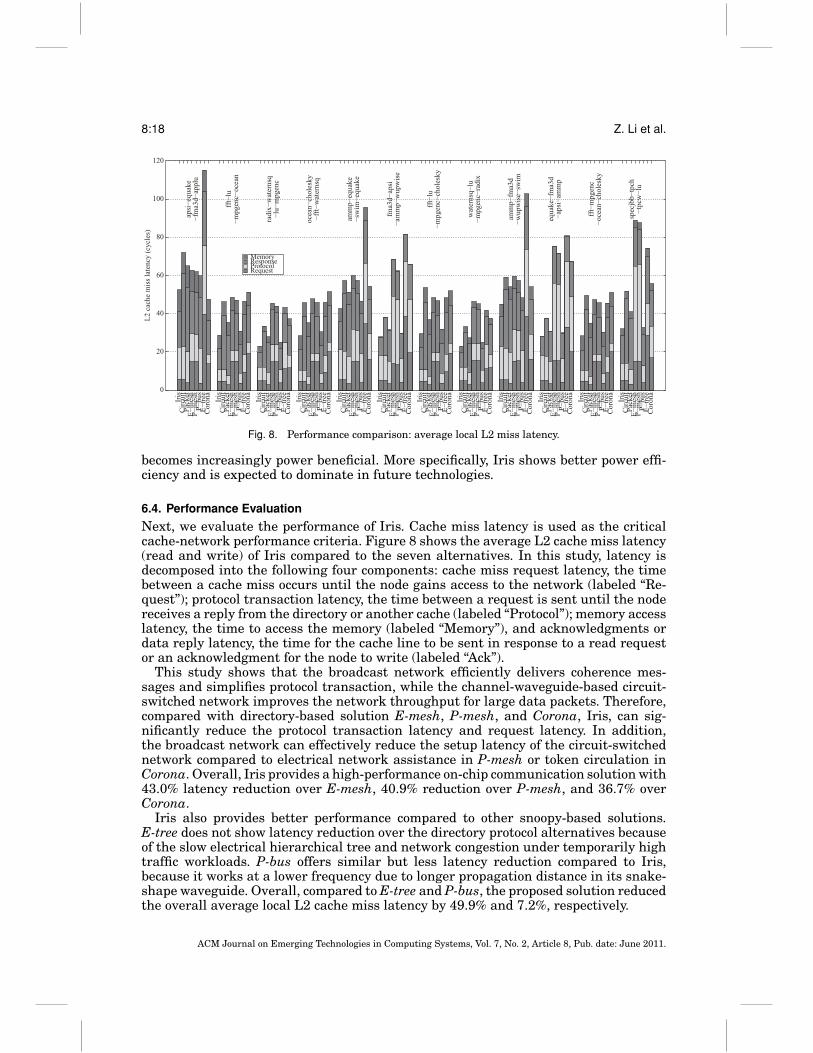
6.4. Performance Evaluation
Next, we evaluate the performance of Iris. Cache miss latency is used as the criticalcache-network performance criteria. Figure 8 shows the average L2 cache miss latency(read and write) of Iris compared to the seven alternatives. In this study, latency isdecomposed into the following four components: cache miss request latency, the timebetween a cache miss occurs until the node gains access to the network (labeled “Re-quest”); protocol transaction latency, the time between a request is sent until the nodereceives a reply from the directory or another cache (labeled “Protocol”); memory accesslatency, the time to access the memory (labeled “Memory”), and acknowledgments ordata reply latency, the time for the cache line to be sent in response to a read requestor an acknowledgment for the node to write (labeled “Ack”).
This study shows that the broadcast network efficiently delivers coherence mes-sages and simplifies protocol transaction, while the channel-waveguide-based circuit-switched network improves the network throughput for large data packets. Therefore,compared with directory-based solution E-mesh, P-mesh, and Corona, Iris, can sig-nificantly reduce the protocol transaction latency and request latency. In addition,the broadcast network can effectively reduce the setup latency of the circuit-switchednetwork compared to electrical network assistance in P-mesh or token circulation inCorona. Overall, Iris provides a high-performance on-chip communication solution with43.0% latency reduction over E-mesh, 40.9% reduction over P-mesh, and 36.7% overCorona.
Iris also provides better performance compared to other snoopy-based solutions.E-tree does not show latency reduction over the directory protocol alternatives becauseof the slow electrical hierarchical tree and network congestion under temporarily hightraffic workloads. P-bus offers similar but less latency reduction compared to Iris,because it works at a lower frequency due to longer propagation distance in its snake-shape waveguide. Overall, compared to E-tree and P-bus, the proposed solution reducedthe overall average local L2 cache miss latency by 49.9% and 7.2%, respectively.
ACM Journal on Emerging Technologies in Computing Systems, Vol. 7, No. 2, Article 8, Pub. date: June 2011.
Iris: A Hybrid Nanophotonic Network Design on-Chip Communication 8:19
20
40
60
90
120
0.01 0.05 0.1 0.2
Cohere
nce
pro
tocol dela
y
(cycle
s)
Cache miss injection rate (misses per cycle)
IrisCircuitPacket
Fig. 9. Throughput analysis.
Iris also provides power efficient, high performance solutions for data packets.Equipped with the same antenna-array-based subnetwork, the overall network latencyin Iris shows 32.7% reduction over Circuit and 17.2% reduction over Packet.
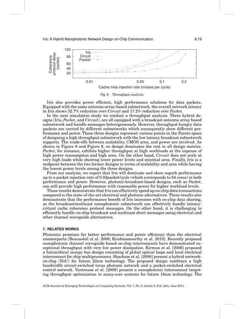
In the next simulation study we conduct a throughput analysis. Three hybrid de-signs (Iris, Packet, and Circuit), are all equipped with a broadcast antenna array basedsubnetwork and handle messages heterogeneously. However, throughput-hungry datapackets are carried by different subnetworks which consequently show different per-formance and power. These three designs represent various points in the Pareto spaceof designing a high throughput subnetwork with the low latency broadcast subnetworksupports. The trade-offs between scalability, CMOS area, and power are involved. Asshown in Figure 8 and Figure 9, no design dominates the rest in all design metrics.Packet, for instance, exhibits higher throughput at high workloads at the expense ofhigh power consumption and high area. On the other hand, Circuit does not scale atvery high loads while showing lower power levels and minimal area. Finally, Iris is amidpoint between the two former designs in terms of scalability and area while havingthe lowest power levels among the three designs.
From our analysis, we expect that Iris will dominate and show superb performanceup to a packet injection rate of 0.02packet/cycle (which corresponds to 64 cores) in bothperformance and power. However, photonic-broadcast-based designs, such as Packet,can still provide high performance with reasonable power for higher workload levels.
These results demonstrate that Iris can effectively speed up on-chip data transactionscompared to the state-of-the-art electrical and photonic alternatives. These results alsodemonstrate that the performance benefit of Iris increases with on-chip data sharing,as the broadcast/multicast nanophotonic subnetwork can effectively handle latency-critical cache coherence protocol messages. On the other hand, it is challenging toefficiently handle on-chip broadcast and multicast short messages using electrical andother channel waveguide alternatives.
7. RELATED WORKS
Photonics promises far better performance and power efficiency than the electricalcounterparts [Beausoleil et al. 2008; Krishnamoorthy et al. 2010]. Recently proposednanophotonic channel waveguide based on-chip interconnects have demonstrated ex-ceptional throughput with very low power dissipation. Kirman et al. [2006] proposeda hierarchical snoopy bus design consisting of global optical loops and local electricalinterconnect for chip multiprocessors. Shacham et al. [2008] present a hybrid network-on-chip (NoC) for future 22nm technology. The proposed design combines a highbandwidth circuit-switched torus photonic network and a packet-switched electricalcontrol network. Vantrease et al. [2008] present a nanophotonic interconnect target-ing throughput optimization in many-core systems for future 16nm technology. The
ACM Journal on Emerging Technologies in Computing Systems, Vol. 7, No. 2, Article 8, Pub. date: June 2011.
8:20 Z. Li et al.
proposed design leverages WDM and a novel all-optical token arbitration scheme. Thisarbitration scheme is further investigated in Vantrease et al. [2009]. Batten et al. [2008]proposed using monolithic silicon photonics for many core processor-to-DRAM intercon-nect. Joshi et al. [2009] proposed a clos topology using photonic interconnect for globalon-chip communication. Pan et al. [2009] proposed Firefly, a hierarchical cluster-basedtopology. The inter-cluster optical crossbar is a combination of 1) single-read-multi-write bus similar to Corona [Vantrease et al. 2008] and 2) single-write-multi-read bussimilar to Kirman Bus [Kirman et al. 2006]. Firefly improves the network throughputby efficient sharing and favors local communication. Cianchetti et al. [2009] proposeda router in an on-chip optical network, called Phastlane. The router can leverage elec-trical buffers and optical nonblocking links. Miller et al. [2009] proposed ATAC, asnake-shape channel waveguide based broadcast on-chip interconnect architecture, tooptimize directory-based cache coherence protocol. Xue et al. [2010] proposed bondinglaser sources and micromirrors on top of CMOS chip to provide free space optical inter-connect. Researchers in Oracle proposed “macrochip”, a multichip system interconnectsolution leveraging silicon photonic technology [Zheng et al. 2008; Koka et al. 2010].
8. CONCLUSION
Many-core on-chip systems call for power-efficient, high-performance on-chip com-munication solutions. In this work, we study the electrical and photonic on-chip in-terconnect in detail and propose Iris, a nanophotonic on-chip network, which con-sists of a low-latency antenna-array-based WDM broadcast/multicast subnetwork,and a throughput-optimized channel-waveguide based circuit-switching subnetwork.The proposed design provides power-efficient support for both latency-critical andthroughput-critical on-chip communication traffic of many-core systems. Simulationresults show that, compared with other recently proposed electrical mesh, electricaltree, photonic mesh, photonic bus and photonic crossbar alternatives, Iris improvesperformance by 43.0%, 49.9%, 40.9%, 7.2%, and 36.7%, and power efficiency by 19.5%,50.6%, 20.3%, 92.7%, and 1.8%, respectively.
REFERENCES
ASLOT, V., DOMEIKA, M., EIGENMANN, R., GAERTNER, G., JONES, W. B., AND PARADY, B. 2001. SPEComp: A newbenchmark suite for measuring parallel computer performance. In Proceedings of the Workshop onOpenMP Applications and Tools. 1–10.
BATTEN, C., JOSHI, A., ORCUTT, J., KHILO, A., MOSS, B., HOLZWARTH, C., POPOVIC, M., LI, H., SMITH, H., HOYT,J., KARTNER, F., RAM, R., STOJANOVIC, V., AND ASANOVIC, K. 2008. Building manycore processor-to-DRAMnetworks with monolithic silicon photonics. In Proceedings of the IEEE Symposium on High PerformanceInterconnects. 21–30.
BEAUSOLEIL, R. G., KUEKES, P. J., SNIDER, G. S., WANG, S.-Y., AND WILLIAMS, R. S. 2008. Nanoelectronic andnanophotonic interconnect. Proc. IEEE 96, 2, 230–247.
BINKERT, N. L., DRESLINSKI, R. G., HSU, L. R., LIM, K. T., SAIDI, A. G., AND REINHARDT, S. K. 2006. The M5simulator: Modeling networked systems. IEEE Micro 26, 4, 52–60.
BLACK, B., ANNAVARAM, M., BREKELBAUM, N., DEVALE, J., JIANG, L., LOH, G. H., MCCAULE, D., MORROW, P., NELSON,D. W., PANTUSO, D., REED, P., RUPLEY, J., SHANKAR, S., SHEN, J., AND WEBB, C. 2006. Die stacking (3D)microarchitecture. In Proceedings of the International Symposium on Microarchitecture. 469–479.
CHARLESWORTH, A. 2001. The SUN fire plane system interconnect. In Proceedings of the SupercomputingConference. 7.
CHEN, G., CHEN, H., HAURYLAU, M., NELSON, N. A., ALBONESI, D. H., FAUCHET, P. M., AND FRIEDMAN, E. G. 2007.Predictions of CMOS compatible on-chip optical interconnect. Integr. VLSI J. 40, 4, 434–446.
CHEN, L., PRESTON, K., MANIPATRUNI, S., AND LIPSON, M. 2009. Integrated GHz silicon photonic interconnectwith micrometer-scale modulators and detectors. Opt. Express 17, 17, 15248–15256.
CHEN, X., MOHAMED, M., SCHWARTZ, B., LI, Z., SHANG, L., AND MICKELSON, A. 2010. Racetrack filters for nanopho-tonic on-chip networks. In Proceedings of the Integrated Photonics Research, Silicon and Nano Photonics(IPR).
ACM Journal on Emerging Technologies in Computing Systems, Vol. 7, No. 2, Article 8, Pub. date: June 2011.
Iris: A Hybrid Nanophotonic Network Design on-Chip Communication 8:21
CIANCHETTI, M. J., KEREKES, J. C., AND ALBONESI, D. H. 2009. Phastlane: a rapid transit optical routing network.In Proceedings of the International Symposium on Computer Architecture. 441–450.
COX, C. H. 2006. Analog Optical Links: Theory and Practice. Cambridge University Press.CST. Complete technology for 3D electromagnetic simulation. http://www.cst.com.DULKEITH, E., XIA, F., SCHARES, L., GREEN, W. M. J., AND VLASOV, Y A. 2006. Group index and group velocity
dispersion in silicon-on-insulator photonic wires. Opt. Express 14, 9, 3853–3863.ePIXfab 2008. EPIXFAB 2008. ePIXfab website. http://www.epixfab.eu/.GRATZ, P., KIM, C., SANKARALINGAM, K., HANSON, H., SHIVAKUMAR, P., KECKLER, S. W., AND BURGER, D. 2007.
On-chip interconnection networks of the TRIPS chip. IEEE Micro 27, 5, 41–50.HFSS. High frequency structural simulator. http://www.ansoft.com/products/hf/hfss/.HOSKOTE, Y, VANGAL, S., SINGH, A., BORKAR, N., AND BORKAR, S. 2007. A 5-GHz mesh interconnect for a teraflops
G., PAILET, F., JAIN, S., JACOB, T., YADA, S., MARELLA, S., SALIHUNDAM, P., ERRAGUNTLA, V, KONOW, M., RIEPEN,M., DROEGE, G., LINDEMANN, J., GRIES, M., APEL, T., HENRISS, K., LUND-LARSEN, T., STEIBL, S., BORKAR, S., DE,V, WIJNGAART, R. V. D., AND MATTSON, T. 2010. A 48-core IA-32 message-passing processor with DVFS in45nm CMOS. In Proceedings of the International Solid-State Circuits Conference. 108–109.
ITRS 2008. International Technology Roadmap for Semiconductors. http://public.itrs.net/.JERGER, N. E., PEH, L.-S., AND LIPASTI, M. 2008. Virtual circuit tree multicasting: A case for on-chip hardware
multicast support. In Proceedings of the International Symposium on Computer Architecture.JOSHI, A., BATTEN, C., KWON, Y.-J., BEAMER, S., SHAMIM, I., ASANOVIC, K., AND STOJANOVIC, V 2009. Silicon-photonic
clos networks for global on-chip communication. In Proceedings of the International Symposium onNetworks-on-Chip. 124–133.
KAHNG, A., LI, B., PEH, L.-S., AND SAMADI, K. 2009. ORION 2.0: A fast and accurate NoC power and area modelfor early-stage design space exploration. In Proceedings of the Design, Automation & Test in EuropeConference. 423–428.
KIRMAN, N., KIRMAN, M., DOKANIA, R. K., MARTINEZ, J. F., APSEL, A. B., WATKINS, M. A., AND ALBONESI, D. H.2006. Leveraging optical technology in future bus-based chip multiprocessors. In Proceedings of theInternational Symposium on Microarchitecture. 492–503.
KOBAYASHI, S., LAMPE, R., MITTRA, R., AND RAY, S. 1981. Dielectric rod leaky-wave antennas for millimeter-waveapplications. IEEE Trans.Antennas Propag. 29, 5, 822–824.
KOESTER, S., SCHOW, C., SCHARES, L., DEHLINGER, G., SCHAUB, J., DOANY, F., AND JOHN, R. 2007. Ge-on-SOI-Detector/Si-CMOS-Amplifier receivers for high-performance opticalcommunication applications. J.Lightwave Technol. 25, 1, 46–57.
KOKA, P., MCCRACKEN, M. O., SCHWETMAN, H., ZHENG, X., HO, R., AND KRISHNAMOORTHY, A. V. 2010. Silicon-photonic network architectures for scalable, power-efficient multi-chip systems. In Proceedings of theInternational Symposium on Computer Architecture. 117–128.
KRISHNAMOORTHY, A. V, GOOSSEN, K. W., JAN, W., ZHENG, X., HO, R., LI, G., ROZIER, R., LIU, F., PATIL, D., LEXAU,J., SCHWETMAN, H., FENG, D., ASGHARI, M., PINGUET, T., AND CUNNINGHAM, J. E. 2010. Progress in low-powerswitched optical interconnects. IEEE J. Select. Top. Quantum Electron.
LEE, B. G., CAMPENHOUT, J. V., RYLYAKOV, A. V., SCHOW, C. L., GREEN, W. M., ASSEFA, S., YANG, M., DOANY, F. E.,JAHNES, C. V., JOHN, R. A., KASH, J. A., AND VLAS, Y A. 2010. Broadband silicon photonic switch integratedwith CMOS drive electronics. In Proceedings of the Conference on Lasers and Electro-Optics. Proceedingsof the Conference on Lasers and Electro-Optics.
LI, M.-L., SASANKA, R., ADVE, S. V., CHEN, Y-K., AND DEBES, E. 2005. The ALPbench benchmark suite for complexmultimedia applications. In Proceedings of the International Symposium on Workload Characterization.34–35.
LITTLE, B. E., HAUS, H. A., FORESI, J. S., KIMMERLING, L., IPPEN, E. P., AND RIPIN, D. J. 1998. Wavelength switchingand routing using absorption and resonance. IEEE Photon. Techn. Lett. 10, 6, 816–818.
MARTIN, M., HILL, M., AND WOOD, D. 2003. Token coherence: decoupling performance and correctness. InProceedings of the International Symposium on Computer Architecture. 182–193.
MILLER, J., PSOTA, J., KURIAN, G., BECKMANN, N., EASTEP, J., LIU, J., BEALS, M., MICHEL, J., KIMERLING, L., AND
AGARWAL, A. 2009. ATAC: A manycore processor with on-chip optical network. Tech. rep., MassachusettsInstitute of Technology.
MULLINS, R., WEST, A., AND MOORE, S. 2004. Low-latency virtual-channel routers for on-chip networks. InProceedings of the International Symposium on Computer Architecture. 188–197.
MURALIMANOHAR, N., BALASUBRAMONIAN, R., AND JOUPPI, N. P. 2009. CACTI 6.0: A tool to model large caches.Tech. rep., HP Laboratories.
ACM Journal on Emerging Technologies in Computing Systems, Vol. 7, No. 2, Article 8, Pub. date: June 2011.
8:22 Z. Li et al.
NKT 2010. NKT photonics website. http://www.nktphotonics.com/.PAN, Y, KUMAR, P., KIM, J., MEMIK, G., ZHANG, Y, AND CHOUDHARY, A. 2009. Firefly: illuminating future network-
on-chip with nanophotonics. In Proceedings of the International Symposium on Computer Architecture.429–440.
PERGANDE, D. AND WEHRSPOHN, R. B. 2010. Losses and group index dispersion in insulatoron-silicon-on-insulator ridgewaveguides. Opt. Express 18, 5, 4590–4600.
POPOVIC, M., IPPEN, E., AND KARTNER, F. 2007. Low-loss bloch waves in open structures and highly compact,efficient si waveguide-crossing arrays. In Proceedings of the Annual Meeting of the IEEE Lasers andElectro-Optics Society (LEOS).
SAHNI, S., LUO, X., LIU, J., HONG XIE, Y, AND YABLONOVITCH, E. 2008. Junction field-effect transistor-basedgermanium photodetector on silicon-on-insulator. Opt. Lett. 33, 10, 1138–1140.
SELVARAJA, S. K., SLEECKX, E., SCHAEKERS, M., BOGAERTS, W., THOURHOUT, D. V., DUMON, P., AND BAETS, R. 2009.Low-loss amorphous silicon-on-insulator technology for photonic integrated circuitry. Opt. Comm. 282,9, 1767–1770.
SHACHAM, A., BERGMAN, K., AND CARLONI, L. 2008. Photonic networks-on-chip for future generations of chipmultiprocessors. IEEE Trans. Comput. 57, 9, 1246–1260.
SPLASH2. SPLASH2 website. http://www-flash.stanford.edulapps/SPLASH/.Standard Performance Evaluation Corporation 2008. Java business benchmark. http://www.spec.org.TRANSACTION PROCESSING PERFORMANCE COUNCIL 2008. Transaction processing and database benchmarks.
http://www.tpc.org.VANTREASE, D., BINKERT, N., SCHREIBER, R., AND LIPASTI, M. H. 2009. Light speed arbitration and flow control
for nanophotonic interconnects. In Proceedings of the International Symposium on Microarchitecture.VANTREASE, D., SCHREIBER, R., MONCHIERO, M., MCLAREN, M., JOUPPI, N. P., FIORENTINO, M., DAVIS, A., BINKERT,
N., BEAUSOLEIL, R. G., AND AHN, J. H. 2008. Corona: System implications of emerging nanophotonictechnology. In Proceedings of the International Symposium on Computer Architecture. 153–164.
VERMEULEN, D., SELVARAJA, S., VERHEYEN, P., LEPAGE, G., BOGAERTS, W., AND ROELKENS, G. 2009. High-efficiencysilicon-on-insulator fiber-to-chip grating couplers using a silicon overlay. In Proceedings of the 6th IEEEInternational Conference on Group N Photonics.
VLASOV, Y AND MCNAB, S. 2004. Losses in single-mode silicon-on-insulator strip waveguides and bends. Opt.Express 12, 8, 1622–1631.
XIAO, S., KHAN, M., SHEN, H., AND QI, M. 2007. Low-loss ultra-compact soi microring add-drop filters. InFrontiers in Optics. Optical Society of America, PDP D6.
XUE, J., GARG, A., CIFTCIOGLU, B., HU, J., WANG, S., SAVIDIS, I., JAIN, M., BERMAN, R., LIU, P., HUANG, M., WU, H.,FRIEDMAN, E., WICKS, G., AND MOORE, D. 2010. An intra-chip free-space optical interconnect. In Proceedingsof the International Symposium on Computer Architecture. 94–105.
ZHENG, X., KOKA, P., SCHWETMAN, H., LEXAU, J., HO, R., CUNNINGHAM, J., AND KRISHNAMOORTHY, A. 2008. Siliconphotonic wdm point-to-point network for multi-chip processor interconnects. In Proceedings of the 5thIEEE International Conference on Group IV Photonics. 380–382.
ZHENG, X., LEXAU, J., LUO, Y, THACKER, H., PINGUET, T., MEKIS, A., LI, G., SRI, J., AMBERG, P., PINCKNEY, N., RAJ,K., HO, R., CUNNINGHAM, J. E., AND KRISHNAMOORTHY, A. V. 2010a. Ultra-low-energy all-CMOS modulatorintegrated with driver. Opt. Express 18, 3, 3059–3070.
ZHENG, X., LIU, F., PATIL, D., THACKER, H., LUO, Y, PINGUET, T., MEKIS, A., YAO, J., LI, G., SRI, J., RAJ, K., LEXAU,J., ALON, E., HO, R., CUNNINGHAM, J. E., AND KRISHNAMOORTHY, A. V. 2010b. A sub-picojoule-per-bit CMOSphotonic receiver for densely integrated systems. Opt. Express 18, 1, 204–211.
ZHOU, H. AND FILIPOVIC, D. S. 2010. Optical dielectric rod antenna for on-chip communications. In Proceedingsof the IEEE Antennas and Propagation Symposium. 1–4.
ZHOU, H., LI, Z., SHANG, L., MICKELSON, A., AND FILIPOVIC, D. S. 2010. On-chip wireless optical broadcastinterconnection network. J. Lightwave Techn. 28, 24, 3569–3577.
Received August 2010; revised January 2011; accepted March 2011
ACM Journal on Emerging Technologies in Computing Systems, Vol. 7, No. 2, Article 8, Pub. date: June 2011.