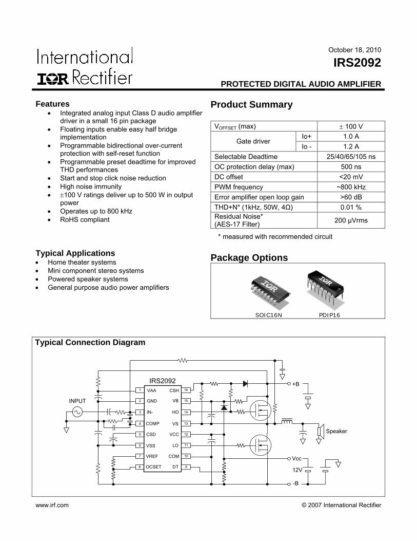
Description The IRS2092 is a high voltage, high performance Class D audio amplifier driver with PWM modulator and protection. In conjunction with two external MOSFET and a few external components, a complete Class D audio amplifier with protection can be realized. International Rectifier’s proprietary noise isolation technology allows high current gate drive stage and high speed low noise error amplifier reside on a single small silicon die. Open elements of PWM modulator section allow flexible PWM topology implementation.
Machine Model Class B (per JEDEC standard JESD22-A114D)
Human Body Model Class 2 (per EIA/JEDEC standard EIA/JESD22-A115-A) ESD
Charged Device Model Class IV (per JEDEC standard JESD22-C101C)
IC Latch-Up Test Class I, Level A (per JESD78A)
RoHS Compliant Yes † Qualification standards can be found at International Rectifier’s web site http://www.irf.com/ †† Higher qualification ratings may be available should the user have such requirements. Please contact your
International Rectifier sales representative for further information. ††† Higher MSL ratings may be available for the specific package types listed here. Please contact your
International Rectifier sales representative for further information.
Absolute Maximum Ratings Absolute Maximum Ratings indicate sustained limits beyond which damage to the device may occur. All voltage parameters are absolute voltages referenced to COM; all currents are defined positive into any lead. The Thermal Resistance and Power Dissipation ratings are measured under board mounted and still air conditions. Symbol Definition Min Max Units
VB High side floating supply voltage -0.3 220 VS High side floating supply voltage (Note2) VB -20 VB +0.3 VHO High side floating output voltage VS -0.3 VB +0.3 VCSH CSH pin input voltage VS -0.3 VB +0.3 VCC Low side fixed supply voltage (Note2) -0.3 20 VLO Low side output voltage -0.3 Vcc+0.3 VAA Floating input positive supply voltage (Note2) (See IAAZ) 210
VSS Floating input negative supply voltage (Note2) -1 (See ISSZ) GND +0.3
VGND Floating input supply ground voltage VSS -0.3
(See ISSZ) VAA +0.3 (See IAAZ)
V
IIN- Inverting input current (Note1) --- ±3 mA VCSD SD pin input voltage VSS -0.3 VAA +0.3
VCOMP COMP pin input voltage VSS -0.3 VAA +0.3 VDT DT pin input voltage -0.3 VCC +0.3
VOCSET OCSET pin input voltage -0.3 VCC+0.3
V
IAAZ Floating input positive supply zener clamp current (Note2) --- 20 ISSZ Floating input negative supply zener clamp current (Note2) --- 20 ICCZ Low side supply zener clamp current (Note3) --- 10 IBSZ Floating supply zener clamp current (Note3) --- 10 IOREF Reference output current --- 5
mA
dVS/dt Allowable Vs voltage slew rate --- 50 V/ns dVSS/dt Allowable Vss voltage slew rate (Note3) --- 50 V/ms
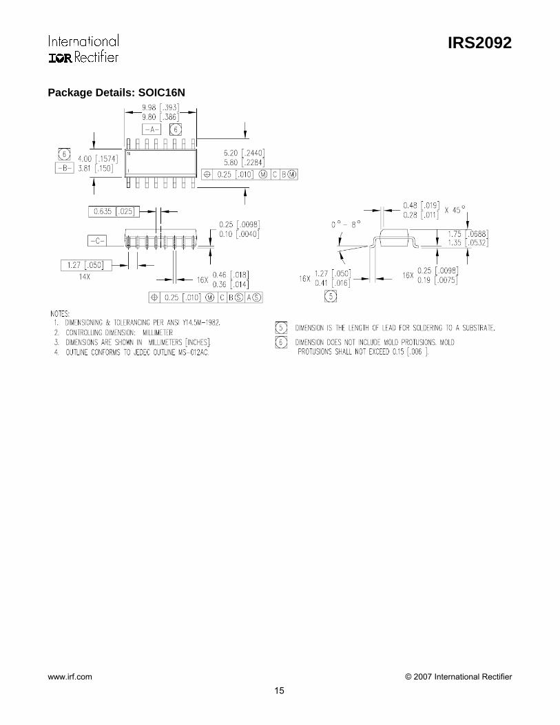
SOIC16N --- 1.0 Pd Maximum power dissipation @ TA ≤ +25°C
DIP16 --- 1.6 W
SOIC16N --- 115 RthJA Thermal resistance, Junction to ambient
DIP16 --- 75 °C/W
TJ Junction Temperature --- 150 °C TS Storage Temperature -55 150 °C TL Lead temperature (soldering, 10 seconds) --- 300 °C
Note1: IN- contains clamping diode to GND.
Note2: VDD – IN+, GND -VSS, VCC-COM and VB-VS contain internal shunt zener diodes. Please note that the voltage ratings of these can be limited by the clamping current.
Note3: For the rising and falling edges of step signal of 10 V. VSS=15 V to 200 V.
Recommended Operating Conditions For proper operation, the device should be used within the recommended conditions below. The Vs and COM offset ratings are tested with supplies biased at VAA-VSS=10 V, VCC=12 V and VB-VS=12 V. All voltage parameters are absolute voltages referenced to COM; all currents are defined positive into any lead. Symbol Definition Min. Max. Units
VB High side floating supply absolute voltage VS +10 VS +18 VS High side floating supply offset voltage (Note 1) 200
V
IAAZ Floating input positive supply zener clamp current 1 11 ISSZ Floating input negative supply zener clamp current 1 11
mA
VSS Floating input supply absolute voltage 0 200 VHO High side floating output voltage Vs VB VCC Low side fixed supply voltage 10 18 VLO Low side output voltage 0 VCC
VGND GND pin input voltage VSS (Note 3) VAA (Note 3) VIN- Inverting input voltage VGND -0.5 VGND +0.5 VCSD CSD pin input voltage VSS VAA
VCOMP COMP pin input voltage VSS VAA
V
CCOMP COMP pin phase compensation capacitor to GND 1 - nF VDT DT pin input voltage 0 VCC V IOREF Reference output current to COM (Note 2) 0.3 0.8 mA
VOCSET OCSET pin input voltage 0.5 5 VCSH CSH pin input voltage Vs VB
V
dVss/dt Allowable Vss voltage slew rate upon power-up (Note4) - 50 V/ms IPW Input pulse width 10 (Note 5) - ns fSW Switching Frequency - 800 kHz TA Ambient Temperature -40 125 °C
Note 1: Logic operational for Vs equal to –5 V to +200 V. Logic state held for Vs equal to –5 V to –VBS. Note 2: Nominal voltage for VREF is 5.1 V. IOREF of 0.3 – 0.8 mA dictates total external resistor value on VREF to be 6.3 kΩ to
16.7 kΩ. Note 3: GND input voltage is limited by IAAZ and ISSZ. Note 4: VSS ramps up from 0 V to 200 V. Note 5: Output logic status may not respond correctly if input pulse width is smaller than the minimum pulse width.
VREF Reference output voltage 4.8 5.1 5.4 IOREF =0.5 mA
VthOCL Low side OC threshold in Vs 1.1 1.2 1.3 OCSET=1.2 V, Fig.6
VthOCH High side OC threshold in VCSH 1.1+ Vs 1.2+ Vs 1.3+ Vs Vs=200 V, Vth1 CSD pin shutdown release threshold 0.62xVAA 0.70xVAA 0.78xVAA Vth2 CSD pin self reset threshold 0.26xVAA 0.30xVAA 0.34xVAA
V
ICSD+ CSD pin discharge current 70 100 130 VCSD = VSS +5 V ICSD- CSD pin charge current 70 100 130 µA VCSD = VSS +5 V
tSD Shutdown propagation delay from VCSD > VSS + VthOCH to Shutdown - - 250
tOCH Propagation delay time from VCSH > VthOCH to Shutdown - - 500 Fig.3
tOCL Propagation delay time from Vs> VthOCL to Shutdown - - 500
ns
Fig.4
Gate Driver Io+ Output high short circuit current (Source) - 1.0 - A Vo=0 V, PW<10 µs Io- Output low short circuit current (Sink) - 1.2 - A Vo=12 V, PW<10 µs
VOL Low level out put voltage LO – COM, HO - VS - - 0.1
VOH High level out put voltage VCC – LO, VB - HO - - 1.4
V Io=0 A
ton High and low side turn-on propagation delay - 360 - VDT = VCC
toff High and low side turn-off propagation delay - 335 - VDT = VCC
tr Turn-on rise time - 20 50 tf Turn-off fall time - 15 35
DT1 Deadtime: LO turn-off to HO turn-on (DTLO-HO) & HO turn-off to LO turn-on (DTHO-LO)
15 25 35 VDT>VDT1,
DT2 Deadtime: LO turn-off to HO turn-on (DTLO-HO) & HO turn-off to LO turn-on (DTHO-LO)
25 40 55 VDT1>VDT> VDT2,
DT3 Deadtime: LO turn-off to HO turn-on (DTLO-HO) & HO turn-off to LO turn-on (DTHO-LO)
50 65 85 VDT2>VDT> VDT3,
DT4 Deadtime: LO turn-off to HO turn-on (DTLO-HO) & HO turn-off to LO turn-on (DTHO-LO)VDT= VDT4
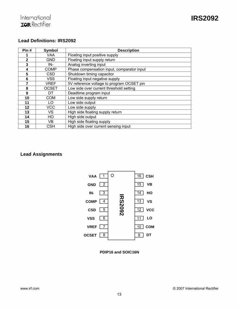
1 VAA Floating input positive supply 2 GND Floating input supply return 3 IN- Analog inverting input 4 COMP Phase compensation input, comparator input 5 CSD Shutdown timing capacitor 6 VSS Floating input negative supply 7 VREF 5V reference voltage to program OCSET pin 8 OCSET Low side over current threshold setting 9 DT Deadtime program input
10 COM Low side supply return 11 LO Low side output 12 VCC Low side supply 13 VS High side floating supply return 14 HO High side output 15 VB High side floating supply 16 CSH High side over current sensing input
The information provided in this document is believed to be accurate and reliable. However, International Rectifier assumes no responsibility for
the consequences of the use of this information. International Rectifier assumes no responsibility for any infringement of patents or of other rights of third parties which may result from the use of this information. No license is granted by implication or otherwise under any patent or patent rights of International Rectifier. The specifications mentioned in this document are subject to change without notice. This document
supersedes and replaces all information previously supplied.
For technical support, please contact IR’s Technical Assistance Center http://www.irf.com/technical-info/
WORLD HEADQUARTERS:
233 Kansas St., El Segundo, California 90245 Tel: (310) 252-7105