To learn more about ON Semiconductor, please visit our website at www.onsemi.com Is Now Part of ON Semiconductor and the ON Semiconductor logo are trademarks of Semiconductor Components Industries, LLC dba ON Semiconductor or its subsidiaries in the United States and/or other countries. ON Semiconductor owns the rights to a number of patents, trademarks, copyrights, trade secrets, and other intellectual property. A listing of ON Semiconductor’s product/patent coverage may be accessed at www.onsemi.com/site/pdf/Patent-Marking.pdf. ON Semiconductor reserves the right to make changes without further notice to any products herein. ON Semiconductor makes no warranty, representation or guarantee regarding the suitability of its products for any particular purpose, nor does ON Semiconductor assume any liability arising out of the application or use of any product or circuit, and specifically disclaims any and all liability, including without limitation special, consequential or incidental damages. Buyer is responsible for its products and applications using ON Semiconductor products, including compliance with all laws, regulations and safety requirements or standards, regardless of any support or applications information provided by ON Semiconductor. “Typical” parameters which may be provided in ON Semiconductor data sheets and/or specifications can and do vary in different applications and actual performance may vary over time. All operating parameters, including “Typicals” must be validated for each customer application by customer’s technical experts. ON Semiconductor does not convey any license under its patent rights nor the rights of others. ON Semiconductor products are not designed, intended, or authorized for use as a critical component in life support systems or any FDA Class 3 medical devices or medical devices with a same or similar classification in a foreign jurisdiction or any devices intended for implantation in the human body. Should Buyer purchase or use ON Semiconductor products for any such unintended or unauthorized application, Buyer shall indemnify and hold ON Semiconductor and its officers, employees, subsidiaries, affiliates, and distributors harmless against all claims, costs, damages, and expenses, and reasonable attorney fees arising out of, directly or indirectly, any claim of personal injury or death associated with such unintended or unauthorized use, even if such claim alleges that ON Semiconductor was negligent regarding the design or manufacture of the part. ON Semiconductor is an Equal Opportunity/Affirmative Action Employer. This literature is subject to all applicable copyright laws and is not for resale in any manner.
Transcript
To learn more about ON Semiconductor, please visit our website at www.onsemi.com
Is Now Part of
ON Semiconductor and the ON Semiconductor logo are trademarks of Semiconductor Components Industries, LLC dba ON Semiconductor or its subsidiaries in the United States and/or other countries. ON Semiconductor owns the rights to a number of patents, trademarks, copyrights, trade secrets, and other intellectual property. A listing of ON Semiconductor’s product/patent coverage may be accessed at www.onsemi.com/site/pdf/Patent-Marking.pdf. ON Semiconductor reserves the right to make changes without further notice to any products herein. ON Semiconductor makes no warranty, representation or guarantee regarding the suitability of its products for any particular purpose, nor does ON Semiconductor assume any liability arising out of the application or use of any product or circuit, and specifically disclaims any and all liability, including without limitation special, consequential or incidental damages. Buyer is responsible for its products and applications using ON Semiconductor products, including compliance with all laws, regulations and safety requirements or standards, regardless of any support or applications information provided by ON Semiconductor. “Typical” parameters which may be provided in ON Semiconductor data sheets and/or specifications can and do vary in different applications and actual performance may vary over time. All operating parameters, including “Typicals” must be validated for each customer application by customer’s technical experts. ON Semiconductor does not convey any license under its patent rights nor the rights of others. ON Semiconductor products are not designed, intended, or authorized for use as a critical component in life support systems or any FDA Class 3 medical devices or medical devices with a same or similar classification in a foreign jurisdiction or any devices intended for implantation in the human body. Should Buyer purchase or use ON Semiconductor products for any such unintended or unauthorized application, Buyer shall indemnify and hold ON Semiconductor and its officers, employees, subsidiaries, affiliates, and distributors harmless against all claims, costs, damages, and expenses, and reasonable attorney fees arising out of, directly or indirectly, any claim of personal injury or death associated with such unintended or unauthorized use, even if such claim alleges that ON Semiconductor was negligent regarding the design or manufacture of the part. ON Semiconductor is an Equal Opportunity/Affirmative Action Employer. This literature is subject to all applicable copyright laws and is not for resale in any manner.
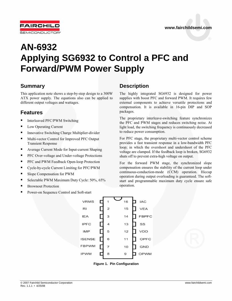
AN-6932 Applying SG6932 to Control a PFC and Forward/PWM Power Supply
Summary This application note shows a step-by-step design to a 300W ATX power supply. The equations also can be applied to different output voltages and wattages.
Features Interleaved PFC/PWM Switching Low Operating Current Innovative Switching Charge Multiplier-divider Multi-vector Control for Improved PFC Output
Transient Response Average Current Mode for Input-current Shaping PFC Over-voltage and Under-voltage Protections PFC and PWM Feedback Open-loop Protection Cycle-by-cycle Current Limiting for PFC/PWM Slope Compensation for PWM Selectable PWM Maximum Duty Cycle: 50%, 65% Brownout Protection Power-on Sequence Control and Soft-start
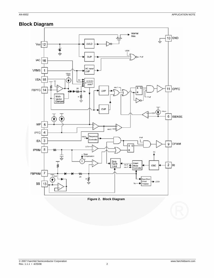
Description The highly integrated SG6932 is designed for power supplies with boost PFC and forward PWM. It requires few external components to achieve versatile protections and compensation. It is available in 16-pin DIP and SOP packages.
The proprietary interleave-switching feature synchronizes the PFC and PWM stages and reduces switching noise. At light load, the switching frequency is continuously decreased to reduce power consumption.
For PFC stage, the proprietary multi-vector control scheme provides a fast transient response in a low-bandwidth PFC loop; in which the overshoot and undershoot of the PFC voltage are clamped. If the feedback loop is broken, SG6932 shuts off to prevent extra-high voltage on output.
For the forward PWM stage, the synchronized slope compensation ensures the stability of the current loop under continuous-conduction-mode (CCM) operation. Hiccup operation during output overloading is guaranteed. The soft-start and programmable maximum duty cycle ensure safe operation.
Power-On Sequence SG6932 is enabled when the line voltage is higher than the brownout threshold. Once the SG6932 is active, the PFC stage is enabled first. Following a 4ms delay after FBPFC voltage exceeds 2.7V, the PWM stage is enabled.
PFC Inductor The switching frequency, output power, efficiency, maximum ripple current, and the minimum input voltage should be defined before determining the inductance the of PFC inductor. The following equations are utilized to determine the inductance of the PFC inductor. The maximum ripple current is set as 20% ~ 30% of maximum input current.
( )
If/D2V
L
dtdiLV
V2V
1D
V3.0/PI
)MIN(IN
O
)MIN(IN
)MIN(INOUT
Δ
••=
=
•−=
•=Δ
η
(1)
For a 300W ATX power supply: η=0.75
VIN(MIN)=90VAC
f=65KHz
VO=400V
ΔI=1.33ª
D=0.68
L=1mH
PFC Capacitor An advantage of using interleaving switching of PFC and PWM stage is to reduce the switching noise and stress to the boost capacitor. The ESR requirement of boost capacitor is relaxed.
Figure 4. Interleaving Switching
The boost capacitor value is chosen to maintain output voltage a hold-up time in the event the line voltage is suddenly removed.
( )( ) 2
)MIN(o2
ripplenormal(o
upholdPWMOUTO
VV)V
t/P2C
−−
•> − η (2)
where Vo(Min) is the minimum output voltage in accordance with the requirement of the specification.
For a 300W ATX power supply, the capacitor is determined as follow:
( ) µF5.1525.246)20400(
ms178.0/W3002C 22O =−−
•> (3)
Because the capacitor includes ±20% variation, the capacitor 180µF is chosen.
Boost Diode and Switch The fast reverse-recovery time of the boost diode is required to reduce the power losses and the EMI. A 500V voltage rating is chosen to withstand 400V boosts potential. The average and peak currents, respectively, through the boost diode and the switch are:
A08.875
7.0/3002I
V/P2I
A15.575
7.0/30022I
V/P22I
PEAK
)Brownout(RMSOUT
PEAK
AVG
)Brownout(RMSOUT
AVG
=•
=
•=
=••
=
•=
η
π
πη
(4)
Oscillation and Green Mode The resistor RI connected from the RI to GND pin programs the switching frequency, given by:
( ) ( )KHzKR
1560
IfPWM Ω
= (5)
For example, a 24kΩ resistor RI results in a 65kHz switching frequency. The range of the switching frequency is recommended between 33kHz ~ 130kHz.
The green-mode function of SG6932 provides off-time modulation to reduce the switching frequency in light-load and no-load conditions. The feedback voltage of FBPWM pin is taken as reference. When the feedback voltage is lower than about 2.1V, the switching frequency decreases accordingly. Most of losses in a switching-mode power supply are proportional to the switching frequency; therefore, the off-time modulation reduces the power consumption of the power supply in light-load and no-load conditions. For a typical case of RI = 24KΩ, the switching frequency is 65kHz at nominal load and decreases to 20kHz at no load.
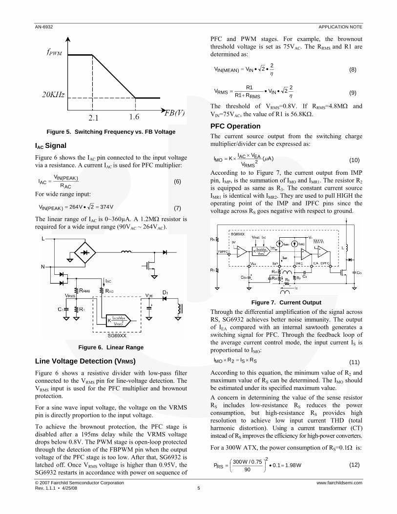
IAC Signal Figure 6 shows the IAC pin connected to the input voltage via a resistance. A current IAC is used for PFC multiplier:
AC
)PEAK(INAC R
VI = (6)
For wide range input:
V3742V264V )PEAK(IN =•= (7)
The linear range of IAC is 0~360µA. A 1.2MΩ resistor is required for a wide input range (90VAC ~ 264VAC).
Figure 6. Linear Range
Line Voltage Detection (VRMS) Figure 6 shows a resistive divider with low-pass filter connected to the VRMS pin for line-voltage detection. The VRMS input is used for the PFC multiplier and brownout protection.
For a sine wave input voltage, the voltage on the VRMS
pin is directly proportion to the input voltage.
To achieve the brownout protection, the PFC stage is disabled after a 195ms delay while the VRMS voltage drops below 0.8V. The PWM stage is open-loop protected through the detection of the FBPWM pin when the output voltage of the PFC stage is too low. After that, SG6932 is latched off. Once VRMS voltage is higher than 0.95V, the SG6932 restarts in accordance with power on sequence of
PFC and PWM stages. For example, the brownout threshold voltage is set as 75VAC. The RRMS and R1 are determined as:
η22VV IN)MEAN(IN ••= (8)
η22V
R1R1RV INRMS
RMS ••+
= (9)
The threshold of VRMS=0.8V. If RRMS=4.8MΩ and VIN=75VAC, the value of R1 is 56.8KΩ.
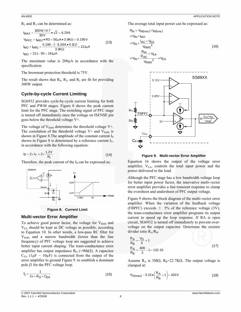
PFC Operation The current source output from the switching charge multiplier/divider can be expressed as:
)A(V
VIKI 2RMS
EAACMO μ×
×= (10)
According to to Figure 7, the current output from IMP pin, IMP, is the summation of IMO and IMR1. The resistor R2 is equipped as same as R3. The constant current source IMR1 is identical with IMR2. They are used to pull HIGH the operating point of the IMP and IPFC pins since the voltage across RS goes negative with respect to ground.
Figure 7. Current Output Through the differential amplification of the signal across RS, SG6932 achieves better noise immunity. The output of IEA compared with an internal sawtooth generates a switching signal for PFC. Through the feedback loop of the average current control mode, the input current IS is proportional to IMO:
SS2MO RIRI ×=× (11)
According to this equation, the minimum value of R2 and maximum value of RS can be determined. The IMO should be estimated under its specified maximum value. A concern in determining the value of the sense resistor RS includes low-resistance RS reduces the power consumption, but high-resistance RS provides high resolution to achieve low input current THD (total harmonic distortion). Using a current transformer (CT) instead of RS improves the efficiency for high-power converters.
For a 300W ATX, the power consumption of RS=0.1Ω is:
The maximum value is 200µA in accordance with the specification.
The brownout protection threshold is 75V.
The result shows that RS, R2, and R3 are fit for providing 300W output.
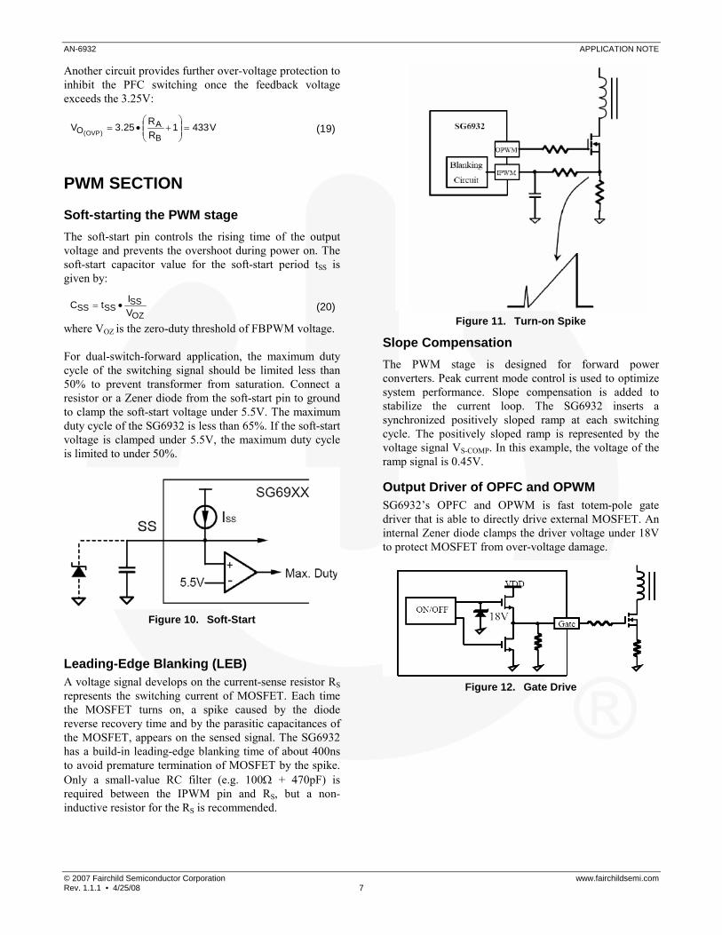
Cycle-by-cycle Current Limiting SG6932 provides cycle-by-cycle current limiting for both PFC and PWM stages. Figure 8 shows the peak current limit for the PFC stage. The switching signal of PFC stage is turned off immediately once the voltage on ISENSE pin goes below the threshold voltage V+.
The voltage of VRMS determines the threshold voltage V+. The correlation of the threshold voltage V+ and VRMS is shown in Figure 8.The amplitude of the constant current IP shown in Figure 8 is determined by a reference current IT, in accordance with the following equation:
IT R
V2.12I2Ip ×=×= (14)
Therefore, the peak current of the IS can be expressed as;
Figure 8. Current Limit
Multi-vector Error Amplifier To achieve good power factor, the voltage for VRMS and VEA should be kept as DC voltage as possible, according to Equation 10. In other words, a low-pass RC filter for VRMS and a narrow bandwidth (lower than the line frequency) of PFC voltage loop are suggested to achieve better input current shaping. The trans-conductance error amplifier has output impedance RO (>90kΩ). A capacitor CEA (1µF ~ 10µF) is connected from the output of the error amplifier to ground Figure 9. to establish a dominant pole f1 for the PFC voltage loop.
EAO1 CR2
1f××
=π
(15)
The average total input power can be expressed as:
( ) ( )
EA2RMS
EAACIN
IN
2RMS
EAACIN
MOIN
rmsINrmsININ
VV
VRR
V
V
VIV
IV
IVP
∞×
×∞
××∞
×∞
×=
(16)
Figure 9. Multi-vector Error Amplifier
Equation 16 shows the output of the voltage error amplifier, VEA, controls the total input power and the power delivered to the load.
Although the PFC stage has a low bandwidth voltage loop for better input power factor, the innovative multi-vector error amplifier provides a fast transient response to clamp the overshoot and undershoot of PFC output voltage.
Figure 9 shows the block diagram of the multi-vector error amplifier. When the variation of the feedback voltage (FBPFC) exceeds ± 5% of the reference voltage (3V), the trans-conductance error amplifier programs its output current to speed up the loop response. If RA is open circuit, SG6932 is turned off immediately to prevent over-voltage on the output capacitor. Determine the resistor divider ratio RA/RB:
33.13213
400RR
13
VRR
BA
OBA
=−=
== (17)
Assume RA is 3MΩ, RB=22.7KΩ. The output voltage is clamped at:
Another circuit provides further over-voltage protection to inhibit the PFC switching once the feedback voltage exceeds the 3.25V:
V4331RR25.3V
BA
O )OVP(=⎟⎟
⎠
⎞⎜⎜⎝
⎛+•= (19)
PWM SECTION
Soft-starting the PWM stage The soft-start pin controls the rising time of the output voltage and prevents the overshoot during power on. The soft-start capacitor value for the soft-start period tSS is given by:
OZSS
SSSS VItC •= (20)
where VOZ is the zero-duty threshold of FBPWM voltage. For dual-switch-forward application, the maximum duty cycle of the switching signal should be limited less than 50% to prevent transformer from saturation. Connect a resistor or a Zener diode from the soft-start pin to ground to clamp the soft-start voltage under 5.5V. The maximum duty cycle of the SG6932 is less than 65%. If the soft-start voltage is clamped under 5.5V, the maximum duty cycle is limited to under 50%.
Figure 10. Soft-Start
Leading-Edge Blanking (LEB) A voltage signal develops on the current-sense resistor RS represents the switching current of MOSFET. Each time the MOSFET turns on, a spike caused by the diode reverse recovery time and by the parasitic capacitances of the MOSFET, appears on the sensed signal. The SG6932 has a build-in leading-edge blanking time of about 400ns to avoid premature termination of MOSFET by the spike. Only a small-value RC filter (e.g. 100Ω + 470pF) is required between the IPWM pin and RS, but a non-inductive resistor for the RS is recommended.
Figure 11. Turn-on Spike
Slope Compensation The PWM stage is designed for forward power converters. Peak current mode control is used to optimize system performance. Slope compensation is added to stabilize the current loop. The SG6932 inserts a synchronized positively sloped ramp at each switching cycle. The positively sloped ramp is represented by the voltage signal VS-COMP. In this example, the voltage of the ramp signal is 0.45V.
Output Driver of OPFC and OPWM SG6932’s OPFC and OPWM is fast totem-pole gate driver that is able to directly drive external MOSFET. An internal Zener diode clamps the driver voltage under 18V to protect MOSFET from over-voltage damage.
Over-Current Protection (OCP) and Short-Circuit Protection (SCP) SG6932’s OCP and SCP is based on the detection of feedback signal on FBPWM pin. As shown in Figure 13;
if over current or short circuit occurrs, FBPWM is pulled to a high voltage through the feedback loop. After a 95ms debounce time, SG6932 is turned off. The 600ms time-out signal prevents SG6932 from being latched off when the input voltage is fast on/off.
Figure 13. Constant Power Limit Compensation
Forward Transformer The topology used in this application note is dual switch forward, so the maximum duty cycle must be limited less than 50%. For transient load, efficiency, and hold-up time consideration, 30% duty cycle is chosen for determining the turn ratio of the transformer.
The secondary voltage of 12V, 5V should be:
( )
( ) FDS5
V5SEC
12FD12
V12SEC
VDVV
Or
VD
VV
+=
+=
(21)
where: VFD12 and VFD5 are the forward voltage of rectifier diodes of 12V and 5V outputs; D is duty cycle of switching signal for steady state operation.
Assume VFD12 and VFD5 are 0.5V, D is 30% duty cycle, VSEC(12V) is 40.5V, and VSEC(5V) is 17.17V.
The turn ratio is as below:
)V5(SECO
)V5(SEC
)V(PRI
)V12(SECO
)V12(SEC
)V(PRI
VV
NN
Or
VV
NN
O
O
=
=
(22)
If VO is 400V, the turn ratio is 69:7:3.
The primary winding turns is calculated by Faraday’s Law:
6910cm07.1G2500Khz65/3.0V400N
f/DAeBN
tAeBN
V
82)V(PRI
MAX)V(PRIMAX)V(PRIO
O
OO
=••
•=
•Δ•=
Δ
•Δ•=
(23)
Choose ERL35 and the turns in 69:7:3. If the topology is a single switch forward, the maximum duty cycle can be designed around 40%~45% for the steady-state operation. The turns of the transformer can be calculated by above equations.
Lab Note Before rework or solder/de-solder on the power supply, discharge primary capacitors by an external bleeding resistor. Otherwise, high voltage might destroy the PWM IC during solder/de-solder operation.
This device is sensitive to ESD discharge. To improve production yield, the production line should be ESD protected according to ANSI ESD S1.1, ESD S1.4, ESD S7.1, ESD STM 12.1, and EOS/ESD S6.1.
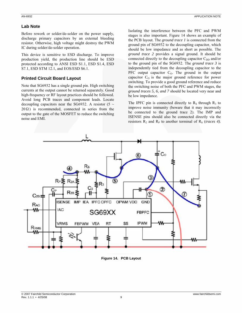
Printed Circuit Board Layout Note that SG6932 has a single ground pin. High switching currents at the output cannot be returned separately. Good high-frequency or RF layout practices should be followed. Avoid long PCB traces and component leads. Locate decoupling capacitors near the SG6932. A resistor (5 ~ 20Ω) is recommended, connected in series from the output to the gate of the MOSFET to reduce the switching noise and EMI.
Isolating the interference between the PFC and PWM stages is also important. Figure 14 shows an example of the PCB layout. The ground trace 1 is connected from the ground pin of SG6932 to the decoupling capacitor, which should be low impedance and as short as possible. The ground trace 2 provides a signal ground. It should be connected directly to the decoupling capacitor CDD and/or to the ground pin of the SG6932. The ground trace 3 is independently tied from the decoupling capacitor to the PFC output capacitor CO. The ground in the output capacitor CO is the major ground reference for power switching. To provide a good ground reference and reduce the switching noise of both the PFC and PWM stages, the ground traces 5, 6, and 7 should be located very near and be low impedance.
The IPFC pin is connected directly to RS through R3 to improve noise immunity (beware that it may incorrectly be connected to the ground trace 2). The IMP and ISENSE pins should also be connected directly via the resistors R2 and RP to another terminal of RS (traces 4).
Related Datasheets SG6932 — PFC / Forward PWM Controller
DISCLAIMER FAIRCHILD SEMICONDUCTOR RESERVES THE RIGHT TO MAKE CHANGES WITHOUT FURTHER NOTICE TO ANY PRODUCTS HEREIN TO IMPROVE RELIABILITY, FUNCTION, OR DESIGN. FAIRCHILD DOES NOT ASSUME ANY LIABILITY ARISING OUT OF THE APPLICATION OR USE OF ANY PRODUCT OR CIRCUIT DESCRIBED HEREIN; NEITHER DOES IT CONVEY ANY LICENSE UNDER ITS PATENT RIGHTS, NOR THE RIGHTS OF OTHERS. LIFE SUPPORT POLICY FAIRCHILD’S PRODUCTS ARE NOT AUTHORIZED FOR USE AS CRITICAL COMPONENTS IN LIFE SUPPORT DEVICES OR SYSTEMS WITHOUT THE EXPRESS WRITTEN APPROVAL OF THE PRESIDENT OF FAIRCHILD SEMICONDUCTOR CORPORATION. As used herein: 1. Life support devices or systems are devices or systems
which, (a) are intended for surgical implant into the body, or (b) support or sustain life, or (c) whose failure to perform when properly used in accordance with instructions for use provided in the labeling, can be reasonably expected to result in significant injury to the user.
2. A critical component is any component of a life support device or system whose failure to perform can be reasonably expected to cause the failure of the life support device or system, or to affect its safety or effectiveness.
www.onsemi.com1
ON Semiconductor and are trademarks of Semiconductor Components Industries, LLC dba ON Semiconductor or its subsidiaries in the United States and/or other countries.ON Semiconductor owns the rights to a number of patents, trademarks, copyrights, trade secrets, and other intellectual property. A listing of ON Semiconductor’s product/patentcoverage may be accessed at www.onsemi.com/site/pdf/Patent−Marking.pdf. ON Semiconductor reserves the right to make changes without further notice to any products herein.ON Semiconductor makes no warranty, representation or guarantee regarding the suitability of its products for any particular purpose, nor does ON Semiconductor assume any liabilityarising out of the application or use of any product or circuit, and specifically disclaims any and all liability, including without limitation special, consequential or incidental damages.Buyer is responsible for its products and applications using ON Semiconductor products, including compliance with all laws, regulations and safety requirements or standards,regardless of any support or applications information provided by ON Semiconductor. “Typical” parameters which may be provided in ON Semiconductor data sheets and/orspecifications can and do vary in different applications and actual performance may vary over time. All operating parameters, including “Typicals” must be validated for each customerapplication by customer’s technical experts. ON Semiconductor does not convey any license under its patent rights nor the rights of others. ON Semiconductor products are notdesigned, intended, or authorized for use as a critical component in life support systems or any FDA Class 3 medical devices or medical devices with a same or similar classificationin a foreign jurisdiction or any devices intended for implantation in the human body. Should Buyer purchase or use ON Semiconductor products for any such unintended or unauthorizedapplication, Buyer shall indemnify and hold ON Semiconductor and its officers, employees, subsidiaries, affiliates, and distributors harmless against all claims, costs, damages, andexpenses, and reasonable attorney fees arising out of, directly or indirectly, any claim of personal injury or death associated with such unintended or unauthorized use, even if suchclaim alleges that ON Semiconductor was negligent regarding the design or manufacture of the part. ON Semiconductor is an Equal Opportunity/Affirmative Action Employer. Thisliterature is subject to all applicable copyright laws and is not for resale in any manner.
PUBLICATION ORDERING INFORMATIONN. American Technical Support: 800−282−9855 Toll FreeUSA/Canada
Europe, Middle East and Africa Technical Support:Phone: 421 33 790 2910
Japan Customer Focus CenterPhone: 81−3−5817−1050
www.onsemi.com
LITERATURE FULFILLMENT:Literature Distribution Center for ON Semiconductor19521 E. 32nd Pkwy, Aurora, Colorado 80011 USAPhone: 303−675−2175 or 800−344−3860 Toll Free USA/CanadaFax: 303−675−2176 or 800−344−3867 Toll Free USA/CanadaEmail: [email protected]
ON Semiconductor Website: www.onsemi.com
Order Literature: http://www.onsemi.com/orderlit
For additional information, please contact your localSales Representative