+ All Categories
Home > Documents > IS42S16400F IS45S16400F - ISSI IS42S16400F IS45S16400F GENERAL DESCRIPTION The 64Mb SDRAM is a high...

IS42S16400F IS45S16400F - ISSI IS42S16400F IS45S16400F GENERAL DESCRIPTION The 64Mb SDRAM is a high...

Date post: 22-Mar-2018
Category:
Upload: vuminh
View: 215 times
Download: 0 times
Share this document with a friend
59
Integrated Silicon Solution, Inc. — www.issi.com 1 Rev. I 12/01/2011 Copyright © 2011 Integrated Silicon Solution, Inc. All rights reserved. ISSI reserves the right to make changes to this specification and its products at any time without notice. ISSI assumes no liability arising out of the application or use of any information, products or services described herein. Customers are advised to obtain the latest version of this device specification before relying on any published information and before placing orders for products. Integrated Silicon Solution, Inc. does not recommend the use of any of its products in life support applications where the failure or malfunction of the product can reasonably be ex- pected to cause failure of the life support system or to significantly affect its safety or effectiveness.Products are not authorized for use in such applications unless Integrated Silicon Solution, Inc. receives written assurance to its satisfaction, that: a.) the risk of injury or damage has been minimized; b.) the user assume all such risks; and c.) potential liability of Integrated Silicon Solution, Inc is adequately protected under the circumstances IS42S16400F IS45S16400F FEATURES Clock frequency: 200, 166, 143, 133 MHz Fully synchronous; all signals referenced to a positive clock edge Internal bank for hiding row access/precharge Single 3.3V power supply LVTTL interface Programmable burst length – (1, 2, 4, 8, full page) Programmable burst sequence: Sequential/Interleave Self refresh modes Auto refresh (CBR) 4096 refresh cycles every 64 ms (Com, Ind, A1 grade) or 16ms (A2 grade) Random column address every clock cycle Programmable CAS latency (2, 3 clocks) Burst read/write and burst read/single write operations capability Burst termination by burst stop and precharge command OPTIONS Package: 54-pin TSOP II 54-ball FBGA (8mm x 8mm) Operating Temperature Range Commercial (0 o C to +70 o C) Industrial (-40 o C to +85 o C) Automotive Grade A1 (-40 o C to +85 o C) Automotive Grade A2 (-40 o C to +105 o C) OVERVIEW ISSI's 64Mb Synchronous DRAM is organized as 1,048,576 bits x 16-bit x 4-bank for improved performance. The synchronous DRAMs achieve high-speed data transfer using pipeline architecture. All inputs and outputs signals refer to the rising edge of the clock input. 1 Meg Bits x 16 Bits x 4 Banks (64-MBIT) SYNCHRONOUS DYNAMIC RAM DECEMBER 2011 KEY TIMING PARAMETERS Parameter -5 -6 -7 Unit Clk Cycle Time CAS Latency = 3 5 6 7 ns CAS Latency = 2 7.5 7.5 7.5 ns Clk Frequency CAS Latency = 3 200 166 143 Mhz CAS Latency = 2 133 133 133 Mhz Access Time from Clock CAS Latency = 3 5 5.4 5.4 ns CAS Latency = 2 6 6 6 ns Parameter 4M x 16 Configuration 1M x 16 x 4 banks Refresh Count Com./Ind. A1 A2 4K/64ms 4K/64ms 4K/16ms Row Addresses A0-A11 Column Addresses A0-A7 Bank Address Pins BA0, BA1 Auto Precharge Pins A10/AP ADDRESS TABLE
Transcript

Integrated Silicon Solution, Inc. — www.issi.com 1Rev. I12/01/2011

Copyright©2011IntegratedSiliconSolution,Inc.Allrightsreserved.ISSIreservestherighttomakechangestothisspecificationanditsproductsatanytimewithoutnotice.ISSIassumesnoliabilityarisingoutoftheapplicationoruseofanyinformation,productsorservicesdescribedherein.Customersareadvisedtoobtainthelatestversionofthisdevicespecificationbeforerelyingonanypublishedinformationandbeforeplacingordersforproducts.

IntegratedSiliconSolution,Inc.doesnotrecommendtheuseofanyofitsproductsinlifesupportapplicationswherethefailureormalfunctionoftheproductcanreasonablybeex-pectedtocausefailureofthelifesupportsystemortosignificantlyaffectitssafetyoreffectiveness.ProductsarenotauthorizedforuseinsuchapplicationsunlessIntegratedSiliconSolution,Inc.receiveswrittenassurancetoitssatisfaction,that:a.)theriskofinjuryordamagehasbeenminimized;b.)theuserassumeallsuchrisks;andc.)potentialliabilityofIntegratedSiliconSolution,Incisadequatelyprotectedunderthecircumstances

IS42S16400FIS45S16400F

FEATURES• Clockfrequency:200,166,143,133MHz

• Fullysynchronous;allsignalsreferencedtoapositiveclockedge

• Internalbankforhidingrowaccess/precharge

• Single3.3Vpowersupply

• LVTTLinterface

• Programmableburstlength–(1,2,4,8,fullpage)

• Programmableburstsequence:Sequential/Interleave

• Selfrefreshmodes

• Autorefresh(CBR)

• 4096refreshcyclesevery64ms(Com,Ind,A1grade)or16ms(A2grade)

• Randomcolumnaddresseveryclockcycle

• ProgrammableCASlatency(2,3clocks)

• Burstread/writeandburstread/singlewriteoperationscapability

• Burstterminationbyburststopandprechargecommand

OPTIONS• Package:

54-pinTSOPII54-ballFBGA(8mmx8mm)

• OperatingTemperatureRangeCommercial(0oCto+70oC)Industrial(-40oCto+85oC)AutomotiveGradeA1(-40oCto+85oC)AutomotiveGradeA2(-40oCto+105oC)

OVERVIEWISSI's64MbSynchronousDRAMisorganizedas1,048,576bits x 16-bit x 4-bank for improved performance. Thesynchronous DRAMs achieve high-speed data transferusingpipelinearchitecture.Allinputsandoutputssignalsrefertotherisingedgeoftheclockinput.

1 Meg Bits x 16 Bits x 4 Banks (64-MBIT) SYNCHRONOUS DYNAMIC RAM

DECEMBER 2011

KEY TIMING PARAMETERS

Parameter -5 -6 -7 Unit

ClkCycleTime CASLatency=3 5 6 7 ns CASLatency=2 7.5 7.5 7.5 ns

ClkFrequency CASLatency=3 200 166 143 Mhz CASLatency=2 133 133 133 Mhz

AccessTimefromClock CASLatency=3 5 5.4 5.4 ns CASLatency=2 6 6 6 ns

Parameter 4M x 16Configuration 1M x 16 x 4

banksRefresh Count

Com./Ind.A1A2

4K/64ms4K/64ms4K/16ms

Row Addresses A0-A11Column Addresses A0-A7Bank Address Pins BA0, BA1Auto Precharge Pins A10/AP

ADDRESS TABLE

2 Integrated Silicon Solution, Inc. — www.issi.com Rev. I

12/01/2011

IS42S16400FIS45S16400F

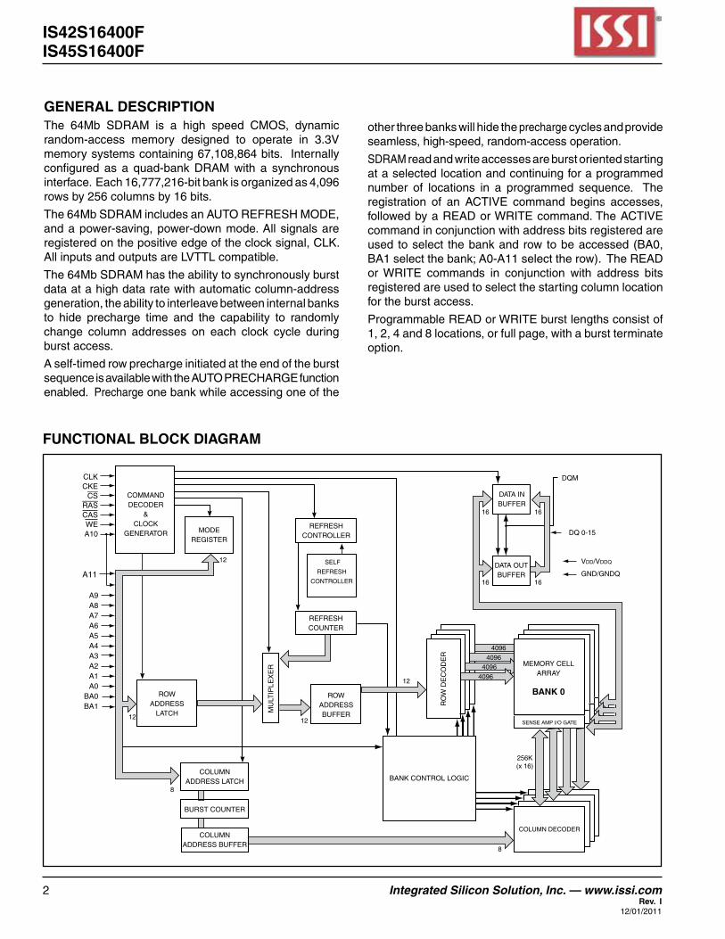
GENERAL DESCRIPTIONThe 64Mb SDRAM is a high speed CMOS, dynamicrandom-access memory designed to operate in 3.3Vmemorysystemscontaining67,108,864bits. Internallyconfigured as a quad-bank DRAM with a synchronousinterface.Each16,777,216-bitbankisorganizedas4,096rowsby256columnsby16bits.

The64MbSDRAMincludesanAUTOREFRESHMODE,andapower-saving,power-downmode.Allsignalsareregisteredonthepositiveedgeoftheclocksignal,CLK.AllinputsandoutputsareLVTTLcompatible.

The64MbSDRAMhastheabilitytosynchronouslyburstdataatahighdataratewithautomaticcolumn-addressgeneration,theabilitytointerleavebetweeninternalbanksto hide precharge time and the capability to randomlychange column addresses on each clock cycle duringburstaccess.

Aself-timedrowprechargeinitiatedattheendoftheburstsequenceisavailablewiththeAUTOPRECHARGEfunctionenabled. Prechargeonebankwhileaccessingoneofthe

otherthreebankswillhidetheprechargecyclesandprovideseamless,high-speed,random-accessoperation.

SDRAMreadandwriteaccessesareburstorientedstartingataselectedlocationandcontinuingforaprogrammednumber of locations in a programmed sequence. Theregistration of an ACTIVE command begins accesses,followedbyaREADorWRITEcommand.TheACTIVEcommandinconjunctionwithaddressbitsregisteredareusedtoselect thebankandrowtobeaccessed(BA0,BA1selectthebank;A0-A11selecttherow).TheREADor WRITE commands in conjunction with address bitsregisteredareusedtoselectthestartingcolumnlocationfortheburstaccess.

ProgrammableREADorWRITEburstlengthsconsistof1,2,4and8locations,orfullpage,withaburstterminateoption.

CLKCKECSRASCASWEA10

A9A8A7A6A5A4A3A2A1A0

BA0BA1

A11

COMMANDDECODER

&CLOCK

GENERATOR MODEREGISTER

REFRESHCONTROLLER

REFRESHCOUNTER

SELF

REFRESH

CONTROLLER

ROWADDRESS

LATCH MU

LTIP

LEX

ER

COLUMNADDRESS LATCH

BURST COUNTER

COLUMNADDRESS BUFFER

COLUMN DECODER

DATA INBUFFER

DATA OUTBUFFER

DQM

DQ 0-15

VDD/VDDQ

GND/GNDQ

12

12

8

12

12

8

16

16 16

16

256K(x 16)

4096

4096

4096

RO

W D

EC

OD

ER 4096

MEMORY CELLARRAY

BANK 0

SENSE AMP I/O GATE

BANK CONTROL LOGIC

ROWADDRESSBUFFER

FUNCTIONAL BLOCK DIAGRAM

Integrated Silicon Solution, Inc. — www.issi.com 3Rev. I12/01/2011

IS42S16400FIS45S16400F

PIN CONFIGURATIONPACKAge Code: B 54 BALL fBgA (Top View) (8 mm x 8 mm Body, 0.8 mm Ball Pitch)

1 2 3 4 5 6 7 8 9

A

B

C

D

E

F

G

H

J

DQ15

DQ13

DQ11

DQ9

NC

CLK

A11

A7

A5

GNDQ

VDDQ

GNDQ

VDDQ

GND

CKE

A9

A6

A4

VDDQ

GNDQ

VDDQ

GNDQ

VDD

CAS

BA0

A0

A3

DQ0

DQ2

DQ4

DQ6

DQML

RAS

BA1

A1

A2

GND

DQ14

DQ12

DQ10

DQ8

DQMH

NC

A8

GND

VDD

DQ1

DQ3

DQ5

DQ7

WE

CS

A10

VDD

PIN DESCRIPTIONSA0-A11 Row Address InputA0-A7 Column Address InputBA0, BA1 Bank Select AddressesdQ0 to dQ15 data I/oCLK System Clock InputCKe Clock enableCS Chip SelectRAS Row Address Strobe CommandCAS Column Address Strobe Command

WE Write enableLdQM, UdQM x16 Input/output MaskVdd PowergNd groundVddq Power Supply for I/o PingNdQ ground for I/o PinNC No Connection

4 Integrated Silicon Solution, Inc. — www.issi.com Rev. I

12/01/2011

IS42S16400FIS45S16400F

PIN CONFIGURATIONS54 pin TSOP - Type II

PIN DESCRIPTIONSA0-A11 RowAddressInput

A0-A7 ColumnAddressInput

BA0,BA1 BankSelectAddress

DQ0toDQ15 DataI/O

CLK SystemClockInput

CKE ClockEnable

CS ChipSelect

RAS RowAddressStrobeCommand

CAS ColumnAddressStrobeCommand

VDD

DQ0

VDDQ

DQ1

DQ2

GNDQ

DQ3

DQ4

VDDQ

DQ5

DQ6

GNDQ

DQ7

VDD

LDQM

WE

CAS

RAS

CS

BA0

BA1

A10

A0

A1

A2

A3

VDD

1

2

3

4

5

6

7

8

9

10

11

12

13

14

15

16

17

18

19

20

21

22

23

24

25

26

27

54

53

52

51

50

49

48

47

46

45

44

43

42

41

40

39

38

37

36

35

34

33

32

31

30

29

28

GND

DQ15

GNDQ

DQ14

DQ13

VDDQ

DQ12

DQ11

GNDQ

DQ10

DQ9

VDDQ

DQ8

GND

NC

UDQM

CLK

CKE

NC

A11

A9

A8

A7

A6

A5

A4

GND

WE WriteEnable

LDQM x16LowerByte,Input/OutputMask

UDQM x16UpperByte,Input/OutputMask

Vdd Power

GND Ground

Vddq PowerSupplyforI/OPin

GNDq GroundforI/OPin

NC NoConnection

Integrated Silicon Solution, Inc. — www.issi.com 5Rev. I12/01/2011

IS42S16400FIS45S16400F

PIN FUNCTIONS Symbol TSOP Pin No. Type Function (In Detail)

A0-A11 23to26 InputPin AddressInputs:A0-A11aresampledduringtheACTIVE

29to34 command(row-addressA0-A11)andREAD/WRITEcommand(A0-A7

22,35 withA10definingautoprecharge)toselectonelocationoutofthememoryarrayintherespectivebank.A10issampledduringaPRECHARGEcommandtodeter-mineifallbanksaretobeprecharged(A10HIGH)orbankselectedbyBA0,BA1(LOW).Theaddressinputsalsoprovidetheop-codeduringaLOADMODEREGISTERcommand.

BA0,BA1 20,21 InputPin BankSelectAddress:BA0andBA1defineswhichbanktheACTIVE,READ,WRITEorPRECHARGEcommandisbeingapplied.

CAS 17 InputPin CAS,inconjunctionwiththeRASandWE,formsthedevicecommand.Seethe"CommandTruthTable"fordetailsondevicecommands.

CKE 37 InputPin TheCKEinputdetermineswhethertheCLKinputisenabled.ThenextrisingedgeoftheCLKsignalwillbevalidwhenisCKEHIGHandinvalidwhenLOW.WhenCKEisLOW,thedevicewillbeineitherpower-downmode,clocksuspendmode,orselfrefreshmode.CKEisanasynchronousinput.

CLK 38 InputPin CLKisthemasterclockinputforthisdevice.ExceptforCKE,allinputstothisdeviceareacquiredinsynchronizationwiththerisingedgeofthispin.

CS 19 InputPin TheCSinputdetermineswhethercommandinputisenabledwithinthedevice.CommandinputisenabledwhenCSisLOW,anddisabledwithCSisHIGH.ThedeviceremainsinthepreviousstatewhenCSisHIGH.

DQ0to 2,4,5,7,8,10, DQPin DQ0toDQ15areI/Opins.I/Othroughthesepinscanbecontrolledinbyteunits

DQ15 11,13,42,44,45, usingtheLDQMandUDQMpins.

47,48,50,51,53

LDQM, 15,39 InputPin LDQMandUDQMcontrolthelowerandupperbytesoftheI/Obuffers.Inread

UDQM mode,LDQMandUDQMcontroltheoutputbuffer.WhenLDQMorUDQMisLOW,thecorrespondingbufferbyteisenabled,andwhenHIGH,disabled.TheoutputsgototheHIGHimpedancestatewhenLDQM/UDQMisHIGH.Thisfunctioncor-respondstoOEinconventionalDRAMs.Inwritemode,LDQMandUDQMcontroltheinputbuffer.WhenLDQMorUDQMisLOW,thecorrespondingbufferbyteisen-abled,anddatacanbewrittentothedevice.WhenLDQMorUDQMisHIGH,inputdataismaskedandcannotbewrittentothedevice.

RAS 18 InputPin RAS,inconjunctionwithCASandWE,formsthedevicecommand.Seethe"Com-mandTruthTable"itemfordetailsondevicecommands.

WE 16 InputPin WE,inconjunctionwithRASandCAS,formsthedevicecommand.Seethe"Com-mandTruthTable"itemfordetailsondevicecommands.

Vddq 3,9,43,49 PowerSupplyPin Vddqistheoutputbufferpowersupply.

Vdd 1,14,27 PowerSupplyPin Vddisthedeviceinternalpowersupply.

GNdq 6,12,46,52 PowerSupplyPin GNdqistheoutputbufferground.

GNd 28,41,54 PowerSupplyPin GNdisthedeviceinternalground.

6 Integrated Silicon Solution, Inc. — www.issi.com Rev. I

12/01/2011

IS42S16400FIS45S16400F

READTheREADcommandselectsthebankfromBA0,BA1inputsandstartsaburstreadaccesstoanactiverow.InputsA0-A7providesthestartingcolumnlocation.WhenA10isHIGH,thiscommandfunctionsasanAUTOPRECHARGEcommand.Whentheautoprechargeisselected,therowbeingaccessedwillbeprechargedattheendoftheREADburst.TherowwillremainopenforsubsequentaccesseswhenAUTOPRECHARGE isnot selected. DQ’s readdataissubjecttothelogiclevelontheDQMinputstwoclocksearlier.WhenagivenDQMsignalwasregisteredHIGH,thecorrespondingDQ’swillbeHigh-Ztwoclockslater.DQ’swillprovidevaliddatawhentheDQMsignalwasregisteredLOW.

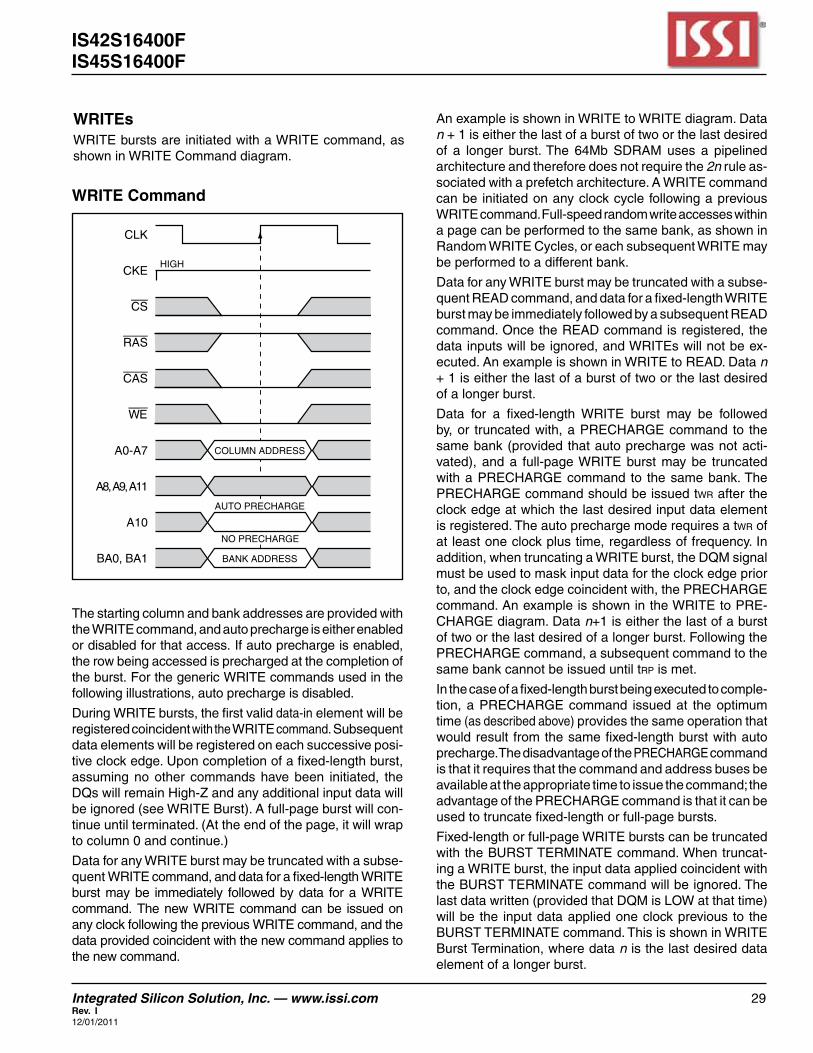
WRITEAburstwriteaccesstoanactiverowisinitiatedwiththeWRITE command. BA0, BA1 inputs selects the bank,and the starting column location is provided by inputsA0-A7.Whether or notAUTO-PRECHARGE is used isdeterminedbyA10.

TherowbeingaccessedwillbeprechargedattheendoftheWRITEburst, ifAUTOPRECHARGE isselected. IfAUTOPRECHARGEisnotselected,therowwillremainopenforsubsequentaccesses.

AmemoryarrayiswrittenwithcorrespondinginputdataonDQ’sandDQMinputlogiclevelappearingatthesametime.DatawillbewrittentomemorywhenDQMsignalisLOW.WhenDQMisHIGH,thecorrespondingdatainputswillbeignored,andaWRITEwillnotbeexecutedtothatbyte/columnlocation.

PRECHARGEThePRECHARGEcommand isused todeactivate theopenrowinaparticularbankortheopenrowinallbanks.BA0,BA1canbeusedtoselectwhichbankisprechargedor they are treated as “Don’t Care”. A10 determineswhetheroneorallbanksareprecharged.Afterexecut-ing this command, the next command for the selectedbank(s)isexecutedafterpassageoftheperiodtRP,whichistheperiodrequiredforbankprecharging.Onceabankhasbeenprecharged,itisintheidlestateandmustbeactivatedpriortoanyREADorWRITEcommandsbeingissuedtothatbank.

AUTO PRECHARGEThe AUTO PRECHARGE function ensures that theprechargeisinitiatedattheearliestvalidstagewithinaburst.Thisfunctionallowsforindividual-bankprechargewithoutrequiringanexplicitcommand.A10canbeusedtoenabletheAUTOPRECHARGEfunction inconjunc-tionwithaspecificREADorWRITEcommand.ForeachindividualREADorWRITEcommand,autoprechargeis

eitherenabledordisabled.AUTOPRECHARGEdoesnotapplyexceptinfull-pageburstmode.UponcompletionoftheREADorWRITEburst,aprechargeofthebank/rowthatisaddressedisautomaticallyperformed.

AUTO REFRESH COMMANDThiscommandexecutestheAUTOREFRESHoperation.Therowaddressandbanktoberefreshedareautomaticallygeneratedduringthisoperation. Thestipulatedperiod(trc)isrequiredforasinglerefreshoperation,andnoothercom-mandscanbeexecutedduringthisperiod. Thiscommandisexecutedatleast4096timeseveryTref.DuringanAUTOREFRESHcommand,addressbitsare“Don’tCare”.ThiscommandcorrespondstoCBRAuto-refresh.

SELF REFRESHDuringtheSELFREFRESHoperation,therowaddresstoberefreshed,thebank,andtherefreshintervalaregen-eratedautomaticallyinternally.SELFREFRESHcanbeusedtoretaindataintheSDRAMwithoutexternalclocking,eveniftherestofthesystemispowereddown.TheSELFREFRESHoperationisstartedbydroppingtheCKEpinfromHIGHtoLOW.DuringtheSELFREFRESHoperationallotherinputstotheSDRAMbecome“Don’tCare”.Thedevicemustremaininselfrefreshmodeforaminimumperiodequaltotrasormayremaininselfrefreshmodeforanindefiniteperiodbeyondthat.TheSELF-REFRESHoperationcontinuesaslongastheCKEpinremainsLOWandthereisnoneedforexternalcontrolofanyotherpins.Thenextcommandcannotbeexecuteduntilthedeviceinternal recovery period (trc) has elapsed. Once CKEgoesHIGH,theNOPcommandmustbeissued(minimumof two clocks) to provide time for the completion of anyinternalrefreshinprogress.Aftertheself-refresh,sinceitisimpossibletodeterminetheaddressofthelastrowtoberefreshed,anAUTO-REFRESHshouldimmediatelybeperformedforalladdresses.

BURST TERMINATETheBURSTTERMINATEcommand forcibly terminatestheburstreadandwriteoperationsbytruncatingeitherfixed-length or full-page bursts and the most recentlyregisteredREADorWRITEcommandpriortotheBURSTTERMINATE.

COMMAND INHIBITCOMMANDINHIBITpreventsnewcommandsfrombeingexecuted.Operationsinprogressarenotaffected,apartfromwhethertheCLKsignalisenabled

NO OPERATION WhenCSislow,theNOPcommandpreventsunwantedcommands from being registered during idle or waitstates.

Integrated Silicon Solution, Inc. — www.issi.com 7Rev. I12/01/2011

IS42S16400FIS45S16400F

LOAD MODE REGISTERDuringtheLOADMODEREGISTERcommandthemoderegisterisloadedfromA0-A11.Thiscommandcanonlybeissuedwhenallbanksareidle.

ACTIVE COMMANDWhen the ACTIVE COMMAND is activated, BA0, BA1inputsselectsabanktobeaccessed,andtheaddressinputsonA0-A11selectstherow.UntilaPRECHARGEcommand is issued to thebank, therowremainsopenforaccesses.

8 Integrated Silicon Solution, Inc. — www.issi.com Rev. I

12/01/2011

IS42S16400FIS45S16400F

TRUTH TABLE – COMMANDS AND DQM OPERATION(1)

FUNCTION CS RAS CAS WE DQM ADDR DQs

COMMANDINHIBIT(NOP) H X X X X X X

NOOPERATION(NOP) L H H H X X X

ACTIVE(Selectbankandactivaterow)(3) L L H H X Bank/Row X

READ(Selectbank/column,startREADburst)(4) L H L H L/H(8) Bank/Col X

WRITE(Selectbank/column,startWRITEburst)(4) L H L L L/H(8) Bank/Col Valid

BURSTTERMINATE L H H L X X Active

PRECHARGE(Deactivaterowinbankorbanks)(5) L L H L X Code X

AUTOREFRESHorSELFREFRESH(6,7) L L L H X X X(Enterselfrefreshmode)

LOADMODEREGISTER(2) L L L L X Op-Code X

WriteEnable/OutputEnable(8) — — — — L — Active

WriteInhibit/OutputHigh-Z(8) — — — — H — High-ZNOTES:1. CKEisHIGHforallcommandsexceptSELFREFRESH.2. A0-A11definetheop-codewrittentothemoderegister.3. A0-A11providerowaddress,andBA0,BA1determinewhichbankismadeactive.4. A0-A7(x16)providecolumnaddress;A10HIGHenablestheautoprechargefeature(nonpersistent),whileA10LOWdisables

autoprecharge;BA0,BA1determinewhichbankisbeingreadfromorwrittento.5. A10LOW:BA0,BA1determinethebankbeingprecharged.A10HIGH:AllbanksprechargedandBA0,BA1are“Don’tCare.”6. AUTOREFRESHifCKEisHIGH,SELFREFRESHifCKEisLOW.7. Internalrefreshcountercontrolsrowaddressing;allinputsandI/Osare“Don’tCare”exceptforCKE.8. ActivatesordeactivatestheDQsduringWRITEs(zero-clockdelay)andREADs(two-clockdelay).

Integrated Silicon Solution, Inc. — www.issi.com 9Rev. I12/01/2011

IS42S16400FIS45S16400F

TRUTH TABLE – CURRENT STATE BANK n, COMMAND TO BANK n (1-6)

CURRENTSTATE COMMAND(ACTION) CS RAS CAS WE

Any COMMANDINHIBIT(NOP/Continuepreviousoperation) H X X X

NOOPERATION(NOP/Continuepreviousoperation) L H H H

Idle ACTIVE(Selectandactivaterow) L L H H

AUTOREFRESH(7) L L L H

LOADMODEREGISTER(7) L L L L

PRECHARGE(11) L L H L

RowActive READ(SelectcolumnandstartREADburst)(10) L H L H

WRITE(SelectcolumnandstartWRITEburst)(10) L H L L

PRECHARGE(Deactivaterowinbankorbanks)(8) L L H L

Read READ(SelectcolumnandstartnewREADburst)(10) L H L H

(Auto WRITE(SelectcolumnandstartWRITEburst)(10) L H L L

Precharge PRECHARGE(TruncateREADburst,startPRECHARGE)(8) L L H L

Disabled) BURSTTERMINATE(9) L H H L

Write READ(SelectcolumnandstartREADburst)(10) L H L H

(Auto WRITE(SelectcolumnandstartnewWRITEburst)(10) L H L L

Precharge PRECHARGE(TruncateWRITEburst,startPRECHARGE)(8) L L H L

Disabled) BURSTTERMINATE(9) L H H LNOTE: 1.ThistableapplieswhenCKEn-1wasHIGHandCKEnisHIGH(seeTruthTable-CKE)andaftertxsrhasbeenmet(ifthe

previousstatewasSELFREFRESH). 2.Thistableisbank-specific,exceptwherenoted;i.e.,thecurrentstateisforaspecificbankandthecommandsshownarethose

allowedtobeissuedtothatbankwheninthatstate.Exceptionsarecoveredinthenotesbelow.

TRUTH TABLE – CKE (1-4)

CURRENT STATE COMMANDn ACTIONn CKEn-1 CKEn

Power-Down X MaintainPower-Down L L

SelfRefresh X MaintainSelfRefresh L L

ClockSuspend X MaintainClockSuspend L L

Power-Down(5) COMMANDINHIBITorNOP ExitPower-Down L H

SelfRefresh(6) COMMANDINHIBITorNOP ExitSelfRefresh L H

ClockSuspend(7) X ExitClockSuspend L H

AllBanksIdle COMMANDINHIBITorNOP Power-DownEntry H L

AllBanksIdle AUTOREFRESH SelfRefreshEntry H L

ReadingorWriting VALID ClockSuspendEntry H L

See TRUTH TABLE – CURRENT STATE BANK n, COMMAND TO BANK n H HNOTES: 1. CKEnisthelogicstateofCKEatclockedgen;CKEn-1 wasthestateofCKEatthepreviousclockedge.2. CurrentstateisthestateoftheSDRAMimmediatelypriortoclockedgen.3. COMMANDnisthecommandregisteredatclockedgen,andACTONnisaresultofCOMMANDn.4. Allstatesandsequencesnotshownareillegalorreserved.5. Exitingpower-downatclockedgenwillputthedeviceintheallbanksidlestateintimeforclockedgen+1 (providedthattcksis

met).6. Exitingselfrefreshatclockedgenwillputthedeviceinallbanksidlestateoncetxsrismet.COMMANDINHIBITorNOP

commandsshouldbeissuedonclockedgesoccurringduringthetxsrperiod.AminimumoftwoNOPcommandsmustbesentduringtxsrperiod.

7. Afterexitingclocksuspendatclockedgen,thedevicewillresumeoperationandrecognizethenextcommandatclockedgen+1.

10 Integrated Silicon Solution, Inc. — www.issi.com Rev. I

12/01/2011

IS42S16400FIS45S16400F

3.Currentstatedefinitions: Idle:Thebankhasbeenprecharged,andtrphasbeenmet. RowActive:Arowinthebankhasbeenactivated,andtrcdhasbeenmet.Nodatabursts/accessesandnoregister

accessesareinprogress. Read:AREADbursthasbeeninitiated,withautoprechargedisabled,andhasnotyetterminatedorbeentermi-

nated. Write:AWRITEbursthasbeeninitiated,withautoprechargedisabled,andhasnotyetterminatedorbeentermi-

nated. 4.Thefollowingstatesmustnotbeinterruptedbyacommandissuedtothesamebank.COMMANDINHIBITorNOPcommands,

orallowablecommandstotheotherbankshouldbeissuedonanyclockedgeoccurringduringthesestates.Allowablecom-mandstotheotherbankaredeterminedbyitscurrentstateandCURRENTSTATEBANKntruthtables.

Precharging:StartswithregistrationofaPRECHARGEcommandandendswhentrpismet.Oncetrpismet,thebankwillbeintheidlestate.

RowActivating:StartswithregistrationofanACTIVEcommandandendswhentrcdismet.Oncetrcdismet,thebankwillbeintherowactivestate.

Readw/Auto PrechargeEnabled:StartswithregistrationofaREADcommandwithautoprechargeenabledandendswhentrphasbeen

met.Oncetrpismet,thebankwillbeintheidlestate. Writew/Auto PrechargeEnabled:StartswithregistrationofaWRITEcommandwithautoprechargeenabledandendswhentrphasbeen

met.Oncetrpismet,thebankwillbeintheidlestate. 5.Thefollowingstatesmustnotbeinterruptedbyanyexecutablecommand;COMMANDINHIBITorNOPcommandsmustbe

appliedoneachpositiveclockedgeduringthesestates. Refreshing:StartswithregistrationofanAUTOREFRESHcommandandendswhentrcismet.Oncetrcismet,the

SDRAMwillbeintheallbanksidlestate. AccessingMode Register:StartswithregistrationofaLOADMODEREGISTERcommandandendswhentmrdhasbeenmet.Once

tmrdismet,theSDRAMwillbeintheallbanksidlestate. PrechargingAll:StartswithregistrationofaPRECHARGEALLcommandandendswhentrpismet.Oncetrpismet,all

bankswillbeintheidlestate. 6.Allstatesandsequencesnotshownareillegalorreserved. 7.Notbank-specific;requiresthatallbanksareidle. 8.Mayormaynotbebank-specific;ifallbanksaretobeprecharged,allmustbeinavalidstateforprecharging. 9.Notbank-specific;BURSTTERMINATEaffectsthemostrecentREADorWRITEburst,regardlessofbank.10.READsorWRITEslistedintheCommand(Action)columnincludeREADsorWRITEswithautoprechargeenabledand

READsorWRITEswithautoprechargedisabled.11.DoesnotaffectthestateofthebankandactsasaNOPtothatbank.

Integrated Silicon Solution, Inc. — www.issi.com 11Rev. I12/01/2011

IS42S16400FIS45S16400F

TRUTH TABLE – CURRENT STATE BANK n, COMMAND TO BANK m (1-6)

CURRENTSTATE COMMAND(ACTION) CS RAS CAS WE

Any COMMANDINHIBIT(NOP/Continuepreviousoperation) H X X X

NOOPERATION(NOP/Continuepreviousoperation) L H H H

Idle AnyCommandOtherwiseAllowedtoBankm X X X X

Row ACTIVE(Selectandactivaterow) L L H H

Activating, READ(SelectcolumnandstartREADburst)(7) L H L H

Active,or WRITE(SelectcolumnandstartWRITEburst)(7) L H L L

Precharging PRECHARGE L L H L

Read ACTIVE(Selectandactivaterow) L L H H

(Auto READ(SelectcolumnandstartnewREADburst)(7,10) L H L H

Precharge WRITE(SelectcolumnandstartWRITEburst)(7,11) L H L L

Disabled) PRECHARGE(9) L L H L

Write ACTIVE(Selectandactivaterow) L L H H

(Auto READ(SelectcolumnandstartREADburst)(7,12) L H L H

Precharge WRITE(SelectcolumnandstartnewWRITEburst)(7,13) L H L L

Disabled) PRECHARGE(9) L L H L

Read ACTIVE(Selectandactivaterow) L L H H

(WithAuto READ(SelectcolumnandstartnewREADburst)(7,8,14) L H L H

Precharge) WRITE(SelectcolumnandstartWRITEburst)(7,8,15) L H L L

PRECHARGE(9) L L H L

Write ACTIVE(Selectandactivaterow) L L H H

(WithAuto READ(SelectcolumnandstartREADburst)(7,8,16) L H L H

Precharge) WRITE(SelectcolumnandstartnewWRITEburst)(7,8,17) L H L L

PRECHARGE(9) L L H L

NOTE: 1.ThistableapplieswhenCKEn-1wasHIGHandCKEnisHIGH(TruthTable-CKE)andaftertxsrhasbeenmet(iftheprevi-

ousstatewasselfrefresh). 2.Thistabledescribesalternatebankoperation,exceptwherenoted;i.e.,thecurrentstateisforbankn andthecommands

shownarethoseallowedtobeissuedtobankm (assumingthatbankm isinsuchastatethatthegivencommandisallowable).Excep-tionsarecoveredinthenotesbelow.

3.Currentstatedefinitions: Idle:Thebankhasbeenprecharged,andtrphasbeenmet. RowActive:Arowinthebankhasbeenactivated,andtrcdhasbeenmet.Nodatabursts/accessesandnoregister

accessesareinprogress. Read:AREADbursthasbeeninitiated,withautoprechargedisabled,andhasnotyetterminatedorbeentermi-

nated. Write:AWRITEbursthasbeeninitiated,withautoprechargedisabled,andhasnotyetterminatedorbeentermi-

nated. Readw/Auto PrechargeEnabled:StartswithregistrationofaREADcommandwithautoprechargeenabled,andendswhentrphasbeen

met.Oncetrpismet,thebankwillbeintheidlestate. Writew/Auto PrechargeEnabled:StartswithregistrationofaWRITEcommandwithautoprechargeenabled,andendswhentrphasbeen

met.Oncetrpismet,thebankwillbeintheidlestate. 4.AUTOREFRESH,SELFREFRESHandLOADMODEREGISTERcommandsmayonlybeissuedwhenallbanksareidle. 5.ABURSTTERMINATEcommandcannotbeissuedtoanotherbank;itappliestothebankrepresentedbythecurrentstate

only. 6.Allstatesandsequencesnotshownareillegalorreserved. 7.READsorWRITEstobankmlistedintheCommand(Action)columnincludeREADsorWRITEswithautoprechargeenabled

andREADsorWRITEswithautoprechargedisabled.

12 Integrated Silicon Solution, Inc. — www.issi.com Rev. I

12/01/2011

IS42S16400FIS45S16400F

8.CONCURRENTAUTOPRECHARGE:BanknwillinitiatetheAUTOPRECHARGEcommandwhenitsbursthasbeeninter-ruptedbybankm’sburst.

9.Burstinbankncontinuesasinitiated.10.ForaREADwithoutautoprechargeinterruptedbyaREAD(withorwithoutautoprecharge),theREADtobankmwillinterrupt

theREADonbankn,CASlatencylater(ConsecutiveREADBursts).11.ForaREADwithoutautoprechargeinterruptedbyaWRITE(withorwithoutautoprecharge),theWRITEtobankmwillinter-

rupttheREADonbanknwhenregistered(READtoWRITE).DQMshouldbeusedoneclockpriortotheWRITEcommandtopreventbuscontention.

12.ForaWRITEwithoutautoprechargeinterruptedbyaREAD(withorwithoutautoprecharge),theREADtobankmwillinterrupttheWRITEonbanknwhenregistered(WRITEtoREAD),withthedata-outappearingCASlatencylater.ThelastvalidWRITEtobanknwillbedata-inregisteredoneclockpriortotheREADtobankm.

13.ForaWRITEwithoutautoprechargeinterruptedbyaWRITE(withorwithoutautoprecharge),theWRITEtobankmwillinter-rupttheWRITEonbanknwhenregistered(WRITEtoWRITE).ThelastvalidWRITEtobanknwillbedata-inregisteredoneclockpriortotheREADtobankm.

14.ForaREADwithautoprechargeinterruptedbyaREAD(withorwithoutautoprecharge),theREADtobankmwillinterrupttheREADonbankn,CASlatencylater.ThePRECHARGEtobanknwillbeginwhentheREADtobankmisregistered(FigCAP1).

15.ForaREADwithautoprechargeinterruptedbyaWRITE(withorwithoutautoprecharge),theWRITEtobankmwillinterrupttheREADonbanknwhenregistered.DQMshouldbeusedtwoclockspriortotheWRITEcommandtopreventbuscontention.ThePRECHARGEtobanknwillbeginwhentheWRITEtobankmisregistered(FigCAP2).

16.ForaWRITEwithautoprechargeinterruptedbyaREAD(withorwithoutautoprecharge),theREADtobankmwillinterrupttheWRITEonbanknwhenregistered,withthedata-outappearingCASlatencylater.ThePRECHARGEtobanknwillbeginaftertWRismet,wheretwrbeginswhentheREADtobankmisregistered.ThelastvalidWRITEtobanknwillbedata-inregis-teredoneclockpriortotheREADtobankm(FigCAP3).

17.ForaWRITEwithautoprechargeinterruptedbyaWRITE(withorwithoutautoprecharge),theWRITEtobankmwillinterrupttheWRITEonbanknwhenregistered.ThePRECHARGEtobanknwillbeginaftertwrismet,wheretWRbeginswhentheWRITEtobankmisregistered.ThelastvalidWRITEtobanknwillbedataregisteredoneclockpriortotheWRITEtobankm(FigCAP4).

Integrated Silicon Solution, Inc. — www.issi.com 13Rev. I12/01/2011

IS42S16400FIS45S16400F

ABSOLUTE MAXIMUM RATINGS(1)

Symbol Parameters Rating Unit

Vdd max MaximumSupplyVoltage –1.0to+4.6 V Vddqmax MaximumSupplyVoltageforOutputBuffer –1.0to+4.6 V ViN InputVoltage –1.0toVddq +0.5 V Vout OutputVoltage –1.0toVddq +0.5 V Pd max AllowablePowerDissipation 1 W Ics outputShortedCurrent 50 mA Topr operatingTemperature Com. 0to+70 °C Ind. -40to+85 °C A1 -40to+85 °C A2 -40to+105 °C Tstg StorageTemperature –65to+150 °C

DC RECOMMENDED OPERATING CONDITIONS(2) (AtTa=0to+70°Cforcommercialgrade.Ta=-40to+85°CforindustrialandA1grade.Ta=-40to+105°CforA2grade)

Symbol Parameter Min. Typ. Max. Unit

Vdd, Vddq SupplyVoltage 3.0 3.3 3.6 V Vih InputHighVoltage(3) 2.0 — Vdd +0.3 V Vil InputLowVoltage(4) -0.3 — +0.8 V

CAPACITANCE CHARACTERISTICS(1,2) (AtTa=0to+25°C,Vdd=Vddq=3.3±0.3V,f=1MHz)

Symbol Parameter Typ. Max. Unit

CiN InputCapacitance:AddressandControl — 3.8 pF Cclk InputCapacitance:(CLK) — 3.5 pF CI/O DataInput/OutputCapacitance:I/O0-I/O15 — 6.5 pFNotes:1. StressgreaterthanthoselistedunderABSOLUTEMAXIMUMRATINGSmaycausepermanentdamagetothedevice.Thisisa

stressratingonlyandfunctionaloperationofthedeviceattheseoranyotherconditionsabovethoseindicatedintheoperationalsectionsofthisspecificationisnotimplied.Exposuretoabsolutemaximumratingconditionsforextendedperiodsmayaffectreliability.

2. AllvoltagesarereferencedtoGND.3.Vih(max)=Vddq+1.2Vwithapulsewidth<3ns.4.Vil(min)=GND-1.2Vwithapulsewidth<3ns.5.Thisparameterischaracterized.

14 Integrated Silicon Solution, Inc. — www.issi.com Rev. I

12/01/2011

IS42S16400FIS45S16400F

DC ELECTRICAL CHARACTERISTICS (RecommendedOperationConditionsunlessotherwisenoted.)

Symbol Parameter Test Condition Speed Min. Max. Unitiil InputLeakageCurrent 0V≤ViN≤Vdd,withpinsotherthan –5 5 µA thetestedpinat0Viol OutputLeakageCurrent Outputisdisabled,0V≤Vout≤Vdd –5 5 µAVoh OutputHighVoltageLevel iout=–2mA 2.4 — VVol OutputLowVoltageLevel iout=+2mA — 0.4 V

icc1 OperatingCurrent(1,2) OneBankOperation, CASlatency=3 Com. -5 — 110 mA BurstLength=1 Com. -6 — 95 mA trc≥trc(min.) Com. -7 — 85 mA Iout=0mA A1,Ind. -5/-6 — 155 mA A1,A2,Ind. -7 — 145 mAicc2p PrechargeStandbyCurrent CKE≤Vil(max) tck=15ns Com. — — 2 mA A1,A2,Ind. — — 4 mAIcc2ps (InPower-DownMode) tck = ∞ Com. — — 2 mA A1,A2,Ind. — — 3 mA icc2N(3) PrechargeStandbyCurrent CKE≥Vih(miN) tck=15ns — — 20 mAIcc2Ns (InNonPower-DownMode) tck = ∞ Com. — — 15 mA A1,A2,Ind. — — 15 mAicc3p ActiveStandbyCurrent CKE≤Vil(max) tck=15ns Com. — — 7 mA A1,A2,Ind. — — 7 mAicc3ps (InPower-DownMode) tck = ∞ Com. — — 5 mA A1,A2,Ind. — — 5 mA icc3N(3) ActiveStandbyCurrent CKE≥Vih(miN) tck=15ns — — 30 mAIcc3Ns (InNonPower-DownMode) tck = ∞ Com. — — 25 mA A1,A2,Ind. — — 25 mAicc4 OperatingCurrent tck=tck(miN) CASlatency=3 Com. -5 — 140 mA (InBurstMode)(1) Iout =0mA Com. -6 — 130 mA BL=4;4banksactivated Com. -7 — 100 mA A1,Ind. -5/-6 — 140 mA A1,A2,Ind. -7 — 110 mAicc5 Auto-RefreshCurrent trc=trc (miN) CASlatency=3 Com. -5 — 160 mA tclk=tclk (miN) Com. -6 — 150 mA Com. -7 — 130 mA A1,Ind. -5/-6 — 170 mA A1,A2,Ind. -7 — 150 mAicc6 Self-RefreshCurrent CKE≤0.2V — — 2 mANotes:1. Thesearethevaluesattheminimumcycletime.Sincethecurrentsaretransient,thesevaluesdecreaseasthecycletimein-

creases.Alsonotethatabypasscapacitorofatleast0.01µFshouldbeinsertedbetweenVddandGNDforeachmemorychiptosuppresspowersupplyvoltagenoise(voltagedrops)duetothesetransientcurrents.

2. Icc1andIcc4dependontheoutputload.ThemaximumvaluesforIcc1andIcc4areobtainedwiththeoutputopenstate.3.Inputsignalchnageonceper30ns.

Integrated Silicon Solution, Inc. — www.issi.com 15Rev. I12/01/2011

IS42S16400FIS45S16400F

AC ELECTRICAL CHARACTERISTICS (1,2,3)

-5 -6 -7 Symbol Parameter Min. Max. Min. Max. Min. Max. Units tck3 ClockCycleTime CASLatency=3 5 — 6 — 7 — ns tck2 CASLatency=2 7.5 — 7.5 — 7.5 — ns

tac3 AccessTimeFromCLK(4,6) CASLatency=3 — 5 — 5.4 — 5.4 ns tac2 CASLatency=2 — 6 — 6 — 6 ns

tch CLKHIGHLevelWidth 2 — 2 — 2.5 — ns

tcl CLKLOWLevelWidth 2 — 2 — 2.5 — ns

toh3 OutputDataHoldTime(6) CASLatency=3 2.5 — 2.5 — 2.7 — ns toh2 CASLatency=2 2.5 — 2.5 — 2.7 — ns

tlz OutputLOWImpedanceTime 0 — 0 — 0 — ns

thz3 OutputHIGHImpedanceTime(5) CASLatency=3 — 5 — 5.4 — 5.4 ns thz2 CASLatency=2 — 6 — 6 — 6 ns

tds InputDataSetupTime 1.5 — 1.5 — 1.5 — ns

tdh InputDataHoldTime 0.8 — 0.8 — 0.8 — ns

tas AddressSetupTime 1.5 — 1.5 — 1.5 — ns

tah AddressHoldTime 0.8 — 0.8 — 0.8 — ns

tcks CKESetupTime 1.5 — 1.5 — 1.5 — ns

tckh CKEHoldTime 0.8 — 0.8 — 0.8 — ns

tcka CKEtoCLKRecoveryDelayTime 1CLK+3 — 1CLK+3 — 1CLK+3 — ns

tcms CommandSetupTime(CS,RAS,CAS,WE,DQM) 1.5 — 1.5 — 1.5 — ns

tcmh CommandHoldTime(CS,RAS,CAS,WE,DQM) 0.8 — 0.8 — 0.8 — ns

trc CommandPeriod(REFtoREF/ACTtoACT) 55 — 60 — 63 — ns

tras CommandPeriod(ACTtoPRE) 40 100,000 42 100,000 42 100,000 ns

trp CommandPeriod(PREtoACT) 15 — 18 — 20 — ns

trcd ActiveCommandToRead/WriteCommandDelayTime 15 — 18 — 20 — ns

trrd CommandPeriod(ACT[0]toACT[1]) 10 — 12 — 14 — ns

tdpl or InputDataToPrecharge CASLatency=3 2CLK — 2CLK — 2CLK — ns twr CommandDelaytime CASLatency=2 2CLK — 2CLK — 2CLK — ns

tdal InputDataToActive/Refresh CASLatency=3 2CLK+trp — 2CLK+trp — 2CLK+trp — ns CommandDelaytime (DuringAuto-Precharge) CASLatency=2 2CLK+trp — 2CLK+trp — 2CLK+trp — ns

tt TransitionTime 0.3 1.2 0.3 1.2 0.3 1.2 ns

txsr ExittoSelf-RefreshtoActiveTime 60 — 66 — 70 — ns

tref RefreshCycleTime(4096) Ta≤70oCCom.,Ind.,A1,A2 — 64 — 64 — 64 ms Ta≤85oCInd.,A1,A2 — 64 — 64 — 64 ms Ta>85oCA2 — — — — — 16 msNotes:1. Whenpowerisfirstapplied,memoryoperationshouldbestarted200µsafterVddandVddqreachtheirstipulatedvoltages.Also

notethatthepower-onsequencemustbeexecutedbeforestartingmemoryoperation.2. measuredwithtt =1ns.3. Thereferencelevelis1.4Vwhenmeasuringinputsignaltiming.RiseandfalltimesaremeasuredbetweenVih (min.)andVil

(max.).4. Accesstimeismeasuredat1.4Vwiththeloadshowninthefigurebelow.5. Thetimethz (max.)isdefinedasthetimerequiredfortheoutputvoltagetotransitionby±200mVfromVoh (min.)orVol(max.)

whentheoutputisinthehighimpedancestate.6.Ifclockrisingtimeislongerthan1ns,tt/2-0.5nsshouldbeaddedtotheparameter.

16 Integrated Silicon Solution, Inc. — www.issi.com Rev. I

12/01/2011

IS42S16400FIS45S16400F

AC TEST CONDITIONS (Input/OutputReferenceLevel:1.4V)

I/O

50 Ω+1.4V

50 pF

Input Load Output Load

3.0V

1.4V

0V

CLK

INPUT

OUTPUT

tCH

tCMH

tACtOH

tCMS

tCK

tCL

3.0V

1.4V

1.4V 1.4V

0V

OPERATING FREQUENCY / LATENCY RELATIONSHIPS SYMBOL PARAMETER -5 -6 -7 UNITS

— ClockCycleTime CL=3 5 6 7 ns CL=2 7.5 7.5 7.5 ns

— OperatingFrequency CL=3 200 166 143 MHz CL=2 133 133 133 MH

tccd READ/WRITEcommandtoREAD/WRITEcommand 1 1 1 cycle

tcked CKEtoclockdisableorpower-downentrymode 1 1 1 cycle

tped CKEtoclockenableorpower-downexitsetupmode 1 1 1 cycle

tdqd DQMtoinputdatadelay 0 0 0 cycle

tdqm DQMtodatamaskduringWRITEs 0 0 0 cycle

tdqz DQMtodatahigh-impedanceduringREADs 2 2 2 cycle

tdwd WRITEcommandtoinputdatadelay 0 0 0 cycle

tdal Data-intoACTIVEcommand CL=3 5 5 5 cycle CL=2 4 5 5 cycle

tdpl Data-intoPRECHARGEcommand 2 2 2 cycle

tbdl Lastdata-intoburstSTOPcommand 1 1 1 cycle

tcdl Lastdata-intonewREAD/WRITEcommand 1 1 1 cycle

trdl Lastdata-intoPRECHARGEcommand 2 2 2 cycle

tmrd LOADMODEREGISTERcommand 2 2 2 cycle toACTIVEorREFRESHcommand

troh Data-outtohigh-impedancefrom CL=3 3 3 3 cycle PRECHARGEcommand CL=2 2 2 2 cycle

Integrated Silicon Solution, Inc. — www.issi.com 17Rev. I12/01/2011

IS42S16400FIS45S16400F

FUNCTIONAL DESCRIPTIONThe64MbSDRAMs(1Megx16x4banks)arequad-bankDRAMswhichoperateat3.3Vandincludeasynchronousinterface(allsignalsareregisteredonthepositiveedgeoftheclocksignal,CLK).Eachofthe16,777,216-bitbanksisorganizedas4,096rowsby256columnsby16bits.

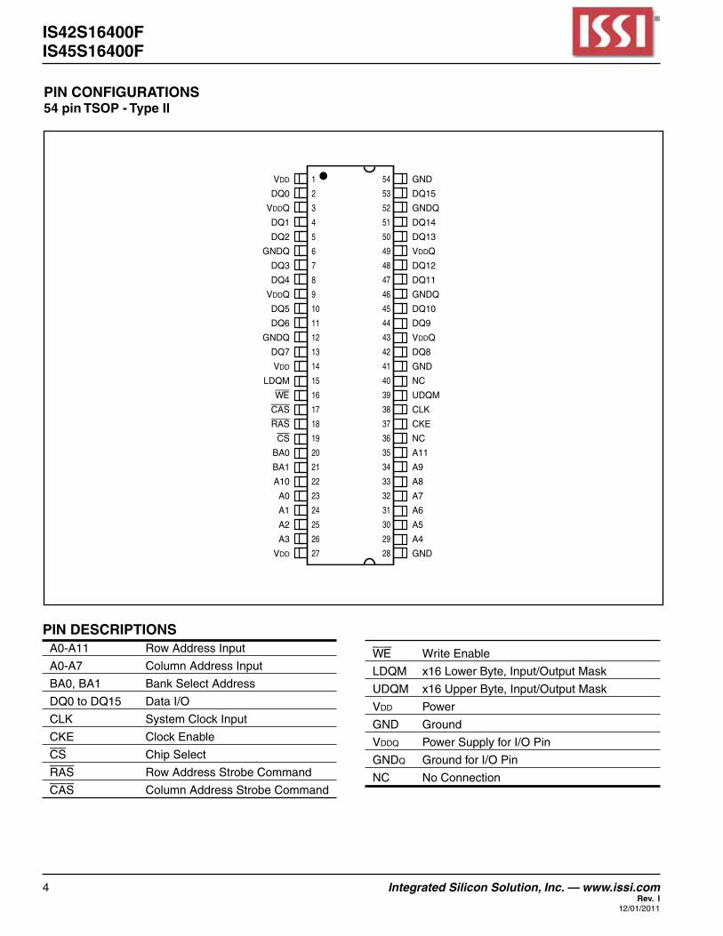
ReadandwriteaccessestotheSDRAMareburstoriented;accesses start at a selected location and continue fora programmed number of locations in a programmedsequence.AccessesbeginwiththeregistrationofanAC-TIVEcommandwhichisthenfollowedbyaREADorWRITEcommand.TheaddressbitsregisteredcoincidentwiththeACTIVEcommandareusedtoselectthebankandrowtobeaccessed(BA0andBA1selectthebank,A0-A11selecttherow).Theaddressbits(A0-A7)registeredcoincidentwiththeREADorWRITEcommandareusedtoselectthestartingcolumnlocationfortheburstaccess.

Prior to normal operation, the SDRAM must be initial-ized.Thefollowingsectionsprovidedetailedinformationcoveringdeviceinitialization,registerdefinition,commanddescriptionsanddeviceoperation.

InitializationSDRAMs must be powered up and initialized in apredefinedmanner.

The64MbSDRAMisinitializedafterthepowerisappliedtoVddandVddq(simultaneously),andtheclockisstablewithDQMHighandCKEHigh.

A100µsdelayisrequiredpriortoissuinganycommandotherthanaCOMMANDINHIBIToraNOP.TheCOMMANDINHIBITorNOPmaybeappliedduringthe100µsperiodandcontinueshouldatleastthroughtheendoftheperiod.

WithatleastoneCOMMANDINHIBITorNOPcommandhavingbeenapplied,aPRECHARGEcommandshouldbeappliedoncethe100µsdelayhasbeensatisfied.Allbanksmustbeprecharged.Thiswill leaveallbanksinanidlestate,afterwhichatleasttwoAUTOREFRESHcyclesmustbeperformed. AftertheAUTOREFRESHcyclesarecomplete, the SDRAM is then ready for mode registerprogramming.

The mode register should be loaded prior to applyinganyoperationalcommandbecauseitwillpowerupinanunknownstate.AftertheLoadModeRegistercommand,at least oneNOPcommandmust beassertedprior toanycommand.

18 Integrated Silicon Solution, Inc. — www.issi.com Rev. I

12/01/2011

IS42S16400FIS45S16400F

REGISTER DEFINITION

Mode RegisterThemode register isused todefine thespecificmodeofoperationof theSDRAM.Thisdefinition includestheselectionofaburstlength,abursttype,aCASlatency,anoperatingmodeandawriteburstmode,asshowninMODEREGISTERDEFINITION.

ThemoderegisterisprogrammedviatheLOADMODEREGISTERcommandandwillretainthestoredinformationuntilitisprogrammedagainorthedevicelosespower.

Mode register bitsM0-M2specify theburst length,M3specifiesthetypeofburst(sequentialorinterleaved),M4-M6specifytheCASlatency,M7andM8specifytheoperatingmode,M9specifiestheWRITEburstmode,andM10andM11arereservedforfutureuse.

Themode registermustbe loadedwhenallbanksareidle,andthecontrollermustwaitthespecifiedtimebeforeinitiatingthesubsequentoperation.Violatingeitheroftheserequirementswillresultinunspecifiedoperation.

MODE REGISTER DEFINITION

Latency Mode

M6 M5 M4 CAS Latency

0 0 0 Reserved 0 0 1 Reserved 0 1 0 2 0 1 1 3 1 0 0 Reserved 1 0 1 Reserved 1 1 0 Reserved 1 1 1 Reserved

1. To ensure compatibility with future devices,should program M11, M10 = "0, 0"

Write Burst Mode

M9 Mode

0 Programmed Burst Length

1 Single Location Access

Operating Mode

M8 M7 M6-M0 Mode

0 0 Defined Standard Operation — — — All Other States Reserved

Burst Type

M3 Type

0 Sequential 1 Interleaved

Burst Length

M2 M1 M0 M3=0 M3=1

0 0 0 1 1 0 0 1 2 2 0 1 0 4 4 0 1 1 8 8 1 0 0 Reserved Reserved 1 0 1 Reserved Reserved 1 1 0 Reserved Reserved 1 1 1 Full Page Reserved

Reserved

Address Bus

Mode Register (Mx)

A11 A10 A9 A8 A7 A6 A5 A4 A3 A2 A1 A0

(1)

Integrated Silicon Solution, Inc. — www.issi.com 19Rev. I12/01/2011

IS42S16400FIS45S16400F

BURST DEFINITION

Burst Starting Column Order of Accesses Within a Burst

Length Address Type = Sequential Type = Interleaved

A0

2 0 0-1 0-1

1 1-0 1-0

A1 A0

0 0 0-1-2-3 0-1-2-3

4 0 1 1-2-3-0 1-0-3-2

1 0 2-3-0-1 2-3-0-1

1 1 3-0-1-2 3-2-1-0

A2 A1 A0

0 0 0 0-1-2-3-4-5-6-7 0-1-2-3-4-5-6-7

0 0 1 1-2-3-4-5-6-7-0 1-0-3-2-5-4-7-6

0 1 0 2-3-4-5-6-7-0-1 2-3-0-1-6-7-4-5

8 0 1 1 3-4-5-6-7-0-1-2 3-2-1-0-7-6-5-4

1 0 0 4-5-6-7-0-1-2-3 4-5-6-7-0-1-2-3

1 0 1 5-6-7-0-1-2-3-4 5-4-7-6-1-0-3-2

1 1 0 6-7-0-1-2-3-4-5 6-7-4-5-2-3-0-1

1 1 1 7-0-1-2-3-4-5-6 7-6-5-4-3-2-1-0

Full n=A0-A7 Cn,Cn+1,Cn+2 NotSupported Page Cn+3,Cn+4... (y) (location0-y) …Cn-1, Cn…

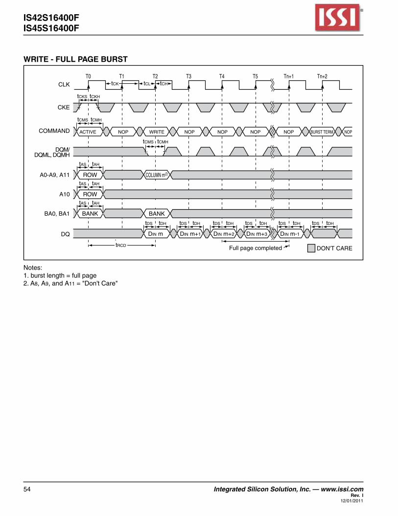
Burst LengthReadandwriteaccessestotheSDRAMareburstoriented,withtheburst lengthbeingprogrammable,asshowninMODEREGISTERDEFINITION.Theburstlengthdeter-minesthemaximumnumberofcolumnlocationsthatcanbeaccessedforagivenREADorWRITEcommand.Burstlengthsof1,2,4or8locationsareavailableforboththesequentialandtheinterleavedbursttypes,andafull-pageburst is available for the sequential type.The full-pageburstisusedinconjunctionwiththeBURSTTERMINATEcommandtogeneratearbitraryburstlengths.

Reservedstatesshouldnotbeused,asunknownoperationorincompatibilitywithfutureversionsmayresult.

WhenaREADorWRITEcommandisissued,ablockofcolumnsequaltotheburstlengthiseffectivelyselected.Allaccessesforthatbursttakeplacewithinthisblock,mean-

ingthattheburstwillwrapwithintheblockifaboundaryisreached.TheblockisuniquelyselectedbyA1-A7(x16)whentheburstlengthissettotwo;byA2-A7(x16)whentheburstlengthissettofour;andbyA3-A7(x16)whentheburstlengthissettoeight.Theremaining(leastsignificant)addressbit(s)is(are)usedtoselectthestartinglocationwithintheblock.Full-pageburstswrapwithinthepageiftheboundaryisreached.

Burst TypeAccesseswithinagivenburstmaybeprogrammedtobeeithersequentialorinterleaved;thisisreferredtoasthebursttypeandisselectedviabitM3.

Theorderingofaccesseswithinaburstisdeterminedbytheburstlength,thebursttypeandthestartingcolumnaddress,asshowninBURSTDEFINITIONtable.

20 Integrated Silicon Solution, Inc. — www.issi.com Rev. I

12/01/2011

IS42S16400FIS45S16400F

DON'T CARE

UNDEFINED

CLK

COMMAND

DQ

READ NOP NOP NOP

CAS Latency - 3

tAC

tOH

DOUT

T0 T1 T2 T3 T4

tLZ

CLK

COMMAND

DQ

READ NOP NOP

CAS Latency - 2

tAC

tOH

DOUT

T0 T1 T2 T3

tLZ

CAS Latency

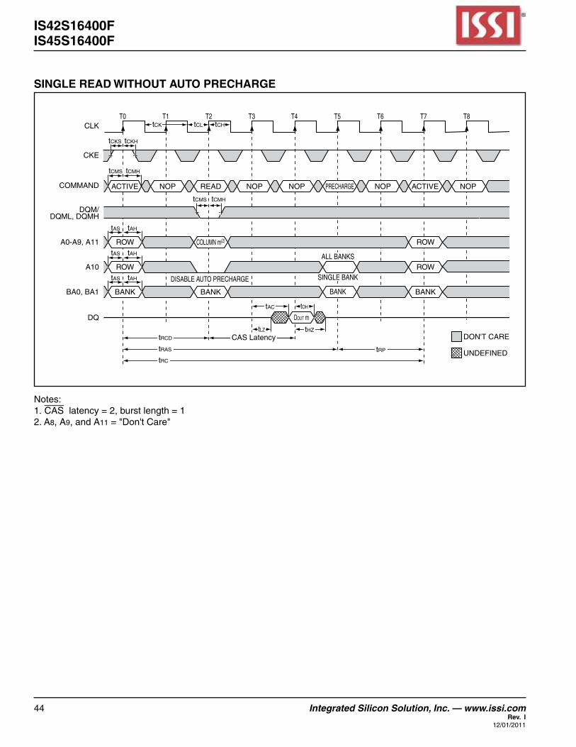
CAS LatencyTheCAS latency is thedelay, inclockcycles,betweentheregistrationofaREADcommandandtheavailabilityofthefirstpieceofoutputdata.Thelatencycanbesettotwoorthreeclocks.

IfaREADcommandisregisteredatclockedgen,andthelatencyism clocks,thedatawillbeavailablebyclockedgen + m.TheDQswillstartdrivingasaresultoftheclockedgeonecycleearlier(n + m -1),andprovidedthattherelevantaccesstimesaremet,thedatawillbevalidbyclockedgen + m.Forexample,assumingthattheclockcycletimeissuchthatallrelevantaccesstimesaremet,ifaREADcommandisregisteredatT0andthelatencyisprogrammedto twoclocks, theDQswillstartdrivingafterT1andthedatawillbevalidbyT2,asshowninCASLatencydiagrams.TheAllowable Operating FrequencytableindicatestheoperatingfrequenciesatwhicheachCASlatencysettingcanbeused.

Reservedstatesshouldnotbeusedasunknownoperationorincompatibilitywithfutureversionsmayresult.

CAS LatencyAllowable Operating Frequency (MHz)

Speed CAS Latency = 2 CAS Latency = 3

5 133 200

6 133 166

7 133 143

Operating ModeThenormaloperatingmodeisselectedbysettingM7andM8tozero;theothercombinationsofvaluesforM7andM8arereservedforfutureuseand/ortestmodes.TheprogrammedburstlengthappliestobothREADandWRITEbursts.

Testmodesandreservedstatesshouldnotbeusedbe-cause unknown operation or incompatibility with futureversionsmayresult.

Write Burst ModeWhenM9=0,theburstlengthprogrammedviaM0-M2appliestobothREADandWRITEbursts;whenM9=1,theprogrammedburstlengthappliestoREADbursts,butwriteaccessesaresingle-location(nonburst)accesses.

Integrated Silicon Solution, Inc. — www.issi.com 21Rev. I12/01/2011

IS42S16400FIS45S16400F

CLK

CKEHIGH

ROW ADDRESS

BANK ADDRESS

CS

RAS

CAS

WE

A0-A11

BA0, BA1

Activating Specific Row Within Specific Bank

DON'T CARE

CLK

COMMAND ACTIVE NOP NOP

tRCD

T0 T1 T2 T3 T4

READ orWRITE

OPERATION

BANK/ROW ACTIVATIONBeforeanyREADorWRITEcommandscanbe issuedtoabankwithintheSDRAM,arowinthatbankmustbe“opened.”ThisisaccomplishedviatheACTIVEcommand,whichselectsboththebankandtherowtobeactivated(seeActivatingSpecificRowWithinSpecificBank).

Afteropeningarow(issuinganACTIVEcommand),aREADorWRITEcommandmaybeissuedtothatrow,subjecttothetrcdspecification.Minimumtrcdshouldbedividedbytheclockperiodandroundeduptothenextwholenumberto determine the earliest clock edge after the ACTIVEcommandonwhichaREADorWRITEcommandcanbeentered.Forexample,atrcdspecificationof20nswitha125MHzclock(8nsperiod)resultsin2.5clocks,roundedto3.Thisisreflectedinthefollowingexample,whichcov-ersanycasewhere2<[trcd(MIN)/tck]≤3.(Thesameprocedureisusedtoconvertotherspecificationlimitsfromtimeunitstoclockcycles).

AsubsequentACTIVEcommandtoadifferentrowinthesamebankcanonlybeissuedafterthepreviousactiverowhasbeen“closed”(precharged).TheminimumtimeintervalbetweensuccessiveACTIVEcommands to thesamebankisdefinedbytrc.

AsubsequentACTIVEcommandtoanotherbankcanbeissuedwhilethefirstbankisbeingaccessed,whichresultsinareductionoftotalrow-accessoverhead.TheminimumtimeintervalbetweensuccessiveACTIVEcommandstodifferentbanksisdefinedbytrrd.

Example: Meeting tRCD (MIN) when 2 < [tRCD (min)/tCK] ≤ 3

22 Integrated Silicon Solution, Inc. — www.issi.com Rev. I

12/01/2011

IS42S16400FIS45S16400F

CLK

CKEHIGH

COLUMN ADDRESS

AUTO PRECHARGE

NO PRECHARGE

CS

RAS

CAS

WE

A0-A7

A10

BA0, BA1 BANK ADDRESS

A8, A9, A11

READ COMMANDREADSREAD bursts are initiated with a READ command, asshownintheREADCOMMANDdiagram.

ThestartingcolumnandbankaddressesareprovidedwiththeREADcommand,andautoprechargeiseitherenabledordisabledforthatburstaccess.Ifautoprechargeisenabled,therowbeingaccessedisprechargedatthecompletionoftheburst.ForthegenericREADcommandsusedinthefol-lowingillustrations,autoprechargeisdisabled.

DuringREADbursts,thevaliddata-outelementfromthestarting column address will be available following theCASlatencyaftertheREADcommand.Eachsubsequentdata-outelementwillbevalidbythenextpositiveclockedge.TheCASLatencydiagramshowsgeneral timingforeachpossibleCASlatencysetting.

Uponcompletionofaburst,assumingnoothercommandshavebeeninitiated,theDQswillgoHigh-Z.Afull-pageburstwillcontinueuntilterminated.(Attheendofthepage,itwillwraptocolumn0andcontinue.)

DatafromanyREADburstmaybetruncatedwithasub-sequentREADcommand,anddatafromafixed-lengthREADburstmaybeimmediatelyfollowedbydatafromaREADcommand.Ineithercase,acontinuousflowofdatacanbemaintained.Thefirstdataelementfromthenewburstfollowseitherthelastelementofacompletedburstorthelastdesireddataelementofalongerburstwhichisbeingtruncated.

ThenewREADcommandshouldbeissuedx cyclesbeforetheclockedgeatwhichthelastdesireddataelementisvalid,wherex equalstheCASlatencyminusone.ThisisshowninConsecutiveREADBurstsforCASlatenciesoftwoandthree;dataelementn +3iseitherthelastofaburstoffourorthelastdesiredofalongerburst.The64MbSDRAMusesapipelinedarchitectureandthereforedoesnotrequirethe2n ruleassociatedwithaprefetcharchitec-ture.AREADcommandcanbeinitiatedonanyclockcyclefollowingapreviousREADcommand.Full-speedrandomreadaccessescanbeperformedtothesamebank,asshowninRandomREADAccesses,oreachsubsequentREADmaybeperformedtoadifferentbank.

DatafromanyREADburstmaybetruncatedwithasub-sequent WRITE command, and data from a fixed-lengthREADburstmaybeimmediatelyfollowedbydatafromaWRITEcommand(subjecttobusturnaroundlimitations).TheWRITEburstmaybeinitiatedontheclockedgeim-mediatelyfollowingthelast(orlastdesired)dataelementfromtheREADburst,providedthatI/Ocontentioncanbeavoided.Inagivensystemdesign,theremaybeapos-sibilitythatthedevicedrivingtheinputdatawillgoLow-ZbeforetheSDRAMDQsgoHigh-Z.Inthiscase,atleastasingle-cycledelayshouldoccurbetweenthelastreaddataandtheWRITEcommand.

TheDQMinputisusedtoavoidI/Ocontention,asshowninFiguresRW1andRW2.TheDQMsignalmustbeas-serted (HIGH)at least threeclocksprior to theWRITEcommand(DQMlatencyistwoclocksforoutputbuffers)tosuppressdata-out fromtheREAD.Once theWRITEcommandisregistered,theDQswillgoHigh-Z(orremainHigh-Z),regardlessofthestateoftheDQMsignal,providedtheDQMwasactiveontheclockjustpriortotheWRITEcommandthattruncatedtheREADcommand.Ifnot,thesecondWRITEwillbeaninvalidWRITE.Forexample,ifDQMwasLOWduringT4inFigureRW2,thentheWRITEsatT5andT7wouldbevalid,whiletheWRITEatT6wouldbeinvalid.

TheDQMsignalmustbede-assertedpriortotheWRITEcommand(DQMlatencyiszeroclocksforinputbuffers)toensurethatthewrittendataisnotmasked.

Afixed-lengthREADburstmaybefollowedby,ortruncatedwith,aPRECHARGEcommandtothesamebank(providedthatautoprechargewasnotactivated),andafull-pageburstmaybetruncatedwithaPRECHARGEcommandtothesamebank.ThePRECHARGEcommandshouldbeissuedx cyclesbeforetheclockedgeatwhichthelastdesireddataelement isvalid,wherex equals theCAS latencyminusone.ThisisshownintheREADtoPRECHARGE

Integrated Silicon Solution, Inc. — www.issi.com 23Rev. I12/01/2011

IS42S16400FIS45S16400F

DON'T CARE

UNDEFINED

CLK

COMMAND

DQ

READ NOP NOP NOP

CAS Latency - 3

tAC

tOH

DOUT

T0 T1 T2 T3 T4

tLZ

CLK

COMMAND

DQ

READ NOP NOP

CAS Latency - 2

tAC

tOH

DOUT

T0 T1 T2 T3

tLZ

CAS Latency

diagramforeachpossibleCASlatency;dataelementn +3iseitherthelastofaburstoffourorthelastdesiredofalongerburst.FollowingthePRECHARGEcommand,asubsequentcommandtothesamebankcannotbeissueduntiltrpismet.Notethatpartoftherowprechargetimeishiddenduringtheaccessofthelastdataelement(s).

In the case of a fixed-length burst being executed tocompletion, a PRECHARGE command issued at theoptimum time (asdescribedabove)provides thesameoperation that would result from the same fixed-lengthburstwithautoprecharge.ThedisadvantageofthePRE-CHARGEcommandisthatitrequiresthatthecommandandaddressbusesbeavailableattheappropriatetimetoissuethecommand;theadvantageofthePRECHARGEcommandisthatitcanbeusedtotruncatefixed-lengthorfull-pagebursts.

Full-pageREADburstscanbetruncatedwiththeBURSTTERMINATE command, and fixed-length READ burstsmaybetruncatedwithaBURSTTERMINATEcommand,providedthatautoprechargewasnotactivated.TheBURSTTERMINATEcommandshouldbeissuedx cyclesbeforetheclockedgeatwhichthelastdesireddataelementisvalid,wherex equalstheCASlatencyminusone.ThisisshownintheREADBurstTerminationdiagramforeachpossibleCASlatency;dataelementn +3isthelastdesireddataelementofalongerburst.

24 Integrated Silicon Solution, Inc. — www.issi.com Rev. I

12/01/2011

IS42S16400FIS45S16400F

DON'T CARE

CLK

COMMAND

ADDRESS

DQ

T0 T1 T2 T3 T4 T5 T6

READ NOP NOP NOP READ NOP NOP

DOUT n DOUT n+1 DOUT n+2 DOUT n+3 DOUT b

BANK,COL n

BANK,COL b

CAS Latency - 2

x = 1 cycle

DON'T CARE

CLK

COMMAND

ADDRESS

DQ

T0 T1 T2 T3 T4 T5 T6 T7

READ NOP NOP NOP READ NOP NOP NOP

DOUT n DOUT n+1 DOUT n+2 DOUT n+3 DOUT b

BANK,COL n

BANK,COL b

CAS Latency - 3

x = 2 cycles

Consecutive READ Bursts

Integrated Silicon Solution, Inc. — www.issi.com 25Rev. I12/01/2011

IS42S16400FIS45S16400F

DON'T CARE

CLK

COMMAND

ADDRESS

DQ

T0 T1 T2 T3 T4 T5

READ READ READ READ NOP NOP

DOUT n DOUT b DOUT m DOUT x

BANK,COL n

BANK,COL b

CAS Latency - 2

BANK,COL m

BANK,COL x

DON'T CARE

CLK

COMMAND

ADDRESS

DQ

T0 T1 T2 T3 T4 T5 T6

READ READ READ READ NOP NOP NOP

DOUT n DOUT b DOUT m DOUT x

BANK,COL n

BANK,COL b

CAS Latency - 3

BANK,COL m

BANK,COL x

Random READ Accesses

26 Integrated Silicon Solution, Inc. — www.issi.com Rev. I

12/01/2011

IS42S16400FIS45S16400F

DON'T CARE

CLK

DQM

COMMAND

ADDRESS

DQ

T0 T1 T2 T3 T4 T5

READ NOP NOP NOP NOP WRITE

BANK,COL n

BANK,COL b

DOUT n DIN b

tDS

tHZ

CAS Latency - 3

RW1 - READ to WRITE

RW2 - READ to WRITE

DON'T CARE

CLK

DQM

COMMAND

ADDRESS

DQ

T0 T1 T2 T3 T4 T5 T6

READ NOP NOP NOP NOP NOP WRITE

BANK,COL n

DIN b

tDS

tHZ

BANK,COL b

CAS Latency - 2

DOUT n DOUT n+1 DOUT n+2

Integrated Silicon Solution, Inc. — www.issi.com 27Rev. I12/01/2011

IS42S16400FIS45S16400F

DON'T CARE

CLK

COMMAND

ADDRESS

DQ

T0 T1 T2 T3 T4 T5 T6 T7

READ NOP NOP NOP NOP NOP ACTIVE

DOUT n DOUT n+1 DOUT n+2 DOUT n+3

BANK a,COL n

BANK a,ROW

BANK(a or all)

CAS Latency - 2

x = 1 cycle

tRP

PRECHARGE

DON'T CARE

CLK

COMMAND

ADDRESS

DQ

T0 T1 T2 T3 T4 T5 T6 T7

READ NOP NOP NOP NOP NOP ACTIVE

DOUT n DOUT n+1 DOUT n+2 DOUT n+3

BANK,COL n

BANK,COL b

CAS Latency - 3

x = 2 cycles

tRP

BANK a,ROW

PRECHARGE

READ to PRECHARGE

28 Integrated Silicon Solution, Inc. — www.issi.com Rev. I

12/01/2011

IS42S16400FIS45S16400F

DON'T CARE

CLK

COMMAND

ADDRESS

DQ

T0 T1 T2 T3 T4 T5 T6

READ NOP NOP NOP NOP NOP

DOUT n DOUT n+1 DOUT n+2 DOUT n+3

BANK a,COL n

CAS Latency - 2

x = 1 cycle

BURSTTERMINATE

DON'T CARE

CLK

COMMAND

ADDRESS

DQ

T0 T1 T2 T3 T4 T5 T6 T7

READ NOP NOP NOP NOP NOP NOP

DOUT n DOUT n+1 DOUT n+2 DOUT n+3

BANK,COL n

CAS Latency - 3

x = 2 cycles

BURSTTERMINATE

READ Burst Termination

Integrated Silicon Solution, Inc. — www.issi.com 29Rev. I12/01/2011

IS42S16400FIS45S16400F

CLK

CKEHIGH

COLUMN ADDRESS

AUTO PRECHARGE

BANK ADDRESS

CS

RAS

CAS

WE

A0-A7

A10

BA0, BA1

NO PRECHARGE

A8, A9, A11

WRITE Command

ThestartingcolumnandbankaddressesareprovidedwiththeWRITEcommand,andautoprechargeiseitherenabledordisabledforthataccess.Ifautoprechargeisenabled,therowbeingaccessedisprechargedatthecompletionoftheburst.ForthegenericWRITEcommandsusedinthefollowingillustrations,autoprechargeisdisabled.

DuringWRITEbursts,thefirstvaliddata-inelementwillberegisteredcoincidentwiththeWRITEcommand.Subsequentdataelementswillberegisteredoneachsuccessiveposi-tiveclockedge.Uponcompletionofafixed-lengthburst,assumingnoother commandshavebeen initiated, theDQswillremainHigh-Zandanyadditionalinputdatawillbeignored(seeWRITEBurst).Afull-pageburstwillcon-tinueuntilterminated.(Attheendofthepage,itwillwraptocolumn0andcontinue.)

DataforanyWRITEburstmaybetruncatedwithasubse-quentWRITEcommand,anddataforafixed-lengthWRITEburstmaybe immediately followedbydata foraWRITEcommand.ThenewWRITEcommandcanbe issuedonanyclockfollowingthepreviousWRITEcommand,andthedataprovidedcoincidentwiththenewcommandappliestothenewcommand.

AnexampleisshowninWRITEtoWRITEdiagram.Datan +1iseitherthelastofaburstoftwoorthelastdesiredof a longer burst.The 64Mb SDRAM uses a pipelinedarchitectureandthereforedoesnotrequirethe2n ruleas-sociatedwithaprefetcharchitecture.AWRITEcommandcanbeinitiatedonanyclockcyclefollowingapreviousWRITEcommand.Full-speedrandomwriteaccesseswithinapagecanbeperformedtothesamebank,asshowninRandomWRITECycles,oreachsubsequentWRITEmaybeperformedtoadifferentbank.

DataforanyWRITEburstmaybetruncatedwithasubse-quentREADcommand,anddataforafixed-lengthWRITEburstmaybeimmediatelyfollowedbyasubsequentREADcommand.OncetheREADcommandisregistered,thedatainputswillbeignored,andWRITEswillnotbeex-ecuted.AnexampleisshowninWRITEtoREAD.Datan +1iseitherthelastofaburstoftwoorthelastdesiredofalongerburst.

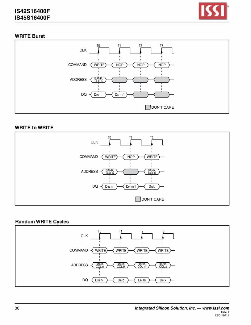
Data for a fixed-length WRITE burst may be followedby,or truncatedwith,aPRECHARGEcommandto thesamebank(providedthatautoprechargewasnotacti-vated), anda full-pageWRITEburstmaybe truncatedwithaPRECHARGEcommand to thesamebank.ThePRECHARGEcommandshouldbeissuedtwraftertheclockedgeatwhichthelastdesiredinputdataelementisregistered.Theautoprechargemoderequiresatwrofatleastoneclockplustime,regardlessoffrequency.Inaddition,whentruncatingaWRITEburst,theDQMsignalmustbeusedtomaskinputdatafortheclockedgepriorto,andtheclockedgecoincidentwith,thePRECHARGEcommand.AnexampleisshownintheWRITEtoPRE-CHARGEdiagram.Datan+1iseitherthelastofaburstoftwoorthelastdesiredofalongerburst.FollowingthePRECHARGEcommand,asubsequentcommandtothesamebankcannotbeissueduntiltrpismet.

Inthecaseofafixed-lengthburstbeingexecutedtocomple-tion,aPRECHARGEcommand issuedat theoptimumtime(asdescribedabove)providesthesameoperationthatwouldresult fromthesamefixed-lengthburstwithautoprecharge.ThedisadvantageofthePRECHARGEcommandisthatitrequiresthatthecommandandaddressbusesbeavailableattheappropriatetimetoissuethecommand;theadvantageofthePRECHARGEcommandisthatitcanbeusedtotruncatefixed-lengthorfull-pagebursts.

Fixed-lengthorfull-pageWRITEburstscanbetruncatedwiththeBURSTTERMINATEcommand.Whentruncat-ingaWRITEburst,theinputdataappliedcoincidentwiththeBURSTTERMINATEcommandwillbeignored.Thelastdatawritten(providedthatDQMisLOWatthattime)willbe the inputdataappliedoneclockpreviousto theBURSTTERMINATEcommand.ThisisshowninWRITEBurstTermination,wheredatan isthelastdesireddataelementofalongerburst.

WRITEsWRITEburstsareinitiatedwithaWRITEcommand,asshowninWRITECommanddiagram.

30 Integrated Silicon Solution, Inc. — www.issi.com Rev. I

12/01/2011

IS42S16400FIS45S16400F

CLK

COMMAND

ADDRESS

DQ

T0 T1 T2 T3

WRITE NOP NOP NOP

DIN n DIN n+1

BANK,COL n

DON'T CARE

CLK

COMMAND

ADDRESS

DQ

T0 T1 T2

WRITE NOP WRITE

DIN n DIN n+1 DIN b

BANK,COL n

BANK,COL b

DON'T CARE

WRITE Burst

WRITE to WRITE

CLK

COMMAND

ADDRESS

DQ

T0 T1 T2 T3

WRITE WRITE WRITE WRITE

DIN n DIN b DIN m DIN x

BANK,COL n

BANK,COL b

BANK,COL m

BANK,COL x

Random WRITE Cycles

Integrated Silicon Solution, Inc. — www.issi.com 31Rev. I12/01/2011

IS42S16400FIS45S16400F

DON'T CARE

CLK

COMMAND

ADDRESS

DQ

T0 T1 T2 T3 T4 T5

WRITE NOP READ NOP NOP NOP

DIN n DIN n+1 DOUT b DOUT b+1

BANK,COL n

BANK,COL b

CAS Latency - 2

WRITE to READ

WP1 - WRITE to PRECHARGE

DON'T CARE

CLK

DQM

COMMAND

ADDRESS

DQ

T0 T1 T2 T3 T4 T5 T6

WRITE NOP NOP ACTIVE NOP NOP

BANK a,COL n

BANK a,ROW

BANK(a or all)

tWR

tRP

PRECHARGE

DIN n DIN n+1

CAS Latency - 2

32 Integrated Silicon Solution, Inc. — www.issi.com Rev. I

12/01/2011

IS42S16400FIS45S16400F

CLK

COMMAND

ADDRESS

DQ

T0 T1 T2

WRITE

DIN n (DATA)

BANK,COL n

DON'T CARE

(ADDRESS)

BURSTTERMINATE

NEXTCOMMAND

WRITE Burst Termination

DON'T CARE

CLK

DQM

COMMAND

ADDRESS

DQ

T0 T1 T2 T3 T4 T5 T6

WRITE NOP NOP NOP ACTIVE NOP

BANK a,COL n

BANK a,ROW

BANK(a or all)

tWR

tRP

PRECHARGE

DIN n DIN n+1

CAS Latency - 3

WP2 - WRITE to PRECHARGE

Integrated Silicon Solution, Inc. — www.issi.com 33Rev. I12/01/2011

IS42S16400FIS45S16400F

CLK

CKEHIGH

ALL BANKS

BANK SELECT

BANK ADDRESS

CS

RAS

CAS

WE

A0-A9, A11

A10

BA0, BA1

DON'T CARE

CLK

CKE

COMMAND NOP NOP ACTIVE

≥ tCKStCKS

All banks idle

Enter power-down mode Exit power-down mode

tRCD

tRAS

tRC

Input buffers gated off

PRECHARGE Command

POWER-DOWN

POWER-DOWNPower-downoccursifCKEisregisteredLOWcoincidentwithaNOPorCOMMANDINHIBITwhennoaccessesareinprogress.Ifpower-downoccurswhenallbanksareidle,thismodeisreferredtoasprechargepower-down;ifpower-downoccurswhenthereisarowactiveineitherbank, this mode is referred to as active power-down.Entering power-down deactivates the input and outputbuffers,excludingCKE,formaximumpowersavingswhileinstandby.Thedevicemaynotremaininthepower-downstatelongerthantherefreshperiod(64ms)sincenorefreshoperationsareperformedinthismode.

Thepower-downstateisexitedbyregisteringaNOPorCOMMANDINHIBITandCKEHIGHatthedesiredclockedge(meetingtcks).Seefigurebelow.

PRECHARGEThePRECHARGEcommand(seefigure)isusedtodeac-tivatetheopenrowinaparticularbankortheopenrowinallbanks.Thebank(s)willbeavailableforasubsequentrowaccesssomespecifiedtime(trp)afterthePRECHARGEcommandisissued.InputA10determineswhetheroneorallbanksaretobeprecharged,andinthecasewhereonlyonebankistobeprecharged,inputsBA0,BA1selectthebank.Whenallbanksaretobeprecharged,inputsBA0,BA1aretreatedas“Don’tCare.”Onceabankhasbeenprecharged,it isintheidlestateandmustbeactivatedpriortoanyREADorWRITEcommandsbeingissuedtothatbank.

34 Integrated Silicon Solution, Inc. — www.issi.com Rev. I

12/01/2011

IS42S16400FIS45S16400F

DON'T CARE

CLK

CKE

COMMAND

ADDRESS

DQ

T0 T1 T2 T3 T4 T5

NOP WRITE NOP NOP

BANK a,COL n

DIN n DIN n+1 DIN n+2

INTERNALCLOCK

DON'T CARE

CLK

CKE

COMMAND

ADDRESS

DQ

T0 T1 T2 T3 T4 T5 T6

READ NOP NOP NOP NOP NOP

BANK a,COL n

DOUT n DOUT n+1 DOUT n+2 DOUT n+3

INTERNALCLOCK

CLOCK SUSPENDClocksuspendmodeoccurswhenacolumnaccess/burstis inprogressandCKEisregisteredLOW.In theclocksuspendmode,theinternalclockisdeactivated,“freezing”thesynchronouslogic.

ForeachpositiveclockedgeonwhichCKEissampledLOW,thenextinternalpositiveclockedgeissuspended.Anycommandordatapresentontheinputpinsatthetime

ofasuspendedinternalclockedgeisignored;anydatapresentontheDQpinsremainsdriven;andburstcountersarenotincremented,aslongastheclockissuspended.(Seefollowingexamples.)

ClocksuspendmodeisexitedbyregisteringCKEHIGH;theinternalclockandrelatedoperationwillresumeonthesubsequentpositiveclockedge.

Clock Suspend During WRITE Burst

Clock Suspend During READ Burst

Integrated Silicon Solution, Inc. — www.issi.com 35Rev. I12/01/2011

IS42S16400FIS45S16400F

DON'T CARE

CLK

COMMAND

BANK n

BANK m

ADDRESS

DQ

T0 T1 T2 T3 T4 T5 T6 T7

NOP NOP NOP NOP NOP NOP

DOUT a DOUT a+1 DOUT b DOUT b+1

BANK n,COL a

BANK m,COL b

CAS Latency - 3 (BANK n)

CAS Latency - 3 (BANK m)

tRP - BANK n tRP - BANK m

READ - APBANK n

READ - APBANK m

Page Active READ with Burst of 4 Interrupt Burst, Precharge Idle

Page Active READ with Burst of 4 Precharge

Internal States

DON'T CARE

CLK

COMMAND

BANK n

BANK m

ADDRESS

DQM

DQ

T0 T1 T2 T3 T4 T5 T6 T7

NOP NOP NOP NOP NOP NOP

DOUT a DIN b DIN b+1 DIN b+2 DIN b+3

BANK n,COL a

BANK m,COL b

CAS Latency - 3 (BANK n)

tRP - BANK n tRP - BANK m

WRITE - APBANK n

WRITE - APBANK m

READ with Burst of 4 Interrupt Burst, Precharge Idle

Page Active WRITE with Burst of 4 Write-Back

Internal States Page Active

BURST READ/SINGLE WRITETheburstread/singlewritemodeisenteredbyprogrammingthewriteburstmodebit(M9)inthemoderegistertoalogic1.Inthismode,allWRITEcommandsresultintheaccessofasinglecolumnlocation(burstofone),regardlessoftheprogrammedburstlength.READcommandsaccesscolumnsaccordingtotheprogrammedburstlengthandsequence,justasinthenormalmodeofoperation(M9=0).

CONCURRENT AUTO PRECHARGEAnaccesscommand(READorWRITE)toanotherbankwhileanaccesscommandwithautoprechargeenabledisexecutingisnotallowedbySDRAMs,unlesstheSDRAMsupports CONCURRENT AUTO PRECHARGE. ISSI

SDRAMssupportCONCURRENTAUTOPRECHARGE.FourcaseswhereCONCURRENTAUTOPRECHARGEoccursaredefinedbelow.

READ with Auto Precharge1.InterruptedbyaREAD(withorwithoutautoprecharge):

AREADtobankmwill interruptaREADonbankn,CAS latency later.The PRECHARGE to bank n willbeginwhentheREADtobankmisregistered.

2.InterruptedbyaWRITE(withorwithoutautoprecharge):AWRITEtobankmwillinterruptaREADonbanknwhenregistered.DQMshouldbeusedtwoclockspriortotheWRITEcommandtopreventbuscontention.ThePRECHARGEtobanknwillbeginwhentheWRITEtobankmisregistered.

Fig CAP 1 - READ With Auto Precharge interrupted by a READ

Fig CAP 2 - READ With Auto Precharge interrupted by a WRITE

36 Integrated Silicon Solution, Inc. — www.issi.com Rev. I

12/01/2011

IS42S16400FIS45S16400F

DON'T CARE

CLK

COMMAND

BANK n

BANK m

ADDRESS

DQ

T0 T1 T2 T3 T4 T5 T6 T7

NOP NOP NOP NOP NOP NOP

DIN a DIN a+1 DOUT b DOUT b+1

BANK n,COL a

BANK m,COL b

CAS Latency - 3 (BANK m)

tRP - BANK ntRP - BANK m

WRITE - APBANK n

READ - APBANK m

Page Active WRITE with Burst of 4 Interrupt Burst, Write-Back Precharge

Page Active READ with Burst of 4 Precharge

Internal States tWR - BANK n

DON'T CARE

CLK

COMMAND

BANK n

BANK m

ADDRESS

DQ

T0 T1 T2 T3 T4 T5 T6 T7

NOP NOP NOP NOP NOP NOP

BANK n,COL a

BANK m,COL b

tRP - BANK ntRP - BANK m

WRITE - APBANK n

WRITE - APBANK m

Page Active WRITE with Burst of 4 Interrupt Burst, Write-Back Precharge

Page Active WRITE with Burst of 4 Write-Back

Internal States tWR - BANK n

DIN a DIN a+1 DIN a+2 DIN b DIN b+1 DIN b+2 DIN b+3

WRITE with Auto Precharge3.InterruptedbyaREAD(withorwithoutautoprecharge):

AREADtobankmwill interruptaWRITEonbanknwhenregistered,withthedata-outappearingCASlatencylater.ThePRECHARGEtobanknwillbeginaftertwrismet,wheretwrbeginswhentheREADtobankmisregistered.ThelastvalidWRITEtobanknwillbedata-inregisteredoneclockpriortotheREADtobankm.

4.InterruptedbyaWRITE(withorwithoutautoprecharge):AWRITEtobankmwillinterruptaWRITEonbanknwhenregistered.ThePRECHARGEtobanknwillbeginaftertwrismet,wheretwrbeginswhentheWRITEtobankmisregistered.ThelastvaliddataWRITEtobanknwillbedataregisteredoneclockpriortoaWRITEtobankm.

Fig CAP 3 - WRITE With Auto Precharge interrupted by a READ

Fig CAP 4 - WRITE With Auto Precharge interrupted by a WRITE

Integrated Silicon Solution, Inc. — www.issi.com 37Rev. I12/01/2011

IS42S16400FIS45S16400F

INITIALIzE AND LOAD MODE REGISTER(1)

Notes:1.IfCSisHighatclockHightime,allcommandsappliedareNOP.2.TheModeregistermaybeloadedpriortotheAuto-Refreshcyclesifdesired.3.JEDECandPC100specifythreeclocks.4.OutputsareguaranteedHigh-Zafterthecommandisissued.

DON'T CARE

CLK

CKE

COMMAND

DQM/DQML, DQMH

A0-A9, A11

A10

BA0, BA1

DQ

tCH tCLtCK

tCMS tCMH tCMS tCMH tCMS tCMH

tCKS tCKH

T0 T1 Tn+1 To+1 Tp+1 Tp+2 Tp+3

tMRDtRCtRCtRP

ROW

ROW

BANK

tAS tAH

tAS tAH

CODE

CODEALL BANKS

SINGLE BANK

ALL BANKS

AUTOREFRESH

AUTOREFRESH

Load MODEREGISTER

T = 100µs Min.

Power-up: VCC

and CLK stablePrechargeall banks

AUTO REFRESH Program MODE REGISTER

NOP PRECHARGE NOP NOP NOP ACTIVE

T

(2, 3, 4)AUTO REFRESH

At least 2 Auto-Refresh Commands

38 Integrated Silicon Solution, Inc. — www.issi.com Rev. I

12/01/2011

IS42S16400FIS45S16400F

POWER-DOWN MODE CYCLE

CASlatency=2,3

DON'T CARE

CLK

CKE

COMMAND

DQM/DQML, DQMH

A0-A9, A11

A10

BA0, BA1

DQ

tAS tAH

BANK

tCHtCLtCK

tCMS tCMH

tCKS tCKH

PRECHARGE NOP NOP NOP ACTIVE

ALL BANKS

SINGLE BANK

ROW

ROW

BANK

tCKStCKS

Precharge allactive banks

All banks idleTwo clock cycles Input buffers gatedoff while in

power-down modeAll banks idle, enterpower-down mode Exit power-down mode

T0 T1 T2 Tn+1 Tn+2

High-Z

Integrated Silicon Solution, Inc. — www.issi.com 39Rev. I12/01/2011

IS42S16400FIS45S16400F

CLOCK SUSPEND MODE

Notes:1.CASlatency=3,burstlength=22.A8,A9,andA11="Don'tCare"

DON'T CARE

CLK

CKE

COMMAND

DQM/DQML, DQMH

A0-A9, A11

A10

BA0, BA1

DQ

tCMS tCMH

tAS tAH

tAS tAH

tAS tAH

tCHtCLtCK

tCMS tCMH

tCKS tCKH

COLUMN m(2)

T0 T1 T2 T3 T4 T5 T6 T7 T8 T9

READ NOP NOP NOP NOP NOP WRITE NOP

tCKS tCKH

BANK BANK

COLUMN n(2)

tAC tAC

tOH

tHZ

DOUT m DOUT m+1

tLZ

UNDEFINED

DOUT e+1

tDS tDH

DOUT e

40 Integrated Silicon Solution, Inc. — www.issi.com Rev. I

12/01/2011

IS42S16400FIS45S16400F

AUTO-REFRESH CYCLE

CASlatency=2,3

tRP tRC tRC

DON'T CARE

CLK

CKE

COMMAND

DQM/DQML, DQMH

A0-A9, A11

A10

BA0, BA1

DQ

tAS tAH

tCHtCLtCK

tCMS tCMH

tCKS tCKH

T0 T1 T2 Tn+1 To+1

ALL BANKS

SINGLE BANK

BANK(s)

ROW

ROW

BANK

High-Z

PRECHARGE NOP NOP NOP ACTIVEAutoRefresh

AutoRefresh

Integrated Silicon Solution, Inc. — www.issi.com 41Rev. I12/01/2011

IS42S16400FIS45S16400F

SELF-REFRESH CYCLE

Note:1.Self-RefreshModeisnotsupportedforA2gradewithTa>85oC.

CLK

CKE

COMMAND

DQM/DQML, DQMH

A0-A9, A11

A10

BA0, BA1

DQ

tAS tAH

BANK

tCLtCHtCK

tCMS tCMH

tCKS tCKH

ALL BANKS

SINGLE BANK

tCKS

Precharge allactive banks

CLK stable prior to exitingself refresh mode

Enter selfrefresh mode

Exit self refresh mode(Restart refresh time base)

T0 T1 T2 Tn+1 To+1 To+2

High-Z

AutoRefresh

AutoRefreshPRECHARGE NOP NOP NOP

tCKS

≥ tRAS

tRP tXSR

DON'T CARE

42 Integrated Silicon Solution, Inc. — www.issi.com Rev. I

12/01/2011

IS42S16400FIS45S16400F

READ WITHOUT AUTO PRECHARGE

DON'T CARE

UNDEFINED

CLK

CKE

COMMAND

DQM/DQML, DQMH

A0-A9, A11

A10

BA0, BA1

DQ

tCMS tCMH

ACTIVE NOP READ NOP NOP NOP PRECHARGE NOP ACTIVE

tAS tAH

tAS tAH

tAS tAH

ROW

ROW

BANK

COLUMN m(2)

tCHtCLtCK

tCMS tCMH

tCKS tCKH

BANK

tRCD CAS Latency

tAC tAC tAC tAC

tOH

tHZ

tOH

DOUT m

tOH

DOUT m+1

tOH

DOUT m+2 DOUT m+3

T0 T1 T2 T3 T4 T5 T6 T7 T8

DISABLE AUTO PRECHARGE

ROW

ROW

BANK

tLZ

tRAS

tRC

tRP

ALL BANKS

SINGLE BANK

BANK

Notes:1.CASlatency=2,burstlength=42.A8,A9,andA11="Don'tCare"

Integrated Silicon Solution, Inc. — www.issi.com 43Rev. I12/01/2011

IS42S16400FIS45S16400F

READ WITH AUTO PRECHARGE

DON'T CARE

UNDEFINED

CLK

CKE

COMMAND

DQM/DQML, DQMH

A0-A9, A11

A10

BA0, BA1

DQ

tCMS tCMH

ACTIVE NOP READ NOP NOP NOP NOP NOP ACTIVE

tAS tAH

tAS tAH

tAS tAH

ROW

ROW

BANK

COLUMN m(2)

tCHtCLtCK

tCMS tCMH

tCKS tCKH

BANK

tRCD

tRAS

tRC

CAS Latency

tAC tAC tAC tAC

tOH

tHZ

tOH

DOUT m

tOH

DOUT m+1

tOH

DOUT m+2 DOUT m+3

T0 T1 T2 T3 T4 T5 T6 T7 T8

tRP

ENABLE AUTO PRECHARGE

ROW

ROW

BANK

tLZ

Notes:1.CASlatency=2,burstlength=42.A8,A9,andA11="Don'tCare"

44 Integrated Silicon Solution, Inc. — www.issi.com Rev. I

12/01/2011

IS42S16400FIS45S16400F

SINGLE READ WITHOUT AUTO PRECHARGE

DON'T CARE

UNDEFINED

CLK

CKE

COMMAND

DQM/DQML, DQMH

A0-A9, A11

A10

BA0, BA1

DQ

tCMS tCMH

ACTIVE NOP READ NOP NOP PRECHARGE NOP ACTIVE NOP

tAS tAH

tAS tAH

tAS tAH

ROW

ROW

BANK

COLUMN m(2)

tCHtCLtCK

tCMS tCMH

tCKS tCKH

BANK

tRCD

tRAS

tRC

CAS Latency

tAC

tHZ

tOH

DOUT m

T0 T1 T2 T3 T4 T5 T6 T7 T8

tRP

DISABLE AUTO PRECHARGE

ROW

ROW

BANK

tLZ

ALL BANKS

SINGLE BANK

BANK

Notes:1.CASlatency=2,burstlength=12.A8,A9,andA11="Don'tCare"

Integrated Silicon Solution, Inc. — www.issi.com 45Rev. I12/01/2011

IS42S16400FIS45S16400F

SINGLE READ WITH AUTO PRECHARGE

DON'T CARE

UNDEFINED

CLK

CKE

COMMAND

DQM/DQML, DQMH

A0-A9, A11

A10

BA0, BA1

DQ

tCMS tCMH

ACTIVE NOP NOP NOP READ NOP NOP ACTIVE NOP

tAS tAH

tAS tAH

tAS tAH

ROW

ROW

BANK

COLUMN m(2)

tCHtCLtCK

tCMS tCMH

tCKS tCKH

BANK

tRCD

tRAS

tRC

CAS Latency

tAC

tHZ

tOH

DOUT m

T0 T1 T2 T3 T4 T5 T6 T7 T8

tRP

ENABLE AUTO PRECHARGE

ROW

ROW

BANK

Notes:1.CASlatency=2,burstlength=12.A8,A9,andA11="Don'tCare"

46 Integrated Silicon Solution, Inc. — www.issi.com Rev. I

12/01/2011

IS42S16400FIS45S16400F

ALTERNATING BANK READ ACCESSES

BANK 0 BANK 3 BANK 3 BANK 0

DON'T CARE

CLK

CKE

COMMAND

DQM/DQML, DQMH

A0-A9, A11

A10

BA0, BA1

DQ

tCMS tCMH

tAS tAH

tAS tAH

tAS tAH

tRCD - BANK 0 CAS Latency - BANK 0 tRCD - BANK 0

tRAS - BANK 0

tRC - BANK 0

tCHtCLtCK

tCMS tCMH

tCKS tCKH

ACTIVE NOP READ NOP ACTIVE NOP READ NOP ACTIVE

ROW

ROW

BANK 0

ROW ROW

tRRD tRCD - BANK 3

tRP - BANK 0

COLUMN m(2) ROW COLUMN b(2) ROW

ENABLE AUTO PRECHARGE ENABLE AUTO PRECHARGE

T0 T1 T2 T3 T4 T5 T6 T7 T8

tAC

tOH tOH tOH tOH tOH

DOUT m DOUT m+1 DOUT m+2 DOUT m+3 DOUT b

tAC tAC tAC tAC tAC

tLZ

CAS Latency - BANK 3

Notes:1.CASlatency=2,burstlength=42.A8,A9,andA11="Don'tCare"

Integrated Silicon Solution, Inc. — www.issi.com 47Rev. I12/01/2011

IS42S16400FIS45S16400F

READ - FULL-PAGE BURST

DON'T CARE

UNDEFINED

CLK

CKE

COMMAND

DQM/DQML, DQMH

A0-A9, A11

A10

BA0, BA1

DQ

tCMS tCMH

ACTIVE NOP READ NOP NOP NOP NOP NOP BURST TERM NOP NOP

tAS tAH

tAS tAH

tAS tAH

ROW

ROW

BANK

COLUMN m(2)

tCHtCLtCK

tCMS tCMH

tCKS tCKH

BANK

tRCD CAS Latency

tAC tACtAC tACtAC tHZ

tLZ

tAC

tOH tOH tOH tOH tOH tOH

DOUT m DOUT m+1 DOUT m+2 DOUT m-1 DOUT m DOUT m+1

each row (x4) has1,024 locations

Full pagecompletion

Full-page burst not self-terminating.Use BURST TERMINATE command.

T0 T1 T2 T3 T4 T5 T6 Tn+1 Tn+2 Tn+3 Tn+4

Notes:1.CASlatency=2,burstlength=fullpage2.A8,A9,andA11="Don'tCare"

48 Integrated Silicon Solution, Inc. — www.issi.com Rev. I

12/01/2011

IS42S16400FIS45S16400F

READ - DQM OPERATION

DON'T CARE

UNDEFINED

CLK

CKE

COMMAND

DQM/DQML, DQMH

A0-A9, A11

A10

BA0, BA1

DQ

tCMS tCMH

ACTIVE NOP READ NOP NOP NOP NOP NOP NOP

tAS tAH

tAS tAH

tAS tAH

ENABLE AUTO PRECHARGE

DISABLE AUTO PRECHARGE

ROW

ROW

BANK

tRCD CAS Latency

DOUT m DOUT m+2 DOUT m+3

COLUMN m(2)

BANK

tCHtCLtCK

tCMS tCMH

tCKS tCKH

tOHtOHtOH tACtAC

tACtHZ tHZtLZ tLZ

T0 T1 T2 T3 T4 T5 T6 T7 T8

Notes:1.CASlatency=2,burstlength=42.A8,A9,andA11="Don'tCare"

Integrated Silicon Solution, Inc. — www.issi.com 49Rev. I12/01/2011

IS42S16400FIS45S16400F

WRITE - WITHOUT AUTO PRECHARGE

DON'T CARE

CLK

CKE

COMMAND

DQM/DQML, DQMH

A0-A9, A11

A10

BA0, BA1

DQ

tCMS tCMH

tAS tAH

tAS tAH

tAS tAH

tRCD

tRAS

tRC

tCHtCLtCK

tCMS tCMH

tCKS tCKH

ACTIVE NOP WRITE NOP NOP NOP PRECHARGE NOP ACTIVE

tWR(3) tRP

COLUMN m(2) ROW

DISABLE AUTO PRECHARGEROW

ROW

ROW

BANK

tDS tDH tDS tDH tDS tDHtDS tDH

DIN m DIN m+1 DIN m+2 DIN m+3

BANK BANK BANK

ALL BANKS

SINGLE BANK

T0 T1 T2 T3 T4 T5 T6 T7 T8

Notes:1.burstlength=42.A8,A9,andA11="Don'tCare"3.trasmustnotbeviolated

50 Integrated Silicon Solution, Inc. — www.issi.com Rev. I

12/01/2011

IS42S16400FIS45S16400F

WRITE - WITH AUTO PRECHARGE

DON'T CARE

CLK

CKE

COMMAND

DQM/DQML, DQMH

A0-A9, A11

A10

BA0, BA1

DQ

tCMS tCMH

tAS tAH

tAS tAH

tAS tAH

tRCD

tRAS

tRC

tCHtCLtCK

tCMS tCMH

tCKS tCKH

ACTIVE NOP WRITE NOP NOP NOP NOP NOP NOP ACTIVE

tWR tRP

COLUMN m(2) ROW

BANK BANK

ENABLE AUTO PRECHARGEROW

ROW

ROW

BANK

tDS tDH tDS tDH tDS tDHtDS tDH

DIN m DIN m+1 DIN m+2 DIN m+3

T0 T1 T2 T3 T4 T5 T6 T7 T8 T9

Notes:1.burstlength=42.A8,A9,andA11="Don'tCare"

Integrated Silicon Solution, Inc. — www.issi.com 51Rev. I12/01/2011

IS42S16400FIS45S16400F

SINGLE WRITE - WITHOUT AUTO PRECHARGE

DON'T CARE

CLK

CKE

COMMAND

DQM/DQML, DQMH

A0-A9, A11

A10

BA0, BA1

DQ

tCMS tCMH

tAS tAH

tAS tAH

tAS tAH

tDS tDH

tRCD

tRAS

tRC

tCHtCLtCK

tCMS tCMH

tCKS tCKH

ACTIVE NOP WRITE NOP(4) NOP(4) PRECHARGE NOP ACTIVE NOP

tWR(3) tRP

DISABLE AUTO PRECHARGE

ROW

ROW

ROW

BANK

DIN m

COLUMN m(2) ROW

BANK BANK BANK

ALL BANKS

SINGLE BANK

T0 T1 T2 T3 T4 T5 T6 T7 T8

Notes:1.burstlength=12.A8,A9,andA11="Don'tCare"3.trasmustnotbeviolated

52 Integrated Silicon Solution, Inc. — www.issi.com Rev. I

12/01/2011

IS42S16400FIS45S16400F

SINGLE WRITE - WITH AUTO PRECHARGE

DON'T CARE

CLK

CKE

COMMAND

DQM/DQML, DQMH

A0-A9, A11

A10

BA0, BA1

DQ

tCMS tCMH

tAS tAH

tAS tAH

tAS tAH

tDS tDH

tRCD

tRAS

tRC

tCHtCLtCK

tCMS tCMH

tCKS tCKH

ACTIVE NOP(3) NOP(3) NOP(3) WRITE NOP NOP NOP ACTIVE NOP

tWR tRP

COLUMN m(2) ROW

BANK BANK

ENABLE AUTO PRECHARGE

ROW

ROW

ROW

BANK

DIN m

T0 T1 T2 T3 T4 T5 T6 T7 T8 T9

Notes:1.burstlength=12.A8,A9,andA11="Don'tCare"

Integrated Silicon Solution, Inc. — www.issi.com 53Rev. I12/01/2011

IS42S16400FIS45S16400F

ALTERNATING BANK WRITE ACCESS

BANK 0 BANK 1 BANK 1 BANK 0

DON'T CARE

CLK

CKE

COMMAND

DQM/DQML, DQMH

A0-A9, A11

A10

BA0, BA1

DQ

tCMS tCMH

tAS tAH

tAS tAH

tAS tAH

tDS tDH tDS tDH tDS tDH

tRCD - BANK 0 tRCD - BANK 0tWR - BANK 1

tRAS - BANK 0tRC - BANK 0

tCHtCLtCK

tDS tDH tDS tDH tDS tDH tDS tDH tDS tDH

tCMS tCMH

tCKS tCKH

ACTIVE NOP WRITE NOP ACTIVE NOP WRITE NOP NOP ACTIVE

DIN m DIN m+1 DIN m+2 DIN m+3 DIN b DIN b+1 DIN b+2 DIN b+3

ROW

ROW

BANK 0

ROW ROW

tRRD tRCD - BANK 1

tWR - BANK 0 tRP - BANK 0

COLUMN m(2) ROW COLUMN b(2) ROW

ENABLE AUTO PRECHARGE ENABLE AUTO PRECHARGE

T0 T1 T2 T3 T4 T5 T6 T7 T8 T9

Notes:1.burstlength=42.A8,A9,andA11="Don'tCare"

54 Integrated Silicon Solution, Inc. — www.issi.com Rev. I

12/01/2011

IS42S16400FIS45S16400F

DON'T CARE

CLK

CKE

COMMAND

DQM/DQML, DQMH

A0-A9, A11

A10

BA0, BA1

DQ

tCMS tCMH

ACTIVE NOP WRITE NOP NOP NOP NOP BURST TERM NOP

tAS tAH

tAS tAH

tAS tAH

tDS tDH tDS tDH tDS tDH

ROW

ROW

BANK

tRCD

DIN m DIN m+1 DIN m+2 DIN m+3 DIN m-1

COLUMN m(2)

tCHtCLtCK

tDS tDH tDS tDH tDS tDH

tCMS tCMH

tCKS tCKH

BANK

Full page completed

T0 T1 T2 T3 T4 T5 Tn+1 Tn+2

WRITE - FULL PAGE BURST

Notes:1.burstlength=fullpage2.A8,A9,andA11="Don'tCare"

Integrated Silicon Solution, Inc. — www.issi.com 55Rev. I12/01/2011

IS42S16400FIS45S16400F

DON'T CARE

CLK

CKE

COMMAND

DQM/DQML, DQMH

A0-A9, A11

A10

BA0, BA1

DQ

tCMS tCMH

ACTIVE NOP WRITE NOP NOP NOP NOP NOP

tAS tAH

tAS tAH

tAS tAH

tDS tDH tDS tDH tDS tDH

ENABLE AUTO PRECHARGE

DISABLE AUTO PRECHARGE

ROW

ROW

BANK

tRCD

DIN m DIN m+2 DIN m+3

COLUMN m(2)

BANK

tCHtCLtCK

tCMS tCMH

tCKS tCKH

T0 T1 T2 T3 T4 T5 T6 T7

WRITE - DQM OPERATION

Notes:1.burstlength=42.A8,A9,andA11="Don'tCare"

56 Integrated Silicon Solution, Inc. — www.issi.com Rev. I

12/01/2011

IS42S16400FIS45S16400F

ORDERING INFORMATION

Commercial Range: 0°C to 70°C Frequency Speed (ns) Order Part No. Package

200MHz 5 IS42S16400F-5TL 54-PinTSOPII,Alloy42leadframeplatedwithmatteSn200MHz 5 IS42S16400F-5BL 54-ballBGA,SnAgCuballs

166MHz 6 IS42S16400F-6TL 54-PinTSOPII,Alloy42leadframeplatedwithmatteSn166MHz 6 IS42S16400F-6BL 54-ballBGA,SnAgCuballs

143MHz 7 IS42S16400F-7TL 54-PinTSOPII,Alloy42leadframeplatedwithmatteSn143MHz 7 IS42S16400F-7BL 54-ballBGA,SnAgCuballs

Industrial Range: -40°C to 85°C Frequency Speed (ns) Order Part No. Package

200MHz 5 IS42S16400F-5TLI 54-PinTSOPII,Alloy42leadframeplatedwithmatteSn200MHz 5 IS42S16400F-5BLI 54-ballBGA,SnAgCuballs

166MHz 6 IS42S16400F-6TLI 54-PinTSOPII,Alloy42leadframeplatedwithmatteSn166MHz 6 IS42S16400F-6BLI 54-ballBGA,SnAgCuballs

143MHz 7 IS42S16400F-7TLI 54-PinTSOPII,Alloy42leadframeplatedwithmatteSn143MHz 7 IS42S16400F-7BLI 54-ballBGA,SnAgCuballs

Automotive Range (A1): -40°C to 85°C Frequency Speed (ns) Order Part No. Package

200MHz 5 IS45S16400F-5TLA1 54-PinTSOPII,Alloy42leadframeplatedwithmatteSn200MHz 5 IS45S16400F-5BLA1 54-ballBGA,SnAgCuballs

166MHz 6 IS45S16400F-6TLA1 54-PinTSOPII,Alloy42leadframeplatedwithmatteSn166MHz 6 IS45S16400F-6CTLA1 54-PinTSOPII,CuleadframeplatedwithmatteSn 166MHz 6 IS45S16400F-6CTNA1 54-PinTSOPII,CuleadframeplatedwithNiPdAu 166MHz 6 IS45S16400F-6BLA1 54-ballBGA,SnAgCuballs

143MHz 7 IS45S16400F-7TLA1 54-PinTSOPII,Alloy42leadframeplatedwithmatteSn143MHz 7 IS45S16400F-7CTLA1 54-PinTSOPII,CuleadframeplatedwithmatteSn 143MHz 7 IS45S16400F-7CTNA1 54-PinTSOPII,CuleadframeplatedwithNiPdAu 143MHz 7 IS45S16400F-7BLA1 54-ballBGA,SnAgCuballs

Automotive Range (A2): -40°C to 105°C Frequency Speed (ns) Order Part No. Package

143MHz 7 IS45S16400F-7BLA2 54-ballBGA,SnAgCuballs 143MHz 7 IS45S16400F-7TLA2 54-PinTSOPII,Alloy42leadframeplatedwithmatteSn143MHz 7 IS45S16400F-7CTLA2 54-PinTSOPII,CuleadframeplatedwithmatteSn 143MHz 7 IS45S16400F-7CTNA2 54-PinTSOPII,CuleadframeplatedwithNiPdAu

Notes:1.ContactISSIforleadedandcopperleadframepartssupport.2.Partnumberswith"L"or"N"areleadfree,andRoHScompliant.

Integrated Silicon Solution, Inc. — www.issi.com 57Rev. I12/01/2011

IS42S16400FIS45S16400F

ForAlloy42andCulead-frameswithmatteSnplating

58 Integrated Silicon Solution, Inc. — www.issi.com Rev. I

12/01/2011

IS42S16400FIS45S16400F

Integrated Silicon Solution, Inc. — www.issi.com 59Rev. I12/01/2011

IS42S16400FIS45S16400F

Pack

age

Out

line

10/1

7/20

07


Recommended