70


ISBN 951-22-7380-2 (print)
(PDF)

3
Preface
This thesis is based on the work done at the Radio Laboratory of Helsinki University of Tech-nology (TKK) during 1997-2002. The work has been financed partly by the Graduate School in Electronics, Telecommunications and Automation (GETA) and partly by the Academy of Finland. The rest of the work has been done in research projects funded by the National Tech-nology Agency of Finland (TEKES), Nokia Mobile Phones, Nokia Research Center, and Fil-tronic LK. Part of this summary has been written at Nokia Research Center in Helsinki during 2003-2004. I am grateful to all the mentioned parties for making this work possible. My research and postgraduate studies have also been financially supported by Jenny and Antti Wihuri Foundation, Nokia Foundation, Foundation of Technology, The Finnish Society of Electronics Engineers, Ulla Tuominen Foundation, and Emil Aaltonen Foundation. I grate-fully acknowledge the support.
I would like to express my gratitude to my supervisor Professor Pertti Vainikainen for excel-lent guidance and numerous ideas concerning the work as well as for the opportunity to par-ticipate in very interesting research projects. For several years, I had also the privilege of working with Mrs. Outi Kivekäs, whom I want to thank for pleasant co-operation and for sig-nificant contributions in many publications and patents. Ilkka Kelander, Tuukka Lehtiniemi, Dr. Matti Fischer, and Dr. Anssi Toropainen also deserve thanks for their important contribu-tions. During the thesis work, I have participated in several industry-funded and academic research projects. I would like to thank all the participants for good co-operation and educating technical discussions. I would also like to thank Professor Kin-Lu Wong and Dr. Taavi Hirvonen for reviewing the thesis and for their comments and suggestions.
All my former colleagues in the Radio Laboratory deserve thanks for their help and for making the laboratory a pleasant place to work. I want to mention especially the help of Viktor Sibakov, Dr. Jaakko Juntunen, Dr. Clemens Icheln, and Docent Arto Lehto. The laboratory technicians, especially Eino Kahra, deserve thanks for helping to construct several excellent prototypes. I would also like to thank Professor Antti Räisänen for encouragement during the research work.
I want to thank my colleagues at Nokia Research Center and in other Nokia units for their support. Especially Docent Jussi Rahola deserves a warm thank you for his advice, support, and comments on the manuscript. In addition, I want to acknowledge the help of Joonas Krogerus, Antero Lehtola, and Juha-Pekka Louhos.
My fellow students (at present Doctors) Kimmo Kalliola and Lauri Sumanen I want to thank for excellent companionship while pursuing our academic goals. Kimmo Kalliola deserves special thanks for proposing that we should apply for part-time jobs at the Radio Laboratory in the fall of 1995. That proposal led to this thesis. The members of VirNuMiToVi and Voimaorja I want to thank for organizing various recreational activities.
I am very grateful to my parents for their support in the entire course of my studies. My parents-in-law also deserve a warm thank you for their support. Finally and most of all, I want to thank my wife Anu and our children Elsa and Erkka for their love, support, and especially patience during the work.
Helsinki, November 8, 2004 Jani Ollikainen

4
Abstract
Wireless communications has been a major motivator of small antenna research during the last decade. New communication systems with wider system bands have been introduced, single-band terminals have evolved into multiband and multimode terminals, the average ter-minal size has decreased drastically, and internal antennas have been developed into standard solutions. All this combined with strict limitations set for the energy absorbed by the users of mobile terminals has created needs for improved antenna solutions and better understanding of small antennas on small complex platforms. In response to these challenges, it is studied in this thesis how the frequency band, over which the combination of an electrically small antenna and a small radio device efficiently transmit and receive radiowaves, can be system-atically maximized.
When a small antenna is attached to a small metal object, like the metal chassis of a mobile phone, the size and shape of the object and the position of the antenna on it can have a strong effect on the antenna performance. The thesis shows that the behavior of a radiating system formed by a small antenna and the metal chassis of a small radio device can be studied by ap-proximating the system as a combination of the separate resonant wavemodes of its com-ponents. The modes of the antenna and the chassis are described with resonant circuits that are combined into one dual-resonant equivalent circuit model. It is shown with the model that the characteristics of the antenna-chassis combination depend on the unloaded quality factors and the relative amplitudes of the resonant modes of the antenna and the chassis. Based on the results obtained with the circuit model, several important conclusions on the significant prop-erties of the system can be drawn.
The effect of the metal chassis on the bandwidth, radiation efficiency, and SAR (specific ab-sorption rate) of internal mobile phone antennas is also studied with electromagnetic simula-tions in the thesis. The results support those of the resonator-based analysis and show that in addition to the impedance bandwidth, the radiation efficiency in talk position and SAR depend strongly on the parameters of the phone chassis.
When the size and efficiency are fixed, making a small antenna dual-resonant or multireso-nant is a very effective method of increasing its bandwidth. The method is extensively studied in this thesis, which presents for the first time a unified theory for the impedance bandwidth optimization of small antennas comprising two coupled resonators with arbitrary unloaded quality factors (Q01 and Q02). Simulated and measured results are presented to support the theory. In addition, results for novel antenna designs that were developed based on the theory are presented. An example of the results is the first published single-feed internal mobile phone antenna that covers the frequencies of E-GSM900, GSM1800, GSM1900, and UMTS with a return loss of at least 6 dB and high radiation efficiency.
One of the main problems of increasing the effective bandwidth of a small resonant antenna with electrical frequency tuning is power loss in the tuning circuit. A systematic method for the minimization of RF power loss in certain frequency-tuning circuits of small resonant antennas is developed and demonstrated in the thesis. The design principles are also adapted to the design of a novel frequency-tuning circuit for internal mobile phone antennas. It en-ables adding a new band of operation to an existing dual-band antenna structure.

5
Contents
PREFACE................................................................................................................................. 3
ABSTRACT .............................................................................................................................. 4
CONTENTS.............................................................................................................................. 5
LIST OF PUBLICATIONS..................................................................................................... 7
CONTRIBUTIONS OF THE AUTHOR ............................................................................... 8
1 INTRODUCTION................................................................................................................. 9 1.1 BACKGROUND ................................................................................................................... 9 1.2 OBJECTIVES..................................................................................................................... 11 1.3 ORGANIZATION ............................................................................................................... 11
2 THEORY OF SMALL ANTENNAS................................................................................. 12 2.1 INTRODUCTION................................................................................................................ 12 2.2 QUALITY FACTOR............................................................................................................ 12 2.3 BANDWIDTH.................................................................................................................... 12 2.4 MINIMUM RADIATION QUALITY FACTOR OF A SMALL ANTENNA...................................... 13 2.5 EFFICIENCY ..................................................................................................................... 14
3 BANDWIDTH ENHANCEMENT OF SMALL ANTENNAS ....................................... 16 3.1 INTRODUCTION................................................................................................................ 16 3.2 INCREASING ELEMENT SIZE ............................................................................................. 16 3.3 REDUCING EFFICIENCY.................................................................................................... 16 3.4 USING MULTIPLE RESONANCES........................................................................................ 16
3.4.1 High-Q matching resonators................................................................................... 17 3.4.2 Parasitic elements ................................................................................................... 20 3.4.3 Excitation of two nearly orthogonal resonances..................................................... 22 3.4.4 Other wideband antenna structures ........................................................................ 22
3.5 ON THE DESIGN OF DUAL-RESONANT ANTENNAS............................................................. 23 3.5.1 General.................................................................................................................... 23 3.5.2 Theoretical maximum bandwidth ............................................................................ 24 3.5.3 Optimal order of resonators.................................................................................... 24 3.5.4 Non-radiating resonant mode ................................................................................. 25
4 EFFECT OF TERMINAL CHASSIS ON THE PERFORMANCE OF MOBILE PHONE ANTENNAS............................................................................................................. 27
4.1 GENERAL......................................................................................................................... 27 4.2 RESONATOR-BASED ANALYSIS ........................................................................................ 28 4.3 BANDWIDTH.................................................................................................................... 31
4.3.1 Effect of chassis dimensions.................................................................................... 31 4.3.2 Effect of antenna location and orientation.............................................................. 32 4.3.3 Effect of head and hand........................................................................................... 33 4.3.4 Effect of chassis on input impedance level.............................................................. 33
4.4 RADIATION EFFICIENCY AND SAR IN TALK POSITION....................................................... 34 4.4.1 Effect of chassis dimensions.................................................................................... 34 4.4.2 Effect of distance from phone to head..................................................................... 36 4.4.3 Effect of antenna location and orientation.............................................................. 37 4.4.4 Effect of hand .......................................................................................................... 37

6
5 DESIGN OF MULTIBAND INTERNAL ANTENNAS FOR HANDSETS.................. 38 5.1 GENERAL......................................................................................................................... 38 5.2 GENERAL REALIZATION METHODS .................................................................................. 38
5.2.1 Separate antenna elements...................................................................................... 38 5.2.2 Single element having two or more resonances ...................................................... 39 5.2.3 Matching circuits..................................................................................................... 42 5.2.4 Electrical frequency tuning ..................................................................................... 42
5.3 ON THE DESIGN OF INTERNAL MULTIBAND ANTENNAS .................................................... 42 5.4 MAIN CONTRIBUTIONS OF THIS WORK ............................................................................. 43
6 DESIGN OF LOW-LOSS TUNING CIRCUITS FOR ELECTRICALLY FREQUENCY-TUNABLE SMALL RESONANT ANTENNAS ...................................... 44
6.1 GENERAL......................................................................................................................... 44 6.2 FREQUENCY-TUNING METHODS....................................................................................... 45 6.3 EFFICIENCY AND DISTORTION.......................................................................................... 46 6.4 EFFECTS OF ANTENNA SIZE AND QUALITY FACTORS ........................................................ 48 6.5 RADIATION PATTERN....................................................................................................... 49 6.6 FREQUENCY-TUNABLE INTERNAL ANTENNA FOR MOBILE PHONES................................... 49
7 SUMMARY OF PUBLICATIONS.................................................................................... 51
8 CONCLUSIONS.................................................................................................................. 55
ERRATA................................................................................................................................. 57
REFERENCES....................................................................................................................... 58
PUBLICATIONS ................................................................................................................... 71

7
List of publications
This thesis is based on the work contained in the following papers. [P1] J. Ollikainen and P. Vainikainen, Design and bandwidth optimization of dual-resonant
patch antennas, Helsinki University of Technology, Radio Laboratory, Report S 252, (ISBN 951-22-5891-9), Espoo, Finland, March 2002, 41 p.
[P2] J. Ollikainen and P. Vainikainen, “Radiation and bandwidth characteristics of two
planar multistrip antennas for mobile communication systems,” Proc. 48th IEEE Vehicular Technology Conference (VTC’98), Vol. 2, Ottawa, Ontario, Canada, 18-21 May 1998, pp. 1186-1190.
[P3] J. Ollikainen, M. Fischer, and P. Vainikainen, “Thin dual-resonant stacked shorted
patch antenna for mobile communications,“ Electronics Letters, Vol. 35, No. 6, 18 March 1999, pp. 437-438.
[P4] O. Kivekäs, J. Ollikainen, and P. Vainikainen, ”Wideband dielectric resonator antenna
for mobile phones,” Microwave and Optical Technology Letters, Vol. 36, No. 1, 5 January 2003, pp. 25-26.
[P5] P. Vainikainen, J. Ollikainen, O. Kivekäs, and I. Kelander, ”Resonator-based analysis
of the combination of mobile handset antenna and chassis,” IEEE Transactions on Antennas and Propagation, Vol. 50, No. 10, October 2002, pp. 1433-1444.
[P6] O. Kivekäs, J. Ollikainen, T. Lehtiniemi, and P. Vainikainen, ”Effect of the chassis
length on the bandwidth, SAR, and efficiency of internal mobile phone antennas,” Microwave and Optical Technology Letters, Vol. 36, No. 6, 20 March 2003, pp. 457-462.
[P7] J. Ollikainen, O. Kivekäs, A. Toropainen, and P. Vainikainen, “Internal dual-band
patch antenna for mobile phones,” Proc. AP2000 Millennium Conference on Antennas & Propagation, Davos, Switzerland, 9-14 April 2000, CD-ROM SP-444 (ISBN 92-9092-776-3), paper: p1111.pdf.
[P8] J. Ollikainen, O. Kivekäs, and P. Vainikainen, “Low-loss tuning circuits for
frequency-tunable small resonant antennas,” Proc. 13th IEEE International Symposium on Personal, Indoor and Mobile Radio Communications (PIMRC 2002), Lisboa, Portugal, 15-18 September 2002, pp. 1882-1887, (CD-ROM, ISBN 0-7803-7590-4, paper: cr1593.pdf).
[P9] O. Kivekäs, J. Ollikainen, and P. Vainikainen, ”Frequency-tunable internal antenna for
mobile phones,” Proc. 12èmes Journées Internationales de Nice sur les Antennes, 12th International Symposium on Antennas (JINA 2002), Vol. 2, Nice, France, 12-14 November 2002, pp. 53-56, (CD-ROM, paper: 124.pdf).

8
Contributions of the author
In publications [P1]-[P3], the author of the thesis did all the reported work and had the main responsibility for preparing the papers. The author and Prof. Pertti Vainikainen invented the basic stacked shorted patch antenna presented in [P3]. Prof. Vainikainen also supervised all the papers [P1]-[P9]. Dr. Matti Fischer co-supervised paper [P3]. The antenna structure presented in paper [P4] was invented by the authors and Dr. Jaakko Juntunen. The author and Mrs. Outi Kivekäs designed the reported prototype antenna. In addition, the author participated in the measurements of the prototype, in the analysis of the results, and in the writing of the paper. The theory for the resonator-based analysis presented in paper [P5] was developed by the author and Prof. Vainikainen, who had the main responsibility for preparing the paper. The author had the main responsibilities for the study of impedance bandwidths in free space (Section IV-A) and for the design, construction, and measurement of the prototype. The author also participated in preparing the rest of the paper. Mr. Ilkka Kelander assisted the author in the study of impedance bandwidths and in the prototyping. In paper [P6], the results were analyzed and the paper was prepared mainly by this author and Mrs. Kivekäs. The author designed the antennas, developed the simulation models used for the evaluations in free space, and validated all the models by measuring the prototypes. The author also had the main responsibilities for constructing the prototypes and for the part that deals with the impedance bandwidth in free space. The author and Mrs. Kivekäs developed the FDTD-simulation models and performed the simulations in which the phone was studied in talk position beside a head. Mr. Tuukka Lehtiniemi assisted in the data processing for Fig. 4 of [P6]. The author invented the antenna presented in paper [P7]. In addition, the author designed the prototype, made the impedance measurement, and had the main responsibilities for con-structing the prototype as well as for preparing the paper. The radiation patterns were measured by the author and Mrs. Kivekäs, who had the main responsibility for the evaluations of SAR and radiation efficiency in talk position. The author participated in the SAR and efficiency evaluations. Dr. Anssi Toropainen co-supervised paper [P7]. In paper [P8], the author had the main responsibility for preparing the paper. The theoretical calculations were made mainly by the author and Prof. Vainikainen. The author designed the prototypes and had the main responsibilities for the construction and measurement of the prototypes as well as for the analysis of the results. Paper [P9] is based on the idea of the author and Mrs. Kivekäs. The author participated in the design, construction, and measurement of the antenna; the analysis of the results; and the preparation of the paper. Papers [P2] and [P7]-[P9] were presented by the author in international conferences. Other related papers authored or co-authored by this author are given in the reference list as [55], [71], [75], [88], [102], [103], [105], [106], [111].
9
1 Introduction
1.1 BACKGROUND
An antenna is a device used for receiving and transmitting radio waves. Antennas are spe-cially designed to transform guided waves (that propagate in non-radiating transmission lines) into free space waves, or vice versa, as effectively as possible [1]. When the electrical size of an antenna is reduced, its ability to perform the main function suffers. It is a commonly accepted fact that electrically small antennas have generally poorer performance than larger antennas [2]-[5]. Small antennas are essential components in all personal radio communication devices. They can either enhance or constrain the performance of a whole communication system. The success and rapid growth of mobile communications has made mobile phones one of the best selling electronic devices on the market, and each of those phones has at least one small antenna. Furthermore, the number of small radio devices containing small antennas is increasing, and therefore, small antennas have also an increasing economic significance. The main problem of small antennas is the interrelationship between their size, efficiency, and bandwidth [2], [4], [5]. One of these can be improved only at the expense of the others. For example, a small single-resonant antenna with a high efficiency will always have a narrow bandwidth. It can be increased by reducing the efficiency, by increasing the size, or both. It is not possible to construct a simple universal antenna that would cover the frequencies of all imaginable communication systems, radiate efficiently, and be small enough to permit terminal sizes that would still sell on the increasingly demanding market. One of the current trends in mobile communications is the increasing popularity of internal mobile terminal antennas. Traditional whip and helix antennas have been replaced in many applications by internal antenna solutions. Owing to the protective casing of the terminal, in-ternal antennas are mechanically more reliable than external whips and helices. A terminal with an internal antenna is also convenient to handle. Internal antennas can be regarded at-tractive also from the industrial design and marketing points of view. Many mobile terminal and antenna manufacturers have selected the short-circuited patch an-tenna (shorted patch) or planar inverted-F antenna (PIFA) [6] as their basic internal antenna solution. The general advantages of the short-circuited patch antenna include: fairly compact size, light weight, low-profile, possibility to make the antenna conformal, easily obtained matching with a built-in impedance transformer, simple structure, and low production costs. In addition, if a short-circuited patch antenna is large enough compared to its bandwidth [P5], which is still typically the case especially at the 1800 MHz frequency range and above, it can be positioned in the terminal so that most of the radiation is directed away from the user when the terminal is in talk position beside the user’s head. This reduces the power absorbed in the head leading to higher radiation efficiency and lower specific absorption rates (SAR) [7], [8]. It is also fairly easy to develop dual-band and multiband antennas by using short-circuited patch elements as the basis. The main disadvantage of the short-circuited patch antenna is the narrow impedance bandwidth, which is common to all small antennas. If the size and effi-ciency are fixed, the bandwidth of a short-circuited patch antenna element on a large ground plane (e.g. 2λ0 × 2λ0) can be increased by adding more resonators into its structure or by us-ing electrical frequency tuning to increase the effective bandwidth. The number of resonators can be increased with parasitic radiating elements or resonant low-loss matching circuits. The
10
price for bandwidth improvement with electrical tuning, parasitic elements, or resonant matching circuits is increased complexity. These methods may also reduce radiation efficiency. A mobile terminal antenna can be designed based on two opposite basic design concepts. The first one tries to isolate the antenna from the terminal so that current excitation on the metal chassis of the terminal is minimized [9], whereas the second one tries to utilize (or even maxi-mize) radiation from the currents excited on the terminal chassis. Ideally, if an antenna can be isolated from the terminal, the theoretical maximum bandwidth and efficiency of the antenna depend only on the dimensions of the antenna [3], [10], [11]. Currently, however, the size allowed for the antenna, e.g. in mobile phones, is too small for an isolated antenna to have a sufficient operation bandwidth for most communication systems, especially around 1 GHz and below. When a small antenna is used to excite strong radiating currents on the chassis, it is possible to obtain much larger operation bandwidths (compared to the antenna element size) than with isolated antennas. This has made the use of current very compact internal an-tennas possible. Typically, the bandwidth of a small antenna attached to a mobile terminal is several times larger than that of the same antenna on a large or infinite ground plane. However, many characteristics of such an antenna are known to depend on the dimensions of the chassis and the location of the antenna on it. For example, the bandwidth of a PIFA is known to depend strongly on the effective length (largest dimension) of the chassis [12], [P5]. This ties the antenna performance strongly to the mechanical design of the whole terminal. As a significant part of the radiation comes from the chassis currents, the nearby lossy tissues of a user’s head and hand, which often cover most of a small terminal, can be expected to have a strong performance degrading effect on the combination of an antenna and a chassis. Profound knowledge on the joint operation of the antenna and the metal chassis of a mobile terminal is required to optimize the performance of this type of an antenna-chassis com-bination. The radio frequency (RF) signal energy absorbed by the users of mobile terminals is de-scribed with SAR values. Various regulatory bodies have set limits on the maximum allowed SAR values [13], [14]. The limits are typically based on international exposure guidelines [15], [16]. Terminal manufacturers are required to ensure that their products comply with the exposure limits using standardized evaluation methods [17]-[19]. On one hand, keeping the SAR values below the limits complicates antenna design. On the other hand, reduction of the power absorbed by the user is desirable from the engineering point of view because it increases the radiation efficiency of the terminal near the user’s body, and thus improves the performance of the terminal. One of the main technical challenges in the field of small antennas is the realization of small multiband antenna elements for compact personal communications terminals with constantly increasing requirements. The number of radio communication systems supported by a single mobile terminal is increasing, which requires more radios and antennas in the terminal. To keep the antenna performance at the current level, the volume reserved for the antennas inside the terminal should be increased along with the number of antennas or frequency bands covered by one antenna. This is, however, usually unacceptable, as the trend is still towards more compact terminals, and the antenna is already one of the largest components inside the terminal. In fact, there is constant pressure to decrease the size of the antenna, while increasing its performance. The only choice is to try increasing the bandwidth-to-volume ratio (BVR) of the antenna. This will require the use of various techniques that lead to increased bandwidth. These are e.g. the use of a multiresonant antenna structure or a matching circuit,

11
the performance optimization of the combination of an antenna and a terminal chassis, and the electrical tuning of an antenna to a frequency or system band needed at a given time. Some of the scientific challenges related to electrically small antennas have already been solved and fundamental limits established [3], [10], [11], [20], [21]. However, showing the limits of improvement that can be achieved with parasitic radiating resonators, electrical frequency tuning, and by optimizing the combined performance of the antenna and the metal chassis of a mobile terminal provides many possibilities to increase knowledge in the field of small anten-nas. Typically, the results of mobile terminal antenna research have described novel shapes for electrically small antennas. Less attention has been paid to understanding the fundamental phenomena that define the combined performance of the antenna and the other metal parts of the radio device. Based on the results, it is often obvious that e.g. the dimensions of the radio device and the location of the antenna on it are at least as important for the performance as the shape or type of the antenna element.
1.2 OBJECTIVES
The main objective of this thesis is to generate new scientific knowledge on how the combi-nation of an electrically small internal antenna and a fairly small mobile terminal, with a maximum dimension smaller than about one wavelength, can be systematically designed to operate efficiently over the large bandwidths used in mobile communications. The work has been divided into two main parts. The objective of the first part is to increase the understanding of various methods of improving the performance of small internal antenna ele-ments. The objective of the second part is to improve the understanding of the combined per-formance of a small internal antenna and the metal chassis of a mobile terminal. The study has been limited to low-profile internal antenna elements, such as shorted patches and PIFAs, which fit naturally inside small radio devices. Furthermore, the considered termi-nal type has a monoblock metal chassis as opposed to a clamshell type of chassis. The materi-als used for antennas are traditional metals and dielectrics. Special materials, such as artificial electromagnetic materials (metamaterials) or magneto-dielectrics, have not been used. Such materials can be used in addition to the studied techniques.
1.3 ORGANIZATION
The thesis consists of nine previously published papers [P1]-[P9] and a summary. The performance improvement of small resonant antennas with additional resonators is studied in papers [P1]-[P4] and [P7]. Papers [P8] and [P9] consider the performance improvement of small resonant antennas with electrical frequency tuning. The combined performance of a small antenna and the metal chassis of a mobile terminal is studied in papers [P5]-[P6]. The summary part of the thesis is organized so that Chapter 2 briefly presents a few key topics of the theory of small antennas. Chapter 3 deals with the bandwidth enhancement methods of small antennas. The effect of the metal chassis of a small radio device on the performance of small antennas is discussed in Chapter 4. Chapter 5 considers the development of internal multiband antennas. The use of electrical frequency tuning is discussed in Chapter 6. Summa-ries of the publications included in the thesis are presented in Chapter 7 and the conclusions in Chapter 8.

12
2 Theory of small antennas
2.1 INTRODUCTION
The small antennas studied in this thesis are resonators. Because a small antenna stores a relatively large amount of energy, its input impedance has a large reactive component in ad-dition to a small radiation resistance. To deliver power to (and from) the antenna, it must be tuned to resonance, i.e. the input reactance must be cancelled out. Sufficient reactance can-cellation can only occur inside a narrow bandwidth. In addition, the resonant resistance must be transformed to match the characteristic impedance of the feed line. A small antenna can be tuned to resonance with an appropriate additional reactance, or it can be self-resonant so that the reactance cancellation at resonance happens naturally in the antenna structure. In the following, some theory of electrically small antennas is briefly discussed. The purpose is to define the most important terms and to explain what happens when the antenna size is reduced.
2.2 QUALITY FACTOR
The quality factor of a resonator describes the rate at which energy decays in the resonator. It is defined as
l
rr
PWfQ πω 2
secondper energy of decreaseresonator in the storedenergy
=×
= , (2.1)
where ωr is angular resonant frequency, fr is resonant frequency, W is stored energy, and Pl is loss power [22], [23]. At the resonant frequency, the electric and magnetic energies of the resonator are equal. The loss power can be divided into several load components, each of which can be described with a separate quality factor. The total quality factor is called the loaded quality factor (Ql). It can be divided into the unloaded quality factor (Q0) and the ex-ternal quality factor (Qe), as shown by Eq. (2.2). The unloaded quality factor describes the internal losses of the resonator, which can be further divided into radiation, conductor, and dielectric losses. These are described by radiation (Qr), conductor (Qc), and dielectric (Qd) quality factors. One or more external quality factors can be used to describe the losses caused by external connections to the resonator, such as the antenna feed.
edcrel QQQQQQQ
1111111
0
+++=+= (2.2)
The unloaded quality factor of a resonator can be determined from a simulated or measured frequency response of reflection coefficient as described e.g. in [24]. Equations for approximating Qr, Qc, and Qd of microstrip antenna structures are given e.g. in [25].
2.3 BANDWIDTH
The useful bandwidth of an antenna may be limited by several factors, such as impedance, gain, polarization, or beamwidth. The input impedance is generally the main factor limiting the usable bandwidth of small antennas. The input impedance of a small antenna varies

13
rapidly with frequency. This limits the frequency range over which the antenna can be matched to its feed line. Impedance bandwidth is usually specified in terms of a return loss (Lretn) or voltage standing wave ratio (VSWR). Typical matching requirements are VSWR ≤ 2 or Lretn ≥ 10 dB (VSWR ≤ 1.92). Usually, the matching requirement is set in each case separately to meet the requirements of the application at hand. In recent years, Lretn ≥ 6 dB (VSWR ≤ 3) has become a typical requirement for small internal antennas of mobile phones [26]-[28]. Near resonance, the input impedance of a small antenna can be modeled by a parallel or series RLC lumped-element equivalent circuit. By using a resonant circuit model, it can be shown that the relative impedance bandwidth Br of a small antenna is inversely proportional to its unloaded quality factor Q0 [29], [30]:
( )( )S
TSTSQ
Br−−
=11
0
, (2.3)
where S is maximum allowed voltage standing wave ratio (VSWR ≤ S), and T is coupling coefficient. For a parallel resonant circuit, the coupling coefficient is calculated from T = Y0/G0, where Y0 is the characteristic admittance of the feeding transmission line and G0 is the resonant conductance of the antenna. For a series resonant circuit, the coupling coefficient is calculated from T = Z0/R0, where Z0 is the characteristic impedance of the feeding transmission line, and R0 is the resonant resistance of the antenna.
2.4 MINIMUM RADIATION QUALITY FACTOR OF A SMALL ANTENNA
The minimum radiation quality factor and the maximum bandwidth of an ideal single-resonant small antenna are ultimately limited by the antenna size [3]. The fields outside a virtual sphere (radius a), which completely encloses an antenna structure or an arbitrary current distribution, can be expressed with a complete set of orthogonal, spherical wave functions (spherical TMmn and TEmn wave modes) [3]. The space outside the virtual sphere can be thought of as a spherical waveguide where the waves propagate in the radial direction. The cutoff radius of the spherical waveguide is rc ≈ nλ0/2π, where n is the mode number [3], [31]. The cutoff radius is independent of the mode number m. All the modes excited by the antenna contribute to the reactive power while only the propagating modes contribute to the radiated power [32]. When the sphere around the antenna decreases, the number of propagating modes decreases and Qr increases. When the sphere becomes small enough, even the lowest mode (n = 1) becomes evanescent (non-propagating), and Qr increases rapidly, as evanescent modes contribute very little to the radiated power [32]. With the use of the spherical wave modes, it was shown in [3] that of all linearly polarized small antennas, the lowest possible Qr is obtained with an antenna that excites only either one of the lowest modes (TM01 or TE01) outside the enclosing virtual sphere and stores no energy inside it. The theoretical minimum Qr of such an antenna can be calculated from
( ) kaka
Qr11
3 += , (2.4)

14
where k is wave number (k = 2π/λ0), and a is the radius of the smallest sphere enclosing the antenna [10], [11], [33], [34]. In practice, however, all the antennas store energy also within the enclosing sphere, which increases their Qr [35]. Thus, Eq. (2.4) represents a fundamental lower limit, which is not reached with practical linearly-polarized antennas. According to Eq. (2.4), the radiation quality factor of an ideal small antenna is approximately inversely proportional and thus its impedance bandwidth is approximately proportional to the volume of the antenna in wavelengths (V/ 3
0λ ). Based on the spherical wave mode theory, practical small antennas, such as shorted patches, must behave qualitatively the same way as the ideal antenna. The radiation quality factors of practical antennas are just higher, as explained above. When both TM01 and TE01 modes are equally excited, as in circularly polarized small anten-nas, the theoretical minimum Qr is about half of that obtained when only TM01 or TE01 mode is excited. The theoretical minimum Qr of an ideal small antenna, with TM01 and TE01 modes equally excited, can be calculated from [11], [34]
( ) kaka
Qr1
21
3 += . (2.5)
Generally, to minimize Qr, the antenna structure should use the space inside the enclosing sphere as efficiently as possible [36], [37]. For example, the Qr of the PIFA is known to decrease as its height increases [6]. The height of a basic PIFA can be increased without in-creasing the radius of the enclosing sphere, because the condition for its fundamental resonance is related to its length (l) and height (h) as l + h = λ/4. Therefore, it can be argued that increasing the height of a PIFA makes its Qr approach the theoretical limit because the antenna utilizes the volume of the enclosing sphere more efficiently.
2.5 EFFICIENCY
Total antenna efficiency (ηt) measures how well an antenna converts the input power available at the antenna feed to radiated power (Pr), which can be measured in the farfield [38]. The total efficiency can be divided into radiation efficiency (ηr) and reflection (mismatch) efficiency (ηrefl): reflrt ηηη = . (2.6) Radiation efficiency tells how much of the input power accepted by an antenna (Pin) it converts to radiated power, as shown by Eq. (2.7). Radiation efficiency can also be expressed as the ratio of the unloaded quality factor to the radiation quality factor of the antenna. As shown by Eqs. (2.2) and (2.7), if Qr increases, Qc and Qd must be increased accordingly, otherwise the radiation efficiency decreases. For a given radiation efficiency, a narrowband antenna requires the use of less lossy materials than a wideband antenna.
rin
rr Q
QPP 0==η (2.7)

15
Proper matching ensures that a desired amount of the available power is transferred into the antenna. Reflection efficiency is defined as 21 Γ−=reflη , (2.8) where Γ is voltage reflection coefficient at the antenna feed. It can be calculated from
0
0
ZZZZ
in
in
+−
=Γ , (2.9)
where Zin is antenna input impedance, and Z0 is characteristic impedance of the feed line [38]. The typical radiation quality factors of the antennas studied in this thesis are small enough and the materials are so good (Qc and Qd sufficiently high) that the radiation efficiency is not the main factor limiting the total efficiency of the antennas. The total efficiency is mainly limited by the reflection efficiency at the edges of the operation band (impedance bandwidth).

16
3 Bandwidth enhancement of small antennas
3.1 INTRODUCTION
In the following, the bandwidth enhancement of small resonant antennas is discussed using short-circuited microstrip patch antennas (or PIFAs) [6] and other patch type antennas as examples.
3.2 INCREASING ELEMENT SIZE
The impedance bandwidth of a small antenna is ultimately limited by its electrical size [2], [3]. Therefore, an obvious way to improve the performance is increasing the antenna size. For example, the impedance bandwidth of an open-circuited or short-circuited patch antenna is known to increase as its width or height (substrate thickness) increases or the relative permittivity of its substrate decreases (length increases) [6], [39], [40]. Although effective, increasing the antenna size is often impossible in small radio devices.
3.3 REDUCING EFFICIENCY
Besides increasing the size of a small antenna, its impedance bandwidth can be increased by reducing its efficiency artificially. This can be done e.g. by manufacturing the antenna from lossy material or by adding resistive components into the structure [41], [42]. By combining Eqs. (2.3) and (2.7), it can be seen that the relative bandwidth is inversely proportional to the radiation efficiency. Thus, the impedance bandwidth can be doubled by halving the radiation efficiency. The obvious disadvantage of this method is reduced antenna gain. From the antenna design point of view, a simple way to improve the impedance bandwidth is to add an attenuator in series with the antenna. For example, adding a 3-dB attenuator will theoretically lead to a 6-dB return loss over an infinitely wide band, but it will also reduce the total efficiency by 3 dB. Another way of obtaining a larger impedance bandwidth at the expense of efficiency is simply by accepting a smaller return loss. For example, by using Eq. (2.3), it can be estimated that accepting a return loss of 6 dB instead of 10 dB will increase the impedance bandwidth of a critically coupled single-resonant antenna by a factor of 1.7. This decreases the total effi-ciency of the antenna at the band edges by 0.8 dB.
3.4 USING MULTIPLE RESONANCES
The use of multiple resonances is an effective method of increasing the impedance bandwidth of small resonant antennas [4], [20], [21]. It enables a significant increase of bandwidth even when the antenna size and efficiency are fixed. A multiresonant small antenna can be obtained by adding one or more high-Q matching resonators [21], [30], [43] or parasitic elements [44], [45] to the original antenna. In some antenna structures, it is also possible to excite two orthogonal resonant modes with close enough resonant frequencies [46]. Generally, the band-width increases as the number of closely-tuned coupled resonances increases. The price for increased bandwidth with multiple resonances is increased design complexity. Adding resonators may also increase the manufacturing complexity and costs. Furthermore, ohmic losses in the additional resonators can reduce the radiation efficiency.

17
3.4.1 High-Q matching resonators
A well-known method of increasing the impedance bandwidth of resonant antennas is adding a matching network, which consists of high-Q (low-loss) resonators, between the antenna and its feed line. The matching network may contain one or more resonators, and it can be sepa-rated from or integrated to the antenna structure. There are fundamental limitations on the broadband impedance matching of a purely resistive source to a passive complex load, such as a small resonant antenna, with a reactive matching network. The limitations were shown for a load comprising a capacitor in parallel with a re-sistor in [20]. The work was extended to arbitrary passive loads in [21]. The results of [20] and [21] show that regardless of the number of elements in the matching network, a perfect match can not be obtained over the whole frequency spectrum or even at all frequencies within a finite frequency range. A perfect match can be obtained only at a finite number of frequencies, but even in that case, the theoretical maximum bandwidth is limited by the inherent Q0 of the load. Making the reflection coefficient very small at any point of the pass-band decreases the theoretical maximum bandwidth. The best result is obtained if a less than a perfect match is accepted and a maximum tolerance, such as a maximum allowed reflection coefficient, is defined for the match. In broadband matching, the level or tolerance of the match and the maximum bandwidth are exchangeable quantities. Based on [20], [21], and [30], the theoretical maximum impedance bandwidth for a resonant antenna having a certain Q0 and a resonant matching network containing an infinite number of purely reactive elements can be calculated from
( ) ( ) 1/1ln0 −+=
SSQBr,max
π . (3.5)
Based on [21], it is also possible to calculate the theoretical maximum bandwidth obtained with a given number of additional resonators. Figure 3.1a1 shows the theoretical maximum relative bandwidth Br for a resonant antenna having a certain Q0 and an optimized resonant matching network comprising n − 1 additional resonators as a function of the minimum al-lowed return loss. The curve n = 1 represents a single-resonant antenna that is optimally coupled to its feed line. Figure 3.1a can be used to estimate the theoretical maximum impedance bandwidths for different configurations. For example, an optimally-coupled single-resonant antenna, whose Q0 = 10, has the relative bandwidth (Lretn ≥ 6 dB) of roughly 13 %. By adding one optimally-coupled lossless matching resonator, the bandwidth can be increased to roughly 28 %. The ratio of the impedance bandwidth obtained with an antenna having one or more addi-tional resonators (n = 2…∞) to that obtained with an optimally-coupled single-resonant antenna (n = 1) is here called the bandwidth enhancement factor (F). The solid lines in Fig. 3.1b show the theoretical maximum bandwidth enhancement factors for antennas having n − 1 optimally-coupled lossless matching resonators as a function of the specified matching requirement. The dashed lines show the behavior of F when the bandwidth of a perfectly-matched single-resonant antenna is used as the reference, as was done in [30]. 1 Figures 3.1 and 3.2 are based on data obtained by numerically solving a and b simultaneously from Eqs. (36) and (38) of [21] at each value of cA ω∞
1 . The data has been calculated with a code originally written by Dr. Jaakko Juntunen. The code is based on a two dimensional adaptation of the Newton-Raphson method. Furthermore, one has to notice that cA ω∞
1 in [21] equals to ( )02 QBr .

18
0 2 4 6 8 10 12 14 16 18 200
1
2
3
4
5
6
7
8
9
10B
rQ0
Lretn
(dB) ≥
n = 1
n = 2
n = 3
n = 4
n = 6
n = 12
n = ∞
(a)
0 2 4 6 8 10 12 14 16 18 201.5
2
2.5
3
3.5
4
4.5
5
5.5
6
6.5
7
F
Lretn
(dB) ≥
n = 2
n = 3
n = 4
n = 6
n = 12 n = ∞
(b) Figure 3.1. a) Theoretical maximum relative impedance bandwidth of a resonant antenna having a certain Q0 and a matching circuit comprising n − 1 additional lossless resonators as a function of the minimum allowed return loss. b) Theoretical maximum bandwidth enhancement factor (F) obtained with n − 1 additional matching resonators as a function of the minimum allowed return loss when optimally coupled (solid lines) and perfectly matched (dashed lines) single-resonant antennas have been used as references. Figure 3.2 presents percentages of the theoretical maximum bandwidth [given by Eq. (3.5)] that can be obtained with a certain number of resonators. As shown by Fig. 3.2, roughly 60 % of the maximum bandwidth can be obtained just by adding one optimally coupled matching

19
resonator (n = 2). However, the improvement saturates rapidly, and with five additional resonators, roughly 90 % of the maximum bandwidth can already be obtained. Owing to the increasing complexity of the design and ohmic losses in the matching resonators, it may not be worthwhile to add more than two or three resonators. This limits the maximum bandwidth enhancement factor that can be obtained with high-Q matching resonators in practice to less than three when Lretn ≥ 6 dB.
1 2 3 4 5 6 7 8 9 10 11 1210
20
30
40
50
60
70
80
90
100
Per
cent
age
of th
eore
tical
max
imum
ban
dwid
th (
%)
Number of resonators (n)
Lretn
≥ 6 dBL
retn ≥ 10 dB
Lretn
≥ 15 dB
Figure 3.2. Percentage of the theoretical maximum impedance bandwidth that can be obtained with a resonant antenna having an ideal lossless matching network as a function of the number of resonators in the system. The first resonator (n = 1) represents a resonant antenna. The matching circuit contains n − 1 resonators. Simple analytic equations for the maximum bandwidths of a single-resonant antenna and an antenna having one additional matching resonator have also been derived. The maximum bandwidth of a single-resonant antenna with a certain unloaded quality factor is obtained when the feed line is slightly overcoupled to the antenna [29], [30]. The relative bandwidth obtained in this case can be calculated from
0
2
, 21
SQSB optsr
−= , (3.6)
which can be obtained either by simplifying Eq. (21) of [29] or by combining Eqs. (6) and (8) in [30]. The theoretical maximum relative bandwidth of a resonant antenna having a certain unloaded quality factor and one optimally-coupled lossless matching resonator can be calculated from [P1], [47], [49]
0
2
,1
QSB optsmr
−= . (3.7)

20
Equations (3.6) and (3.7) are in perfect agreement with the results of [21]. This can be seen in Fig. 3.1a, where the circles represent the results calculated from Eq. (3.6), and the squares represent the results calculated from Eq. (3.7). Resonant matching networks can be regarded as bandpass filters between an antenna structure and its feed line. Usually, such filters are designed to provide a perfect match at a number of frequencies in the passband, which is to be avoided in the case of matching networks, if maximal bandwidth is desired, because a too small reflection coefficient at any point of the passband leads to a reduction of the maximum bandwidth [21]. Despite this essential difference, filters and matching circuits can be designed using similar methods, many of which are explained e.g. in [43]. Design methods for broadband matching networks of resonant antennas have also been presented in [30], [49]-[51]. Dual resonant antennas with integrated matching resonators
In probe-fed patch antennas, the series inductance of the probe can be resonated with an ap-propriate series capacitance, which offers a simple way of realizing an integrated matching circuit [52]. A lumped-element equivalent circuit of such an antenna has the typical bandpass filter configuration of consecutive series and parallel resonators. The bandwidth of a patch antenna can be at least doubled (Fig. 3.1b), if the coupling between the matching resonator and the antenna can be optimized. This requires a sufficiently large series inductance for the probe, which can be inherently present in thick patches. For thinner antennas, the probe in-ductance can be increased for example by reducing the probe diameter, by coiling the probe, or by adding a suitably high-Q lumped inductor in series with the probe. The series capaci-tance can also be realized in several ways, for example, by connecting on top of the probe a plate, which forms a plate capacitor with the patch, or as a high-Q lumped capacitor. A design technique for this type of dual-resonant patch antenna is described in [52]. Various related realizations have been reported in [47], [53]-[55]. This group includes also antennas with an inverted-L shaped probe, which has been used to realize a dual-resonant open-circuited patch in [56] and a short-circuited patch in [57]. Recently, an integrated matching resonator solution, the principle of which is complementary to that described in the previous paragraph, has been presented in [58], [59]. By using a suitable feed structure, the input impedance of a PIFA can be controlled so that is forms a small undercoupled and slightly inductive resonant loop on the Smith chart. The loop can be moved to the center of the chart with a suitable shunt capacitor, which is known to move admittance points clockwise along the constant conductance circles of the Smith chart. This enables the realization of a dual-resonant antenna, which in theory [Fig. 3.1b and Eq. (3.7)] can have at least twice the bandwidth compared to a single-resonant PIFA of equal size. Because the small inductor needed in the matching circuit is part of the radiator structure, it can have a high quality factor (low conductor loss), and the efficiency of the antenna is mainly limited by the Q of the additional capacitor. 3.4.2 Parasitic elements
Another general way of realizing a dual-resonant or multiresonant antenna is by adding one or more appropriately coupled parasitic elements into a single-resonant antenna structure. Matching resonators are typically non-radiating elements with high unloaded quality factors, whereas parasitic elements are designed to radiate. Their unloaded quality factors are typically of the same order as that of the driven element. Hence, the results and fundamental limits of [21] do not apply, but new theory is needed. Usually, the driven antenna element and the

21
parasitic element are of the same antenna type. However, in principle it is possible to combine any resonant antenna types. For example in this thesis [P4], a dielectrically loaded meandered monopole has been coupled to a half-volume dielectric resonator antenna in order realize a dual-resonant wideband antenna. The bandwidth of a patch type antenna can be increased by adding one or more parasitic patch elements on the same plane as the driven patch [44], [60]-[68], [P2] or on top of the driven patch [45], [69]-[75], [P3], [P1]. The former are here referred to as coplanar parasitic elements and the latter as stacked parasitic elements. Like traditional single-resonant patch antennas, the driven and parasitic patch may have virtually any shape, which enables numerous configurations with slightly different characteristics. This makes, for example, fitting the antenna elements inside the covers of a mobile phone easier. Coplanar parasitic elements can be coupled either to the radiating [61], [76] or non-radiating [44], [77] edges of the driven patch or both [77], [78]. Typically, coplanar parasitic elements have been separated from the driven element by a narrow gap [44], [61], [62], [77], [P2], but to increase the coupling, they can also have a direct (galvanic) contact to it [68], [78]. In addition to increased bandwidth, a major advantage of the coplanar configuration is easy fab-rication because only one dielectric layer is required. Increased surface area and antenna size are often stated as disadvantages of coplanar parasitics. However, it has been shown in this work [P2] that the bandwidth of a short-circuited patch antenna can be increased by a factor of around two without increasing its size by dividing the original patch into two properly tuned and coupled narrower strips, of which one is fed and the other one is parasitic. Thus, a significant improvement can be obtained without increasing the surface area or the volume occupied by the antenna. Even larger improvements can be obtained by increasing the antenna size. One potential problem of patches with coplanar parasitics is that their radiation charac-teristics can change with frequency, especially if the antenna is not symmetric [77], [P2]. Stacked parasitic elements were first used with open-circuited patches [45], [69]. In this work, it has been shown that a significant performance improvement can be achieved also when a stacked parasitic element is added to a short-circuited patch [P3], [70], [71]. The stacked shorted patch antenna has also been studied by others [72]-[74], [79]. The stacked configu-ration may be more difficult to manufacture than the coplanar one because of the additional metal layers. On the other hand, it is possible to use different substrates in different layers, which may help in the performance optimization. Increased antenna thickness can be seen as a disadvantage of the stacked configuration. However, as shown in this work [P3], the bandwidth of a stacked short-circuited patch antenna can be nearly twice that of a single-resonant short-circuited patch of equal size. Generally, the radiation characteristics of the stacked configuration can be preferred to those of the coplanar one because similar frequency dependent changes as those reported in the case of coplanar parasitics have not been observed with typical stacked configurations. At the moment, there are no simple general equations enabling systematic design of dual-resonant and multiresonant patch antennas that have parasitic elements. Both simulated and experimental designs are obtained iteratively. Despite the large number of papers reporting various dual-resonant and multiresonant antenna structures, there has been a lack of a unified set of simple design rules and general theory that would facilitate systematic design and bandwidth optimization of all resonant antennas having parasitic elements. There are, however, papers where the effects of various geometry-related design parameters on the performance of dual-resonant patches are discussed.
22
The design of open-circuited microstrip patch antennas with two identical parasitic patches coupled to the non-radiating edges of a driven patch has been briefly discussed in [77]. It is shown in [77] how varying the lengths of the parasitics and the width of the gaps between the driven element and the parasitic elements affects the input impedance. The effect of changing the position of the feed probe is also briefly described. The design of short-circuited patches with one coplanar short-circuited parasitic patch has been studied first in [80] and later in [67]. It is shown in [80] how the height of the antenna (substrate thickness) affects the input impedance and the impedance bandwidth. The effect of the width of the gap between the driven and the parasitic element and the effect of the position of the feed probe on the input impedance is shown both in [80] and in [67]. Furthermore, the effect of the length and width of the parasitic element on the real and imaginary parts of the input impedance of the antenna is shown in [67]. The design of aperture-coupled stacked open-circuited patches has been discussed in [69]. The paper contains an informative parameter study showing how the patch sizes, substrate thicknesses, and the length of the coupling aperture affect the input impedance. In [81], a design strategy to achieve bandwidths in excess of 25 % for probe-fed stacked open-circuited patches is presented. The paper discusses practical design limitations, suggests appropriate dielectric substrate materials for the desired bandwidths, and outlines the effect of the physical design parameters of the antenna on its input impedance. The effects of various physical design parameters on the input impedance of stacked shorted patches have been presented in [74] and in this work [P1], [75]. The effects of the patch lengths and the substrate thicknesses on the real part of the normalized input impedance of a stacked shorted patch are studied in [74]. A more complete study on the effects of the main physical parameters on the input impedance locus of a stacked shorted patch on the Smith chart has been presented in this work [P1], [75]. 3.4.3 Excitation of two nearly orthogonal resonances
In some antenna structures, such as in suitably shaped open-circuited patch antennas [46], the impedance bandwidth can be increased by exciting two resonant modes with equal resonant frequencies and unloaded quality factors. One of the modes is excited by the feed, whereas the other one is excited by a suitable perturbation in the patch shape. Such an antenna can be obtained e.g. from a linearly-polarized, square-shaped, open-circuited patch by removing a piece of the patch from one of the corners [46]. The coupling between the resonances is controlled by the size of the removed piece. The described wideband antenna structures are similar to those used as single-feed circularly-polarized patches. The main difference is that in single-feed circularly-polarized patch antennas the coupling between the modes is adjusted for optimal circularly-polarized radiation, whereas in the wideband antennas the coupling is optimized to maximize the bandwidth. With this antenna type, the impedance bandwidth can be increased by a factor of about 3.4, which is much larger than the maximum improvement factor of 2.3 obtained with one high-Q matching resonator (Lretn ≥ 10 dB) [P1]. The radiation characteristics of this type of wideband antenna change with frequency, which limits its applications. Furthermore, a square-shaped half-wave patch is more difficult to fit it inside a small radio device than a short-circuited quarter-wave patch. 3.4.4 Other wideband antenna structures
One way to realize a dual-resonant patch antenna is to load the patch with a resonant slot. Wideband antennas that are based on a U-shaped slot surrounding the feed probe of an open-

23
circuited [82] or a short-circuited [83] thick patch have been reported. Recently, also an L-shaped slot, with one open and one shorted end, has been used to realize thick dual-resonant short-circuited patches [84], [85]. In the reported slot-loaded structures, the impedance right below the lowest resonance is capacitive, and the probe inductance does not seem to limit the patch height the same way as in traditional probe-fed patches. A dual-resonant wideband behavior has recently been achieved also with a thick rectangular patch structure that contains two separate short circuits and an irregular shaped slot [86]. The origins of the two resonances are not clear. A dual-resonant shorted patch has also been realized by connecting a resonant section of microstrip transmission line to the patch near its short circuit [87]. The additional transmission line section can also be located between the ground plane and the patch [88] or on the opposite side of the ground plane than the patch [89].
3.5 ON THE DESIGN OF DUAL-RESONANT ANTENNAS
3.5.1 General
In this work, the bandwidth enhancement of shorted patch antennas has been studied both theoretically [P1] and experimentally [P2], [P3]. Furthermore, it has been shown that an optimally coupled parasitic element can be efficiently used to improve the performance of multiband antennas [P7]. In [P1], an approximate dual-resonant lumped-element circuit model was proposed for the systematic study of the impedance characteristics of dual-resonant small antennas. In the study, patch antennas were used as examples. With the circuit model, it was shown that concerning the impedance bandwidth the most important electrical parameters of a dual-resonant antenna are:
- unloaded quality factors of the resonators, - ratio of the resonant frequencies of the resonators, - coupling of the feed to the driven resonator, - coupling between the resonators.
The quality factors are important because they define the bandwidth potential of the antenna. The other three parameters are important because they are used to optimize the impedance behavior of the antenna so that the maximum bandwidth defined by the quality factors can be achieved. In real antenna designs, it is only necessary to identify the primary physical dimensions that control these electrical parameters; any secondary effects can be compensated with minor changes in the primary design parameters. For example, the main parameter that controls the resonant frequency of a patch antenna is well known to be the patch length [39]. In probe-fed patches, the coupling between the feed and the driven patch can be controlled by changing the feed location [39], [90] and in aperture-coupled patches by changing the aperture length [91], [92]. The coupling between the patches can be controlled by adjusting the distance between them [69], [75], [77], [P1]. If necessary, the coupling can be increased significantly by adding a narrow metal strip between the patches [68], [73], [78]. The general theory of [P1] applies to any small dual-resonant antenna irrespective of the resonator type. The best tool or aid in the design of dual-resonant antennas that have a parasitic element is the Smith chart, on which the impedance locus (frequency response of reflection coefficient) of a dual-resonant antenna has a doubly-looped shape. The design method used throughout this work is based on positioning the small loop (coupling loop) of the impedance locus inside a

24
circle representing a return loss or VSWR defined by the matching requirement. It is shown that in theory [P1], the impedance locus corresponding to the maximum bandwidth has a certain optimal shape and the coupling loop has an optimal size compared to the return loss circle. These depend only on the ratio of the quality factors of the resonators and the matching requirement. In theory, the coupling loop can be moved to the center from any location on the Smith chart by adjusting the relative resonant frequencies of the resonators and the coupling of the feed to the driven resonator. The size of the loop can be optimized by adjusting the coupling between the resonators. In practice, these parameters can be adjusted only inside a limited range, which depends on the antenna structure and sets limits to the achievable band-width. 3.5.2 Theoretical maximum bandwidth
Based on the circuit model of two coupled resonators, an equation enabling the calculation of the theoretical maximum bandwidth for a dual-resonant antenna having arbitrary unloaded quality factors was derived in [P1]. The theoretical maximum bandwidth (or optimal bandwidth) for such an antenna can be calculated from:
2020201
201
2
22
,111
411
QQQQSSSB optdr ++⋅
−−= , (3.8)
where Q01 and Q02 are the unloaded quality factors of the first (driven) and second resonator, respectively. If the first resonator is lossless (Q01 = ∞), Eq. (3.8) reduces to Eq. (3.7), the results of which were shown to agree fully with those presented in [21]. After the publication of [P1], the author has found out that an equation for the optimal band-width of two coupled resonators with arbitrary unloaded quality factors has been presented also in the context of optimal lossy matching circuits in [48] and later by the same author in an excellent paper [49] (Eq. 23). In papers [48] and [49], the equation is presented in a form, which is different from Eq. (3.8), but it has been tested by this author to give the same results. Equation (3.8) and Eq. (23) of [49] have been derived in different ways. Furthermore, it is not shown in [48] or [49] that the maximum bandwidth is obtained when the resonant frequencies of the resonators are equal or that for the maximum bandwidth Zin(f = fc) = Z0/S, which are shown in [P1]. In [P1], Eq. (3.8) predicted very well the maximum bandwidth in a case where two orthogonal resonant modes with equal quality factors (Q01 = Q02 = 30.7) were excited and coupled optimally in a nearly square-shaped patch antenna. Compared to the maximum bandwidth of only one resonant mode (Q0 = 30.7), the bandwidth enhancement factor (Lretn ≥ 10 dB) predicted by the model was 3.40 whereas that given by the simulations with a method-of-moments (MoM) based simulator was 3.46. The agreement between the theoretical (F = 2.3) and simulated (F = 2.1) result was good also in the case of a non-radiating matching resonator [P1]. 3.5.3 Optimal order of resonators
According to Eq. (3.8), if the unloaded quality factors of two coupled resonators have different values, the largest optimal bandwidth is obtained when the feed is connected to the one with the higher value of Q0. This is important for the design of antennas for small radio
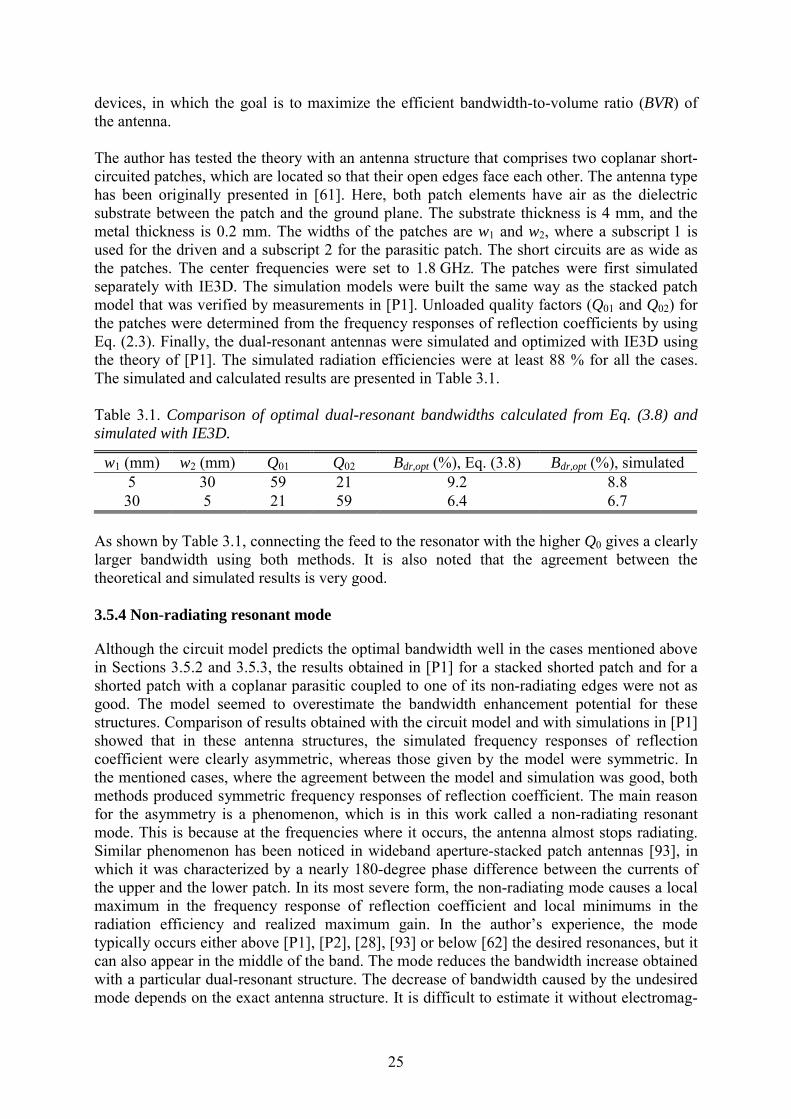
25
devices, in which the goal is to maximize the efficient bandwidth-to-volume ratio (BVR) of the antenna. The author has tested the theory with an antenna structure that comprises two coplanar short-circuited patches, which are located so that their open edges face each other. The antenna type has been originally presented in [61]. Here, both patch elements have air as the dielectric substrate between the patch and the ground plane. The substrate thickness is 4 mm, and the metal thickness is 0.2 mm. The widths of the patches are w1 and w2, where a subscript 1 is used for the driven and a subscript 2 for the parasitic patch. The short circuits are as wide as the patches. The center frequencies were set to 1.8 GHz. The patches were first simulated separately with IE3D. The simulation models were built the same way as the stacked patch model that was verified by measurements in [P1]. Unloaded quality factors (Q01 and Q02) for the patches were determined from the frequency responses of reflection coefficients by using Eq. (2.3). Finally, the dual-resonant antennas were simulated and optimized with IE3D using the theory of [P1]. The simulated radiation efficiencies were at least 88 % for all the cases. The simulated and calculated results are presented in Table 3.1. Table 3.1. Comparison of optimal dual-resonant bandwidths calculated from Eq. (3.8) and simulated with IE3D.
w1 (mm) w2 (mm) Q01 Q02 Bdr,opt (%), Eq. (3.8) Bdr,opt (%), simulated 5 30 59 21 9.2 8.8 30 5 21 59 6.4 6.7
As shown by Table 3.1, connecting the feed to the resonator with the higher Q0 gives a clearly larger bandwidth using both methods. It is also noted that the agreement between the theoretical and simulated results is very good. 3.5.4 Non-radiating resonant mode
Although the circuit model predicts the optimal bandwidth well in the cases mentioned above in Sections 3.5.2 and 3.5.3, the results obtained in [P1] for a stacked shorted patch and for a shorted patch with a coplanar parasitic coupled to one of its non-radiating edges were not as good. The model seemed to overestimate the bandwidth enhancement potential for these structures. Comparison of results obtained with the circuit model and with simulations in [P1] showed that in these antenna structures, the simulated frequency responses of reflection coefficient were clearly asymmetric, whereas those given by the model were symmetric. In the mentioned cases, where the agreement between the model and simulation was good, both methods produced symmetric frequency responses of reflection coefficient. The main reason for the asymmetry is a phenomenon, which is in this work called a non-radiating resonant mode. This is because at the frequencies where it occurs, the antenna almost stops radiating. Similar phenomenon has been noticed in wideband aperture-stacked patch antennas [93], in which it was characterized by a nearly 180-degree phase difference between the currents of the upper and the lower patch. In its most severe form, the non-radiating mode causes a local maximum in the frequency response of reflection coefficient and local minimums in the radiation efficiency and realized maximum gain. In the author’s experience, the mode typically occurs either above [P1], [P2], [28], [93] or below [62] the desired resonances, but it can also appear in the middle of the band. The mode reduces the bandwidth increase obtained with a particular dual-resonant structure. The decrease of bandwidth caused by the undesired mode depends on the exact antenna structure. It is difficult to estimate it without electromag-

26
netic simulations. The results of [P1] show that the resonant frequency of the mode can be affected with antenna design. The bandwidth and efficiency of many antenna structures could be improved if the non-radiating mode could be moved outside the desired band without affecting the desired resonances. However, finding such methods requires further research.

27
4 Effect of terminal chassis on the performance of mobile phone antennas
4.1 GENERAL
Most of the antennas used in current mobile phones are small unbalanced antennas for which the existence of a ground plane or a counterweight is essential. This group includes e.g. short whips, normal mode helices, IFAs (inverted-F antennas), PIFAs (planar inverted-F antennas), shorted patches, and their derivatives. When attached to a fairly small finite ground plane, various characteristics of these antennas are typically very different from those of the same antennas on a large or infinite ground plane. In mobile phones, the metal chassis of the termi-nal acts as a finite ground plane or counterweight for the antenna. In today’s typical mobile phone, the metal chassis mainly consists of the ground conductors of the phone’s multilayer printed wiring board (PWB), the metal covers of the electromagnetic-interference (EMI) shields [94], and other metal components that are connected to the ground conductors of the PWB. Together these parts typically form a few millimeters thick metal structure, which has the length and width approximately equal to those of the PWB. From the RF currents point of view, the basic metal chassis is essentially solid, and it can be approxi-mated as a fairly thin metal plate. A long time ago [95], [96], it was shown that the efficiency of an electrically small antenna can be increased considerably by using it to excite currents on a larger metal object, which is a more efficient radiator because of its electrically larger size. In more recent publications, motivated by the rapid growth of mobile communications, it has been shown that various characteristics, like the impedance bandwidth [6], [12], [P5], [P6], radiation efficiency in talk position [97], [P6] radiation pattern shape [27], [98], and SAR [27], [97], [99], [P6] of mobile phone antennas depend strongly on the size of the metal chassis as well as on the position and orientation of the antenna on it. Based on the results of [95] and [96], it is already clear that both the antenna element and the finite metal object, onto which the antenna is attached, form a radiating system or an antenna system, in which both components are equally important for the performance. Therefore, to optimize the performance both of these should be considered in the design. This applies also to reporting scientific research results. As the effect of chassis is so strong, the chassis dimensions and antenna location should be reported in addition to the antenna design parameters, otherwise objective comparison of antenna performances becomes impossible. For a more complete picture on the performance of e.g. a mobile phone antenna, the user should also be included in the antenna system. This thesis presents a novel approach for analyzing the combined performance of the antenna and the chassis of a mobile phone [P5]. The main idea is to consider the antenna and the chassis as a system of coupled radiating resonators. The resonator-based analysis is described briefly in the next section. Ideas that emerged during the study reported in [P5] have been studied further in [P6], in which the effect of the chassis on the bandwidth, efficiency, and SAR of internal mobile phone antennas is studied with electromagnetic simulations. The rest of the chapter discusses the main findings of this work [P5], [P6], along with those presented in the open literature, on the effect of the chassis on the performance of internal mobile phone antennas.

28
4.2 RESONATOR-BASED ANALYSIS
A mobile phone antenna is typically self-resonant and has a characteristic resonant wavemode with fields and currents concentrated near the antenna element. For this wavemode, the metal chassis of the phone acts as a ground plane creating the mirror-image effect for the antenna element. The chassis length is typically slightly less than λ0/2 at 900 MHz and between λ0/2 and λ0 at 1800 MHz, whereas the width and thickness are clearly smaller. Thus, the chassis can also support resonant modes of its own with longitudinally dipole-like current distributions, which are clearly distinct from those of the antenna element. The resonant mode of the antenna is excited by its feed. The antenna in turn excites the resonant modes of the chassis causing significant radiating currents to flow all over it. The level of the currents depends on the coupling between the modes of the antenna and the chassis as well as on the dimensions of the chassis. An example of a current distribution on the chassis of a mobile phone at 900 MHz is shown in Fig. 4.1, where the different distributions of the antenna and the chassis mode can be easily distinguished.
0
20
40
0
20
40
60
80
100
120
0.25
0.5
0.75
1
Width (mm)
Length (mm)
Ave
rage
cur
rent
den
sity
(A
/m)
Figure 4.1. Simulated current density distribution on the chassis of a mobile phone at 900 MHz showing the current concentration of the antenna wavemode and the dipole-like sinusoidal current distribution and edge maxima of the chassis wavemode. The phone contains an internal shorted patch antenna [P5]. Formally, the above-described system of coupled resonators can be represented with an equivalent circuit. A single-resonant single-band antenna attached to a typical mobile phone size chassis can be studied with a circuit model that comprises two coupled resonant circuits. For example, in the case of probe-fed shorted patch type internal antennas (Figs. 4.2a and 4.2b), the resonant mode of the antenna can be represented by a parallel resonant circuit and the resonant mode of the chassis by a series resonant circuit (Fig. 4.2c). The resonant circuits are coupled by an ideal transformer. Furthermore, an additional ideal transformer can be used to describe the coupling of the feed to the antenna-chassis combination.
Resonant mode of chassis
Resonant mode of antenna
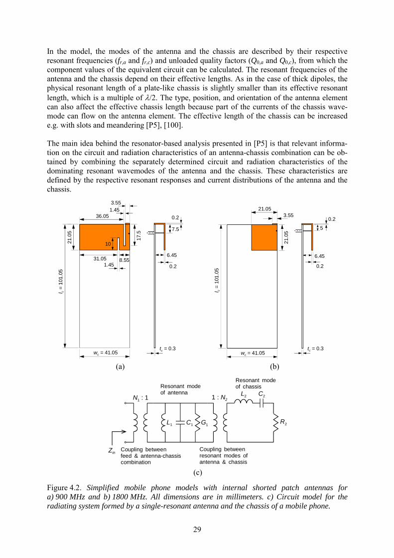
29
In the model, the modes of the antenna and the chassis are described by their respective resonant frequencies (fr,a and fr,c) and unloaded quality factors (Q0,a and Q0,c), from which the component values of the equivalent circuit can be calculated. The resonant frequencies of the antenna and the chassis depend on their effective lengths. As in the case of thick dipoles, the physical resonant length of a plate-like chassis is slightly smaller than its effective resonant length, which is a multiple of λ/2. The type, position, and orientation of the antenna element can also affect the effective chassis length because part of the currents of the chassis wave-mode can flow on the antenna element. The effective length of the chassis can be increased e.g. with slots and meandering [P5], [100]. The main idea behind the resonator-based analysis presented in [P5] is that relevant informa-tion on the circuit and radiation characteristics of an antenna-chassis combination can be ob-tained by combining the separately determined circuit and radiation characteristics of the dominating resonant wavemodes of the antenna and the chassis. These characteristics are defined by the respective resonant responses and current distributions of the antenna and the chassis.
wc = 41.05
l c =
101.
05
21.0
5 7.5
1.458.5531.05
36.05 0.2
6.45
0.2
17.5
10
1.453.55
tc = 0.3
wc = 41.05
21.0
5
l c =
101.
0521.05
5
6.45
3.55
tc = 0.3
0.2
0.2
(a) (b)
L1 C1 G1
N1 : 1 1 : N2
R2
C2L2
Zin
Resonant mode of antenna
Resonant modeof chassis
Coupling betweenfeed & antenna-chassiscombination
Coupling betweenresonant modes ofantenna & chassis
(c) Figure 4.2. Simplified mobile phone models with internal shorted patch antennas for a) 900 MHz and b) 1800 MHz. All dimensions are in millimeters. c) Circuit model for the radiating system formed by a single-resonant antenna and the chassis of a mobile phone.
30
Typically, the resonant mode of the chassis has a considerable effect on the characteristics of an antenna-chassis combination. This makes it difficult to determine a separate unloaded quality factor for the antenna mode (Q0,a). Although there are other methods, as explained in [P5], representative values showing the difference in Q0,a at different frequency ranges can be obtained by studying the ultimate lower limit for the radiation quality factor of a small antenna (Eq. 2.4) [10], [11], [33], [34]. A typical internal mobile phone antenna and the major parts of its wavemode can be enclosed in a sphere having a radius of 15 mm. In this case, the minimum radiation quality factor for a single-mode antenna is around 50 at 900 MHz and around 7 at 1800 MHz. For practical antenna elements, the radiation quality factor is known to be several times higher. By taking into account the internal loss of the antenna element, practical minimum values of Q0,a ≈ 100 at 900 MHz and Q0,a ≈ 15 at 1800 MHz were estimated in [P5]. As in the case of dipole antennas, the unloaded quality factor of the chassis (Q0,c) depends mainly on its transversal dimensions (or thickness). According to results obtained with a well-known commercial method-of-moments based simulator (IE3D), the unloaded quality factor of the λ/2-resonance of a thin, 40 mm-wide metal plate in free space is around 3 at 900 MHz, whereas the unloaded quality factor of the λ-resonance of the same plate is approximately 4 at somewhat above 1800 MHz [P5]. In the model, the coupling of the feed to the antenna-chassis combination is described with the coupling factor N1, whereas the coupling between the resonant modes of the antenna and the chassis is described with N2. The values of both coupling factors increase as the respective couplings increase. For example, in the case of a probe-fed patch type antenna, N1 increases as the probe is moved towards the electric field maximum of the patch. The value of N2 depends at least on the type and size of the antenna as well as its location on the chassis. Antennas located near the ends of the chassis are mainly capacitively coupled through their electric fields. Inductive coupling near the magnetic field maximums is also possible with loop-like antenna structures. As discussed above, Q0,a in modern mobile phones is typically much larger than Q0,c. Usually, the antenna elements are electrically so small that the bandwidth of the antenna mode alone is not sufficient for most communication systems. Thus, some help is needed from the chassis mode, the bandwidth of which is more than sufficient for most communication systems. The effect of the chassis on various characteristics of an antenna-chassis combination depends mainly on the coupling between the resonant modes of the antenna and the chassis. The bandwidth of the antenna mode determines how strongly it must be coupled to the chassis mode in order to obtain the desired bandwidth. This defines the relative excitation of the antenna and chassis modes (the level of chassis currents), which in turn determines how strongly the chassis dimensions affect various characteristics of the antenna-chassis combination, such as bandwidth, far-field radiation pattern, efficiency, and SAR. The smaller the antenna mode bandwidth, the more strongly it must be coupled to the chassis for a given bandwidth, and the more the chassis dimensions affect the mentioned characteristics. For a given coupling between the antenna and the chassis modes, their relative amplitudes de-pend also strongly on the ratio of the resonant frequencies of the modes. The maximum am-plitude of the chassis mode occurs when its resonant frequency matches that of the antenna. This maximizes the impedance bandwidth of the combination of antenna and chassis. The more fr,c and fr,a differ from each other, the stronger coupling is needed for a given bandwidth.

31
The resonator-based analysis makes it possible to study also the connection between the impedance characteristics and the relative contributions of the antenna and the chassis modes to the total radiated power. When the impedance bandwidth is around 10 % (Lretn ≥ 6 dB), it is estimated for a typical mobile phone in [P5] that the antenna mode contributes only about 10 % of the total radiated power at 900 MHz. At 1800 MHz, the contributions of the antenna and the chassis modes are of the same order. Thus, the contribution of the antenna mode at 1800 MHz is clearly more significant than at 900 MHz.
4.3 BANDWIDTH
4.3.1 Effect of chassis dimensions
Length The effect of the chassis length on the free space impedance bandwidths of 900 MHz PIFAs mounted on relatively large portable radios was studied first in [12] and soon after that in [101]. It was experimentally shown in [12] that the impedance bandwidth reaches its maximum value at a certain chassis length, which depends on the antenna configuration. For a single PIFA, the maximum bandwidth is obtained at a chassis length of about 0.4λ0. The authors of [12] concluded that more research is needed to clarify the reason for the discovered bandwidth behavior. More recently, the effect of the chassis length on the bandwidth of shorted patch type internal antennas has been studied for more compact devices with dimensions closer to those of modern mobile phones in this work [P5], [P6] and in [27], [28], [102]-[107]. These publications complement the work of [12] and [101] providing a more complete picture of the interaction of a small antenna and a chassis. It is shown in this work [P5], [P6], [102], [103] that the smallest bandwidth is obtained in free space when the chassis size equals that of the antenna. The bandwidth increases as the chassis length is increased until the first maximum is reached at a length of around 0.4λ0. Another maximum occurs when the chassis length is increased from 0.4λ0 by 0.5λ0, which was missed in the studies that considered only 900 MHz antennas [12], [27], [101], [104]. Significant progress in understanding the effect of the chassis on the performance of mobile phone antennas has been made in this work [P5]. The combination of a small antenna and a chassis is considered as a system of coupled resonators, the performance of which is mainly defined by the interaction of the dominating resonant modes of the antenna and the chassis [P5]. The theoretical results show that if the resonant modes of the antenna and the chassis are coupled, the bandwidth of the antenna-chassis combination increases considerably when the resonant frequency of the chassis mode, which is mainly controlled by the physical length of the chassis, approaches the resonant frequency of the antenna mode. The maximum band-width is obtained when the resonant frequency of a chassis mode equals that of the antenna mode. The length of current mobile phones is usually clearly larger than the other dimensions. Therefore, a typical phone chassis supports longitudinally dipole-like current distributions, and a chassis resonance occurs when the effective length of the chassis is a multiple of λ/2 at the desired frequency. The physical length is usually slightly shorter than the effective one, which depends on the chassis shape and in practice also on the antenna configuration. The results of this work [P5] explain the dependency of bandwidth on the chassis length noticed e.g. in [12].

32
In [27], it was shown that also the impedance bandwidth of a normal-mode helix antenna depends strongly on the chassis length. Within the studied range of chassis lengths (0.12λ0…0.36λ0 at 900 MHz), the general bandwidth behavior of a normal-mode helix as a function of the chassis length is very similar to that of a PIFA, which supports the claim of [P5] that the resonator-based analysis can also be used for other small handset antenna types than shorted patches. Width The impedance bandwidth of a shorted patch type antenna depends also on the width of the chassis [27], [101], [107]-[109]. As can be expected, the chassis resonates also when its effective width is a multiple of λ/2. If the resonant frequency matches that of the antenna, the bandwidth increases strongly, unless the chassis is already longitudinally resonant [106], [108], [109]. The results of [101], [106], [108] show that making the chassis narrower than the patch, so that the patch extends partly outside the edge of the chassis, increases the bandwidth of shorted patch type antennas. This increases the coupling between the resonant modes of the antenna and the chassis the same way as extending the antenna longitudinally outside the chassis [P5]. On the other hand, when the chassis is made wider than the antenna element, the bandwidth decreases, especially if the chassis is near longitudinal resonance. The bandwidth begins to increase again when the chassis width approaches the next resonant width [109]. Thickness
The effect of the chassis thickness on the impedance bandwidth of shorted patch type antennas has been studied in [101] for relatively large phones with thick chassis (0.19λ0…0.31λ0 at 940 MHz) and more recently in [108] using smaller chassis thicknesses (0.003λ0…0.06λ0 at 900 MHz and 0.007λ0…0.13λ0 at 1800 MHz). Within the studied range of values, the thickness of the chassis had only a minor effect on the bandwidth of antennas positioned completely on top of the chassis. 4.3.2 Effect of antenna location and orientation
It is mentioned in [12] that the bandwidth of internal PIFAs depends on the location of the antenna on the chassis. The general dependency of bandwidth on the antenna location can also be explained using the resonator-based analysis [P5]. As mentioned in Section 4.2, the band-width depends on the coupling between the resonant modes of the antenna and the chassis as well as on the unloaded quality factors of the modes. The maximum bandwidth is obtained at a location and with an orientation that maximize the coupling between the antenna and the chassis modes. The chassis can be viewed as a resonator formed by a single conductor transmission line bounded by two impedance discontinuities (open ends). It supports dipole-like resonant modes, and e.g. an effectively λ/2-long chassis has its electric field maximums at the open ends of the chassis and a magnetic field maximum at the center of the chassis like a half-wave dipole. Shorted patch type antenna elements couple mainly capacitively. For maximal bandwidth, such antennas should be located at the electric field maximums of the chassis. Inductively coupled antennas, such as small loops, should be located at the magnetic field maximums near the center of the chassis. For maximal coupling, the relevant fields of the antenna and the chassis modes should be oriented in parallel.

33
The results of this work [P5] and [110] show that the orientation of a shorted patch type internal antenna element on a chassis has a considerable effect on the impedance bandwidth. Generally, the largest bandwidth is obtained when the short circuit is positioned at the shorter edge of the chassis as in Fig. 4.2. Furthermore, the results of [110] indicate that placing a relatively narrow shorted patch, which has a short circuit at the shorter edge of the chassis, at one of the longer edges of the chassis rather than between them will provide a larger band-width. For example, moving a 5 mm-wide shorted patch from the center to the edge increased the bandwidth by a factor of over 2.5 at 1800 MHz. Increasing the patch width reduces the improvement factor. Recently, it has been systematically shown that the best bandwidths for antennas like shorted patches, which couple capacitively to the resonant mode of the chassis, are obtained by placing the antennas at the edges of the top (or bottom) part of the chassis [111]. As shown in this work [P5], locating a shorted patch type of antenna so that its open-end is partly outside the chassis increases the coupling between the antenna and the chassis modes and thus also the bandwidth. Examples of antennas that utilize this technique are presented in [112], [157]. 4.3.3 Effect of head and hand
In typical talk position, the resonant modes of the antenna and the chassis are loaded by human tissue, which from the electromagnetic point of view represents lossy dielectric material. In theory [31], loading a resonator with lossy dielectric material decreases its resonant frequency and unloaded quality factor. Both quantities decrease the more, the larger portion of the space containing the electric field of the resonator is filled with the dielectric. In addition, the resonant frequency decreases the more, the higher the electric field intensity is in the parts containing the dielectric, and the larger is the relative permittivity of the dielectric. Increasing the loss tangent of the dielectric decreases the unloaded quality factor [31]. It is known that placing a finger (or hand) on top of a patch antenna decreases its resonant frequency and degrades the impedance match [8]. The changes are larger if the finger is placed at the radiating edge, where the electric field intensity is the strongest, than if the finger is placed at the short-circuited edge [113]. According to [106], placing a phone model in typical talk position beside a head (without hand) caused only small changes in the behavior of impedance bandwidth as a function of chassis length compared to the behavior in free space. The distance between the head and the chassis was 7 mm, which is a typical distance used in current mobile phones. 4.3.4 Effect of chassis on input impedance level
Changing the chassis length affects the impedance level at the feed point of e.g. a shorted patch antenna. An example of this is shown in Fig. 4.3, which presents the simulated input impedance loci for the phone models of Fig. 4.2 at several chassis lengths (lc). The sizes of the loops decrease when the bandwidth (potential) of the antenna-chassis combination increases, which is here due to increased radiation by the chassis. The changes are larger at 900 MHz than at 1800 MHz, because the relative radiation contribution of the chassis is larger, as explained in [P5].

34
Owing to the changing impedance level, e.g. a shorted patch antenna must be re-matched for mobile phones of different lengths. The dependency of impedance level on the phone length can complicate antenna design for phones, in which the length of the chassis changes in different use positions such as clamshell (or fold) phones and other extendable phones. Furthermore, the changing impedance level can complicate the design of frequency-tunable antennas because the electrical length of the chassis changes along with the resonant frequency. The impedance level may have to be transformed together with tuning the resonant frequency.
lc = 0.12λ
0lc = 0.18λ
0lc = 0.25λ
0lc = 0.31λ
0lc = 0.38λ
0lc = 0.45λ
0lc = 0.51λ
0lc = 0.57λ
0
Start0.7 GHz
Stop1.2 GHz
lc = 0.25λ
0lc = 0.36λ
0lc = 0.48λ
0lc = 0.60λ
0lc = 0.73λ
0lc = 0.85λ
0lc = 0.96λ
0lc = 1.08λ
0
Start1.4 GHz
Stop 2.2 GHz
(a) (b) Figure 4.3. Simulated input impedances at several chassis lengths (lc) for the a) 900 MHz and b) 1800 MHz antenna models of Fig. 4.2. Electrical chassis lengths were calculated at the frequencies of minimum reflection coefficients.
4.4 RADIATION EFFICIENCY AND SAR IN TALK POSITION
When a mobile phone is beside a user’s head, the radiation efficiency and SAR values depend considerably on the length, width, thickness, and shape of the phone chassis as well as on the distance between the head and the chassis. The hand of a user has also an effect on the radiation efficiency and SAR results. The effect of a hand depends on its size and the way the phone is held (or the hand model). In the following, the effects of various chassis related parameters on the radiation efficiency and SAR are briefly discussed. The topic is discussed more thoroughly in [106], which is an extension of the study started in this work [P6]. 4.4.1 Effect of chassis dimensions
Length
The effect of the chassis length on the radiation efficiency and SAR of mobile phones containing shorted patch type internal antennas has been studied with finite-difference time-domain (FDTD) simulations in [97] and in this work [P6]. The results of [97] show that the smallest efficiencies occur nearly at the same chassis lengths at which the SAR values, averaged over 1 g and 10 g of tissue, reach their maximums. Based on the data presented in [97], it can be calculated that the smallest efficiencies occur at the electrical chassis lengths from 0.33λ0 to 0.38λ0, whereas the largest SAR values occur at the chassis lengths from 0.37λ0 to 0.42λ0, depending on the case. It is also concluded in [97] that the SAR values are reduced up to 30 % from the maximum ones for the chassis lengths of about λ0/4 and λ0/2.

35
However, it is not considered in [97] how changing the chassis length affects the bandwidth. Furthermore, no explanation is offered for the discovered behavior. In this work [P6], the effect of the chassis length on the radiation efficiency and SAR has been studied together with the impedance bandwidth. The results show that the maximum impedance bandwidth in free space occurs at a chassis length of about 0.38λ0 both at 900 MHz and at 1800 MHz because at that length the longitudinal resonant frequency of the chassis matches that of the antenna, as reported in [P5]. The results of [P6] also show that the radiation efficiency decreases and the SAR values increase compared to the general trends at a chassis length of around 0.36λ0 both at 900 MHz and at 1800 MHz (Fig. 4.4). This is nearly the same chassis length that gives the maximum impedance bandwidth in free space. The discovered behavior suggests a connection between the bandwidth, efficiency, and SAR in typical talk position. The radiation efficiency decreases and the SAR values increase, when the bandwidth increases due to increased chassis radiation, which in this case is caused by a chassis resonance. The results of [P6] also show that the behavior of SAR as a function of chassis length depends on the distance of the chassis from the head (Fig. 4.4). Despite the differences in the antenna and phone models as well as in the positioning of the phone beside the head, the results of this work agree qualitatively with those of [97]. The chassis resonance and the results of this work [P5], [P6] explain also the behavior found in [97].
20 40 60 80 100 120 140 160 180 2000
5
10
15
20
25
30
35
40
Length of chassis (mm)
SA
R (
W/k
g)
0.06 0.12 0.18 0.24 0.3 0.36 0.42 0.48 0.54 0.6
−6
−5.5
−5
−4.5
−4
−3.5
−3
−2.5
−2
Length of chassis (λ0)
Effi
cien
cy (
dB)
20 40 60 80 100 120 140 160 180 2000
5
10
15
20
25
30
35
40
Length of chassis (mm)
SA
R (
W/k
g)
0.12 0.24 0.36 0.48 0.6 0.72 0.84 0.96 1.08 1.2
−6
−5.5
−5
−4.5
−4
−3.5
−3
−2.5
−2
Length of chassis (λ0)
Effi
cien
cy (
dB)
Max. SAR, d = 7 mmMax. 1g avg. SAR, d = 7 mmMax. 10g avg. SAR, d = 7 mmEfficiency, d = 7 mmMax. SAR, d = 2 mmMax 1g avg. SAR, d = 2 mmMax. 10g avg. SAR, d = 2 mmEfficiency, d = 2 mm
Max. SAR, d = 7 mmMax. 1g avg. SAR, d = 7 mmMax. 10g avg. SAR, d = 7 mmEfficiency, d = 7 mmMax. SAR, d = 2 mmMax 1g avg. SAR, d = 2 mmMax. 10g avg. SAR, d = 2 mmEfficiency, d = 2 mm
(a) (b)
Figure 4.4. Effect of chassis length on SAR values and radiation efficiencies of a mobile phone positioned beside an anatomical head model at a) 900 MHz and b) 1800 MHz. Hand is not included in the model. Solid lines represent cases in which distance from head to phone d ≈ 7 mm. Dashed lines represent cases in which d ≈ 2 mm. Pin = 1 W [P6]. The effect of the chassis length on the bandwidth and SAR of shorted patch type internal antennas has also been studied in [27], [99]. The radiation efficiency is not considered in these papers. Generally, the SAR results of both [27] and [99] are inconsistent with the results of this work [P6] and [97]. This is mainly due to differences in the head models. A spherical homogeneous head model is used in [27], whereas a flat homogeneous head model is used in

36
[99]. In this work [P6] as well as in [97], a heterogeneous model of human head and shoulders, which consists of six different tissue types, is used. According to [106], simulations with the Specific Anthropomorphic Mannequin (SAM) head model, which is the standardized head model used for SAR evaluations [18], [19], give similar results as those presented in this work [P6]. The effect of the chassis on other antenna types used in mobile phones than shorted patches (or PIFAs) has also been studied. The effect of chassis length on the radiation efficiency and SAR of quarter-wave whips attached to fairly large portable radios is studied in [97]. The effect of chassis length, width, and antenna location on the impedance bandwidth, radiation pattern, and SAR of a 900 MHz helix has been considered in [27]. Width The SAR values and the radiation efficiency in talk position depend also on the width of the chassis [106], [108]. A chassis begins to resonate when its effective width approaches a multiple of λ/2. Generally, SAR values increase and radiation efficiency in talk position decreases, when the bandwidth increases due to an increased contribution of the chassis mode, which can happen either because the chassis becomes resonant or because of increased coupling between the antenna and the chassis modes. The effect of a transversal resonance is more pronounced when the chassis is longitudinally non-resonant. As mentioned in Section 4.3, the bandwidth of a shorted patch antenna increases because of increased coupling between the antenna mode and the chassis mode when the chassis is made narrower than the patch so that the patch extends partly outside the chassis [106], [108]. This increases SAR values and reduces radiation efficiency. The boundary for this effect is not abrupt. The SAR values begin to increase and the efficiency begins to decrease gradually already when the chassis width approaches that of the antenna. Thickness
Increasing the chassis thickness so that the distance from the chassis to a head remains constant but the antenna element moves farther away decreases SAR values and increases radiation efficiency. The effect is similar to moving a combination of an antenna and a thin chassis away from the head [106], [108].
4.4.2 Effect of distance from phone to head
Generally, the SAR values decrease and the radiation efficiency increases as the distance between lossy tissue and a mobile terminal increases [8], [105], [106]. However, the results of this thesis [P6] provide novel information by showing that when a combination of an internal antenna and a chassis is positioned close to the head of a user, the rate at which the SAR values change with distance depends on the dimensions of the chassis (see Fig. 4.4). When the chassis is non-resonant, the SAR values decrease monotonously as the terminal is moved away from the head [106]. With a resonant or nearly resonant chassis, the SAR values decrease slower with increasing distance than with a non-resonant chassis. When the chassis is resonant, the SAR values can even increase with increasing distance if the terminal is fairly close to the head (Fig. 4.4). The radiation efficiency increases with increasing distance from the head. When the chassis is resonant, the efficiency is generally lower than when the chassis is non-resonant.

37
4.4.3 Effect of antenna location and orientation
Internal shorted patch type mobile phone antennas are typically located on the backside and near the top of the phone. One reason for this is that for patch type antennas the necessary coupling to the chassis mode, which is required for the desired bandwidth, is easiest to obtain at the top and bottom ends of the chassis. The antennas are located on the backside of the phone because this is considered to lead to the lowest SAR values and the highest radiation efficiency. Near the top of the phone, the antenna is less likely to be disturbed by a user’s hand. When the bandwidth of a single-resonant small internal antenna in a mobile phone is roughly 10 % at 900 MHz, the radiation contribution of the antenna mode is so small that significant SAR reduction in the head or radiation efficiency improvement in talk position cannot be achieved by redesigning the antenna element or by changing its orientation on the chassis [P5]. The reduction of SAR requires decoupling of the antenna mode from the chassis mode, which will reduce the bandwidth. This could be done e.g. by moving the antenna closer to the longitudinal center of the chassis. Owing to the dominant role of the chassis mode, at 900 MHz, efficiency improvements in talk position and SAR control should be attempted by changing the distribution of the chassis currents using methods presented in [115] and [116]. At 1800 MHz and above, where the contribution of the antenna mode is more significant, it is possible to reduce the SAR values and to increase the radiation efficiency by locating a shorted patch antenna correctly. When the antenna element is located on the backside of the chassis, the most of the radiated field is directed away from the head, which reduces SAR and increases radiation efficiency. The results of [105], [106] show that at 1800 MHz and above, the SAR values and the radiation efficiency depend on the antenna orientation (location of feed and short circuit). 4.4.4 Effect of hand
Generally, the effect of a user’s hand on the SAR values and radiation efficiency depends on the frequency, chassis dimensions, hand size, and the way the phone is held (hand model and its position on chassis) [108]. Including a hand in the evaluation reduces SAR values in the head because the hand absorbs some of the power [114]. However, the general behaviors of SAR values in the head and radiation efficiency as functions of various chassis related parameters have been noticed to be similar with and without the hand [106], [108]. A hand can reduce the radiation efficiency of an antenna-chassis combination considerably. Based on the results of [108], it can be estimated that a hand can cause additional radiation efficiency reductions ranging from 2 to 6 dB at 900 MHz and from 1 to 7 dB at 1800 MHz depending on the hand model and its location. The largest radiation efficiency reductions occur when the hand covers those parts of the phone that are the main contributors to the radiated power [106], [108].

38
5 Design of multiband internal antennas for handsets
5.1 GENERAL
Current wireless communication systems utilize several different radio communication standards and operate at many different parts of the frequency spectrum. In this fractured service environment, terminals operating in multiple systems and frequency bands can offer a better service coverage than single-band and single-system terminals. Multiband antennas are essential components of multiband terminals. Generally, there seems to be an increasing trend in the number of radios in a mobile terminal, which translates into an increase in the number of antennas or antenna functions. For example, a basic European mobile phone uses the Global System for Mobile Communications (GSM) standard and operates at the 900 and 1800 MHz frequency bands. Globally, GSM networks are currently used also at 850 and 1900 MHz frequency bands, and many recent GSM phones operate already at three frequency bands (GSM900/1800/1900). The next logical step is a quad-band (GSM850/900/1800/1900) terminal. The commercial use of Universal Mobile Telecommunication System (UMTS) networks utilizing Wideband Code Division Multiple Access (WCDMA) technology has also been started, and new networks are gradually being opened to the general public. The first published UMTS terminals intended for European markets are multiband and multimode GSM/UMTS devices. In addition to cellular systems, mobile phones have radios that utilize non-cellular wireless communication standards, such as Bluetooth (BT) short range radio link and Global Positioning System (GPS). Many recent phones have also an analog FM radio receiver. Some manufacturers have announced plans to incorporate Digital Video Broadcasting for Handheld (DVB-H) receiver and Wireless Local Area Network (WLAN) functions into their terminals. Future mobile terminals may also utilize Radio Frequency Identification (RFID) and Ultra Wideband (UWB) systems. When this thesis work began in 1997, commercial mobile phones were single-band single-system terminals with external whip or helix antennas. In the field of multiband antennas, the thesis has mainly concentrated on the development of internal multiband antennas for cellular systems, such as GSM and UMTS. The antennas are mainly based on shorted patch (or PIFA) type of antenna elements, which are demonstrated on monoblock type of phones. However, the studied techniques can also be applied to antennas designed for other systems and terminal types. A considerable number of antennas for mobile phones have been published recently, enough to be organized into a book [117]. In the following, a short overview of existing shorted patch (or PIFA) type internal multiband antennas and their design techniques is presented to illustrate the recent progress in the field. The author’s contributions are included in the overview. The main contributions of this work are also summarized in Sections 5.3 and 5.4.
5.2 GENERAL REALIZATION METHODS
5.2.1 Separate antenna elements
Irrespective of the antenna type, a multiband antenna can be constructed by combining two or more separate single-band antenna elements. If a large isolation can be achieved between the antenna elements operating at different bands, they can be optimized nearly independently,

39
which simplifies the design. For example, a matching circuit or a parasitic element can be easily added to each antenna element to increase their bandwidth. Figure 5.1a shows an example of a dual-band PIFA realized with two separate closely-spaced antenna elements [118]. The isolation between the 900 and 1800 MHz antenna elements is at least 17 dB despite a small distance of 2 mm between the elements. A related design for 900 and 1800 MHz that consists of two separate closely-spaced capacitively-loaded PIFAs with capacitive feeds is presented in [119]. The structure of [118] has later been modified by adding a third PIFA to create a triple-band antenna with resonances at 900, 1890, and 2440 MHz [120], [121]. 5.2.2 Single element having two or more resonances
Antennas with one resonance per band
Another basic solution is the use of a single feed to excite two or more separate resonant frequencies in one antenna structure. There are several different ways of realizing single-feed multiband antennas. Multiband operation can be achieved by providing separate resonant current paths, but it is also possible to use the dominant and higher-order mode resonances of a single current path. Although this antenna type can be considered structurally simpler than one comprising separately fed elements, its design is more complicated. The feed must be appropriately coupled (matched) to all desired resonances, and finding a suitable coupling can be challenging. A single-feed multiband antenna can be more compact than one realized with separate elements, because at least some (and at best all) sections of the lowest band antenna element are reused for more than one resonance. Figure 5.1b shows an example of a single-feed dual-band PIFA for 900 and 1800 MHz [118], which is realized by galvanically connecting two patches near the short circuit. This provides two resonant quarter-wave current paths of different lengths and different resonant frequencies. A suitable position for the feed can be found so that both resonances are well matched. The structures can be described also so that two subpatches, sharing a short circuit and a feed, are formed by cutting an L-shaped slot to the patch. Later, various other slot shapes and patch configurations have been reported e.g. in [122], [P7].
Short circuit Feed
(a) (b) Figure 5.1. Top views of dual-band PIFAs reported in [118], a) dual-feed antenna, b) single-feed antenna. Metal strips producing the higher bands of a multiband shorted patch can also be positioned inside the area of the lower band patch. In [123], a U-shaped slot in the middle of a rectangular shorted patch was used to separate a smaller shorted subpatch from the rectangular patch. The patches shared one short circuit and were excited by a single feed (Fig. 5.2a).

40
A dual-band antenna can also be realized by utilizing the first two resonances of one resonant current path. By folding or meandering a shorted patch in a suitable way, the ratio of its first two resonant frequencies can be varied so that e.g. dual-band operation at 900 and 1800 MHz is possible. This can be done by folding a suitable section of the patch near the open end upwards on top of the rest of the patch (Fig. 5.2b) [74] or downwards between the rest of the patch and the ground plane (Fig. 5.2c) [124], [125]. The same effect can also be obtained in a single layer structure by meandering the patch in an appropriate way (Fig. 5.2d) [117], [126]. These antenna types can be modified to have three separate bands by providing an additional separate resonant current path, as in [127]. In [128] and [129], dual-band shorted patches were created by adding a rectangular slot near the open edge of a shorted patch (Fig. 5.2e) to reduce the frequency ratio of the first higher order mode (TM03) and the dominant mode (TM01). The slot was nearly as wide as the patch and located parallel to its open edge. By adjusting the length and location of the slot the frequency ratio could be varied in the range from 2 to 3 [128]. By varying the width of the short circuit, the frequency ratio of the design could be further reduced and varied in the range from 1.6 to 2.2 [129]. One possibility for realizing a dual-band PIFA, e.g. for 900 and 1800 MHz is connecting two separate patch sections with a parallel LC resonator (Fig. 5.2f) [130]. At resonance, the parallel resonator acts as an open circuit (large reactance) disconnecting the two patch sections, which produces the higher resonant frequency. At frequencies below its resonance, the parallel resonator acts as an inductive load connecting the two patch sections, which produces the lower resonant frequency.
Short circuit Feed
(a) (b) (c)
Slot
L
C
(d) (e) (f) Figure 5.2. Examples of dual-band shorted patch antennas presented in a)[123], b) [74], c) [124], d) [117], e) [129], f) [130]. Antennas with multiple resonances per band
The main frequency bands used for cellular communications worldwide are concentrated at slightly below 1 GHz and at around 2 GHz. The cellular system bands are so wide and the antennas so small that it is difficult to cover more than one system band with one resonance. It was theoretically shown by Fano [21] that the bandwidth of a passive complex load, such as a small resonant antenna, can be approximately doubled with a single lossless matching

41
resonator connected between the load and its feed line. Furthermore, it has been shown in this work that the bandwidth can be approximately doubled by dividing a single-resonant shorted patch into two narrower coplanar shorted strips [P2], [P1], or by constructing a stacked shorted patch into the same volume [P3], [P1]. The system band of GSM850 (824-894 MHz) is approximately as large as that of GSM900 (880-960 MHz), and the bands are partly overlapping. Therefore, in principle, by using any one of the mentioned bandwidth enhancement methods, an antenna covering the band of GSM850 can be improved to cover the GSM900 band [88]. The same applies to the GSM1800 (1710-1880 MHz) and GSM1900 (1850-1990 MHz) bands. It has been demonstrated in [128] that by using a rectangular slot near the open end of a relatively large PIFA (Fig. 5.2e), it is possible to design a dual-band PIFA with two resonances at the upper band. It has been shown in this work [P7] that a parasitic radiating shorted patch element can be used to make the upper band of a single-feed dual-band shorted patch antenna dual-resonant and more wideband. This was demonstrated with an internal mobile phone antenna that covers the system bands of E-GSM900, GSM1800, GSM1900, and UMTS. The antenna was realized by optimally coupling the resonance of a separate coplanar parasitic shorted patch to that of the upper band section of the driven patch. The antenna feed was also appropriately coupled to both the lower band resonance and the upper band dual resonance. Furthermore, in [P7], the most important sections of the antenna were placed adjacent to the edges of the ground plane so that the resonant modes of the antenna coupled strongly to those of the ground plane in order to maximize the bandwidths at the lower and upper operation bands. Following this work [P7], various related realizations of parasitic resonators have been proposed. In [28] and [131], a dual resonance at the upper band of a dual-band shorted patch was obtained by locating the driven and the parasitic shorted patch on different sides of the lower band shorted patch element. Sufficient coupling between the driven and the parasitic resonator was achieved by connecting the patches directly to each other at the short circuit in [28] and near the short circuit in [131]. The use of a parasitic half-wave slot resonator, which is integrated to the lower band element and parasitically coupled to the upper band element of a dual-band shorted patch, has been proposed in [116]. A metal strip resonator connected directly to the feed of a dual-band PIFA and located between the PIFA and its ground plane has been presented in [132]. The additional resonator made the upper band of the antenna dual-resonant and more wideband. A capacitive plate has been connected with a narrow metal strip between the feed and the short circuit of a dual-band shorted patch antenna to create a dual-resonant upper band in [125]. In [88], an integrated matching circuit similar to that of [125] was used to extend the lower band of a dual-band PIFA to cover both the GSM850 and GSM900 bands. The next step forward is making both bands of a dual-band antenna at least dual-resonant. A relatively large antenna structure that has four resonances grouped to two separate bands is described in [133]. The antenna comprises a shorted U-shaped patch that has arms of different lengths. This is fed by another probe-fed patch element on the same layer. According to [133], the feeding patch operates at the upper band. In [134], four resonances grouped to two separate bands were obtained by adding coplanar parasitic shorted patches to both bands of a dual-band shorted patch antenna.

42
A stacked shorted patch antenna structure with four resonances grouped to two bands is also presented in [135]. The antenna is fed to the upper patch. Each patch includes a slot that modifies the current paths so that two coupled resonances can be located near each other at both bands. In [136], a dual-band antenna with two coupled resonances at the lower and three at the upper band is presented. The antenna comprises two similar meandered patch elements and a rectangular patch in the middle. All the elements share one short circuit and one feed. 5.2.3 Matching circuits
Adding a reactive multiband matching network between an antenna element and its feed line is one way of realizing internal multiband antennas. A very compact solution can be obtained by utilizing the coupling element based antennas proposed first in this work [P5], [137]. Recently, it has been shown that at least a 6-dB return loss and a good total efficiency (> 66 %, in free space) over E-GSM900 and GSM1800 bands is possible with a single coupling element having a volume of 2.4 cm3 [111]. The coupling element is located totally on a 40 mm × 100 mm × 3 mm (width × length × height) ground plane (metal chassis). When the antenna is moved partly outside the mentioned chassis, similar bandwidth and efficiency (> 63 %) performance can be obtained with an element having a volume of only 1.3 cm3. Examples of dual-band and multiband matching circuits have recently been presented in [138]. 5.2.4 Electrical frequency tuning
A multiband operation can also be realized by tuning the resonant frequency of an antenna electrically from one frequency band to another. This can be used in applications, where the mobile terminal antenna does not have to operate simultaneously at different bands, such as in GSM. The main motivation for using frequency tuning is improved antenna performance for a given antenna size. The main disadvantages are power loss in the tuning circuit, increased design and manufacturing complexity and price as well as non-linearity of the tuning circuit. Various issues related to electrical frequency tuning are described in more detail in Chapter 6.
5.3 ON THE DESIGN OF INTERNAL MULTIBAND ANTENNAS
The bandwidth and total efficiency of internal multiband antennas are limited by the total volume allowed for the antenna. The bandwidth-to-volume ratio can be increased by generating dual or multiple resonances at each band, which can be realized with various methods, as discussed in Chapter 3 and in [P1]-[P4] and [P7]. These methods should be used whenever possible. If the bandwidth becomes larger than necessary, it can be traded off for smaller size or better matching and thus larger total efficiency. When the antenna size is small enough, even the use of known multiresonant techniques will not provide sufficient operation bandwidth. As discussed in Chapter 4 and [P5], the characteristics of a small antenna attached to a fairly small radio device depend on the relative amplitudes of the resonant modes of the antenna and the metal chassis of the radio device. The relative amplitudes depend on the coupling between the resonant modes as well as on the relative resonant frequencies of the modes. These are controlled by the size, orientation, and location of the antenna element on the metal chassis

43
and the dimensions of the metal chassis. This applies also to multiband antennas. The effect of the chassis must be analyzed separately for each band. From the basic operation point of view, the excitation of resonances at desired frequencies is obviously important in the design of multiband antennas. Currently, however, the space allowed for internal handset antennas is so small that the resonant modes of the antenna elements alone cannot cover the necessary system bandwidths. This is especially true around 900 MHz and below. At 1800 MHz and above, the contribution of the antenna mode is larger, but also there the help of the chassis is needed. When the necessary resonances have been excited, in order to obtain a sufficient operation bandwidth (matching and efficiency), the main objective is to find suitable locations and orientations for the important sections of the antenna so that its resonant modes at different operation bands couple sufficiently strongly to the nearest resonant modes of the chassis. Generally, this is not explained or considered in the basic books and scientific contributions reporting differently shaped variations of e.g. single-feed multiband PIFAs for mobile terminals.
5.4 MAIN CONTRIBUTIONS OF THIS WORK
The main contributions of this work in the field of multiband antenna design are the following. General understanding of the possibilities of two coupled radiating resonators was improved [P1] and novel antenna structures were developed [P3], [P4], [P7]. It was shown that a coplanar parasitic shorted patch could be successfully used to improve the performance of a single-feed dual-band shorted patch antenna [P7]. This was demonstrated with an internal mobile phone antenna that operates in E-GSM900, GSM1800, GSM1900, and UMTS systems. To the author’s knowledge, it is the first published antenna capable of such per-formance. Furthermore, to the author’s knowledge, the antenna type is currently being used in commercial mobile phones. It was also shown that and analyzed how various characteristics of a small antenna attached to a fairly small radio device depend on the relative amplitudes of the resonant modes of the antenna and the metal chassis of the radio device [P5], [P6]. The concept of a non-radiating coupling device, which enables optimal use of the space reserved for the antenna, was proposed in [P5], [102], [137]. This has lead to the recent development of very compact multiband antenna solutions for mobile phones [111], [138].

44
6 Design of low-loss tuning circuits for electrically frequency-tunable small resonant antennas
6.1 GENERAL
The effective bandwidth of a small resonant antenna can be increased by tuning its resonant frequency from one frequency to another. A telescopic dipole is a simple example of a fre-quency tunable antenna. Its resonant frequency can be tuned mechanically by adjusting the radiator length. This thesis considers small resonant antennas that need an electrically controlled tuning circuit for achieving a change in the resonant frequency. In small portable radio equipment, the main motivation for using frequency tuning is increas-ing the effective bandwidth-to-volume ratio of the antennas. The increased bandwidth can be used as such to increase the number of antenna functions. As the bandwidth of a small an-tenna is interrelated to its size and efficiency, any extra bandwidth obtained with electrical frequency tuning can also be traded off for smaller antenna size, which saves space inside small radio equipment. Alternatively, the extra bandwidth can be traded off for better imped-ance match. The total antenna efficiency increases, if the desired band can be covered with a larger return loss. Electrical frequency tuning can also be used to compensate for the detuning caused by external disturbances, such as nearby metal or dielectric objects [139]. Electrical frequency tuning can be used in applications where the instantaneous operation bandwidth can be smaller than the total system bandwidth. In mobile communication systems, the bandwidth of one frequency channel is typically only a fraction of the total system band-width. Therefore, it is not necessary to cover the whole system band with one large passive antenna. For example in GSM systems, a smaller narrow-band antenna could be tuned be-tween the transmitting (TX) and receiving (RX) bands because the TX and RX functions are not simultaneous [140]. Another possible application is tuning an antenna that covers a whole system band from the frequency band of one communication system to that of another, as in [P9]. Adding a frequency-tuning circuit makes an antenna structure and its design more compli-cated and increases production costs. The tuning circuit is composed of lossy devices, which can strongly decrease the radiation efficiency of the antenna [141]-[143]. Typically, electrical frequency tuning is realized with switches or varactors, which are non-linear semiconductor devices that distort the output signal. Non-linearity can limit the use of frequency tuning in high power applications, such as transmitter antennas. Besides cost, power loss, and distortion, the use of electrical frequency tuning in battery-operated portable radio equipment can be limited by DC power consumption in the control circuit. From this point of view, voltage-controlled devices are preferable over current-controlled ones. The available DC control voltage may also limit the implementation possi-bilities. As presented in [P5], the impedance bandwidth of a small resonant antenna depends strongly on the ratio of the resonant frequency of the antenna to that of the chassis. Varying the antenna resonance changes this ratio, which can have a considerable effect on the input matching of the antenna, as shown in Section 4.3.4. Matching changes can limit the useful frequency-tuning range of an antenna [P9]. When one band of a multiband antenna is tuned, the tuning circuit can have an undesired effect on the other bands. This can complicate the design of such antennas and tuning circuits.
45
6.2 FREQUENCY-TUNING METHODS
The resonant frequency of a small antenna can be tuned by loading it with a suitable addi-tional reactance that cancels out an opposite antenna reactance making the input impedance of the antenna real either below or above the original resonance. Another general method of tuning the resonant frequency is altering an antenna geometry in such a way that the effective electrical length of the antenna changes. Various miniaturization methods of small antennas offer a starting point for realizing antennas in which a frequency tuning circuit is integrated to the antenna structure. This is because miniaturization methods of small antennas can be regarded as passive methods for reducing the resonant frequency of an antenna without increasing its physical size (electrical size decreases). An antenna, whose resonant frequency has been decreased by modifying the structure, can be turned into a frequency-tunable one by adding a switch or another control component to a suitable location on the antenna so that changing the state of the control component compensates for the original modification and thus increases the resonant frequency. The resonant frequency of a short-circuited patch antenna can be decreased e.g. by reducing the width of its short circuit [6] (or by reducing the number of shorting pins), by modifying the shape of the short circuit, by cutting slots into the patch, or by meandering the patch [144]. These methods are often referred to as inductive loading. They are the most effective when applied at the current maximum of the antenna. Another well-known method is to extend the length of a patch slightly and then fold the extension towards the ground plane to avoid increasing the physical length of the antenna [145]. This is usually referred to as capacitive loading. It is the most effective at the high impedance edge of a patch, where the electric field intensity is at maximum. Lumped components can also be used for inductive and capacitive loading. In principle, most of the known passive methods for tuning an antenna resonance can be exploited also when the tuning is electrically controlled. Patch antennas that can be tuned between discrete frequencies have been realized by con-necting an additional reactive component between a patch and a ground plane [143], [146] and by connecting sections of a patch to each other [147] with a switch. The switch can be a PIN-diode, a FET-switch, or in the future possibly also a MEMS-switch. The number of short circuits connecting a patch to a ground plane has also been varied with an array of switches [148]. Continuous frequency tuning can be realized by replacing a switch with a varactor, which is a voltage controlled variable capacitor [67], [141]-[143], [149]-[151]. Frequency-tunable antennas can also be realized by adding an adjustable matching circuit between an antenna element and its feed line. As long as the input impedance of a small an-tenna contains a real part, the antenna can be matched by a circuit containing e.g. reactive lumped components, sections of transmission line, or both [23]. An apparent change in the resonant frequency can be achieved by adjusting component values used to match the antenna at one frequency so that it will be matched at a different frequency. Various frequency tunable matching circuits can be designed using varactors (or switches and fixed capacitors) in addition to fixed inductors. In such circuits, the varactors can be used e.g. to compensate for the effect of inductors.

46
6.3 EFFICIENCY AND DISTORTION
The main technical challenge in the design of frequency tunable antennas for small radio equipment is achieving a sufficiently large electrically controlled frequency shift with minimal degradation of the radiation efficiency and with minimal signal distortion. Unfortunately, information on either the efficiency or distortion characteristics [139], [141], [147], [150] or both [67], [140] has often been omitted from publications. The power loss in a given load component depends on the square of the current (rms) flowing through the load and the real part of the load:
loadloadload ZIP Re2= . (6.1) The current in turn depends on the load impedance and the voltage over it. Minimizing the RF power loss in a given load component requires minimizing the current through the component. However, without any RF current through the load (open circuit), there is no frequency shift. The larger the current through a given load is, the larger the frequency shift and the losses are. Thus, there is clearly a trade-off between frequency tuning range and power loss. Minimizing the resistive part of the load by using low-loss components is also important. An optimal frequency tuning circuit provides the largest change in the load reactance compared to the power loss in the circuit. Based on this idea, a systematic study on the minimization of power loss in certain tuning circuits of small resonant antennas has been conducted in this work [P8]. Ideally, any load reactance can be realized using a section of open-circuited or short-circuited transmission line with length < λ/2. The tuning circuit selected for the study comprised two such sections connected by a PIN-diode switch (Fig. 6.1). The arrangement forms a general electrically controlled tuning circuit that enables switching between two resonant frequencies and allows e.g. changing the direction of tuning with only minor changes in the configuration. The tuning circuit is first optimized by maximizing the change of reactance relative to the power loss based on theoretical calculations. The desired frequency shift is then set by adjusting the coupling between the tuning circuit and the antenna, which also defines the final power loss in the circuit. The coupling depends on the coupling method and the impedance level of the antenna at the point where the tuning circuit is connected to it.
l1 l2
Patch
Switch Figure 6.1. A frequency-tunable short-circuited patch antenna. Two prototypes with optimized low-loss frequency-tuning circuits were presented in [P8]. The original unloaded quality factors (without the tuning circuit) were 99 for the high-Q

47
prototype (A1) and 20 for the low-Q prototype (A2). The high-Q prototype was tuned slightly over 5 % at the expense of about 20 % decrease of efficiency, whereas the low-Q prototype was tuned slightly less than 5 % at the expense of only 3 % decrease of efficiency. To demonstrate how well the tuning circuits proposed in [P8] minimize the efficiency reduction caused e.g. by lossy switches, Fig. 6.2a shows the measured radiation efficiency as a function of the series resistance (RS) of the forward-biased PIN-diode (closed switch) for the two frequency-tunable antenna prototypes presented in [P8]. Figure 6.2a suggests a linear dependency between the radiation efficiency and the series resistance. The figure also suggests that with the tested tuning circuits the radiation efficiency would not increase considerably even if RS could be reduced to zero from the value of 2.3 Ω, which was obtained with the typical forward bias current (IF) of 10 mA. By using the method proposed in [P8], the DC bias current could be systematically reduced by 50 % or even more with only minor degradation of efficiency, which is important for antennas of battery-operated devices. The resistances given in Fig. 6.2 represent typical values taken from the datasheet of the used PIN-diode [152] based on measured bias current. Figure 6.2b shows the dependency of the series resistance on the forward bias current.
IF (mA) RS (Ω) 1 13.2 2 7.7 3 5.4 4 4.3 5 3.6 10 2.3 15 1.9 20 1.5 30 1.3
0 1 2 3 4 5 6 7 8 9 10 11 12 13 14 1540
45
50
55
60
65
70
75
80
85
90
95
100
RS (Ω)
Rad
iatio
n ef
ficie
ncy
(%)
A1A2
(a) (b) Figure 6.2. a) Measured radiation efficiency for the high-Q (A1) and low-Q (A2) prototypes of [P8] as a function of the series resistance (RS) of the closed switch. The radiation efficiencies were measured with the Wheeler cap method as in [P8]. The solid and dashed lines have been fitted to the data using the least squares method. b) Typical series resistance vs. forward bias current (IF) for a single Infineon BAR64 PIN-diode [152]. In both examples of [P8], the maximum efficiency was obtained when a forward-biased PIN-diode was located near the current maximum of a short-circuited λ/4-long section of transmission line. However, the current on the line was minimized because the impedance of the line was very high at the point where it was connected to the antenna. Owing to the minimal current through the diode, both power loss and distortion were minimized. When the PIN-diode was reverse-biased (switch open), it was located at the high impedance end of a nearly λ/4-long, nearly resonant section of transmission line, which shared a short circuit with the antenna. At this location, there was a high signal voltage over the diode, which is assumed

48
to be the main reason for the fairly high distortion in this switching state. It is assumed that the distortion can be reduced by decreasing the signal voltage over the diode. This can be done by changing the length of the first transmission line section further away from resonance, which will also reduce power loss in the tuning circuit when the switch is open. However, it will increase both power loss and distortion when the PIN-diode is forward biased. Generally, there seems to be a trade-off between the achievable efficiency and distortion performance. In [142], it was mentioned based on full-wave simulations that the efficiency of a patch loaded by a variable capacitor between the patch and a ground plane increases when the capacitor is moved closer to the radiating edge of the patch, where the maximum electric field occurs. This position maximizes the frequency shift obtained with a given reactive load [141], [151], [153] and thus a smaller capacitive load is needed for a given frequency shift. Reducing the capacitance increases the load impedance, which reduces the current through the load increasing the radiation efficiency, as explained above. Connecting a load directly between the radiating edge of a patch and its ground plane as in [142] maximizes the signal voltage over the load. Therefore, it can be assumed that this location also maximizes the distortion in certain non-linear loads, such as a reverse-biased varactor and reverse-biased PIN-diode (in series with a small capacitor or large inductor). As the load is moved towards a lower impedance part of the antenna, the signal voltage over the non-linear load decreases, which should reduce the distortion. However, a larger load capacitance is now needed for a given frequency shift, which increases the current through the load and reduces the efficiency. Therefore, this solution also suggests a trade-off between distortion performance and radiation efficiency. The distortion generated by a forward-biased PIN-diode depends on the bias current. It decreases when the bias current increases. This is shown e.g. in the datasheet of the BAR64 PIN-diode [152] used in [P8]. According to [154], distortion in forward-biased PIN-diodes is caused by the modulation of the intrinsic region conductance by charge carrier injection from the applied RF signal. The reverse bias distortion characteristics of the BAR64 PIN-diode were not given in its datasheet. In the measurements for [P8], it was noticed that the reverse-biased PIN-diodes generated more distortion than the forward-biased ones. Furthermore, it was noticed that increasing the reverse bias voltage reduced distortion. The results are consistent with those reported in [155]. Contrary to ideal PIN-diodes, the boundaries between the intrinsic and the (p and n type) end regions are not exactly abrupt in real PIN-diodes, but the doping concentrations increase continuously towards those of the end regions. Because of these so-called diffusion tails, the reverse bias capacitance of a real PIN-diode decreases continuously with increasing reverse bias voltage for voltages beyond the punchthrough as the depletion region advances into the end regions and the diode performance approaches that of an ideal one [155]. According to [155], the main reason for the reverse bias distortion is the diffusion tail related capacitance variation induced by the RF signal.
6.4 EFFECTS OF ANTENNA SIZE AND QUALITY FACTORS
When the size of a small antenna is decreased, its radiation quality factor (Qr) increases. This complicates the antenna design, because the radiation efficiency of the antenna is decreased more by a given cause of power loss [see Eqs. (2.2) and (2.7)]. Decreasing the radiation loss

49
by a certain factor requires the reduction of other losses by the same factor or otherwise the radiation efficiency decreases. For antennas that can be described with a parallel resonant circuit, such as open-circuited and short-circuited patches (and PIFAs), it was shown in this work [P8] that the frequency shift caused by a given parallel-connected reactive load is inversely proportional to the unloaded quality factor (Q0) of the antenna. Thus, the narrower the antenna bandwidth is, the larger the tuning admittance must be for a given frequency shift. It was also shown that in the studied cases, the ratio of frequency shift to the associated power loss was inversely proportional to the Q0 of the antenna. In other words, wideband antennas (low Q0) can be tuned a given amount while maintaining a higher efficiency than narrowband antennas (high Q0). Alternatively, a larger tuning range can be achieved for a given efficiency. Therefore, a lot of attention has to be paid to the material and tuning component losses when a very small, high-Q antenna is tuned. The results of [P8] also suggest that that distortion in the open state of a PIN diode switch depends on the unloaded quality factor of the antenna. When the switch was open, the low-Q prototype generated less distortion (third-order input intercept point, IIP3 = 61 dBm) than the high-Q prototype (IIP3 = 46 dBm). The reason for this seems to be a lower RF voltage over the diode. Based on circuit simulations with APLAC using the model presented in [P8], it can be estimated that the RF voltage over the PIN diode switch in the low-Q prototype was less than half of that of the high-Q prototype.
6.5 RADIATION PATTERN
Adding an electrical frequency tuning circuit to a small resonant antenna can affect its radiation pattern [142]. For example, decreasing the resonant frequency of an antenna reduces its electrical size, which decreases its directivity. However, owing to their small size, the antennas studied in this thesis have inherently low directivity (2-5 dBi), and therefore, drastic changes in directivity are not expected. When the radiator shape is changed e.g. by connecting different sections of an antenna with a switch, the polarization of the antenna can change significantly, which may limit the realization possibilities, but may also be utilized e.g. in polarization diversity systems. If active components are used to control the polarization of small antennas, similar problems can be expected as in frequency-tunable antennas. 6.6 FREQUENCY-TUNABLE INTERNAL ANTENNA FOR MOBILE PHONES
After having developed understanding on how the power loss in the frequency-tuning circuits of small antennas could be minimized, the knowledge generated in this work [P8] was applied to the design of a novel internal multiband mobile phone antenna in [P9], [156]. The goal was to tune the lower band of a previously published [122] dual-band (GSM900/1800) antenna to cover also the US cellular band (824-894 MHz). The main problem in the design was the strong dependency of the input impedance of the antenna on the electrical length of the phone chassis, as could be expected based on [P5] (see also Section 4.3.4). When the resonant fre-quency of the antenna, which was well matched at 900 MHz, was tuned to the US cellular band and thus further away from the resonant frequency of the chassis, the impedance level at the feed point of the antenna increased considerably. This made the antenna too overcoupled and poorly matched at the US cellular band. Adjusting the feed location to match the antenna at the US cellular band made it too undercoupled and poorly matched at the GSM900 band. A

50
suitable solution for matching the antenna was making it dual-resonant at both bands. This could be realized by loading the antenna with a sufficiently long section of microstrip line, the length of which could be varied. The tuning line was connected to the antenna with a narrow pin at one end. The other end was open circuited. To vary the length of the line and thus the reactive loading and the frequency of optimum impedance match, the tuning circuit was im-plemented using three sections of microstrip line and a single-pole double-throw (SPDT) switch. The first microstrip line section connected the pole of the switch to the antenna, whereas the two shorter sections were connected to the throws of the switch for varying the total line length. The power loss in the switch was minimized by locating it as close to the current minimum of the loading line as possible. The switch generated very little distortion because the voltage over it was low. Adding the tuning circuit deteriorated the bandwidth and efficiency of the antenna slightly at the 1800 MHz band. However, it should be possible to recover most of the bandwidth by adjusting the location of the feed pin. It should also be pos-sible to further increase the bandwidth with a parasitic element as proposed earlier in this work [P7].

51
7 Summary of Publications
[P1] Design and bandwidth optimization of dual-resonant patch antennas
Paper [P1] presents for the first time a unified theory for the impedance bandwidth optimiza-tion of dual-resonant antennas with arbitrary unloaded quality factors (Q01 and Q02). The the-ory is formally presented using an idealized circuit model, which makes it general enough to apply to all fairly narrow-band dual-resonant antennas that can be sufficiently accurately de-scribed with simple resonant circuits. Microstrip patch antennas are used as examples because they represent a widely used modern antenna type and because of their central position in the thesis. At first, the main electrical design parameters concerning the bandwidth optimization of dual-resonant antennas are systematically analyzed. It is shown that a system of two coupled reso-nators, such as a dual-resonant antenna, has a theoretical maximum impedance bandwidth that depends only on Q01, Q02, and the matching requirement (e.g. VSWR ≤ 2). Equations for the calculation of the maximum theoretical dual-resonant impedance bandwidth are also pre-sented. By adjusting the ratio of the resonant frequencies of the resonators (fr2/fr1), the cou-pling between the resonators, and the coupling of the feed to the driven resonator, the imped-ance bandwidth of any dual-resonant antenna structure can be controlled and optimized. To support the theory, examples of various patch antenna structures are presented. The first example shows that the electrical parameters of the circuit model have real world counterparts as dimensions of a real antenna and that the model describes the main trends of the input im-pedance locus correctly. The second example shows that the equations derived for the maxi-mum theoretical dual-resonant bandwidth are very accurate when only two resonant modes are excited. The last example reveals the existence of a non-radiating resonant mode, which can reduce the bandwidth obtained with some dual-resonant antenna structures. It explains why the theoretical maximum bandwidth is not always achieved in practice. [P2] Radiation and bandwidth characteristics of two planar multistrip antennas for mobile communication systems
The second paper [P2] presents an experimental study on the radiation and bandwidth charac-teristics of two modified short-circuited microstrip patch antennas. The impedance bandwidth of the studied antennas has been enhanced by dividing one wider patch into separate narrower patches that are tuned to slightly different resonant frequencies. One of the patches is driven, whereas the others are parasitically coupled. The results indicate that by dividing one rela-tively wide patch into two appropriately coupled and tuned narrower strips, the bandwidth-to-volume ratio of the antenna can be more than doubled. In addition, the study shows that the use of one or more coplanar parasitic elements can cause the polarization of a shorted patch antenna to become strongly frequency dependent. [P3] Thin dual-resonant stacked shorted patch antenna for mobile communications
The third paper [P3] introduces a novel thin stacked shorted patch antenna for the 1800 MHz frequency band. The antenna is dual-resonant and small in size. It has a very low profile (0.024λ0) and a bandwidth of almost 10 % (Lretn ≥ 10 dB), which is sufficient, for example, for GSM1800 or GSM1900 systems. The radiation pattern is suitable for the internal handset antenna application. In the paper, a measured frequency response of reflection coefficient and measured cuts of the radiation pattern are given. In addition, many design aspects are

52
discussed, and two other novel antenna structures with slightly different characteristics are presented. These structures can be used if the coupling between the driven patch and the para-sitic patch needs to be adjusted. The paper demonstrates experimentally that the impedance bandwidth-to-volume ratio of a short-circuited patch antenna can be almost doubled by using the proposed stacked structure. [P4] Wideband dielectric resonator antenna for mobile phones
The fourth paper [P4] presents a novel dual-resonant dielectric resonator antenna (DRA), which is based on a compact cuboid-shaped dielectric resonator (DR) with two metallized faces. The DR is fed by a resonant meandered probe, which makes the antenna dual-resonant and increases its impedance bandwidth. The antenna element is attached to the top corner of a printed wiring board (PWB) having the size and shape equal to those of a typical mobile phone. The paper reports both theoretical (FDTD) and experimental results for the antenna in free space. The measured impedance bandwidth is 28.4 % (Lretn ≥ 6 dB) at the center fre-quency of 2.36 GHz. The radiation efficiency, which was measured with the 3-D pattern inte-gration method, is at least 84 % over the band of operation. The radiation pattern of the an-tenna resembles that of an off-center located monopole at the top of a metal chassis. The study shows that a compact but efficient wideband DRA can be realized by tuning the resonances of a DR and its feed probe close to each other and by arranging proper coupling between these resonators and also between the feed line and the resonant probe, as described in [P1]. The novel antenna has potential applications in small portable radio devices, such as mobile com-munication terminals. [P5] Resonator-based analysis of the combination of mobile handset antenna and chassis
Paper [P5] presents a novel approach to analyze the characteristics of the combination of a small antenna and the metal chassis of a mobile handset. The analysis is based on an approximate decomposition of waves on the structure into two significant wavemodes: the resonant wavemode of the antenna and that of the chassis. These are modeled with separate resonant circuits that are coupled to obtain a dual-resonant equivalent circuit model. It is used to study the behavior of the impedance bandwidth and the respective distribution of radiation loss in the handset (radiation contributions of the wavemodes) with typical parameter values at 900 MHz and 1800 MHz. The bandwidth and radiation characteristics of the antenna-chassis combination are shown to depend on the unloaded quality factors and the relative amplitudes of the antenna and chassis modes. The relative amplitudes in turn depend on the coupling between the modes as well as their relative resonant frequencies. If the radiation quality factor of the antenna mode is increased, but the bandwidth is kept fixed by increasing the relative amplitude of the low-Q chassis mode, the relative power radiated by the antenna decreases. It such case, it can be expected that the relative significance of the antenna on characteristics like radiation pattern, efficiency, and SAR decreases. It can be estimated that at 900 MHz, the typical radiation contribution of the antenna wavemode represents less than 10 % of the total radiated power. Therefore, the antenna works mainly as a matching element that couples to the low-Q resonant mode of the chassis. At 1800 MHz, the contribution of the antenna mode is of the same order as that of the chassis mode and thus clearly larger than at 900 MHz. To support the theory, phone models comprising an antenna and a simple metal plate chassis were designed and studied with full-wave electromagnetic simulations. The studied charac-

53
teristics included impedance bandwidth, radiation efficiency, and SAR. A prototype compris-ing a novel small capacitive coupling element, a microstrip matching circuit, and a metal plate chassis was also designed and measured. The simulated and measured results confirm the theoretical results obtained with the circuit model. Furthermore, the prototype demonstrates that a traditional self-resonant antenna element can be replaced by a small, virtually non-radiating coupling element that only excites the wavemodes of the chassis and may offer more degrees of freedom in the design. [P6] Effect of the chassis length on the bandwidth, SAR, and efficiency of internal mobile phone antennas
Inspired by the results of paper [P5], paper [P6] considers the effect of the length of a mobile phone chassis on the characteristics of internal mobile phone antennas at 900 MHz and 1800 MHz. In the work, phone models comprising a shorted patch (or PIFA) type antenna element on a metal plate chassis were studied with MoM simulations in free space and with FDTD simulations beside an anatomical heterogeneous head model. The results confirm that in addition to the impedance bandwidth, both the radiation efficiency in talk position and SAR depend strongly on the length of the phone chassis, which defines its resonant frequency. The impedance bandwidth of the antenna reaches its maximum when the resonant frequency of the chassis matches that of the antenna element. When this happens, a decrease in the radiation efficiency and an increase in the SAR values compared to the general trends can be observed. The results suggest that effect of the chassis should be considered whenever the bandwidth, efficiency, or SAR of mobile phone antennas is studied. [P7] Internal dual-band patch antenna for mobile phones
Paper [P7] presents a novel internal shorted patch antenna for mobile phones. The antenna demonstrates innovative use of the theoretical and experimental results of papers [P1], [P2], and [P5] in the design of practical internal handset antennas. The antenna was designed to have two continuous bands of operation, which cover multiple communication system bands. The lower operation band is single-resonant, whereas the upper one is made dual-resonant with an optimally coupled coplanar parasitic element. To the authors’ knowledge, this is the first published internal mobile phone antenna that covers the frequencies of E-GSM900, GSM1800, GSM1900, and UMTS with a return loss of at least 6 dB. Its simulated radiation efficiency in free space is at least 95 % over the desired bands of operation. Beside a model of a human head, the simulated (FDTD) radiation efficiencies at the frequencies of 915 MHz, 1730 MHz, and 2100 MHz are 29 %, 72 %, and 75 %, respectively. The simulated SAR values are below the maximum values allowed in Europe. The antenna type is currently being used in commercial mobile phones. [P8] Low-loss tuning circuits for frequency-tunable small resonant antennas
Paper [P8] presents a systematic method for the minimization of power loss in certain fre-quency tuning circuits of small resonant antennas, such as microstrip patches. First, the fre-quency shift between two resonant frequencies and the associated power loss in the tuning circuits are theoretically calculated based on approximate circuit models of fairly narrowband resonant antennas. Then, by investigating the ratio of frequency shift and power loss, an opti-mal configuration for the tuning circuit can be determined. The theoretical results can be used e.g. to provide nearly optimal starting designs and design curves that facilitate the final design with more accurate full-wave electromagnetic simulators or by experiments. According to the presented theory, the ratio of frequency shift to power loss in the studied tuning circuits is

54
inversely proportional to the unloaded quality factor of the antenna. Thus antennas with large bandwidth can be tuned a given amount while maintaining a higher efficiency (or a larger amount while maintaining a given efficiency) than narrow-band antennas. To support the theory, a design procedure is demonstrated by designing two antenna prototypes with optimal tuning circuits. Both simulated and measured results for the prototypes are presented, including impedance bandwidths, radiation efficiencies, and distortion characteristics. The simulated and measured results clearly support the theoretical estimates. [P9] Frequency-tunable internal antenna for mobile phones
Paper [P9] presents a novel low-loss frequency-tuning circuit for internal mobile phone anten-nas. The design takes into account several factors that affect practical mobile phone antenna design, such as the biasing limitations and distortion of the switching component as well as the effect of a mobile phone sized ground plane. To demonstrate the performance of the tuning circuit, an antenna prototype capable of switching between the bands of US cellular (824 - 894 MHz) and E-GSM900 (880 - 960 MHz) systems was designed, constructed, and measured. The prototype is based on an existing dual-band antenna element (E-GSM900/1800), which is positioned on a metallized printed wiring board (PWB) with the size equal to that of a typical mobile phone. The tuning circuit, comprising three transmission line sections and an SPDT (single-pole, double-throw) FET switch, was fabricated directly on the substrate of the PWB. The designed antenna covers the US cellular and E-GSM900 bands with a return loss of at least 7 dB. The measured free space radiation efficiency at the US cellular band is above 79 % and at the E-GSM900 band above 72 %. Adding the tuning circuit affects the antenna performance also at the GSM1800 band. Therefore, some further adjustments in the design are needed to optimize it. The tuning circuit generated very little distortion in the two-tone intermodulation and harmonic distortion measurements. The study suggests that the bandwidth of an existing dual-band antenna can be increased to cover an additional system band by adding a simple tuning-circuit that causes only a small amount of power loss and generates very little distortion.
55
8 Conclusions
This thesis explains how the combination of an electrically small internal antenna and the metal chassis of a portable radio device, such as a mobile phone, can be made to operate effi-ciently over the large bandwidths required in mobile communications. In the work, under-standing of the importance of different components and phenomena that are related to the de-sign of compact wideband internal antennas for small portable radio devices has been system-atically increased. The achievements of the work include new theory [P1], [P5], [P6], [P8] and several technical innovations in the field of small antennas [P3], [P4], [P5], [P7], [P8], [P9], [70], [137], [156]-[159]. In the work, new scientific knowledge has been generated to facilitate the design of small internal antennas, with improved characteristics, for future personal radio communication terminals. A small antenna and the metal chassis of a small radio device, such as a mobile phone, form a system of coupled radiating resonators [P5]. The characteristics of the system depend on the unloaded quality factors (bandwidth potentials) and the relative amplitudes of the resonant modes of the antenna and the chassis. The relative amplitudes of the resonant modes depend on the coupling between the modes as well as their relative resonant frequencies. If the reso-nant mode of the antenna is loosely coupled to that of the chassis, the bandwidth is mainly defined by the Q0 of the antenna mode. In this case, the bandwidth of an electrically small antenna is narrow, but its characteristics (bandwidth, efficiency, SAR, and radiation pattern) do not depend much on the parameters of the chassis. If the antenna mode is strongly coupled to the resonant mode of the chassis, the bandwidth is mainly defined by the Q0 of the chassis mode, which is typically much smaller than that of the antenna. In this case, very large band-widths can be obtained with electrically small antenna elements, but the characteristics of the antenna-chassis combination depend strongly on the dimensions of the chassis. If the resonant modes of the antenna and the chassis are coupled, the bandwidth reaches a maximum, when a resonant frequency of the chassis matches that of the antenna. When this happens, a decrease in the radiation efficiency in talk position and increases in the SAR values compared to the general trends can be observed [P6]. The bandwidth-to-volume ratio (BVR) of a single-resonant small internal antenna can be maximized by setting the resonant frequencies of the antenna and the chassis modes equal and by optimizing the coupling between the modes [P5], [P1]. The BVR can be further improved, if the antenna structure is optimized only for coupling to the resonant mode of the metal chas-sis, and then resonated with additional external components [P5]. Ultimately, the antenna turns into a (multiresonant and multiband) high-Q coupling and matching element between the feed line and the metal chassis of a terminal. Although simple in principle, adjusting the resonant frequency of a metal chassis can be dif-ficult in practice, because it will be set by the mechanical design of the terminal, which is a compromise over many objectives. If it is not possible to obtain the required bandwidth by in-creasing the coupling between the resonant modes of the antenna and the chassis, the band-width can be increased by adding more resonators into the antenna structure either in the form of high-Q matching resonators or parasitic radiating elements. The maximum bandwidth in-crease obtained with high-Q matching resonators can be estimated based on the literature [20], [21]. In this work [P1], a unified theory for the impedance bandwidth optimization of small antennas comprising two coupled radiating resonators with arbitrary unloaded quality factors (Q01 and Q02) has been presented. A system of two coupled resonators has a theoretical maximum impedance bandwidth that depends only on Q01, Q02, and the matching require-

56
ment. For a given antenna, the maximum bandwidth can be obtained by optimizing the rela-tive resonant frequencies of the resonators, the coupling of the feed to the driven resonator, and the coupling between the resonators. It is also shown in the work how this can be achieved in practice. In some dual-resonant antenna structures, mainly those that have a parasitic radiating element, a non-radiating resonant mode can appear near the desired band [P1]. It reduces the possible bandwidth improvement from the theoretical maximum. The exact bandwidth enhancement factor depends on the configuration, which defines the effect of the non-radiating mode. Adding one either coplanar [P2] or stacked [P3] parasitic patch or a high-Q matching resona-tor to a short-circuited patch antenna can increase its BVR by a factor of about two. Increasing the number of parasitic elements can further increase the BVR. However, in a fixed volume, the improvement with parasitic elements will saturate fast because the sizes of the driven and the parasitic antenna elements will have to be decreased (Q0 values increase) as the number of elements increases. Furthermore, optimization of the coupling between the elements becomes increasingly more difficult in the limited space available for the antenna. It has been shown for the first time in this work [P7] that a coplanar radiating parasitic resona-tor can be efficiently used also in a single-feed multiband shorted patch antenna structure. This was demonstrated with the first published antenna design that covers the frequencies of E-GSM900, GSM1800, GSM1900, and UMTS with a return loss of at least 6 dB and a high radiation efficiency. Similar antennas that utilize the concept proposed in [P7] are currently being used in commercial mobile phones. The effective operation bandwidth of an antenna can be increased by tuning its resonant fre-quency electrically. It was shown in the work, both in theory and in practice, that the RF power loss, which is a major problem of electrical frequency tuning, could be systematically minimized in frequency-tuning circuits of small resonant antennas [P8]. The ratio of the frequency shift and the associated power loss in the studied tuning circuits is proportional to the bandwidth potential of the antenna. A wideband antenna can be tuned a given amount while maintaining a higher efficiency (or a larger amount while maintaining a given effi-ciency) than a narrow-band antenna. The performance improvement obtained with electrical frequency tuning can be limited by the distortion generated by non-linear components in the tuning circuit. Narrow-band antennas seem to generate more distortion than wideband anten-nas [P8]. Some antenna efficiency may have to be traded off to reduce the distortion. In small portable radios, where the resonant modes of the antenna and the chassis are coupled, the input impedance level and thus also the impedance match depend strongly on the Q0s and the relative resonant frequencies of the antenna and the chassis, especially when a chassis reso-nance is near the antenna resonance. This can limit the achievable effective bandwidth of fre-quency-tunable antennas in practice. The input impedance level may have to be transformed while tuning the resonant frequency, which can complicate the design of the tuning circuit. Based on the results of this thesis, the limits on the maximum bandwidth obtained with tradi-tional passive internal mobile terminal antennas are already visible, although demonstration of optimal antenna structures still requires further work. The maximum bandwidth obtained with passive antenna structures can be exceeded by tuning the resonant frequency and the imped-ance level of an antenna-chassis combination electrically. However, as shown in the thesis, electrical tuning also involves trade-offs between the tuning range, efficiency, and distortion. Linear and low-loss tuning components simplify the design, as they can be more freely placed

57
in the antenna structure. Further work is required to demonstrate the optimum between the tuning range, power loss, and distortion as well as to demonstrate tuning circuits that actively also compensate for the impedance level changes. The use of novel artificial electromagnetic materials (or metamaterials) together with the techniques presented in the thesis may also provide further performance improvement.

58
References
[1] J. D. Kraus, Antennas, 2. Edition, New York, 1988, McGraw-Hill, 892 p. [2] H. A. Wheeler, ”Fundamental limitations of small antennas,” Proc. IRE, Dec. 1947,
pp. 1479-1484. [3] L. J. Chu, “Physical limitations of omni-directional antennas,” Journal of Applied
Physics, Vol. 19, Dec. 1948, pp. 1163-1175. [4] H. A. Wheeler, ”Small antennas,” IEEE Transactions on Antennas and Propagation,
Vol. AP-23, No. 4, July 1975, pp. 462-469. [5] K. Fujimoto, A. Henderson, K. Hirasawa, and J.R. James, Small Antennas,
Letchworth, Hertfordshire, England, 1987, Research Studies Press, 305 p. [6] T. Taga, “Analysis of planar inverted-F antennas and antenna design for portable radio
equipment,” Chapter 5 in Analysis, Design, and Measurement of Small and Low-Profile Antennas, K. Hirasawa and M. Haneishi, (Editors), Boston, 1992, Artech House, 270 p.
[7] G. F. Pedersen and J. Bach Andersen, “Integrated antennas for hand-held telephones
with low absorption,” Proc. 44th IEEE Vehicular Technology Conference, Vol. 3, Stockholm, Sweden, 8-10 June 1994, pp. 1537-1541.
[8] M. A. Jensen, Y. Rahmat-Samii, ”EM interaction of handset antennas and a human in
personal communications,” Proc. IEEE, Vol. 83, No. 1, Jan. 1995, pp. 7-17. [9] H. Morishita, Y. Kim, and K. Fujimoto, “Design concept of antennas for small mobile
terminals and the future perspective,” IEEE Antennas and Propagation Magazine, Vol. 44, No. 5, Oct. 2002, pp. 30-43.
[10] R. E. Collin and S. Rothschild, “Evaluation of antenna Q,” IEEE Transactions on
Antennas and Propagation, Vol. AP-12, No. 1, Jan. 1964, pp. 23-27. [11] J. S. McLean, “Re-examination of the fundamental limits on the radiation Q of
electrically small antennas,” IEEE Transactions on Antennas and Propagation, Vol. 44, No. 5, May 1996, pp. 672-676.
[12] T. Taga and K. Tsunekawa, “Performance analysis of a built-in planar inverted F
antenna for 800 MHz band portable radio units,” IEEE Journal on Selected Areas in Communications, Vol. SAC-5, No. 5, June 1987, pp. 921-929.
[13] The Council of the European Union, “Council Recommendation of 12 July 1999 on
the limitation of exposure of the general public to electromagnetic fields (0 Hz to 300 GHz),” 1999/519/EC, Official Journal of the European Communities, L 199, 30 July 1999, pp. 59-70.

59
[14] Federal Communications Commission (FCC), Office of Engineering and Technology (OET), Evaluating Compliance with the FCC Guidelines for Human Exposure to Radiofrequency Electromagnetic Fields, Additional Information for Evaluating Compliance of Mobile and Portable Devices with FCC Limits for Human Exposure to Radiofrequency Emissions, Supplement C (Edition 01-01) to OET Bulletin 65 (Edition 97-01), June 2001, 57 p.
[15] International Commission on Non-Ionizing Radiation Protection (ICNIRP),
“Guidelines for limiting exposure to time-varying electric, magnetic, and electro-magnetic fields (up to 300 GHz),” Health Physics, April 1998, Vol. 74, No. 4, pp. 494-522.
[16] IEEE Std. C95.1, 1999 Edition, IEEE Standard for Safety Levels with Respect to
Human Exposure to Radio Frequency Electromagnetic Fields, 3 kHz to 300 GHz, IEEE, New York, USA, April 1999, 73 p.
[17] European Std. EN 50360, Product Standard to Demonstrate the Compliance of Mobile
Telephones with the Basic Restrictions Related to Human Exposure to Electro-magnetic fields (300 MHz - 3 GHz), CENELEC, Brussels, Belgium, July 2001, 5 p.
[18] European Std. EN 50361, Basic Standard for the Measurement of Specific Absorption
Rate Related to Human Exposure to Electromagnetic fields from Mobile Phones (300 MHz - 3 GHz), CENELEC, Brussels, Belgium, July 2001, 51 p.
[19] IEEE Std. 1528-2003, IEEE Recommended Practice for Determining the Peak Spatial-
Average Specific Absorption Rate (SAR) in the Human Head from Wireless Communications Devices: Measurement Techniques, IEEE, New York, USA, Dec. 2003, 149 p.
[20] H. W. Bode, Network Analysis and Feedback Amplifier Design, New York, 1945, Van
Nostrand, 551 p. [21] R. M. Fano, “Theoretical limitations on the broadband matching of arbitrary imped-
ances,” Journal of the Franklin Institute, Vol. 249, No. 1, Jan. 1950, pp. 57-83, and No. 2, Feb. 1950, pp. 139-154.
[22] J. C. Slater, Microwave Electronics, New York, 1950, D. Van Nostrand, 406 p. [23] R. E. Collin, Foundations for Microwave Engineering, 2. Edition, New York, 2001,
IEEE Press, 924 p. [24] E. Nyfors and P. Vainikainen, Industrial Microwave Sensors, Norwood, 1989, Artech
House, 351 p. [25] J. R. James, P. S. Hall, and C. Wood, Microstrip Antenna Theory and Design,
Stevenage, 1981, Peter Peregrinus, 290 p. [26] M. Martínez-Vázquez and D. Sánchez-Hernández, “Design of a compact dual-band
antenna for mobile communications handsets,” Proc. 30th European Microwave Conference (EuMC 2000), Paris, France, 2-6 Oct. 2000, pp. 413-416.

60
[27] A. T. Arkko and E. A. Lehtola, “Simulated impedance bandwidths, gains, radiation patterns and SAR values of a helical and a PIFA antenna on top of different ground planes,” Proc. 11th International Conference on Antennas and Propagation (ICAP’01), Vol. 2, Manchester, UK, 17-20 April 2001, pp. 651-654.
[28] D. Manteuffel, A. Bahr, D. Heberling, and I. Wolff, “Design considerations for
integrated mobile phone antennas,” Proc. 11th International Conference on Antennas and Propagation (ICAP’01), Vol. 1, Manchester, UK, 17-20 April 2001, pp. 252-256.
[29] Y. Suzuki and T. Chiba, “Designing method of microstrip antenna considering the
bandwidth,” Transactions of the IECE of Japan, Vol. E 67, No. 9, Sept. 1984, pp. 488-493.
[30] H. F. Pues and A. R. Van de Capelle, “An impedance matching technique for
increasing the bandwidth of microstrip antennas,” IEEE Transactions on Antennas and Propagation, Vol. AP-37, No. 11, Nov. 1989, pp. 1345-1354.
[31] R. F. Harrington, Time-Harmonic Electromagnetic Fields, New York, 1961, McGraw-
Hill, 480 p. [32] R. C. Hansen, “Fundamental limitations in antennas,” Proc. IEEE, Vol. 69, No. 2,
Feb. 1981, pp. 170-182. [33] R. L. Fante, “Quality factor of general ideal antennas,” IEEE Transactions on Anten-
nas and Propagation, Vol. AP-17, No. 2, March 1969, pp. 151-155. [34] W. Geyi, “Physical limitations of Antenna,” IEEE Transactions on Antennas and
Propagation, Vol. 51, No. 8, Aug. 2003, pp. 2116-2123. [35] R. F. Harrington, “Effect of antenna size on gain, bandwidth, and efficiency,” Journal
of Research of the National Bureau of Standards — D. Radio Propagation, Vol. 64D, No. 1, Jan.-Feb. 1960, pp. 1-12.
[36] W. Geyi, “A method for the evaluation of small antenna Q,” IEEE Transactions on
Antennas and Propagation, Vol. 51, No. 8, Aug. 2003, pp. 2124-2129. [37] J. C.-E. Sten, A. Hujanen, and P. K. Koivisto, “Quality factor of an electrically small
antenna radiating close to a conducting plane,” IEEE Transactions on Antennas and Propagation, Vol. 49, No. 5, May 2001, pp. 829-837.
[38] C. A. Balanis, Antenna Theory: Analysis and Design, 2. Edition, New York, 1997,
John Wiley & Sons, 941 p. [39] D. M. Pozar, “Microstrip antennas,” Proc. IEEE, Vol. 80, No. 1, Jan. 1992, pp. 79-91. [40] D. M. Pozar, “A review of bandwidth enhancement techniques for microstrip anten-
nas,” in Microstrip Antennas – The Analysis and Design of Microstrip Antennas and Arrays, D. M. Pozar and D. H. Schaubert (Editors), New York, 1995, IEEE Press, 431 p.

61
[41] K.-L. Wong and Y.-F. Lin, “Small broadband rectangular microstrip antenna with chip-resistor loading,” Electronics Letters, Vol. 33, No. 19, Sept. 1997, pp. 1593-1594.
[42] K.-L. Wong and K.-P. Yang, “Modified planar inverted F antenna,” Electronics
Letters, Vol. 34, No. 1, Jan. 1998, pp. 7-8. [43] G. L. Matthaei, L. Young, and E. M. T. Jones, Microwave Filters, Impedance-
Matching Networks, and Coupling Structures, Norwood, MA, 1980, Artech House, 1096 p.
[44] D. H. Schaubert and F. G. Farrar, “Some conformal, printed circuit antenna designs,”
Proc. Workshop Printed Circuit Antenna Tech., New Mexico State University, Las Cruces, NM, USA, Oct. 1979, pp. 5/1-21.
[45] A. Sabban, “A new broadband stacked two-layer microstrip antenna,” IEEE Antennas
and Propagation Society International Symposium Digest, Houston, TX, USA, 23-26 May 1983, pp. 63-66.
[46] M. Rahman and M. A. Stuchly, “Dual-polarization broadband patch antenna,”
Microwave and Optical Technology Letters, Vol. 22, No. 6, 20 Sept. 1999, pp. 414-420.
[47] J. Anguera, C. Puente, J. Romeu, C. Borja, and G. Font, “An optimum method to
design probe-fed single-layer single-patch wideband microstrip antenna,” AP2000 Millennium Conference on Antennas & Propagation, Davos, Switzerland, 9-14 April 2000, CD-ROM SP-444 (ISBN 92-9092-776-3), paper: p1023.pdf.
[48] F. J. Witt, “Optimum lossy matching networks for resonant antennas,” IEEE Antennas
and Propagation Society International Symposium Digest, Vol. 3, San Jose, CA, USA, 26-30 June 1989, pp. 1360-1363.
[49] F. J. Witt, “Optimum lossy broadband matching networks for resonant antennas,” RF
Design, Vol. 13, No. 4, April 1990, pp. 44-51, and No. 7, July 1990, p. 10. [50] D. A. Paschen, “Broadband microstrip matching techniques,” Proc. 1983 Antenna
Applications Symposium, Allerton Park, IL, USA, 1983, pp. 119-138. [51] H. An, B. K. J. C. Nauwelaers, and A. R. Van de Capelle, “Broadband microstrip
antenna design with the simplified real frequency technique,” IEEE Transactions on Antennas and Propagation, Vol. 42, No. 2, Feb. 1994, pp. 129-136.
[52] D. A. Paschen, “Practical examples of integral broadband matching of microstrip
antenna elements,” Proc. 1986 Antenna Applications Symposium, Allerton Park, IL, USA, 1986, pp. 199-217.
[53] B. Robert, T. Razban, and A. Papiernik, “Capacitors provide input matching of
microstrip antennas,” Microwaves & RF, Vol. 33, No. 7, July 1994, pp. 103-106.
62
[54] N. C. Karmakar and M. E. Bialkowski, “On the modeling of a cavity enclosed broadband circular patch antenna for L-band land mobile satellite communications,” Microwave and Optical Technology Letters, Vol. 7, No. 17, 5 Dec. 1994, pp. 784-787.
[55] V. Voipio, J. Ollikainen, and P. Vainikainen, “Quarter-wave patch antenna with 35%
bandwidth,” IEEE Antennas and Propagation Society International Symposium Digest, Vol. 2, Atlanta, GA, USA, 21-26 June 1998, pp. 790-793.
[56] K. M. Luk, C. L. Mak, Y. L. Chow, and K. F. Lee, “Broadband microstrip patch
antenna,” Electronics Letters, Vol. 34, No. 15, 23 July 1998, pp. 1442-1443. [57] Y. X. Guo, K. M. Luk, and K. F. Lee, “L-probe proximity-fed short-circuited patch
antennas,” Electronics Letters, Vol. 35, No. 24, 25 Nov. 1999, pp. 2069-2070. [58] K. Boyle, “Differentially slotted and differentially filled PIFAs,” Electronics Letters,
Vol. 39, No. 1, 9 Jan. 2003, pp. 9-10. [59] Pat. US 6747601 B2, Antenna arrangement, Koninklijke Philips Electronics N.V., The
Netherlands, (K. Boyle), Appl. 10/196773, 17.07.2002, (08.06.2004), 4 p. [60] H. Mishima and T. Taga, “Mobile antennas and duplexer for 800 MHz band mobile
telephone system,” IEEE Antennas and Propagation Society International Symposium Digest, Quebec, Canada, June 1980, pp. 508-511.
[61] C. Wood, “Improved bandwidth of microstrip antennas using parasitic elements,” IEE
Proc.-Microwave. Antennas Propagation, Vol. 127, Pt. H, No. 4, Aug. 1980, pp. 231-234.
[62] J. Rasinger, A. L. Scholtz, W. Pichler, and E. Bonek, “A new enhanced bandwidth
internal antenna for portable communication systems,” Proc. 40th IEEE Vehicular Technology Conference, Orlando, FL, USA, 6-9 May 1990, pp. 7-12.
[63] J. Fuhl, P. Nowak, and E. Bonek, “Improved internal antenna for hand-held
terminals,” Electronics Letters, Vol. 30, No. 22, Sept. 1994, pp. 1816-1818. [64] J. Fuhl, P. Balducci, P. Nowak, and E. Bonek, “Internal broadband antenna for hand-
held terminals with reduced gain in the direction of the user’s head,” Proc. 45th IEEE Vehicular Technology Conference, Chicago, IL, USA, 25-28 July 1995, pp. 848-852.
[65] K. L. Virga and Y. A. Rahmat-Samii, “An enhanced-bandwidth integrated dual L
antenna for mobile communications systems - design and measurement,” IEEE Antennas and Propagation Society International Symposium Digest, Vol. 2, Newport Beach, CA, USA, 18-23 June 1995, pp. 1120-1123.
[66] R. Dlouhy, R. Hillermeier, and G. Schaller, “Analysis of DCS-1800 portable phones
with microstrip antennas,” Proc. 26th European Microwave Conference, Vol. 1, Prague, Czech Republic, 9-12 Sept. 1996, pp. 242-245.

63
[67] K. L. Virga and Y. A. Rahmat-Samii, “Low-profile enhanced bandwidth PIFA antennas for wireless communications packaging,” IEEE Transactions on Microwave Theory and Techniques, Vol. 45, No. 10, Oct. 1997, pp. 1879-1888.
[68] R. Kapur and G. Kumar, “Hybrid-coupled shorted rectangular microstrip antennas,”
Electronics Letters, Vol. 35, No. 18, Sept. 1999, pp. 1501-1502. [69] F. Croq and D. M. Pozar, “Millimeter-wave design of wideband aperture-coupled
stacked microstrip antennas,” IEEE Transactions on Antennas and Propagation, Vol. AP-39, No. 12, Dec. 1991, pp. 1770-1776.
[70] Pat. US 6008764, Broadband antenna realized with shorted microstrips, Nokia
Mobile Phones Ltd., Espoo, Finland, (J. Ollikainen and P. Vainikainen). Appl. 09/047149, 24.03.1998, (28.12.1999), 13 p.
[71] J. Ollikainen, “Multiresonant small planar antennas for mobile communication
systems,” Proc. URSI/IEEE/INFOTECH OULU/PRO ELECTRONICA XXII Convention on Radio Science, Oulu, Finland, 20-21 Nov. 1997, pp. 37-38.
[72] R. B. Waterhouse, J. T. Rowley, K. H. Joyner, “Stacked shorted patch antenna,”
Electronics Letters, Vol. 34, No. 7, April 1998, pp. 612-613. [73] R. B. Waterhouse, “Broadband stacked shorted patch”, Electronics Letters, Vol. 35,
No. 2, Jan. 1999, pp. 98-100. [74] L. Zaïd, G. Kossiavas, J.-Y. Dauvinac, J. Cazajous, and A. Papiernik, “Dual-frequency
and Broad-band antennas with stacked quarter wavelength elements,” IEEE Transactions on Antennas and Propagation, Vol. 47, No. 4, April 1999, pp. 654-660.
[75] J. Ollikainen and P. Vainikainen, ”Design of dual-resonant patch antennas,” Proc. 4th
European Personal Mobile Communications Conference (EPMCC 2001), Vienna, Austria, 20-22 Feb. 2001, CD-ROM (ISBN 3-85133-023-4), paper: pap108.pdf.
[76] G. Kumar and K. C. Gupta, “Broad-band microstrip antennas using additional reso-
nators gap-coupled to the radiating edges,” IEEE Transactions on Antennas and Propagation, Vol. AP-32, No. 12, Dec. 1984, pp. 1375-1379.
[77] G. Kumar and K. C. Gupta, “Nonradiating edges and four edges gap-coupled multiple
resonator broad-band microstrip antennas,” IEEE Transactions on Antennas and Propagation, Vol. AP-33, No. 2, Feb. 1985, pp. 173-178.
[78] G. Kumar and K. C. Gupta, “Directly coupled multiple resonator wide-band microstrip
antennas,” IEEE Transactions on Antennas and Propagation, Vol. AP-33, No. 6, June 1985, pp. 588-593.
[79] D. Bonefačić, J. Bartolić, and D. Kocen, “Stacked shorted patch antenna with tilted
parasitic radiator,” Electronics Letters, Vol. 37, No. 18, 30 Aug. 2001, pp. 1109-1110.
64
[80] J. Rasinger, Die strahlungsgekoppelte Doppelwinkel-Antenne – eine neuartige interne Antenne für mobile Funkgeräte (Radiation-Coupled Dual-L Antenna for Mobile Radio Equipment in German), Doctoral Thesis (Part I), Vienna University of Technology, Faculty of Electrical Engineering, Austria, June 1990, 67 p.
[81] R. B. Waterhouse, “Design of probe-fed stacked patches,” IEEE Transactions on
Antennas and Propagation, Vol. 47, No. 12, Dec. 1999, pp. 1780-1784. [82] T. Huynh and K.-F. Lee, “Single-layer single-patch wideband microstrip antenna,”
Electronics Letters, Vol. 31, No. 16, 3 Aug. 1995, pp. 1310-1312. [83] A. K. Shackelford, K. F. Lee, K. M. Luk, and R. C. Chair, “U-slot patch with shorting
pin,” Electronics Letters, Vol. 37, No. 12, 7 June 2001, pp. 729-730. [84] C. Y. Chiu, K. M. Shum, C. H. Chan, and K. M. Luk, “Bandwidth enhancement
technique for quarter-wave patch antennas,” IEEE Antennas and Wireless Propagation Letters, Vol. 2, No. 9, 2003, pp. 130-132.
[85] C. L. Mak, R. Chair, K. F. Lee, K. M. Luk, and A. A. Kishk, “Half U-slot patch
antenna with shorting wall,“ Electronics Letters, Vol. 39, No. 25, 11 Dec. 2003, pp. 1779-1780.
[86] H. W. Lai, P. Li, and K. M. Luk, “Wideband small patch antenna,” Electronics
Letters, Vol. 39, No. 8, 17 April 2003, pp. 641-642. [87] N. Fayyaz, E. Shin, and S. Safavi-Naeini, “A novel dual band patch antenna for GSM
band,” Proceedings of the IEEE AP-S Conference on Antennas and Propagation for Wireless Communications, Waltham, MA, USA, 1-4 Nov. 1998, pp. 156-159.
[88] J. Ollikainen, O. Kivekäs, C. Icheln and P. Vainikainen, ”Internal multiband handset
antenna realized with an integrated matching circuit,” Proc. 12th International Conference on Antennas and Propagation (ICAP2003), Exeter, UK, 31 March - 3 April 2003, pp. 629-632.
[89] N. Fayyaz, S. Safavi-Naeini, and E. Shin, “A new wideband rectangular patch
antenna,” Proc. IEEE AP-S Conference on Antennas and Propagation for Wireless Communications, Waltham, MA, USA, 1-4 Nov. 1998, pp. 160-162.
[90] W. F. Richards, Y. T. Lo, and D. H. Harrison, “An improved theory for microstrip
antennas and applications,” IEEE Transactions on Antennas and Propagation, Vol. AP-29, No. 1, Jan. 1981, pp. 38-46.
[91] P. L. Sullivan and D. H. Schaubert, “Analysis of an aperture coupled microstrip
antenna,” IEEE Transactions on Antennas and Propagation, Vol. AP-34, No. 8, Aug. 1986, pp. 977-984.
[92] D. H. Schaubert, “A review of some microstrip antenna characteristics,” in Microstrip
Antennas – The Analysis and Design of Microstrip Antennas and Arrays, D. M. Pozar and D. H. Schaubert (Editors), New York, 1995, IEEE Press, 431 p.

65
[93] S. D. Targonski, R. B. Waterhouse, and D. M. Pozar, “Design of wide-band aperture-stacked patch microstrip antennas,“ IEEE Transactions on Antennas and Propagation, Vol. 46, No. 9, Sept. 1998, pp. 1245-1251.
[94] T. Clupper, “Improve PCB shielding for portable devices,” Microwaves & RF, May
2003, pp. 72-84. [95] D. H. Schaubert, A. R. Sindoris, and F. G. Farrar, “The spiral slot − a unique micro-
strip antenna,” Proc. 1978 Antenna Applications Symposium, University of Illinois, USA, 1978, pp. 1-18.
[96] E. H. Newman, “Small antenna location synthesis using characteristic modes,” IEEE
Transactions on Antennas and Propagation, Vol. AP-27, No. 4, July 1979, pp. 530-531.
[97] P. Pananyi, M. Al-Nuaimi, and P. Ivrissimtzis, “Near/far field and SAR of mobile
communication antennas,” Proc. AP2000 Millennium Conference on Antennas & Propagation, Davos, Switzerland, 9-14 April 2000, CD-ROM SP-444 (ISBN 92-9092-776-3), paper: p0351.pdf.
[98] R. Yamaguchi, K. Sawaya, Y. Fujino, and S. Adachi, “Effect of dimension of con-
ducting box on radiation pattern of monopole antenna for portable telephone,” IEICE Transactions on Communications, Vol. E76-B, No. 12, Dec. 1993, pp. 1526-1531.
[99] D. Manteuffel, A. Bahr, P. Waldow, and I. Wolff, “Numerical analysis of absorption
mechanisms for mobile phones with integrated multiband antennas,” IEEE Antennas and Propagation Society International Symposium Digest, Vol. 3, Boston, MA, USA, 8-13 July 2001, pp. 82-85.
[100] R. Hossa, A. Byndas, and M. E. Bialkowski, “Improvement of compact terminal
antenna performance by incorporating open-end slots in ground plane,” IEEE Microwave and Wireless Components Letters, Vol. 14, No. 6, June 2004, pp. 283-285.
[101] K. Sato, K. Matsumoto, K. Fujimoto, and K. Hirasawa, “Characteristics of a planar
inverted-F antenna on a rectangular conducting body,” Electronics and Communications in Japan, Part 1, Vol. 72, No. 10, 1989, pp. 43-51.
[102] P. Vainikainen, J. Ollikainen, O. Kivekas, and I. Kelander, Effect of phone chassis on
handset antenna performance, Helsinki University of Technology, Radio Laboratory, Report S 240, (ISBN 951-22-4928-6), Espoo, Finland, March 2000, 13 p.
[103] P. Vainikainen, J. Ollikainen, O. Kivekäs, and I. Kelander, “Performance analysis of
small antennas mounted on mobile handset,” Proc. COST 259 Final Workshop – The Mobile Terminal and Human Body Interaction, Bergen, Norway, 26-27 April 2000, 8 p.
[104] D. Manteuffel, A. Bahr, and I. Wolff, “Investigation on integrated antennas for GSM
mobile phones,” Proc. AP2000 Millennium Conference on Antennas & Propagation, Davos, Switzerland, 9-14 April 2000, CD-ROM SP-444 (ISBN 92-9092-776-3), paper: p0587.pdf.

66
[105] O. Kivekäs, J. Ollikainen, and P. Vainikainen, ”Connection between the chassis length, bandwidth, efficiency, and SAR of Internal handset antennas,” Proc. 12th International Conference on Antennas and Propagation (ICAP2003), Exeter, UK, 31 March - 3 April 2003, pp. 735-738.
[106] O. Kivekäs, J. Ollikainen, T. Lehtiniemi, and P. Vainikainen, ”Bandwidth, SAR, and
efficiency of internal mobile phone antennas,” IEEE Transactions on Electromagnetic Compatibility, Vol. 46, No. 1, Feb. 2004, pp. 71-86.
[107] T.-Y. Wu and K.-L. Wong, “On the impedance bandwidth of a planar inverted-F
antenna for mobile handsets,” Microwave and Optical Technology Letters, Vol. 32, No. 4, 20 Feb. 2002, pp. 249-251.
[108] O. Kivekäs, Small Mobile Terminal Antennas with Low User Interaction, Licentiate
Thesis, Helsinki University of Technology, Radio Laboratory, Espoo, Aug. 2001, 105 p.
[109] A. T. Arkko, ”Effect of ground plane size on the free-space performance of a mobile
handset PIFA antenna,” Proceedings of the 12th International Conference on Antennas and Propagation (ICAP 2003), Vol. 1, Exeter, UK, 31 March - 3 April, 2003, pp. 316-319.
[110] M. Geissler, D. Heberling, and I. Wolff, “Properties of integrated handset antennas,”
Proc. AP2000 Millennium Conference on Antennas & Propagation, Davos, Switzerland, 9-14 April 2000, CD-ROM SP-444 (ISBN 92-9092-776-3), paper: p0526.pdf.
[111] J. Villanen, J. Ollikainen, O. Kivekäs, and P. Vainikainen, ”Compact antenna
structures for mobile handsets,” Proc. IEEE 58th Vehicular Technology Conference (VTC-2003/Fall), Orlando, FL, USA, 6-9 Oct. 2003, pp. 40-44, (CD-ROM, ISBN 0-7803-7955-1, paper: 08A_02.pdf).
[112] Pat. US 6408190 B1, Semi built-in multi-band printed antenna, Telefonaktiebolaget
LM Ericsson, Sweden, (Z. Ying), Appl. 09/387494, 01.09.1999, (18.06.2002), 17 p. [113] P. Erätuuli, P. Vainikainen, P. Haapala, and H. Rekonen, ”Performance of Internal
Microstrip Handset Antennas,” Proc. IEEE 46th Vehicular Technology Conference (VTC’96), Vol. 1, Atlanta, GA, USA, 28 April - 1 May 1996, pp. 344-347.
[114] J. T. Rowley and R. B. Waterhouse, “Performance of shorted microstrip patch anten-
nas for mobile communications handsets at 1800 MHz,” IEEE Transactions on Antennas and Propagation, Vol. 47, No. 5, May 1999, pp. 815-822.
[115] M. Sager, M. Forcucci, and T. Kristensen, “A novel technique to increase the realized
efficiency of a mobile phone antenna placed beside a head-phantom,” IEEE Antennas and Propagation Society International Symposium Digest, Vol. 2, Columbus, OH, USA, 22-27 June 2003, paper: S072P03A.pdf.

67
[116] D. Manteuffel, “Design of multiband antennas for the integration in mobile phones with optimized SAR,” IEEE Antennas and Propagation Society International Symposium Digest, Vol. 3, Columbus, OH, USA, 22-27 June 2003, pp. 66-69, (paper: S083P01A.pdf).
[117] K. L. Wong, Planar Antennas for Wireless Communications, Hoboken, New Jersey,
USA, 2003, John Wiley & Sons, 301 p. [118] Z. D. Liu, P. S. Hall, and D. Wake, “Dual-frequency planar inverted-F antenna,” IEEE
Transactions on Antennas and Propagation, Vol. 45, No. 10, Oct. 1997, pp. 1451-1458.
[119] C. R. Rowell and R. D. Murch, “Compact PIFA suitable for dual-frequency 900/1800-
MHz operation,” IEEE Transactions on Antennas and Propagation, Vol. 46, No. 4, April 1998, pp. 596-598.
[120] P. Song, P. S. Hall, H. Ghafouri-Shiraz, and D. Wake, “Triple-band planar inverted F
antenna,” IEEE Antennas and Propagation Society International Symposium Digest, Vol. 2, Orlando, FL, 11-16 July 1999, pp. 908-911.
[121] P. Song, P. S. Hall, H. Ghafouri-Shiraz, and D. Wake, “Triple band planar inverted F
antennas for handheld devices,” Electronics Letters, Vol. 36, No. 2, Jan. 2000, pp. 112-114.
[122] S. Tarvas, A. Isohätälä, “An internal dual-band mobile phone antenna,” IEEE Anten-
nas and Propagation Society International Symposium Digest, Vol. 1, Salt Lake City, Utah, USA, 16-21 July 2000, pp. 266-269.
[123] N. Chiba, T. Amano, and H. Iwasaki, “Dual-frequency planar antenna for handsets,”
Electronics Letters, Vol. 34, No. 25, Dec. 1998, pp. 2362-2363. [124] H.-T. Chen, K.-L. Wong, and T.-W. Chiou, “PIFA with a meandered and folded patch
for the dual-band mobile phone application,“ IEEE Transactions on Antennas and Propagation, Vol. 51, No. 9, Sept. 2003, pp. 2468-2471.
[125] S. Villeger, P. LeThuc, R. Staraj, and G. Kossiavas, “Dual-band planar inverted-F
antenna, “Microwave and Optical Technology Letters, Vol. 38, No. 1, 5 July 2003, pp. 40-42.
[126] F.-R. Hsiao, H.-T. Chen, T.-W. Chiou, G.-Y. Lee, and K.-L. Wong, “A dual-band
planar inverted-F patch antenna with a branch-line slit,” Microwave and Optical Technology Letters, Vol. 32, No. 4, 20 Feb. 2002, pp. 310-312.
[127] F.-R. Hsiao and K.-L. Wong, “Compact planar inverted-F patch antenna for triple
frequency operation,” Microwave and Optical Technology Letters, Vol. 33, No. 6, 20 June 2002, pp. 459-462.
[128] T. Amano, N. Chiba, and H. Iwasaki, “A quarter-wavelength shorted microstrip
antenna with a slot for dual-frequency operation,” IEICE Transactions on Electronics, Vol. E82-C, No. 7, July 1999, pp. 1211-1216.

68
[129] Y. X. Guo, K. M. Luk, and K. F. Lee, “Dual-band slot-loaded short-circuited patch antenna,” Electronics Letters, Vol. 36, No. 4, 17 Feb. 2000, pp. 289-291.
[130] G. K. H. Lui and R. D. Murch, “Compact dual-frequency PIFA designs using LC
resonators,” IEEE Transactions on Antennas and Propagation, Vol. 49, No. 7, July 2001, pp. 1016-1019.
[131] C. W. Chiu and F. L. Lin, “Compact dual-band PIFA with multiresonators,“
Electronics Letters, Vol. 38, No. 12, 6 June 2002, pp. 538-540. [132] Y.-X. Guo, M. Y. W. Chia, Z. N. Chen, “Miniature built-in quad-band antennas for
mobile handsets,” IEEE Antennas and Wireless Propagation Letters, Vol. 2, 2003, pp. 30-32.
[133] Y.-X. Guo, K.-M. Luk, K. F. Lee, and R. Chair, “A quarter-wave U-shaped patch
antenna with two unequal arms for wideband and dual-frequency operation,” IEEE Antennas and Propagation Society International Symposium Digest, Vol. 4, Boston, MA, USA, 8-13 July 2001, pp. 54-57.
[134] A. Muscat and C. G. Parini, “A hybrid coupled dual-band quad L-antenna” Proc.
12èmes Journées Internationales de Nice sur les Antennes, 12th International Symposium on Antennas (JINA 2002), Vol. 1, Nice, France, 12-14 Nov. 2002, pp. 39-42 (CD-ROM, paper: 111.pdf).
[135] P. LeThuc, R. Staraj, and G. Kossiavas, “Dual wideband radiating element for mobile
handsets,“ Microwave and Optical Technology Letters, Vol. 39, No. 4, 20 Nov. 2003, pp. 288-290.
[136] S.-H. Yeh, K.-L. Wong, T.-W. Chiou, and S.-T. Fang, “Dual-band planar inverted F
antenna for GSM/DCS mobile phones,” IEEE Transactions on Antennas and Propagation, Vol. 51, No. 5, May 2003, pp. 1124-1126.
[137] Pat. FI114260, Radiolaitteen modulaarinen kytkentärakenne ja kannettava radiolaite
(Modular coupling structure for a radio device and a portable radio device), P. Vainikainen, J. Ollikainen, O. Kivekäs, and I. Kelander, Finland, Appl. 20002529, 17.11.2000, (15.09.2004), 22 p.
[138] Pat. US 6674411 B2, Antenna arrangement, Koninklijke Philips Electronics N.V.,
The Netherlands, (K. Boyle), Appl. 10/085696, 27.02.2002, (06.01.2004), 6 p. [139] O. Rostbakken, G. S. Hilton, and C. J. Railton, “Adaptive feedback frequency tuning
for microstrip patch antennas,” Proc. 9th International Conference on Antennas and Propagation (ICAP1995), Eindhoven, The Netherlands, 4-7 April 1995, pp. 166-170.
[140] R. Hill, “Band switched patch radiators for telephone handsets,” Proc. IEE
Colloquium on Microwave Filters and Antennas for Personal Communication Systems, London, UK, 22 Feb. 1994, pp. 2/1-2/6.

69
[141] J. T. Aberle, M. Chu, C. R. Birtcher, “Scattering and radiation properties of varactor-tuned microstrip antennas,” IEEE Antennas and Propagation Society International Symposium Digest, Chicago, IL, USA, 18-25 July 1992, pp. 2229-2232.
[142] R. B. Waterhouse and N. V. Shuley, ”Full characterisation of varactor-loaded, probe-
fed, rectangular, microstrip patch antennas,” IEE Proc.-Microw. Antennas Propag., Vol. 141, No. 5, Oct. 1994, pp. 367-373.
[143] J.-P. Louhos, Practical Matching Techniques for Integrated Antennas, Master’s
Thesis, Helsinki University of Technology, Radio Laboratory, Espoo, March 1999, 114 p.
[144] S. Dey and R. Mittra, “Compact microstrip patch antenna,” Microwave and Optical
Technology Letters, Vol. 13, No. 1, Sept. 1996, pp. 12-14. [145] C. R. Rowell and R. D. Murch, “A capacitively loaded PIFA for compact mobile
telephone handsets,” IEEE Transactions on Antennas and Propagation, Vol. 45, No. 5, May 1997, pp. 837-842.
[146] H. Okabe and K. Takei, “Tunable antenna system for 1.9-GHz PCS Handsets,” IEEE
Antennas and Propagation Society International Symposium Digest, Vol. 1, Boston, MA, USA, 8-13 July 2001, pp. 166-169.
[147] F. Yang and Y. Rahmat-Samii, “Patch antenna with switchable slot (PASS): dual-
frequency operation,” Microwave and Optical Technology Letters, Vol. 31, No. 3, 5 Nov. 2001, pp. 165-168.
[148] N. C. Karmakar, P. Hendro, and L. S. Firmansyah, “Shorting strap tunable single feed
dual-band PIFA,” IEEE Microwave and Wireless Components Letters, Vol. 13, No. 1, Jan. 2003, pp. 13-15.
[149] P. Bhartia and I. J. Bahl, “A frequency agile microstrip antenna,” IEEE Antennas and
Propagation Society International Symposium Digest, Albuquerque, NM, USA, May 24-28, 1982, pp. 304-307.
[150] P. Bhartia and I. J. Bahl, “Frequency agile microstrip antennas,” Microwave Journal,
Vol. 25, No. 10, Oct. 1982, pp. 67-70. [151] M. P. Purchine, J. T. Aberle, and C. R. Birtcher, “A tunable L-band circular microstrip
patch antenna,” Microwave Journal, Vol. 36, No. 10, Oct. 1993, pp. 80-88. [152] Data Sheet for BAR64-04W Silicon PIN Diode, Infineon Technologies, Aug. 28,
2001, available in <URL: http://www.infineon.com/cmc_upload/documents /009/ 341/ bar64-04w_bar64-05w_bar64-06w.pdf>, [Last cited: March 6, 2003].
[153] W. F. Richards, S. E. Davidson, S. A. Long, “Dual-band reactively loaded microstrip
antenna,” IEEE Transactions on Antennas and Propagation, Vol. AP-33, No. 5, May 1985, pp. 556-561.
70
[154] R. H. Caverly and G. Hiller, “Distortion in p-i-n diode control circuits,” IEEE Trans-actions on Microwave Theory and Techniques, Vol. MTT-35, No. 5, May 1987, pp. 492-501.
[155] R. H. Caverly and G. Hiller, “Distortion in microwave and RF switches by reverse
biased PIN diodes,” IEEE Microwave Theory and Techniques Society (MTT-S) International Microwave Symposium Digest, June 1989, pp. 1073–1076.
[156] Pat. US 6650295 B2, Tunable antenna for wireless communication terminals, Nokia
Mobile Phones Ltd., Espoo, Finland, (J. Ollikainen, O. Kivekäs and P. Vainikainen), Appl. 10/058823, 28.01.2002, (18.11.2003), 18 p.
[157] Pat. US 6552686 B2, Internal multiband antenna with improved radiation efficiency,
Nokia Corporation, Espoo, Finland, (J. Ollikainen and A. Lehtola), Appl. 09/953353, 14.09.2001, (22.04.2003), 9 p.
[158] Pat. FI110395 B, Oikosuljetuilla mikroliuskoilla toteutettu laajakaista-antenni
(Broadband antenna realized with shorted microstrips), Nokia Mobile Phones Ltd., Espoo, Finland, (J. Ollikainen and P. Vainikainen), Appl. 971235, 25.03.1997, (15.1.2003), 22 p.
[159] Pat. US 2002/0180646 A1, Dielectric antenna, Filtronic LK Oy, Kempele, Finland,
(O. Kivekäs, J. Ollikainen, J. Juntunen, P. Vainikainen), Appl. 10/156356, 28.05.2002, 8 p.


