FN8411 Rev.8.1 Page 1 of 25 Apr 15, 2021 FN8411 Rev.8.1 Apr 15, 2021 ISL70444SEH, ISL73444SEH 19MHz Radiation Hardened 40V Quad Rail-to-Rail Input - Output, Low-Power Operational Amplifiers DATASHEET The ISL70444SEH and ISL73444SEH (ISL7x444SEH) feature four low-power amplifiers optimized to provide maximum dynamic range. These operational amplifiers (op amps) feature a unique combination of rail-to-rail operation on the input and output as well as a slew enhanced front-end that provides ultra fast slew rates positively proportional to a given step size, thereby increasing accuracy under transient conditions, whether it’s periodic or momentary. The ISL7x444SEH also offer low power, low offset voltage, and low temperature drift, making them ideal for applications requiring both high DC accuracy and AC performance. With <5μs recovery for Single Event Transients (SET) (LET TH = 86.4MeV•cm 2 /mg), the number of filtering components needed is drastically reduced. The ISL7x444SEH are also immune to single event latch-up because they are fabricated using the Renesas proprietary PR40 Silicon On Insulator (SOI) process. The amplifiers are designed to operate over a single supply range of 2.7V to 40V or a split supply voltage range of ±1.35V to ±20V. Applications for these amplifiers include precision instrumentation, data acquisition, precision power supply controls, and process controls. The ISL7x444SEH are available in a 14 Ld hermetic ceramic flatpack and die forms that operate across the temperature range of -55°C to +125°C. Applications • Precision instruments • Active filter blocks • Data acquisition • Power supply control • Process control Features • Electrically screened to DLA SMD# 5962-13214 • Acceptance tested to 50krad(Si) (LDR) wafer-by-wafer • <5μs recovery from SEE (LET TH = 86.4MeV•cm 2 /mg) • Unity gain stable • Rail-to-rail input and output • Wide gain·bandwidth product . . . . . . . . . . . . . . . . . . . . 19MHz • Wide single and dual supply range. . . . . . . . 2.7V to 40V max • Low input offset voltage . . . . . . . . . . . . . . . . . . . . . . . . . 400μV • Low current consumption (per amplifier) . . . . . . . 1.1mA, typ • No phase reversal with input overdrive • Slew rate - Large signal . . . . . . . . . . . . . . . . . . . . . . . . . . . . . . . . 60V/μs • Operating temperature range. . . . . . . . . . . . -55°C to +125°C • ISL70444SEH radiation acceptance (see TID report) - High dose rate (50-300rad(Si)/s). . . . . . . . . . . 300krad(Si) - Low dose rate (0.01rad(Si)/s) . . . . . . . . . . . . . . . 50krad(Si) • ISL73444SEH radiation acceptance (see TID report) - Low dose rate (0.01rad(Si)/s) . . . . . . . . . . . . . . . 50krad(Si) • SEE hardness (see SEE report for details) - SEB LET TH (V S = ±21V). . . . . . . . . . . . . . 86.4MeV•cm 2 /mg - SEL immune (SOI Process) FIGURE 1. TYPICAL APPLICATION: SINGLE-SUPPLY, HIGH-SIDE CURRENT SENSE AMPLIFIER FIGURE 2. V OS SHIFT vs HIGH DOSE RATE RADIATION -IN +IN R F R REF + ISL7x444 +2.7V V - V + R IN - 10kΩ R IN + 10kΩ - + 100kΩ V REF 100kΩ V OUT LOAD R SENSE to 40V V OUT = 10 (I LOAD * R SENSE ) + -30 -20 -10 0 10 20 30 0 50 100 150 200 250 300 krad (Si) V OS (μV) V S ±18V GROUNDED BIASED
The ISL70444SEH and ISL73444SEH (ISL7x444SEH) feature four low-power amplifiers optimized to provide maximum dynamic range. These operational amplifiers (op amps) feature a unique combination of rail-to-rail operation on the input and output as well as a slew enhanced front-end that provides ultra fast slew rates positively proportional to a given step size, thereby increasing accuracy under transient conditions, whether it’s periodic or momentary. The ISL7x444SEH also offer low power, low offset voltage, and low temperature drift, making them ideal for applications requiring both high DC accuracy and AC performance. With <5µs recovery for Single Event Transients (SET) (LETTH = 86.4MeV•cm2/mg), the number of filtering components needed is drastically reduced. The ISL7x444SEH are also immune to single event latch-up because they are fabricated using the Renesas proprietary PR40 Silicon On Insulator (SOI) process.
The amplifiers are designed to operate over a single supply range of 2.7V to 40V or a split supply voltage range of ±1.35V to ±20V. Applications for these amplifiers include precision instrumentation, data acquisition, precision power supply controls, and process controls.
The ISL7x444SEH are available in a 14 Ld hermetic ceramic flatpack and die forms that operate across the temperature range of -55°C to +125°C.
Applications• Precision instruments
• Active filter blocks
• Data acquisition
• Power supply control
• Process control
Features• Electrically screened to DLA SMD# 5962-13214
• Acceptance tested to 50krad(Si) (LDR) wafer-by-wafer
1. These Pb-free Hermetic packaged products employ 100% Au plate - e4 termination finish, which is RoHS compliant and compatible with both SnPb and Pb-free soldering operations.
2. Specifications for Rad Hard QML devices are controlled by the Defense Logistics Agency Land and Maritime (DLA). The SMD numbers listed must be used when ordering.
3. The /PROTO and /SAMPLE are not rated or certified for Total Ionizing Dose (TID) or Single Event Effect (SEE) immunity. These parts are intended for engineering evaluation purposes only. The /PROTO parts meet the electrical limits and conditions across temperature specified in the DLA SMD and are in the same form and fit as the qualified device. The /SAMPLE parts are capable of meeting the electrical limits and conditions specified in the DLA SMD. The /SAMPLE parts do not receive 100% screening across temperature to the DLA SMD electrical limits. These part types do not come with a Certificate of Conformance because they are not DLA qualified devices.
4. Die product tested at TA = + 25°C. The wafer probe test includes functional and parametric testing sufficient to make the die capable of meeting the electrical performance outlined in the Electrical Specification tables starting on page 5.
5. The evaluation board uses /PROTO parts. The /PROTO parts are not rated or certified for Total Ionizing Dose (TID) or Single Event Effect (SEE) immunity.
CAUTION: Do not operate at or near the maximum ratings listed for extended periods of time. Exposure to such conditions can adversely impact productreliability and result in failures not covered by warranty.
NOTES:
6. JA is measured in free air with the component mounted on a high-effective thermal conductivity test board with direct attach features. See TB379.
7. For JC, the case temperature location is the center of the package underside.
8. Tested in a heavy ion environment at LET = 86.4MeV•cm2/mg at +125°C (TC) for SEB. See Single Event Effects Test Report for more information.
Electrical Specifications VS = ±18V VCM = VO = 0V, RL = Open, TA = +25°C, unless otherwise noted. Boldface limits apply across the operating temperature range, -55°C to +125°C.
PARAMETER SYMBOL TEST CONDITIONSMIN
(Note 9) TYPMAX
(Note 9) UNIT
Offset Voltage VOS VCM = 0V 20 400 µV
VCM = V+ to V- 80 500 µV
Offset Voltage Temperature Coefficient TCVOS VCM = V+ - 2V to V- + 2V 0.5 µV/°C
Input Offset Channel-to-Channel Match VOS VCM = V+ 77 800 µV
VCM = V- 117 800 µV
Input Bias Current IB VCM = 0V 189 370 nA
VCM = V+ 200 370 nA
VCM = V- 262 650 nA
VCM = V+ - 0.5V 200 370 nA
VCM = V- + 0.5V 257 650 nA
Input Offset Current IOS VCM = V+ to V- -30 0 30 nA
-50 0 50 nA
Common-Mode Input Voltage Range VCMIR V- V+ V
Common-Mode Rejection Ratio CMRR VCM = V- to V+ 112 dB
VCM = V- to V+ 70 dB
VCM = V+ - 0.5V to V- + 0.5V 111 dB
VCM = V+ - 0.5V to V- + 0.5V 80 dB
Power Supply Rejection Ratio PSRR V- = -18V; V+ = 0.5V to 18V V+ = 18V; V- = -0.5V to -18V
143 dB
83 dB
Open-Loop Gain AVOL RL = 10kΩ to ground 125 dB
96 dB
Output Voltage High (VOUT to V+) VOH RL = No load 78 160 mV
RL = 10kΩ 118 175 mV
Output Voltage Low (VOUT to V-) VOL RL = No load 73 160 mV
RL = 10kΩ 110 175 mV
Output Short-Circuit Current ISRC Sourcing; VIN = 0V, VOUT = -18V 10 mA
Large Signal Slew Rate SR AV = 1, RL = 10kΩVO = 10VP-P 60 V/µs
Electrical Specifications VS = ±18V VCM = VO = 0V, RL = Open, TA = +25°C, unless otherwise noted. Boldface limits apply across the operating temperature range, -55°C to +125°C. (Continued)
PARAMETER SYMBOL TEST CONDITIONSMIN
(Note 9) TYPMAX
(Note 9) UNIT
Electrical Specifications VS = ±2.5V VCM = VO = 0V, RL = Open, TA = +25°C, unless otherwise noted. Boldface limits apply across the operating temperature range, -55°C to +125°C.
PARAMETER SYMBOL TEST CONDITIONSMIN
(Note 9) TYPMAX
(Note 9) UNIT
Offset Voltage VOS VCM = 0V 20 400 µV
VCM = V+ to V- 80 500 µV
Offset Voltage Temperature Coefficient TCVOS VCM = V+ - 2V to V- + 2V 0.5 µV/°C
Input Offset Channel-to-Channel Match VOS VCM = V+ 79 800 µV
VCM = V- 119 800 µV
Input Bias Current IB VCM = 0V 202 340 nA
VCM = V+ 182 340 nA
VCM = V- 229 580 nA
VCM = V+ - 0.5V 181 340 nA
VCM = V- + 0.5V 224 580 nA
Input Offset Current IOS VCM = V+ to V- -30 0 30 nA
-50 0 50 nA
Common-Mode Input Voltage Range VCMIR V- V+ V
Common-Mode Rejection Ratio CMRR VCM = V- to V+ 92 dB
VCM = V- to V+ 70 dB
VCM = V+ - 0.5V to V- + 0.5V 91 dB
VCM = V+ - 0.5V to V- + 0.5V 74 dB
Power Supply Rejection Ratio PSRR V- = -2.5V; V+ = 0.5V to 2.5VV+ = 2.5V; V- = -0.5V to -2.5VTA = +25°C, +125°C
135 dB
80 dB
V- = -2.5V; V+ = 0.5V to 2.5VV+ = 2.5V; V- = -0.5V to -2.5VTA = -55°CC
70 dB
Open-Loop Gain AVOL RL = 10kΩ to ground 118 dB
90 dB
Output Voltage High (VOUT to V+) VOH RL = No load 53 85 mV
RL = 10kΩ 53 105 mV
RL = 600Ω 400 mV
FN8411 Rev.8.1 Page 6 of 25Apr 15, 2021
ISL70444SEH, ISL73444SEH
Output Voltage Low (VOUT to V-) VOL RL = No load 53 85 mV
RL = 10kΩ 53 105 mV
RL = 600Ω 400 mV
Supply Current/Amplifier IS Unity gain 1.1 1.25 mA
Large Signal Slew Rate SR AV = 1, RL = 10kΩVO = 3VP-P 35 V/µs
Electrical Specifications VS = ±2.5V VCM = VO = 0V, RL = Open, TA = +25°C, unless otherwise noted. Boldface limits apply across the operating temperature range, -55°C to +125°C. (Continued)
PARAMETER SYMBOL TEST CONDITIONSMIN
(Note 9) TYPMAX
(Note 9) UNIT
Electrical Specifications VS = ±1.5V VCM = VO = 0V, RL = Open, TA = +25°C, unless otherwise noted. Boldface limits apply across the operating temperature range, -55°C to +125°C.
PARAMETER SYMBOL TEST CONDITIONSMIN
(Note 9) TYPMAX
(Note 9) UNIT
Offset Voltage VOS VCM = 0V 51 400 µV
VCM = V+ to V- 80 500 µV
Input Offset Channel-to-Channel Match VOS VCM = V+ 79 800 µV
VCM = V- 119 800 µV
Input Bias Current IB VCM = 0V 220 330 nA
VCM = V+ 180 330 nA
VCM = V- 225 565 nA
VCM = V+ - 0.5V 180 330 nA
VCM = V- + 0.5V 223 565 nA
Input Offset Current IOS VCM = V+ to V- -30 0 30 nA
VCM = V+ to V- -50 0 50 nA
Common-Mode Input Voltage Range VCMIR V- V+ V
Output Voltage High (VOUT to V+) VOH RL = No load 26 39 mV
RL = 10kΩ 30 60 mV
Output Voltage Low (VOUT to V-) VOL RL = No load 26 39 mV
RL = 10kΩ 42 60 mV
Supply Current/Amplifier IS Unity Gain 1.1 1.24 mA
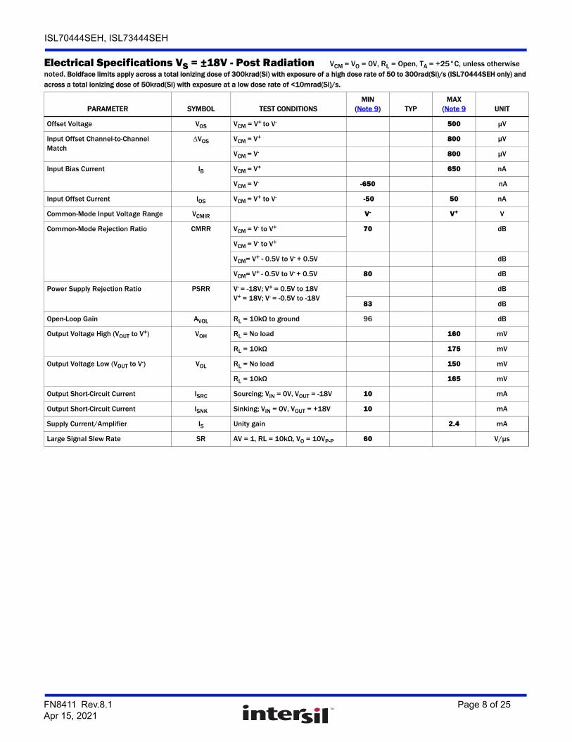
Electrical Specifications VS = ±18V - Post Radiation VCM = VO = 0V, RL = Open, TA = +25°C, unless otherwise noted. Boldface limits apply across a total ionizing dose of 300krad(Si) with exposure of a high dose rate of 50 to 300rad(Si)/s (ISL70444SEH only) and across a total ionizing dose of 50krad(Si) with exposure at a low dose rate of <10mrad(Si)/s.
PARAMETER SYMBOL TEST CONDITIONSMIN
(Note 9) TYPMAX
(Note 9 UNIT
Offset Voltage VOS VCM = V+ to V- 500 µV
Input Offset Channel-to-Channel Match
VOS VCM = V+ 800 µV
VCM = V- 800 µV
Input Bias Current IB VCM = V+ 650 nA
VCM = V- -650 nA
Input Offset Current IOS VCM = V+ to V- -50 50 nA
Common-Mode Input Voltage Range VCMIR V- V+ V
Common-Mode Rejection Ratio CMRR VCM = V- to V+ 70 dB
VCM = V- to V+
VCM= V+ - 0.5V to V- + 0.5V dB
VCM= V+ - 0.5V to V- + 0.5V 80 dB
Power Supply Rejection Ratio PSRR V- = -18V; V+ = 0.5V to 18VV+ = 18V; V- = -0.5V to -18V
dB
83 dB
Open-Loop Gain AVOL RL = 10kΩ to ground 96 dB
Output Voltage High (VOUT to V+) VOH RL = No load 160 mV
RL = 10kΩ 175 mV
Output Voltage Low (VOUT to V-) VOL RL = No load 150 mV
RL = 10kΩ 165 mV
Output Short-Circuit Current ISRC Sourcing; VIN = 0V, VOUT = -18V 10 mA
Output Short-Circuit Current ISNK Sinking; VIN = 0V, VOUT = +18V 10 mA
Supply Current/Amplifier IS Unity gain 2.4 mA
Large Signal Slew Rate SR AV = 1, RL = 10kΩ, VO = 10VP-P 60 V/µs
FN8411 Rev.8.1 Page 8 of 25Apr 15, 2021
ISL70444SEH, ISL73444SEH
Electrical Specifications VS = ±2.5V - Post Radiation VCM = VO = 0V, RL = Open, TA = +25°C, unless otherwise noted. Boldface limits apply a total ionizing dose of 300krad(Si) with exposure of a high dose rate of 50 to 300rad(Si)/s (ISL70444SEH only) and across a total ionizing dose of 50krad(Si) with exposure at a low dose rate of <10mrad(Si)/s.
PARAMETER SYMBOL TEST CONDITIONSMIN
(Note 9) TYPMAX
(Note 9) UNIT
Offset Voltage VOS VCM = V+ to V- 500 µV
Input Offset Channel-to-Channel Match VOS VCM = V+ 800 µV
VCM = V- 800 µV
Input Bias Current IB VCM = V+ 650 nA
VCM = V- -650 nA
Input Offset Current IOS VCM = V+ to V- -50 50 nA
Common-Mode Input Voltage Range VCMIR V- V+ V
Common-Mode Rejection Ratio CMRR VCM = V- to V+ dB
VCM = V- to V+ 70 dB
VCM= V+ - 0.5V to V- + 0.5V dB
VCM= V+ - 0.5V to V- + 0.5V 74 dB
Power Supply Rejection Ratio PSRR V- = -2.5V; V+ = 0.5V to 2.5VV+ = 2.5V; V- = -0.5V to -2.5V
dB
80 dB
Open-loop Gain AVOL RL = 10kΩ to ground 90 dB
Output Voltage High (VOUT to V+) VOH RL = No load 85 mV
RL = 10kΩ 105 mV
RL = 600Ω 400 mV
Output Voltage Low (VOUT to V-) VOL RL = No load 85 mV
RL = 10kΩ 105 mV
RL = 600Ω 400 mV
Supply Current/Amplifier IS Unity gain 1.8 mA
Electrical Specifications VS = ±1.5V - Post Radiation VCM = VO = 0V, RL = Open, TA = +25°C, unless otherwise noted. Boldface limits apply a total ionizing dose of 300krad(Si) with exposure of a high dose rate of 50 to 300rad(Si)/s (ISL70444SEH only) and across a total ionizing dose of 50krad(Si) with exposure at a low dose rate of <10mrad(Si)/s.
PARAMETER SYMBOL TEST CONDITIONSMIN
(Note 9) TYPMAX
(Note 9) UNIT
Offset Voltage VOS VCM = V+ to V- 500 µV
Input Offset Channel-to-Channel Match VOS VCM = V+ 800 µV
VCM = V- 800 µV
Input Bias Current IB VCM = V+ 650 nA
VCM = V- -650 nA
Input Offset Current IOS VCM = V+ to V- -50 50 nA
Common-Mode Input Voltage Range VCMIR V- V+ V
Output Voltage High (VOUT to V+) VOH RL = No load 160 mV
RL = 10kΩ 175 mV
Output Voltage Low (VOUT to V-) VOL RL = No load 150 mV
RL = 10kΩ 165 mV
Supply Current/Amplifier IS Unity gain 1.8 mA
NOTE:9. Compliance to datasheet limits is assured by one or more methods: production test, characterization, and/or design.
FN8411 Rev.8.1 Page 9 of 25Apr 15, 2021
ISL70444SEH, ISL73444SEH
Typical Performance Curves Unless otherwise specified, VS ±18V, VCM = 0, VO = 0V, TA = +25°C.
FIGURE 3. OFFSET VOLTAGE vs COMMON-MODE VOLTAGE FIGURE 4. IBIAS vs COMMON-MODE VOLTAGE
FIGURE 5. IBIAS vs TEMPERATURE (VS = ±18V) FIGURE 6. IBIAS vs TEMPERATURE (VS = ±2.5V)
FIGURE 7. IBIAS vs TEMPERATURE, (VS = ±1.5V) FIGURE 8. IOS vs TEMPERATURE (VS = ±18V)
-60
-40
-20
0
20
40
60
80
100
120
-20 -15 -10 -5 0 5 10 15 20
COMMON MODE VOLTAGE (V)
OF
FS
ET
VO
LT
AG
E (
µV
)
-300
-200
-100
0
100
200
300
-20 -15 -10 -5 0 5 10 15 20
COMMON MODE VOLTAGE (V)
I BIA
S (n
A)
0
50
100
150
200
250
300
-100 -50 0 50 100 150
TEMPERATURE (°C)
IB+
IB-
CU
RR
EN
T (
nA
)
0
50
100
150
200
250
-100 -50 0 50 100 150
TEMPERATURE (°C)
IB+
IB-
CU
RR
EN
T (
nA
)
0
50
100
150
200
250
300
-100 -50 0 50 100 150
TEMPERATURE (°C)
CU
RR
EN
T (
nA
)
IB+
IB-
0
0.5
1.0
1.5
2.0
2.5
-100 -50 0 50 100 150
TEMPERATURE (°C)
CU
RR
EN
T (
nA
)
IOS
FN8411 Rev.8.1 Page 10 of 25Apr 15, 2021
ISL70444SEH, ISL73444SEH
FIGURE 9. IOS vs TEMPERATURE (VS = ±2.5V) FIGURE 10. IOS vs TEMPERATURE (VS = ±1.5V)
FIGURE 11. VOS vs TEMPERATURE (VS = ±18V) FIGURE 12. VOS vs TEMPERATURE (VS = ±2.5V)
FIGURE 13. VOS vs TEMPERATURE (VS = ±1.5V) FIGURE 14. AVOL vs TEMPERATURE vs SUPPLY VOLTAGE
Typical Performance Curves Unless otherwise specified, VS ±18V, VCM = 0, VO = 0V, TA = +25°C. (Continued)
0
0.5
1.0
1.5
2.0
2.5
-100 -50 0 50 100 150
TEMPERATURE (°C)
IOS
CU
RR
EN
T (
nA
)
0
0.5
1.0
1.5
2.0
2.5
3.0
3.5
-100 -50 0 50 100 150
TEMPERATURE (°C)
IOS
CU
RR
EN
T (
nA
)
0
10
20
30
40
50
60
70
-100 -50 0 50 100 150
TEMPERATURE (°C)
VO
LT
AG
E (
µV
)
VOS
0
10
20
30
40
50
60
70
-100 -50 0 50 100 150
TEMPERATURE (°C)
VO
LT
AG
E (
µV
)
VOS
0
10
20
30
40
50
-100 -50 0 50 100 150
TEMPERATURE (°C)
VOS
VO
LT
AG
E (
µV
)
100
105
110
115
120
125
130
135
-75 -25 25 75 125
TEMPERATURE (°C)
±1.5V
GA
IN (
dB
)
±18V
±2.5V
FN8411 Rev.8.1 Page 11 of 25Apr 15, 2021
ISL70444SEH, ISL73444SEH
FIGURE 15. NEGATIVE SUPPLY CURRENT vs SUPPLY VOLTAGE FIGURE 16. POSITIVE SUPPLY CURRENT vs SUPPLY VOLTAGE
FIGURE 17. PSRR+ vs TEMPERATURE vs SUPPLY VOLTAGE FIGURE 18. PSRR- vs TEMPERATURE vs SUPPLY VOLTAGE
FIGURE 19. CMRR vs TEMPERATURE vs SUPPLY VOLTAGE FIGURE 20. SHORT-CIRCUIT CURRENT vs TEMPERATURE
Typical Performance Curves Unless otherwise specified, VS ±18V, VCM = 0, VO = 0V, TA = +25°C. (Continued)
-2.5
-2.0
-1.5
-1.0
-0.5
0.0
0 10 20 30 40
SUPPLY DIFFERENTIAL (V+ TO V-) (V)
CU
RR
EN
T (
mA
)
+125°C
-55°C+25°C
0.0
0.5
1.0
1.5
2.0
2.5
0 10 20 30 40
SUPPLY DIFFERENTIAL (V+ TO V-) (V)
CU
RR
EN
T (
mA
)
-55°C
+125°C
+25°C
100
105
110
115
120
125
130
135
-75 -25 25 75 125
TEMPERATURE (°C)
±1.5V GA
IN (
dB
)
±18V
±2.5V
100
105
110
115
120
125
130
135
-75 -25 25 75 125
TEMPERATURE (°C)
GA
IN (
dB
)±2.5V
±18V
±1.5V
40
50
60
70
80
90
100
110
120
-75 -25 25 75 125
TEMPERATURE (°C)
GA
IN (
dB
)
±1.5V ±2.5V
±18V
0
10
20
30
40
50
60
70
-75 -25 25 75 125
TEMPERATURE (°C)
CU
RR
EN
T (
mA
)
±15V
±2.5V
±1.5V
±5V ±18V
FN8411 Rev.8.1 Page 12 of 25Apr 15, 2021
ISL70444SEH, ISL73444SEH
FIGURE 21. (VS = ±1.5V) VOH vs TEMPERATURE FIGURE 22. (VS = ±2.5V) VOH vs TEMPERATURE
FIGURE 23. (VS = ±18V) VOH vs TEMPERATURE FIGURE 24. (VS = ±1.5V) VOL vs TEMPERATURE
FIGURE 25. (VS = ±2.5V) VOL vs TEMPERATURE FIGURE 26. (VS = ±18V) VOL vs TEMPERATURE
Typical Performance Curves Unless otherwise specified, VS ±18V, VCM = 0, VO = 0V, TA = +25°C. (Continued)
0
10
20
30
40
50
-75 -25 25 75 125 175
TEMPERATURE (°C)
(VS
+ -
VO
UT)
(mV
)
RL = 2kΩ
RL = OPEN
RL = 10kΩ
0
10
20
30
40
50
60
70
-75 -25 25 75 125 175
(VS
+ -
VO
UT)
(mV
)
TEMPERATURE (°C)
RL = 2kΩ
RL = OPEN
RL = 10kΩ
0
50
100
150
200
250
300
350
-75 -25 25 75 125 175
TEMPERATURE (°C)
(VS
+ -
VO
UT)
(mV
)
RL = 2kΩ
RL = OPENRL = 10kΩ
0
10
20
30
40
50
TEMPERATURE (°C)
(VS
- + V
OU
T)
(mV
)RL = 2kΩ
RL = OPEN
RL = 10kΩ
-75 -25 25 75 125 175
0
10
20
30
40
50
60
70
-75 -25 25 75 125 175
TEMPERATURE (°C)
(VS
- + V
OU
T)
(mV
)
RL = 2kΩ
RL = OPEN
RL = 10kΩ
0
50
100
150
200
250
300
350
-75 -25 25 75 125 175
TEMPERATURE (°C)
(VS
- - V
OU
T)
(mV
)
RL = 2kΩ
RL = OPENRL = 10kΩ
FN8411 Rev.8.1 Page 13 of 25Apr 15, 2021
ISL70444SEH, ISL73444SEH
FIGURE 27. INPUT NOISE VOLTAGE SPECTRAL DENSITY (VS = ±18V) FIGURE 28. INPUT NOISE CURRENT SPECTRAL DENSITY (VS = ±18V)
FIGURE 29. OPEN LOOP FREQUENCY RESPONSE (CL = 0.01pF) FIGURE 30. OPEN LOOP FREQUENCY RESPONSE (CL = 10pF)
FIGURE 31. OPEN LOOP FREQUENCY RESPONSE (CL = 22pF) FIGURE 32. OPEN LOOP FREQUENCY RESPONSE (CL = 47pF)
Typical Performance Curves Unless otherwise specified, VS ±18V, VCM = 0, VO = 0V, TA = +25°C. (Continued)
1
10
100
1,000
10,000
0.01 0.1 1 10 100 1k 10k 100k
FREQUENCY (Hz)
INP
UT
NO
ISE
VO
LT
AG
E (
nV
/√H
z)
0.1
1
10
0.1 1 10 100 1k 10k 100k
FREQUENCY (Hz)
INP
UT
NO
ISE
CU
RR
EN
T (
pA
/√H
z)
-250
-200
-150
-100
-50
0
50
100
150
200
-150
-100
-50
0
50
100
150
0 10 1k 100k 10M 1G
FREQUENCY (Hz)
SIMULATION
GA
IN (
dB
)
PH
AS
E (
°)
GAIN
PHASE
-300
-250
-200
-150
-100
-50
0
50
100
150
200
250
-150
-100
-50
0
50
100
150
0 10 1k 100k 10M 1G
FREQUENCY (Hz)
SIMULATION
GA
IN (
dB
)
GAIN
PHASE
PH
AS
E (
°)
-300
-250
-200
-150
-100
-50
0
50
100
150
200
250
-150
-100
-50
0
50
100
150
0 10 1k 100k 10M 1G
FREQUENCY (Hz)
SIMULATION
GA
IN (
dB
)
PH
AS
E (
°)
GAIN
PHASE
-300
-250
-200
-150
-100
-50
0
50
100
150
200
250
-150
-100
-50
0
50
100
150
0 10 1k 100k 10M 1G
SIMULATION
GA
IN (
dB
)
PH
AS
E (
°)
GAIN
PHASE
FREQUENCY (Hz)
FN8411 Rev.8.1 Page 14 of 25Apr 15, 2021
ISL70444SEH, ISL73444SEH
FIGURE 33. OPEN LOOP FREQUENCY RESPONSE (CL = 100pF) FIGURE 34. CMRR vs FREQUENCY
FIGURE 35. PSRR vs FREQUENCY, ±18V FIGURE 36. PSRR vs FREQUENCY, ±2.5V
FIGURE 37. PSRR vs FREQUENCY, ±1.5V FIGURE 38. FREQUENCY RESPONSE vs CLOSED LOOP GAIN
Typical Performance Curves Unless otherwise specified, VS ±18V, VCM = 0, VO = 0V, TA = +25°C. (Continued)
-300
-250
-200
-150
-100
-50
0
50
100
150
200
250
-150
-100
-50
0
50
100
150
0 10 1k 100k 10M 1GFREQUENCY (Hz)
SIMULATION
GA
IN (
dB
)
PH
AS
E (
°)
GAIN
PHASE
-10 0
10 20 30 40 50 60 70 80 90
100 110 120 130 140
100 1k 10k 100k 1M 10M 100M
FREQUENCY (Hz)
GA
IN (
dB
)
±1.5V
±18V
±2.5V
FREQUENCY (Hz)
0
20
40
60
80
100
120
140
160
1k 10k 100k 1M 10M10 100
-55°C
125°C
25°C
PS
RR
(d
B)
0
20
40
60
80
100
120
140
160
1k 10k 100k 1M 10M
FREQUENCY (Hz)
10 100
-55°C
25°C
125°C
PS
RR
(d
B)
0
20
40
60
80
100
120
140
160
1k 10k 100k 1M 10M
FREQUENCY (Hz)
10 100
-55°C
125°C
25°C
PS
RR
(d
B)
-50
-40
-30
-20
-10
0
10
20
30
40
50
60
70
100 1k 10k 100k 1M 10M 100M
FREQUENCY (Hz)
GA
IN (
dB
)
G = 10
G = 1000
G = 100
G = 1
FN8411 Rev.8.1 Page 15 of 25Apr 15, 2021
ISL70444SEH, ISL73444SEH
FIGURE 39. FREQUENCY RESPONSE vs FEEDBACK RESISTANCE (RF) FIGURE 40. FREQUENCY RESPONSE vs LOAD RESISTANCE
FIGURE 41. UNITY GAIN RESPONSE vs LOAD CAPACITANCE FIGURE 42. FREQUENCY RESPONSE vs SUPPLY VOLTAGE
FIGURE 43. CROSSTALK REJECTION FIGURE 44. SLEW RATE vs STEP SIZE vs TEMPERATURE (VS = ±1.5V)
Typical Performance Curves Unless otherwise specified, VS ±18V, VCM = 0, VO = 0V, TA = +25°C. (Continued)
-70
-60
-50
-40
-30
-20
-10
0
10
20
100 1k 10k 100k 1M 10M 100M
FREQUENCY (Hz)
GA
IN (
dB
)
RF = 10kΩ
RF = 100Ω
RF = 1kΩ
-30
-20
-10
0
10
100 1k 10k 100k 1M 10M 100M
FREQUENCY (Hz)
RL = 5kΩ
RL = 1kΩRL = 10kΩ RL = 2kΩ
GA
IN (
dB
)
-50
-40
-30
-20
-10
0
10
100 1k 10k 100k 1M 10M 100M
FREQUENCY (Hz)
ACL = 1 RL = 10kΩVS = ±18V
GA
IN (
dB
)
12pF
27pF
47pF
68pF
-40
-30
-20
-10
0
10
100 1k 10k 100k 1M 10M 100M
FREQUENCY (Hz)
GA
IN (
dB
) ±1.5V
±18V
±2.5V
0 10 20 30 40 50 60 70 80 90
100 110 120 130 140
100 1k 10k 100k 1M 10M 100MFREQUENCY (Hz)
GA
IN (
dB
) ±1.5V
±18V±2.5V
0
5
10
15
20
25
30
35
0.0 0.5 1.0 1.5 2.0 2.5 3.0 3.5 STEP SIZE (V)
SL
EW
RA
TE
(V
/µs
)
-55°C
+25°C
+125°C
FN8411 Rev.8.1 Page 16 of 25Apr 15, 2021
ISL70444SEH, ISL73444SEH
FIGURE 45. SLEW RATE vs STEP SIZE vs TEMPERATURE (VS = ±2.5V) FIGURE 46. SLEW RATE vs STEP SIZE vs TEMPERATURE (VS = ±18V)
Typical Performance Curves Unless otherwise specified, VS ±18V, VCM = 0, VO = 0V, TA = +25°C. (Continued)
10µs/DIV
VS = ±5V2V/DIV, OUTPUTVIN = 12VP-PNo Output Phase Reversal
2V/DIV, INPUT
Post High Dose Rate Radiation Characteristics Unless otherwise specified, VS ±18V, VCM = 0, VO = 0V, TA = +25°C. This data is typical mean test data post radiation exposure at a high dose rate of 50 to 300rad(Si)/s (ISL70444SEH only). This data is intended to show typical parameter shifts due to high dose rate radiation. These are not limits nor are they guaranteed.
FIGURE 52. VOS SHIFT vs HIGH DOSE RATE RADIATION FIGURE 53. IBIAS SHIFT vs HIGH DOSE RATE RADIATION
FIGURE 54. I- SHIFT vs HIGH DOSE RATE RADIATION FIGURE 55. I+ SHIFT vs HIGH DOSE RATE RADIATION
-30
-20
-10
0
10
20
30
0 50 100 150 200 250 300
krad (Si)
V OS
(µV
)
VS = ±18V
GROUNDED
BIASED
-30
-20
-10
0
10
20
30
0 50 100 150 200 250 300
krad (Si)
CU
RR
EN
T (
nA
)VS = ±18V
GROUNDED
BIASED
-0.8
-0.6
-0.4
-0.2
0
0.2
0.4
0.6
0.8
0 50 100 150 200 250 300
krad (Si)
CU
RR
EN
T (
mA
)
VS = ±18V
BIASED
GROUNDED
-0.8
-0.6
-0.4
-0.2
0
0.2
0.4
0.6
0.8
0 50 100 150 200 250 300
krad (Si)
CU
RR
EN
T (
mA
)
VS = ±18V
BIASED
GROUNDED
FN8411 Rev.8.1 Page 18 of 25Apr 15, 2021
ISL70444SEH, ISL73444SEH
FIGURE 56. IOS SHIFT vs HIGH DOSE RATE RADIATION
Post High Dose Rate Radiation Characteristics Unless otherwise specified, VS ±18V, VCM = 0, VO = 0V, TA = +25°C. This data is typical mean test data post radiation exposure at a high dose rate of 50 to 300rad(Si)/s (ISL70444SEH only). This data is intended to show typical parameter shifts due to high dose rate radiation. These are not limits nor are they guaranteed.
-2.0
-1.5
-1.0
-0.5
0
0.5
1.0
1.5
2.0
0 50 100 150 200 250 300
krad (Si)
CU
RR
EN
T (
nA
)
VS = ±18V
BIASED
GROUNDED
Post Low Dose Rate Radiation Characteristics Unless otherwise specified, VS ±18V, VCM = 0, VO = 0V, TA = +25°C. This data is typical mean test data post radiation exposure at a low dose rate of <10mrad(Si)/s. This data is intended to show typical parameter shifts due to high dose rate radiation. These are not limits nor are they guaranteed.
FIGURE 57. VOS SHIFT vs LOW DOSE RATE RADIATION FIGURE 58. IBIAS SHIFT vs LOW DOSE RATE RADIATION
FIGURE 59. IOS SHIFT vs LOW DOSE RATE RADIATION FIGURE 60. I+ SHIFT vs LOW DOSE RATE RADIATION
-30
-20
-10
0
10
20
30
0 10 20 30 40 50 60 70 80 90 100 krad (Si)
VS = ±18V
V OS
(µV
)
BIASED
GROUNDED
-30
-20
-10
0
10
20
30
0 10 20 30 40 50 60 70 80 90 100 krad (Si)
CU
RR
EN
T (
nA
)
VS = ±18V
BIASED
GROUNDED
-6
-4
-2
0
2
4
6
0 10 20 30 40 50 60 70 80 90 100
krad (Si)
CU
RR
EN
T (
nA
)
VS = ±18V
BIASED
GROUNDED
-0.8
-0.6
-0.4
-0.2
0
0.2
0.4
0.6
0.8
0 10 20 30 40 50 60 70 80 90 100
krad (Si)
CU
RR
EN
T (
mA
)
VS = ±18V
BIASED
GROUNDED
FN8411 Rev.8.1 Page 19 of 25Apr 15, 2021
ISL70444SEH, ISL73444SEH
Applications InformationFunctional DescriptionThe ISL7x444SEH contain four high-speed and low-power op amps designed to take advantage of their full dynamic input and output voltage range with rail-to-rail operation. By offering low power, low offset voltage and low temperature drift coupled with its high bandwidth and enhanced slew rates upwards of 50V/µs, these op amps are ideal for applications requiring both high DC accuracy and AC performance. The ISL7x444SEH are manufactured using the Renesas PR40 silicon-on-insulator process, which makes these devices immune to single event latch-up and provides excellent radiation tolerance. These features make the devices an ideal choice for high reliability applications in harsh radiation-prone environments.
Operating Voltage RangeThe ISL7x444SEH are designed to operate with a split supply rail from ±1.35V to ±20V or a single supply rail from 2.7V to 40V. The ISL7x444SEH are fully characterized in production for supply rails of 5V (±2.5V) and 36V (±18V). The power supply rejection ratio is typically 120dB over the full operating voltage range. The worst case Common-Mode Rejection Ratio (CMRR) across temperature is within 1.5V to 2V of each rail. When VCM is inside that range, the CMRR performance is typically >110dB with a ±18V supply. The minimum CMRR performance across the -55°C to +125°C temperature range and radiation is >70dB over the full common-mode input range for power supply voltages from ±2.5V (5V) to ±18V (36V).
Input PerformanceThe slew enhanced front-end is a block that is placed in parallel with the main input stage and functions based on the input differential.
Input ESD Diode Protection The input terminals (IN+ and IN-) have internal ESD protection diodes to the positive and negative supply rails, series connected
600Ω current limiting resistors and an anti-parallel diode pair across the inputs.
Output Short-Circuit Current LimitingThe output current limit has a worst case minimum limit of ±10mA but may reach as high as ±100mA. The op amp can withstand a short-circuit to either rail for a short duration (<1s) as long as the maximum operating junction temperature is not violated. This applies to only one amplifier at a given time. Continued use of the device in these conditions may degrade the long term reliability of the part and is not recommended. Figure 20 shows the typical short-circuit currents that can be expected. The ISL7x444SEH’s current limiting circuitry automatically lowers the current limit of the device if short-circuit conditions carry on for extended periods of time. This protects the device from malfunction; however, extended operation in this mode degrades the output rail-to-rail performance by increasing the VOH/VOL levels.
Output Phase Reversal Output phase reversal is a change of polarity in the amplifier transfer function when the input voltage exceeds the supply voltage. The ISL7x444SEH are immune to output phase reversal, even when the input voltage is 1V beyond the supplies. This is illustrated in Figure 51.
FIGURE 61. I- SHIFT vs LOW DOSE RATE RADIATION
Post Low Dose Rate Radiation Characteristics Unless otherwise specified, VS ±18V, VCM = 0, VO = 0V, TA = +25°C. This data is typical mean test data post radiation exposure at a low dose rate of <10mrad(Si)/s. This data is intended to show typical parameter shifts due to high dose rate radiation. These are not limits nor are they guaranteed.
-0.8
-0.6
-0.4
-0.2
0
0.2
0.4
0.6
0.8
0 10 20 30 40 50 60 70 80 90 100 krad (Si)
CU
RR
EN
T (
mA
)
VS = ±18V
BIASED
GROUNDED
FIGURE 62. INPUT ESD DIODE CURRENT LIMITING, UNITY GAIN
-
+ RLVIN
VOUT
V+
V-
600Ω
600Ω
FN8411 Rev.8.1 Page 20 of 25Apr 15, 2021
ISL70444SEH, ISL73444SEH
Power DissipationIt is possible to exceed the +150°C maximum junction temperature under certain load and power supply conditions. It is therefore important to calculate the maximum junction temperature (TJMAX) for all applications to determine if power supply voltages, load conditions, or package type need to be modified to remain in the safe operating range. These parameters are related using Equation 1:
where:
• PDMAXTOTAL is the sum of the maximum power dissipation of each amplifier in the package (PDMAX)
• Calculate PDMAX for each amplifier using Equation 2:
where:
• TMAX = Maximum ambient temperature
• JA = Thermal resistance of the package
• PDMAX = Maximum power dissipation of one amplifier
• VS = Total supply voltage
• IqMAX = Maximum quiescent supply current of one amplifier
• VOUTMAX = Maximum output voltage swing of the application
Slew Rate EnhancementThe ISL7x444SEH have slew enhanced front-end that increases the drive on the output transistors proportional to the differential voltage across the inputs. This increase in output drive shows up as increased transient current on top of the op amp’s steady state supply current. If the voltage differential between the inputs remains constant, as in comparator applications, the added drive current to the output transistors becomes steady state and increases the DC power supply current of the IC. For this reason, we do not recommended using the ISL7x444SEH in a comparator configuration.
Unused Channel ConfigurationIf the application does not require the use of all four op amps, you must configure the unused channels to prevent it from oscillating. Any unused channels oscillate if the input and output pins are floating. The oscillationresults in higher than expected supply currents and possible noise injection into any of the active channels in use. The proper way to prevent oscillation is to short the output to the inverting input and tie the positive input to a known voltage, such as mid-supply.
When the V- supply is less than or equal to -1.0V, configure your op amp as in Figure 63, or follow the configuration shown in Figure 64. The resistors in Figure 64 are of equal value and high resistance (≥10kΩ) to minimize current draw, while keeping the positive input at mid-supply. All unused op amps can have their inputs tied to the same resistor divider to minimize the number of components.
Tying the positive input to ground in Figure 64 (where V- = GND) would produce a voltage differential across the inputs, as the inverting input would be at the op amp’s VOL and the positive input would be at GND, causing an increase in the steady state supply current. While this does not damage the op amp, the increased supply current would result in additional unnecessary power dissipation.
TJMAX TMAX JA x PDMAXTOTAL+= (EQ. 1)
PDMAX VS IqMAX VS - VOUTMAX VOUTMAX
RL----------------------------+= (EQ. 2)
FIGURE 63. PREVENTING OSCILLATIONS IN UNUSED CHANNELS, SPLIT SUPPLY
FIGURE 64. PREVENTING OSCILLATIONS IN UNUSED CHANNELS, SINGLE SUPPLY
V+
V-
V+
V-
FN8411 Rev.8.1 Page 21 of 25Apr 15, 2021
ISL70444SEH, ISL73444SEH
Die CharacteristicsDie Dimensions
2410µm x 3175µm (95 mils x 125 mils)Thickness: 483µm ±25µm (19 mils ±1 mil)
Interface Materials
GLASSIVATIONType: NitroxThickness: 15kÅ
TOP METALLIZATIONType: AlCu (99.5%/0.5%)Thickness: 30kÅ
BACKSIDE FINISH Silicon
PROCESSPR40
Assembly Related InformationSUBSTRATE POTENTIALFloating
Additional Information
WORST CASE CURRENT DENSITY< 2 x 10⁵ A/cm2
TRANSISTOR COUNT730
Weight of Packaged Device0. 5952 grams (Typical)
Lid CharacteristicsFinish: GoldPotential: Unbiased, tied to E-pad under packageCase Isolation to Any Lead: 20 x 109 Ω (min)
Metallization Mask Layout
FN8411 Rev.8.1 Page 22 of 25Apr 15, 2021
ISL70444SEH, ISL73444SEH
Revision History
TABLE 1. DIE LAYOUT X-Y COORDINATES
PAD NAME PAD NUMBER X (µm) Y (µm) dX (µm) dY (µm)BOND WIRES
PER PAD
OUTB 2 599.0 -11.5 70 70 1
OUTC 3 1472.0 -11.5 70 70 1
-INC 4 2071.0 0.0 70 70 1
+INC 12 2071.0 347.5 70 70 1
V- 20 2071.0 1406.5 70 70 1
+IND 21 2071.0 2465.5 70 70 1
-IND 22 2071.0 2813.0 70 70 1
OUTD 23 1472.0 2824.5 70 70 1
OUTA 24 599.0 2824.5 70 70 1
-INA 25 0.0 2813.0 70 70 1
+INA 33 0.0 2465.5 70 70 1
V+ 41 0.0 1406.5 70 70 1
+INB 42 0.0 347.5 70 70 1
-INB 1 0.0 0.0 70 70 1
NOTE:10. Origin of coordinates is the centroid of pad 42, “IN-B”.
The revision history provided is for informational purposes only and is believed to be accurate, but not warranted. Please visit our website to make sure that you have the latest revision.
DATE REVISION CHANGE
Apr 15, 2021 8.1 Changed ±8mA to ±10mA in the Output Short-Circuit Current Limiting section on page 20.
Nov 16, 2020 8.0 Updated Note 3 and added Note 4.Updated Power Supply Rejection Ratio typical from 128 to 143 in the ±18V EC specification table.Updated Power Supply Rejection Ratio typical from 123 to 135 in the ±2.5V EC specification table.Updated Figure 35 and added Figures 36 and 37.
Aug 16, 2019 7.0 Updated SEE and TID ratings in Features section.Added radiation levels to ordering information table.Removed Table 1.
Mar 28, 2019 6.0 Updated links throughout document.Added ISL73444SEH information throughout document.Added Table 1.Updated Disclaimer.
Jan 19, 2018 5.0 Added “Slew Rate Enhancement” section on page 20.On page 21 - Updated “Unused Channel Configuration” section, updated Figure 61 and added Figure 62.Removed “About Intersil” section.Added new disclaimer.
FN8411 Rev.8.1 Page 23 of 25Apr 15, 2021
ISL70444SEH, ISL73444SEH
Jul 6, 2017 4.0 Updated Related Literature section.Changed low input voltage from 300µV to 400µV in features list.Added Notes 3 and 4. Electrical Specification updates:
VS = ±18V table:Updated Offset Voltage from “300” to “400” and “400” to “500”.Updated Input Offset Current from “-17” to “-30” (min) and “17” to “30” (max) unbolded values.Added another Input Offset Current line and bolded.Updated PSRR min from “88” to “83”VS = ±2.5V table:Updated Offset Voltage from “300” to “400” and “400” to “500”.Updated Input Offset Current from “-17” to “-30” (min) and “17” to “30” (max) unbolded values.Added another Input Offset Current line and bolded.Unbolded PSRR min value and added a new line with 70 min bolded.VS = ±1.5V table:Updated Offset Voltage from “300” to “400” and “400” to “500”.Updated Input Offset Current from “-17” to “-30” (min) and “17” to “30” (max) unbolded values.Added another Input Offset Current line and bolded.VS = ±18V table (RAD):Updated Offset Voltage from “400” to “500”.Updated Input Offset Current from “-17” to “-50” (min) and “17” to “50” (max).Updated PSRR min from “88” to “83”VS = ±2.5V table (RAD):Updated Offset Voltage from “400” to “500”.Updated Input Offset Current from “-17” to “-50” (min) and “17” to “50” (max).VS = ±1.5V table (RAD):Updated Offset Voltage from “400” to “500”.Updated Input Offset Current from “-17” to “-50” (min) and “17” to “50” (max).
Jun 5, 2015 3.0 Changed Die Dimensions on page 22:From2410µm x 3175µm (80mils x 101mils) Thickness: 483µm ± 25µm (19mils ± 1 mil)To:Die Dimensions2410µm x 3175µm (95mils x 125mils) Thickness: 483µm ± 25µm (19mils ± 1 mil)
Jun 14, 2013 1.0 Changed Radiation tolerance High dose rate from 100krad(Si) to 300krad(Si) on page 1 features and in Electrical Spec Table conditions on pages 7 and 8.Added SR spec for VS = ±18V to Electrical Spec Table on page 8.Removed Max limit of 300 for VOS Offset Voltage in VS = ±18V, VS = ±2.5V and VS = ±1.5V Spec tables.
May 23, 2013 0.0 Initial Release.
The revision history provided is for informational purposes only and is believed to be accurate, but not warranted. Please visit our website to make sure that you have the latest revision. (Continued)
DATE REVISION CHANGE
FN8411 Rev.8.1 Page 24 of 25Apr 15, 2021
ISL70444SEH, ISL73444SEH
Package Outline DrawingK14.C14 Lead Ceramic Metal Seal Flatpack Package Rev 0, 9/12
SIDE VIEW
TOP VIEW
SECTION A-A
-D-
-C-
SEATING AND
BASE PLANE
-H-
BASE
METAL
PIN NO. 1
ID AREA
0.022 (0.56)
0.015 (0.38)
0.050 (1.27 BSC)
0.005 (0.13)MIN
0.115 (2.92)
0.085 (2.16) 0.045 (1.14)
0.026 (0.66) 0.260 (6.60)
0.248 (6.30)
0.009 (0.23)
0.004 (0.10)
0.370 (9.40)
0.270 (6.86)
0.03 (0.76) MIN
0.006 (0.15)
0.004 (0.10)
0.009 (0.23)
0.004 (0.10)
0.019 (0.48)
0.015 (0.38)
0.0015 (0.04)MAX
0.022 (0.56)
0.015 (0.38)
3
5
2
LEAD FINISH
1.adjacent to pin one and shall be located within the shaded area shown. The manufacturer’s identification shall not be used as a pin one identification mark.
2. The maximum limits of lead dimensions (section A-A) shall be measured at the centroid of the finished lead surfaces, when solder dip or tin plate lead finish is applied.
3.
4.shall be molded to the bottom of the package to cover the leads.
5.meniscus) of the lead from the body. Dimension minimum shall be reduced by 0.0015 inch (0.038mm) maximum when solder diplead finish is applied.
7.
8.
NOTES:
Dimensioning and tolerancing per ANSI Y14.5M - 1982.
Dimensions: INCH (mm). Controlling dimension: INCH.
Index area: A notch or a pin one identification mark shall be located
Measure dimension at all four corners.
For bottom-brazed lead packages, no organic or polymeric materials
Dimension shall be measured at the point of exit (beyond the
0.390 (9.91)
0.376 (9.55)
0.183 (4.65)
0.167 (4.24)
6
BOTTOM
METAL
6. The bottom of the package is a solderable metal surface.
BOTTOM VIEW
OPTIONAL
PIN 1 INDEX
BOTTOM METAL
0.005 (0.127) REF.
OFFSET FROM
CERAMIC EDGE
A
A
1
For the most recent package outline drawing, see K14.C.
Corporate HeadquartersTOYOSU FORESIA, 3-2-24 Toyosu,Koto-ku, Tokyo 135-0061, Japanwww.renesas.com
Contact InformationFor further information on a product, technology, the most up-to-date version of a document, or your nearest sales office, please visit:www.renesas.com/contact/
TrademarksRenesas and the Renesas logo are trademarks of Renesas Electronics Corporation. All trademarks and registered trademarks are the property of their respective owners.
IMPORTANT NOTICE AND DISCLAIMER
RENESAS ELECTRONICS CORPORATION AND ITS SUBSIDIARIES (“RENESAS”) PROVIDES TECHNICAL SPECIFICATIONS AND RELIABILITY DATA (INCLUDING DATASHEETS), DESIGN RESOURCES (INCLUDING REFERENCE DESIGNS), APPLICATION OR OTHER DESIGN ADVICE, WEB TOOLS, SAFETY INFORMATION, AND OTHER RESOURCES “AS IS” AND WITH ALL FAULTS, AND DISCLAIMS ALL WARRANTIES, EXPRESS OR IMPLIED, INCLUDING, WITHOUT LIMITATION, ANY IMPLIED WARRANTIES OF MERCHANTABILITY, FITNESS FOR A PARTICULAR PURPOSE, OR NON-INFRINGEMENT OF THIRD PARTY INTELLECTUAL PROPERTY RIGHTS.
These resources are intended for developers skilled in the art designing with Renesas products. You are solely responsible for (1) selecting the appropriate products for your application, (2) designing, validating, and testing your application, and (3) ensuring your application meets applicable standards, and any other safety, security, or other requirements. These resources are subject to change without notice. Renesas grants you permission to use these resources only for development of an application that uses Renesas products. Other reproduction or use of these resources is strictly prohibited. No license is granted to any other Renesas intellectual property or to any third party intellectual property. Renesas disclaims responsibility for, and you will fully indemnify Renesas and its representatives against, any claims, damages, costs, losses, or liabilities arising out of your use of these resources. Renesas' products are provided only subject to Renesas' Terms and Conditions of Sale or other applicable terms agreed to in writing. No use of any Renesas resources expands or otherwise alters any applicable warranties or warranty disclaimers for these products.