User's GuideSLLU207A–August 2014–Revised September 2015
ISO5852S Evaluation Module
The manual describes the ISO5852S Evaluation Module (EVM). The ISO5852S EVM allows designers toevaluate device AC and DC performance with a pre-populated 1-nF load or with a user-installed IGBT ineither of the standard TO-247 or TO-220 packages.
Warning: Note that although these devices provide galvanic isolation of upto 5700 V, the EVM cannot be used for isolation voltage testing. Voltageexceeding the EVM’s ratings (VCC1 > 5.5 V, VCC2 – VEE2 > 30 V, or IGBTCollector-Emitter Voltage VCE > 50 V) can damage the EVM resulting inpersonal injury.
Contents1 Overview ...................................................................................................................... 32 EVM Setup and Precautions ............................................................................................... 3
2.1 Before You Begin ................................................................................................... 32.2 Power Supply Connections........................................................................................ 42.3 Signal Connections ................................................................................................. 5
3 Example Measurements .................................................................................................... 64 Printed-Circuit Board....................................................................................................... 10
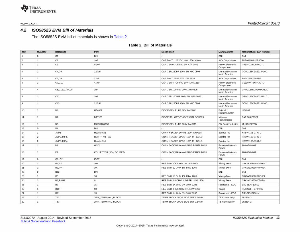
4.1 ISO5852S Operation.............................................................................................. 114.2 ISO5852S EVM Bill of Materials ................................................................................ 13
List of Figures
1 ISO5852S EVM Power Supply Schematic ............................................................................... 42 Output Power Supply for Unipolar (Left) or Bipolar (Right) Operation................................................ 43 ISO5852S EVM Signal Path Schematic .................................................................................. 54 ISO5852S EVM Input and Output With Unipolar Output Supply ...................................................... 65 ISO5852S EVM Input and Output With Bipolar Output Supply (VCC2 = 15 V, VEE2 = –8 V)......................... 76 ISO5852S EVM OUTH/L, DESAT, FLT, and RST With Unipolar Output Supply ................................... 77 ISO5852S EVM OUTH/L, RDY, FLT, and RST With Unipolar Output Supply....................................... 88 ISO5852S EVM OUTH/L, DESAT, FLT, and RST With Bipolar Output Supply ..................................... 89 ISO5852S EVM OUTH/L, RDY, FLT, and RST With Bipolar Output Supply ........................................ 910 ISO5852S EVM ............................................................................................................ 10
List of Tables
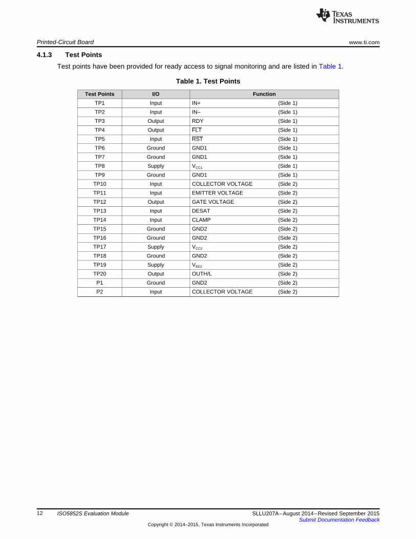
1 Test Points .................................................................................................................. 122 Bill of Materials ............................................................................................................. 13
All trademarks are the property of their respective owners.
1SLLU207A–August 2014–Revised September 2015 ISO5852S Evaluation ModuleSubmit Documentation Feedback
General Texas Instruments High Voltage Evaluation (TI HV EVM) User Safety Guidelines
WARNING
Always follow TI’s set-up and application instructions, including use of all interface components within theirrecommended electrical rated voltage and power limits. Always use electrical safety precautions to helpensure your personal safety and the safety of those working around you. Contact TI’s Product InformationCenter http://support/ti./com for further information.
Save all warnings and instructions for future reference.Failure to follow warnings and instructions may result in personal injury, property damage, ordeath due to electrical shock and/or burn hazards.The term TI HV EVM refers to an electronic device typically provided as an open framed, unenclosedprinted circuit board assembly. It is intended strictly for use in development laboratory environments,solely for qualified professional users having training, expertise, and knowledge of electrical safety risks indevelopment and application of high-voltage electrical circuits. Any other use and/or application are strictlyprohibited by Texas Instruments. If you are not suitably qualified, you should immediately stop from furtheruse of the HV EVM.1. Work Area Safety:
(a) Keep work area clean and orderly.(b) Qualified observer(s) must be present anytime circuits are energized.(c) Effective barriers and signage must be present in the area where the TI HV EVM and its interface
electronics are energized, indicating operation of accessible high voltages may be present, for thepurpose of protecting inadvertent access.
(d) All interface circuits, power supplies, evaluation modules, instruments, meters, scopes and otherrelated apparatus used in a development environment exceeding 50 VRMS/75 VDC must beelectrically located within a protected Emergency Power Off (EPO) protected power strip.
(e) Use a stable and non-conductive work surface.(f) Use adequately insulated clamps and wires to attach measurement probes and instruments. No
freehand testing whenever possible.2. Electrical Safety:As a precautionary measure, it is always a good engineering practice to assume that
the entire EVM may have fully accessible and active high voltages.(a) De-energize the TI HV EVM and all its inputs, outputs, and electrical loads before performing any
electrical or other diagnostic measurements. Revalidate that TI HV EVM power has been safely de-energized.
(b) With the EVM confirmed de-energized, proceed with required electrical circuit configurations, wiring,measurement equipment hook-ups and other application needs, while still assuming the EVM circuitand measuring instruments are electrically live.
(c) Once EVM readiness is complete, energize the EVM as intended.WARNING: while the EVM is energized, never touch the EVM or its electrical circuits as theycould be at high voltages capable of causing electrical shock hazard.
3. Personal Safety:(a) Wear personal protective equipment, for example, latex gloves and/or safety glasses with side
shields or protect EVM in an adequate lucent plastic box with interlocks from accidental touch.4. Limitation for Safe Use:
(a) EVMs are not to be used as all or part of a production unit.
2 ISO5852S Evaluation Module SLLU207A–August 2014–Revised September 2015Submit Documentation Feedback
1 OverviewThe ISO5852S is a 5.7-kVRMS, reinforced isolated, IGBT gate driver with split outputs, OUTH and OUTL,providing 2.5-A source and 5-A sink currents. The input side operates from a single 2.25-V to 5.5-Vsupply. The output side allows for a supply range from minimum 15 V to maximum 30 V. Twocomplementary CMOS inputs control the output state of the gate driver. The short propagation timeassures accurate control of the output stage.
An internal desaturation detection recognizes when the IGBT is in an overload condition. Upon adesaturation detect, a Mute logic immediately blocks the output of the isolator and initiates a soft-turn-offprocedure which disables, OUTH, and pulls OUTL to low over a time span of 2 μs. When OUTL reaches2 V with respect to the most negative supply potential, VEE2, the gate driver output is pulled hard to VEE2potential, turning the IGBT immediately off.
When desaturation is active, a fault signal is sent across the isolation barrier pulling the FLT output at theinput side low and blocking the isolator input. Mute logic is activated through the soft-turn-off period. TheFLT output condition is latched and can be reset only after RDY goes high, through a low-active pulse atthe RST input.
When the IGBT is turned off during normal operation with bipolar output supply, the output is hard clampto VEE2. If the output supply is unipolar, an active Miller clamp can be used, allowing Miller current to sinkacross a low impedance path preventing IGBT to be dynamically turned on during high voltage transientconditions.
The readiness for the gate driver to be operated is under the control of two undervoltage-lockout circuitsmonitoring the input and output supplies. If either side have insufficient supply, the RDY output goes low,otherwise the output is high.
2 EVM Setup and Precautions
2.1 Before You BeginThe following warnings and cautions are noted for the safety of anyone using or working close to theISO5852S EVM. Observe all safety precautions.
Warning Warning Hot surface. Contact may cause burns. Do not touch.
Danger High The ISO5852S EVM does not have an isolation boundary. If you applyVoltage high voltage to this board, all terminals should be considered high voltage.
spacerElectric shock is possible when connecting the board to live wire. Theboard should be handled with care by a professional.spacerFor safety, use of isolated test equipment with overvoltage andovercurrent protection is highly recommended.
3SLLU207A–August 2014–Revised September 2015 ISO5852S Evaluation ModuleSubmit Documentation Feedback
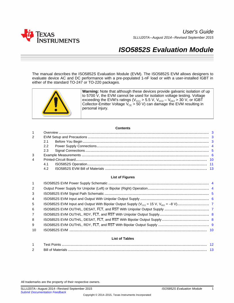
2.2 Power Supply ConnectionsFigure 1 illustrates the ISO5852S EVM power supply schematic.
Figure 1. ISO5852S EVM Power Supply Schematic
The input side of the ISO5852S EVM (VCC1) operates from a single 2.25-V to 5.5-V power supply andconnected via TB3. Test point (TP8) is available for monitoring the input power supply.
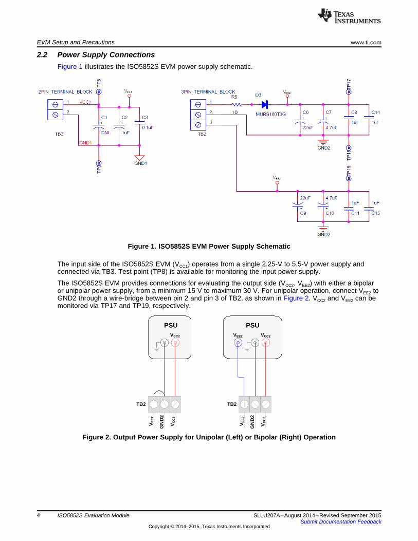
The ISO5852S EVM provides connections for evaluating the output side (VCC2, VEE2) with either a bipolaror unipolar power supply, from a minimum 15 V to maximum 30 V. For unipolar operation, connect VEE2 toGND2 through a wire-bridge between pin 2 and pin 3 of TB2, as shown in Figure 2. VCC2 and VEE2 can bemonitored via TP17 and TP19, respectively.
Figure 2. Output Power Supply for Unipolar (Left) or Bipolar (Right) Operation
4 ISO5852S Evaluation Module SLLU207A–August 2014–Revised September 2015Submit Documentation Feedback
2.3 Signal ConnectionsFigure 3 illustrates the ISO5852S EVM signal path schematic.
Figure 3. ISO5852S EVM Signal Path Schematic
2.3.1 I/O ConnectionsFigure 3 shows the signal path schematic of the EVM. JMP1 allows for stimulus or monitoring of thedevice I/O pins IN+, IN–, RDY, FLT, and RST. Test points 1, 2, 3, 4, and 5 provide additional access tothe I/O pins. The EVM comes populated with 10-kΩ pullup resistors (R1, R2) on the RDY and FLT pins,as well as 220-pF capacitors (C4, C5) to GND1 for noise filtering.
2.3.2 Output and LoadingThe EVM comes populated with a 1-nF load (C12) on the output side. The output can be monitoreddirectly via TP12. A 10:1 resistor-divider network is provided for monitoring the output with a low-voltageprobe via TP20. The divider circuit can be disconnected from the output by removing the shunt on JMP5.10-Ω gate resistors (R3, R4) control the rise and fall times of the output. These resistors can be modifiedby the user to alter the turn-on and turn-off characteristics of the output.
The EVM also allows for evaluation of the device with an IGBT load in either of the standard TO-247 orTO-220 footprints. During evaluation with an IGBT load, the pre-installed capacitive load (C12) can bedisconnected from the output by removing the shunt on JMP2.
The EVM provides an additional connection (P2) for applying an external power supply to the IGBTCollector. The EVM is not intended for high voltage testing and the voltage applied to P2 should be limitedto 50 V DC.
When evaluating the device with an IGBT load using P2, the components D1, D2, R7, and C13 should bepopulated with their default values, specified in Figure 3. Additionally, ensure that the DESAT pin is notconnected to GND2 when driving an IGBT load using P2, either by removing R8, or verifying that alljumpers are removed from JMP3.
5SLLU207A–August 2014–Revised September 2015 ISO5852S Evaluation ModuleSubmit Documentation Feedback
2.3.3 DESATThe EVM comes populated with a 220-pF DESAT capacitance. Pin1 on JMP3 can be used to apply asignal directly to the DESAT pin.
For evaluation with the default 1-nF load, when actual IGBT is not connected as load, the desaturationfunction should be disabled by connecting the DESAT pin to GND2 by shunting pin 1 to pin 2 on JMP3.
2.3.4 CLAMPBy default, the CLAMP pin is connected to the output via a 0-Ω resistor (R6). The CLAMP feature can bedisabled by removing R6. CLAMP can be monitored via TP14, and a signal can be applied directly to theCLAMP pin via JMP4.
3 Example MeasurementsFigure 4 illustrates measurements performed under the default EVM configuration. For thesemeasurements, VIN– is connected to GND1.
Figure 4. ISO5852S EVM Input and Output With Unipolar Output Supply
Figure 4 shows the input and output of the ISO5852S EVM for a 100-kHz clock with RG = 10 Ω (R3) andR4 = 10 Ω and a unipolar output supply (VCC2 = 15 V, VEE2 = GND2). The output is measured at TP12.
6 ISO5852S Evaluation Module SLLU207A–August 2014–Revised September 2015Submit Documentation Feedback
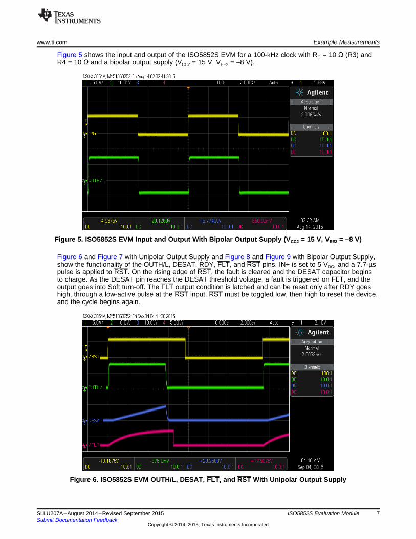
Figure 5 shows the input and output of the ISO5852S EVM for a 100-kHz clock with RG = 10 Ω (R3) andR4 = 10 Ω and a bipolar output supply (VCC2 = 15 V, VEE2 = –8 V).
Figure 5. ISO5852S EVM Input and Output With Bipolar Output Supply (VCC2 = 15 V, VEE2 = –8 V)
Figure 6 and Figure 7 with Unipolar Output Supply and Figure 8 and Figure 9 with Bipolar Output Supply,show the functionality of the OUTH/L, DESAT, RDY, FLT, and RST pins. IN+ is set to 5 VDC, and a 7.7-µspulse is applied to RST. On the rising edge of RST, the fault is cleared and the DESAT capacitor beginsto charge. As the DESAT pin reaches the DESAT threshold voltage, a fault is triggered on FLT, and theoutput goes into Soft turn-off. The FLT output condition is latched and can be reset only after RDY goeshigh, through a low-active pulse at the RST input. RST must be toggled low, then high to reset the device,and the cycle begins again.
Figure 6. ISO5852S EVM OUTH/L, DESAT, FLT, and RST With Unipolar Output Supply
7SLLU207A–August 2014–Revised September 2015 ISO5852S Evaluation ModuleSubmit Documentation Feedback
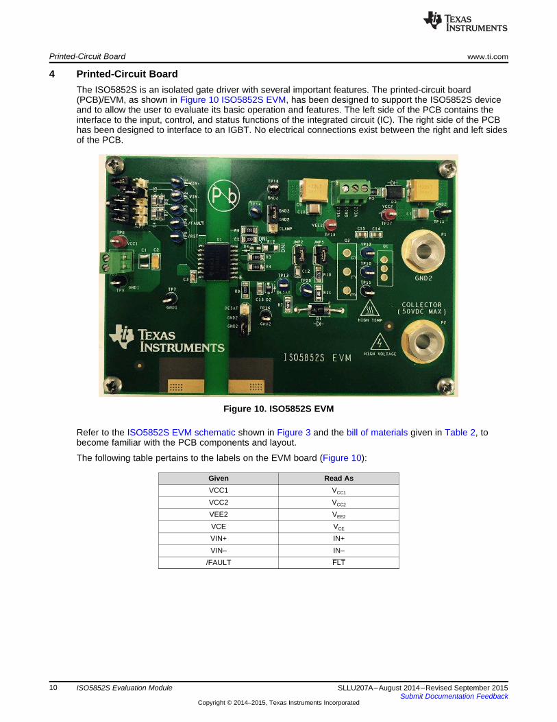
4 Printed-Circuit BoardThe ISO5852S is an isolated gate driver with several important features. The printed-circuit board(PCB)/EVM, as shown in Figure 10 ISO5852S EVM, has been designed to support the ISO5852S deviceand to allow the user to evaluate its basic operation and features. The left side of the PCB contains theinterface to the input, control, and status functions of the integrated circuit (IC). The right side of the PCBhas been designed to interface to an IGBT. No electrical connections exist between the right and left sidesof the PCB.
Figure 10. ISO5852S EVM
Refer to the ISO5852S EVM schematic shown in Figure 3 and the bill of materials given in Table 2, tobecome familiar with the PCB components and layout.
The following table pertains to the labels on the EVM board (Figure 10):
Given Read AsVCC1 VCC1
VCC2 VCC2
VEE2 VEE2
VCE VCE
VIN+ IN+VIN– IN–
/FAULT FLT
10 ISO5852S Evaluation Module SLLU207A–August 2014–Revised September 2015Submit Documentation Feedback
4.1.1 Left-Side Operation: DC Power, Control, and Status
4.1.1.1 DC Input PowerThe left side of the ISO5852S (and therefore the PCB) can be operated using either a 2.5-V (±10%) or 5-V(±10%) dc power supply. The user can choose to operate the ISO5852S EVM by battery. The dc powersupply must be connected to the TB3 terminal having VCC1 (+5.5 V DC) and GND1 (+5.5 V DC return).
4.1.1.2 Control and StatusThe interface to the device is via the JMP1 header. It contains the IN+ and IN– inputs, the device RST,RDY, and FLT indicator output. The JMP1 header allows easy connections to test equipment usingstandard clip leads. Each of the five signals also has a test point for additional connections. These are testpoints TP1–TP5.
4.1.2 Right-Side Operation
4.1.2.1 DC Output PowerPower is provided to VCC2 on the right side of the device at TB2 terminal as shown in Figure 2. The dcsupply must be able to provide a bias voltage over the range of +15 V DC to +30 V DC. The user canchoose to operate the ISO5852S EVM by battery. If a negative gate drive is required, a dc supply (orbattery) must be connected across VEE2 at the TB3 terminal as shown in Figure 2. The voltage range mustbe between 0 V and 15 V DC. The voltage across VCC2 and VEE2 must not exceed 30 V for operation.
4.1.2.2 DESAT – JMP3One of the features of the ISO5852S is the IGBT desaturation protection. JMP3 provides access to theDESAT pin. It is a 3-pin male header, and installing a shorting jumper between pin 1 and pin 2 on JMP3disables the DESAT function.
4.1.2.3 LoadAs shipped, the ISO5852S EVM does not have an IGBT installed. The user can evaluate device operationusing a capacitive load of 1 nF provided on EVM or capacitive load can be removed and IGBT can beconnected onto the board. Most IGBTs are available in the standard TO-247 or TO-220 package. ThePCB has provisions to solder an IGBT directly onto the board.
4.1.2.3.1 No IGBT Installed – JMP2When using the capacitive load, the user must install a jumper short onto JMP2. It connects a 1-nFcapacitor (C12) to the OUTH/L pin. The capacitive consists of the 10-Ω gate resistor (R3) and the 1-nFcapacitor (C12).
4.1.2.3.2 IGBT Installed – REMOVE JMP2If the user chooses to install an IGBT, JMP2 must be left open with no shorting jumper installed. The PCBhas been designed with plated-through holes (or vias) as Q1 and Q2 shown on the schematic for IGBTconnections.
11SLLU207A–August 2014–Revised September 2015 ISO5852S Evaluation ModuleSubmit Documentation Feedback
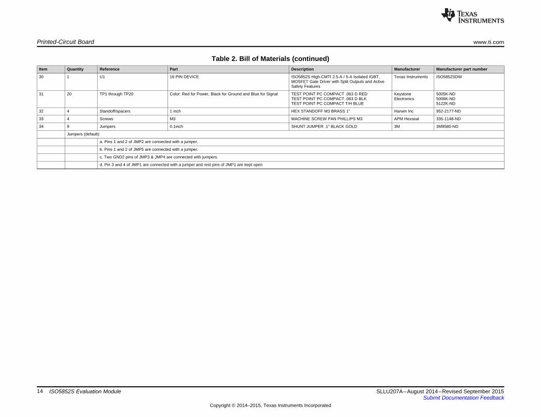
Table 2. Bill of Materials (continued)Item Quantity Reference Part Description Manufacturer Manufacturer part number
30 1 U1 16 PIN DEVICE ISO5852S High-CMTI 2.5-A / 5-A Isolated IGBT, Texas Instruments ISO5852SDWMOSFET Gate Driver with Split Outputs and ActiveSafety Features
31 20 TP1 through TP20 Color: Red for Power, Black for Ground and Blue for Signal TEST POINT PC COMPACT .063 D RED Keystone 5005K-NDTEST POINT PC COMPACT .063 D BLK Electronics 5006K-NDTEST POINT PC COMPACT T/H BLUE 5122K-ND
Changes from Original (August 2014) to A Revision ..................................................................................................... Page
• The entire manual has been changed for the A revision............................................................................. 1
NOTE: Page numbers for previous revisions may differ from page numbers in the current version.
15SLLU207A–August 2014–Revised September 2015 Revision HistorySubmit Documentation Feedback
STANDARD TERMS AND CONDITIONS FOR EVALUATION MODULES1. Delivery: TI delivers TI evaluation boards, kits, or modules, including any accompanying demonstration software, components, or
documentation (collectively, an “EVM” or “EVMs”) to the User (“User”) in accordance with the terms and conditions set forth herein.Acceptance of the EVM is expressly subject to the following terms and conditions.1.1 EVMs are intended solely for product or software developers for use in a research and development setting to facilitate feasibility
evaluation, experimentation, or scientific analysis of TI semiconductors products. EVMs have no direct function and are notfinished products. EVMs shall not be directly or indirectly assembled as a part or subassembly in any finished product. Forclarification, any software or software tools provided with the EVM (“Software”) shall not be subject to the terms and conditionsset forth herein but rather shall be subject to the applicable terms and conditions that accompany such Software
1.2 EVMs are not intended for consumer or household use. EVMs may not be sold, sublicensed, leased, rented, loaned, assigned,or otherwise distributed for commercial purposes by Users, in whole or in part, or used in any finished product or productionsystem.
2 Limited Warranty and Related Remedies/Disclaimers:2.1 These terms and conditions do not apply to Software. The warranty, if any, for Software is covered in the applicable Software
License Agreement.2.2 TI warrants that the TI EVM will conform to TI's published specifications for ninety (90) days after the date TI delivers such EVM
to User. Notwithstanding the foregoing, TI shall not be liable for any defects that are caused by neglect, misuse or mistreatmentby an entity other than TI, including improper installation or testing, or for any EVMs that have been altered or modified in anyway by an entity other than TI. Moreover, TI shall not be liable for any defects that result from User's design, specifications orinstructions for such EVMs. Testing and other quality control techniques are used to the extent TI deems necessary or asmandated by government requirements. TI does not test all parameters of each EVM.
2.3 If any EVM fails to conform to the warranty set forth above, TI's sole liability shall be at its option to repair or replace such EVM,or credit User's account for such EVM. TI's liability under this warranty shall be limited to EVMs that are returned during thewarranty period to the address designated by TI and that are determined by TI not to conform to such warranty. If TI elects torepair or replace such EVM, TI shall have a reasonable time to repair such EVM or provide replacements. Repaired EVMs shallbe warranted for the remainder of the original warranty period. Replaced EVMs shall be warranted for a new full ninety (90) daywarranty period.
3 Regulatory Notices:3.1 United States
3.1.1 Notice applicable to EVMs not FCC-Approved:This kit is designed to allow product developers to evaluate electronic components, circuitry, or software associated with the kitto determine whether to incorporate such items in a finished product and software developers to write software applications foruse with the end product. This kit is not a finished product and when assembled may not be resold or otherwise marketed unlessall required FCC equipment authorizations are first obtained. Operation is subject to the condition that this product not causeharmful interference to licensed radio stations and that this product accept harmful interference. Unless the assembled kit isdesigned to operate under part 15, part 18 or part 95 of this chapter, the operator of the kit must operate under the authority ofan FCC license holder or must secure an experimental authorization under part 5 of this chapter.3.1.2 For EVMs annotated as FCC – FEDERAL COMMUNICATIONS COMMISSION Part 15 Compliant:
CAUTIONThis device complies with part 15 of the FCC Rules. Operation is subject to the following two conditions: (1) This device may notcause harmful interference, and (2) this device must accept any interference received, including interference that may causeundesired operation.Changes or modifications not expressly approved by the party responsible for compliance could void the user's authority tooperate the equipment.
FCC Interference Statement for Class A EVM devicesNOTE: This equipment has been tested and found to comply with the limits for a Class A digital device, pursuant to part 15 ofthe FCC Rules. These limits are designed to provide reasonable protection against harmful interference when the equipment isoperated in a commercial environment. This equipment generates, uses, and can radiate radio frequency energy and, if notinstalled and used in accordance with the instruction manual, may cause harmful interference to radio communications.Operation of this equipment in a residential area is likely to cause harmful interference in which case the user will be required tocorrect the interference at his own expense.
SPACER
SPACER
SPACER
SPACER
SPACER
SPACER
SPACER
SPACER
FCC Interference Statement for Class B EVM devicesNOTE: This equipment has been tested and found to comply with the limits for a Class B digital device, pursuant to part 15 ofthe FCC Rules. These limits are designed to provide reasonable protection against harmful interference in a residentialinstallation. This equipment generates, uses and can radiate radio frequency energy and, if not installed and used in accordancewith the instructions, may cause harmful interference to radio communications. However, there is no guarantee that interferencewill not occur in a particular installation. If this equipment does cause harmful interference to radio or television reception, whichcan be determined by turning the equipment off and on, the user is encouraged to try to correct the interference by one or moreof the following measures:
• Reorient or relocate the receiving antenna.• Increase the separation between the equipment and receiver.• Connect the equipment into an outlet on a circuit different from that to which the receiver is connected.• Consult the dealer or an experienced radio/TV technician for help.
3.2 Canada3.2.1 For EVMs issued with an Industry Canada Certificate of Conformance to RSS-210
Concerning EVMs Including Radio Transmitters:This device complies with Industry Canada license-exempt RSS standard(s). Operation is subject to the following two conditions:(1) this device may not cause interference, and (2) this device must accept any interference, including interference that maycause undesired operation of the device.
Concernant les EVMs avec appareils radio:Le présent appareil est conforme aux CNR d'Industrie Canada applicables aux appareils radio exempts de licence. L'exploitationest autorisée aux deux conditions suivantes: (1) l'appareil ne doit pas produire de brouillage, et (2) l'utilisateur de l'appareil doitaccepter tout brouillage radioélectrique subi, même si le brouillage est susceptible d'en compromettre le fonctionnement.
Concerning EVMs Including Detachable Antennas:Under Industry Canada regulations, this radio transmitter may only operate using an antenna of a type and maximum (or lesser)gain approved for the transmitter by Industry Canada. To reduce potential radio interference to other users, the antenna typeand its gain should be so chosen that the equivalent isotropically radiated power (e.i.r.p.) is not more than that necessary forsuccessful communication. This radio transmitter has been approved by Industry Canada to operate with the antenna typeslisted in the user guide with the maximum permissible gain and required antenna impedance for each antenna type indicated.Antenna types not included in this list, having a gain greater than the maximum gain indicated for that type, are strictly prohibitedfor use with this device.
Concernant les EVMs avec antennes détachablesConformément à la réglementation d'Industrie Canada, le présent émetteur radio peut fonctionner avec une antenne d'un type etd'un gain maximal (ou inférieur) approuvé pour l'émetteur par Industrie Canada. Dans le but de réduire les risques de brouillageradioélectrique à l'intention des autres utilisateurs, il faut choisir le type d'antenne et son gain de sorte que la puissance isotroperayonnée équivalente (p.i.r.e.) ne dépasse pas l'intensité nécessaire à l'établissement d'une communication satisfaisante. Leprésent émetteur radio a été approuvé par Industrie Canada pour fonctionner avec les types d'antenne énumérés dans lemanuel d’usage et ayant un gain admissible maximal et l'impédance requise pour chaque type d'antenne. Les types d'antennenon inclus dans cette liste, ou dont le gain est supérieur au gain maximal indiqué, sont strictement interdits pour l'exploitation del'émetteur
3.3 Japan3.3.1 Notice for EVMs delivered in Japan: Please see http://www.tij.co.jp/lsds/ti_ja/general/eStore/notice_01.page 日本国内に
3.3.2 Notice for Users of EVMs Considered “Radio Frequency Products” in Japan: EVMs entering Japan are NOT certified byTI as conforming to Technical Regulations of Radio Law of Japan.
If User uses EVMs in Japan, User is required by Radio Law of Japan to follow the instructions below with respect to EVMs:1. Use EVMs in a shielded room or any other test facility as defined in the notification #173 issued by Ministry of Internal
Affairs and Communications on March 28, 2006, based on Sub-section 1.1 of Article 6 of the Ministry’s Rule forEnforcement of Radio Law of Japan,
2. Use EVMs only after User obtains the license of Test Radio Station as provided in Radio Law of Japan with respect toEVMs, or
3. Use of EVMs only after User obtains the Technical Regulations Conformity Certification as provided in Radio Law of Japanwith respect to EVMs. Also, do not transfer EVMs, unless User gives the same notice above to the transferee. Please notethat if User does not follow the instructions above, User will be subject to penalties of Radio Law of Japan.
3.3.3 Notice for EVMs for Power Line Communication: Please see http://www.tij.co.jp/lsds/ti_ja/general/eStore/notice_02.page電力線搬送波通信についての開発キットをお使いになる際の注意事項については、次のところをご覧ください。http://www.tij.co.jp/lsds/ti_ja/general/eStore/notice_02.page
SPACER4 EVM Use Restrictions and Warnings:
4.1 EVMS ARE NOT FOR USE IN FUNCTIONAL SAFETY AND/OR SAFETY CRITICAL EVALUATIONS, INCLUDING BUT NOTLIMITED TO EVALUATIONS OF LIFE SUPPORT APPLICATIONS.
4.2 User must read and apply the user guide and other available documentation provided by TI regarding the EVM prior to handlingor using the EVM, including without limitation any warning or restriction notices. The notices contain important safety informationrelated to, for example, temperatures and voltages.
4.3 Safety-Related Warnings and Restrictions:4.3.1 User shall operate the EVM within TI’s recommended specifications and environmental considerations stated in the user
guide, other available documentation provided by TI, and any other applicable requirements and employ reasonable andcustomary safeguards. Exceeding the specified performance ratings and specifications (including but not limited to inputand output voltage, current, power, and environmental ranges) for the EVM may cause personal injury or death, orproperty damage. If there are questions concerning performance ratings and specifications, User should contact a TIfield representative prior to connecting interface electronics including input power and intended loads. Any loads appliedoutside of the specified output range may also result in unintended and/or inaccurate operation and/or possiblepermanent damage to the EVM and/or interface electronics. Please consult the EVM user guide prior to connecting anyload to the EVM output. If there is uncertainty as to the load specification, please contact a TI field representative.During normal operation, even with the inputs and outputs kept within the specified allowable ranges, some circuitcomponents may have elevated case temperatures. These components include but are not limited to linear regulators,switching transistors, pass transistors, current sense resistors, and heat sinks, which can be identified using theinformation in the associated documentation. When working with the EVM, please be aware that the EVM may becomevery warm.
4.3.2 EVMs are intended solely for use by technically qualified, professional electronics experts who are familiar with thedangers and application risks associated with handling electrical mechanical components, systems, and subsystems.User assumes all responsibility and liability for proper and safe handling and use of the EVM by User or its employees,affiliates, contractors or designees. User assumes all responsibility and liability to ensure that any interfaces (electronicand/or mechanical) between the EVM and any human body are designed with suitable isolation and means to safelylimit accessible leakage currents to minimize the risk of electrical shock hazard. User assumes all responsibility andliability for any improper or unsafe handling or use of the EVM by User or its employees, affiliates, contractors ordesignees.
4.4 User assumes all responsibility and liability to determine whether the EVM is subject to any applicable international, federal,state, or local laws and regulations related to User’s handling and use of the EVM and, if applicable, User assumes allresponsibility and liability for compliance in all respects with such laws and regulations. User assumes all responsibility andliability for proper disposal and recycling of the EVM consistent with all applicable international, federal, state, and localrequirements.
5. Accuracy of Information: To the extent TI provides information on the availability and function of EVMs, TI attempts to be as accurateas possible. However, TI does not warrant the accuracy of EVM descriptions, EVM availability or other information on its websites asaccurate, complete, reliable, current, or error-free.
6.1 EXCEPT AS SET FORTH ABOVE, EVMS AND ANY WRITTEN DESIGN MATERIALS PROVIDED WITH THE EVM (AND THEDESIGN OF THE EVM ITSELF) ARE PROVIDED "AS IS" AND "WITH ALL FAULTS." TI DISCLAIMS ALL OTHERWARRANTIES, EXPRESS OR IMPLIED, REGARDING SUCH ITEMS, INCLUDING BUT NOT LIMITED TO ANY IMPLIEDWARRANTIES OF MERCHANTABILITY OR FITNESS FOR A PARTICULAR PURPOSE OR NON-INFRINGEMENT OF ANYTHIRD PARTY PATENTS, COPYRIGHTS, TRADE SECRETS OR OTHER INTELLECTUAL PROPERTY RIGHTS.
6.2 EXCEPT FOR THE LIMITED RIGHT TO USE THE EVM SET FORTH HEREIN, NOTHING IN THESE TERMS ANDCONDITIONS SHALL BE CONSTRUED AS GRANTING OR CONFERRING ANY RIGHTS BY LICENSE, PATENT, OR ANYOTHER INDUSTRIAL OR INTELLECTUAL PROPERTY RIGHT OF TI, ITS SUPPLIERS/LICENSORS OR ANY OTHER THIRDPARTY, TO USE THE EVM IN ANY FINISHED END-USER OR READY-TO-USE FINAL PRODUCT, OR FOR ANYINVENTION, DISCOVERY OR IMPROVEMENT MADE, CONCEIVED OR ACQUIRED PRIOR TO OR AFTER DELIVERY OFTHE EVM.
7. USER'S INDEMNITY OBLIGATIONS AND REPRESENTATIONS. USER WILL DEFEND, INDEMNIFY AND HOLD TI, ITSLICENSORS AND THEIR REPRESENTATIVES HARMLESS FROM AND AGAINST ANY AND ALL CLAIMS, DAMAGES, LOSSES,EXPENSES, COSTS AND LIABILITIES (COLLECTIVELY, "CLAIMS") ARISING OUT OF OR IN CONNECTION WITH ANYHANDLING OR USE OF THE EVM THAT IS NOT IN ACCORDANCE WITH THESE TERMS AND CONDITIONS. THIS OBLIGATIONSHALL APPLY WHETHER CLAIMS ARISE UNDER STATUTE, REGULATION, OR THE LAW OF TORT, CONTRACT OR ANYOTHER LEGAL THEORY, AND EVEN IF THE EVM FAILS TO PERFORM AS DESCRIBED OR EXPECTED.
8. Limitations on Damages and Liability:8.1 General Limitations. IN NO EVENT SHALL TI BE LIABLE FOR ANY SPECIAL, COLLATERAL, INDIRECT, PUNITIVE,
INCIDENTAL, CONSEQUENTIAL, OR EXEMPLARY DAMAGES IN CONNECTION WITH OR ARISING OUT OF THESETERMS ANDCONDITIONS OR THE USE OF THE EVMS PROVIDED HEREUNDER, REGARDLESS OF WHETHER TI HASBEEN ADVISED OF THE POSSIBILITY OF SUCH DAMAGES. EXCLUDED DAMAGES INCLUDE, BUT ARE NOT LIMITEDTO, COST OF REMOVAL OR REINSTALLATION, ANCILLARY COSTS TO THE PROCUREMENT OF SUBSTITUTE GOODSOR SERVICES, RETESTING, OUTSIDE COMPUTER TIME, LABOR COSTS, LOSS OF GOODWILL, LOSS OF PROFITS,LOSS OF SAVINGS, LOSS OF USE, LOSS OF DATA, OR BUSINESS INTERRUPTION. NO CLAIM, SUIT OR ACTION SHALLBE BROUGHT AGAINST TI MORE THAN ONE YEAR AFTER THE RELATED CAUSE OF ACTION HAS OCCURRED.
8.2 Specific Limitations. IN NO EVENT SHALL TI'S AGGREGATE LIABILITY FROM ANY WARRANTY OR OTHER OBLIGATIONARISING OUT OF OR IN CONNECTION WITH THESE TERMS AND CONDITIONS, OR ANY USE OF ANY TI EVMPROVIDED HEREUNDER, EXCEED THE TOTAL AMOUNT PAID TO TI FOR THE PARTICULAR UNITS SOLD UNDERTHESE TERMS AND CONDITIONS WITH RESPECT TO WHICH LOSSES OR DAMAGES ARE CLAIMED. THE EXISTENCEOF MORE THAN ONE CLAIM AGAINST THE PARTICULAR UNITS SOLD TO USER UNDER THESE TERMS ANDCONDITIONS SHALL NOT ENLARGE OR EXTEND THIS LIMIT.
9. Return Policy. Except as otherwise provided, TI does not offer any refunds, returns, or exchanges. Furthermore, no return of EVM(s)will be accepted if the package has been opened and no return of the EVM(s) will be accepted if they are damaged or otherwise not ina resalable condition. If User feels it has been incorrectly charged for the EVM(s) it ordered or that delivery violates the applicableorder, User should contact TI. All refunds will be made in full within thirty (30) working days from the return of the components(s),excluding any postage or packaging costs.
10. Governing Law: These terms and conditions shall be governed by and interpreted in accordance with the laws of the State of Texas,without reference to conflict-of-laws principles. User agrees that non-exclusive jurisdiction for any dispute arising out of or relating tothese terms and conditions lies within courts located in the State of Texas and consents to venue in Dallas County, Texas.Notwithstanding the foregoing, any judgment may be enforced in any United States or foreign court, and TI may seek injunctive reliefin any United States or foreign court.
Texas Instruments Incorporated and its subsidiaries (TI) reserve the right to make corrections, enhancements, improvements and otherchanges to its semiconductor products and services per JESD46, latest issue, and to discontinue any product or service per JESD48, latestissue. Buyers should obtain the latest relevant information before placing orders and should verify that such information is current andcomplete. All semiconductor products (also referred to herein as “components”) are sold subject to TI’s terms and conditions of salesupplied at the time of order acknowledgment.TI warrants performance of its components to the specifications applicable at the time of sale, in accordance with the warranty in TI’s termsand conditions of sale of semiconductor products. Testing and other quality control techniques are used to the extent TI deems necessaryto support this warranty. Except where mandated by applicable law, testing of all parameters of each component is not necessarilyperformed.TI assumes no liability for applications assistance or the design of Buyers’ products. Buyers are responsible for their products andapplications using TI components. To minimize the risks associated with Buyers’ products and applications, Buyers should provideadequate design and operating safeguards.TI does not warrant or represent that any license, either express or implied, is granted under any patent right, copyright, mask work right, orother intellectual property right relating to any combination, machine, or process in which TI components or services are used. Informationpublished by TI regarding third-party products or services does not constitute a license to use such products or services or a warranty orendorsement thereof. Use of such information may require a license from a third party under the patents or other intellectual property of thethird party, or a license from TI under the patents or other intellectual property of TI.Reproduction of significant portions of TI information in TI data books or data sheets is permissible only if reproduction is without alterationand is accompanied by all associated warranties, conditions, limitations, and notices. TI is not responsible or liable for such altereddocumentation. Information of third parties may be subject to additional restrictions.Resale of TI components or services with statements different from or beyond the parameters stated by TI for that component or servicevoids all express and any implied warranties for the associated TI component or service and is an unfair and deceptive business practice.TI is not responsible or liable for any such statements.Buyer acknowledges and agrees that it is solely responsible for compliance with all legal, regulatory and safety-related requirementsconcerning its products, and any use of TI components in its applications, notwithstanding any applications-related information or supportthat may be provided by TI. Buyer represents and agrees that it has all the necessary expertise to create and implement safeguards whichanticipate dangerous consequences of failures, monitor failures and their consequences, lessen the likelihood of failures that might causeharm and take appropriate remedial actions. Buyer will fully indemnify TI and its representatives against any damages arising out of the useof any TI components in safety-critical applications.In some cases, TI components may be promoted specifically to facilitate safety-related applications. With such components, TI’s goal is tohelp enable customers to design and create their own end-product solutions that meet applicable functional safety standards andrequirements. Nonetheless, such components are subject to these terms.No TI components are authorized for use in FDA Class III (or similar life-critical medical equipment) unless authorized officers of the partieshave executed a special agreement specifically governing such use.Only those TI components which TI has specifically designated as military grade or “enhanced plastic” are designed and intended for use inmilitary/aerospace applications or environments. Buyer acknowledges and agrees that any military or aerospace use of TI componentswhich have not been so designated is solely at the Buyer's risk, and that Buyer is solely responsible for compliance with all legal andregulatory requirements in connection with such use.TI has specifically designated certain components as meeting ISO/TS16949 requirements, mainly for automotive use. In any case of use ofnon-designated products, TI will not be responsible for any failure to meet ISO/TS16949.
Products ApplicationsAudio www.ti.com/audio Automotive and Transportation www.ti.com/automotiveAmplifiers amplifier.ti.com Communications and Telecom www.ti.com/communicationsData Converters dataconverter.ti.com Computers and Peripherals www.ti.com/computersDLP® Products www.dlp.com Consumer Electronics www.ti.com/consumer-appsDSP dsp.ti.com Energy and Lighting www.ti.com/energyClocks and Timers www.ti.com/clocks Industrial www.ti.com/industrialInterface interface.ti.com Medical www.ti.com/medicalLogic logic.ti.com Security www.ti.com/securityPower Mgmt power.ti.com Space, Avionics and Defense www.ti.com/space-avionics-defenseMicrocontrollers microcontroller.ti.com Video and Imaging www.ti.com/videoRFID www.ti-rfid.comOMAP Applications Processors www.ti.com/omap TI E2E Community e2e.ti.comWireless Connectivity www.ti.com/wirelessconnectivity