An IMPORTANT NOTICE at the end of this data sheet addresses availability, warranty, changes, use in safety-critical applications,intellectual property matters and other important disclaimers. PRODUCTION DATA.
ISO7821LLSSLLSET5A –MARCH 2016–REVISED SEPTEMBER 2016
1 Features1• Complies with TIA/EIA-644-A LVDS Standard• Signaling Rate: 50 Mbps to 150 Mbps• Optimized for DC-Balanced Data• Wide Supply Range: 3 V to 5.5 V• Wide Temperature Range: –55°C to 125°C• Low-Power Consumption, Typical 10.3 mA per
Channel at 150 Mbps• Low Propagation Delay: 17 ns Typical• Industry leading CMTI(Min): ±100 kV/μs• Robust Electromagnetic Compatibility (EMC)• System-Level ESD, EFT, and Surge Immunity• Low Emissions• Isolation Barrier Life: > 40 Years• SOIC-16 Wide Body (DW) and Extra-Wide Body
(DWW) Package Options• Isolation Surge Withstand Voltage 12800 VPK
• Safety-Related Certifications:– 8000-VPK Reinforced Isolation per DIN V VDE
V 0884–10 (VDE V 0884–10): 2006–12– 5700-VRMS Isolation for 1 minute per UL 1577– CSA Component Acceptance Notice 5A, IEC
60950–1 and IEC 60601–1 End EquipmentStandards
– TUV Certification per EN 61010-1 and EN60950-1
– CQC Certification per GB4943.1–2011– All Certifications are Planned
2 Applications• Motor Control• Test and Measurement• Industrial Automation• Medical Equipment• Communication Systems
3 DescriptionThe ISO7821LLS device is a high-performance,isolated dual-LVDS buffer with 8000-VPK isolationvoltage. This device provides high electromagneticimmunity and low emissions at low-powerconsumption, while isolating the LVDS bus signal.Each isolation channel has an LVDS receive andtransmit buffer. Timing performance for theISO7821LLS device is optimized for use withcommunication systems that use DC-balanced datastreams which is achieved through an internaldistortion correction scheme.
The ISO7821LLS device has one forward and onereverse-direction channel.
Through innovative chip design and layouttechniques, the electromagnetic compatibility of theISO7821LLS device has been significantly enhancedto ease system-level ESD, EFT, surge, andemissions compliance.
The ISO7821LLS device is available in a 16-pin SOICwide-body (DW) and extra-wide body (DWW)packages.
Device Information(1)
PART NUMBER PACKAGE BODY SIZE (NOM)
ISO7821LLSDW (16) 10.30 mm × 7.50 mmDWW (16) 10.30 mm × 14.00 mm
(1) For all available packages, see the orderable addendum atthe end of the data sheet.
Simplified Schematic
VCCI and GNDI are supply and ground connections respectively for the input channels.VCCO and GNDO are supply and ground connections respectively for the output channels.
(1) Stresses beyond those listed under Absolute Maximum Ratings may cause permanent damage to the device. These are stress ratingsonly, which do not imply functional operation of the device at these or any other conditions beyond those indicated under RecommendedOperating Conditions. Exposure to absolute-maximum-rated conditions for extended periods may affect device reliability.
(2) All voltage values except differential I/O bus voltages are with respect to the local ground pin (GND1 or GND2) and are peak voltagevalues.
(3) Maximum voltage must not exceed 6 V.
6 Specifications
6.1 Absolute Maximum Ratingsover operating free-air temperature range (unless otherwise noted) (1)
MIN MAX UNITVCCx Supply voltage (2) VCC1, VCC2 –0.5 6 V
V Voltage on input, output, andenable pins OUTx, INx, ENx –0.5 VCCx + 0.5 (3) V
IO Maximum current through OUTx pins –20 20 mATJ Junction temperature –55 150 °CTstg Storage temperature –65 150 °C
(1) JEDEC document JEP155 states that 500-V HBM allows safe manufacturing with a standard ESD control process.(2) JEDEC document JEP157 states that 250-V CDM allows safe manufacturing with a standard ESD control process.
6.2 ESD RatingsVALUE UNIT
V(ESD)Electrostaticdischarge
Human-body model (HBM), per ANSI/ESDA/JEDEC JS-001 (1) ±4500V
Charged-device model (CDM), per JEDEC specification JESD22-C101 (2) ±1500
6.3 Recommended Operating ConditionsMIN NOM MAX UNIT
VCC1, VCC2 Supply voltage 3 3.3 5.5 V
|VID| Magnitude of RX inputdifferential voltage Driven with voltage sources on RX pins 100 600 mV
VICRX input common-mode voltage VCC1, VCC2 ≥ 3 V 0.5 |VID| 2.4 – 0.5 |VID| V
RL TX far-end differential termination 100 Ω
DR Signaling rate 50 150 MbpsTA Ambient temperature –55 25 125 °C
PARAMETER TEST CONDITIONS MAX TYP MAX UNITPD Maximum power dissipation (both sides) 180 mWPD1 Maximum power dissipation (side 1) 90 mWPD2 Maximum power dissipation (side 2) 90 mW
(1) Creepage and clearance requirements should be applied according to the specific equipment isolation standards of an application. Careshould be taken to maintain the creepage and clearance distance of a board design to ensure that the mounting pads of the isolator onthe printed-circuit board do not reduce this distance. Creepage and clearance on a printed-circuit board become equal in certain cases.Techniques such as inserting grooves and/or ribs on a printed circuit board are used to help increase these specifications.
(2) This coupler is suitable for safe electrical insulation only within the safety ratings. Compliance with the safety ratings shall be ensured bymeans of suitable protective circuits.
(3) Testing is carried out in air or oil to determine the intrinsic surge immunity of the isolation barrier.(4) Apparent charge is electrical discharge caused by a partial discharge (pd).(5) All pins on each side of the barrier tied together creating a two-terminal device.
6.6 Insulation Specificationsover operating free-air temperature range (unless otherwise noted)
PARAMETER TEST CONDITIONSSPECIFICATION
UNITDW DWW
GENERALCLR External clearance (1) Shortest terminal-to-terminal distance through air >8 >14.5 mm
CPG External creepage (1) Shortest terminal-to-terminal distance across thepackage surface >8 >14.5 mm
DTI Distance through the insulation Minimum internal gap (internal clearance) >21 >21 μm
CTI Tracking resistance (comparativetracking index) DIN EN 60112 (VDE 0303–11); IEC 60112; UL 746A >600 >600 V
Material group According to IEC 60664-1 I I
Overvoltage category per IEC 60664-1Rated mains voltage ≤ 600 VRMS I–IV I–IVRated mains voltage ≤ 1000 VRMS I–III I–IV
DIN V VDE V 0884–10 (VDE V 0884–10):2006–12 (2)
VIORMMaximum repetitive peak isolationvoltage AC voltage (bipolar) 2121 2828 VPK
VIOWM Maximum isolation working voltageAC voltage (sine wave); time dependent dielectricbreakdown (TDDB) test; see Figure 1 and Figure 2 1500 2000 VRMS
DC voltage 2121 2828 VDC
VIOTM Maximum transient isolation voltage VTEST = VIOTM, t = 60 s (qualification)t = 1 s (100% production) 8000 8000 VPK
VIOSM Maximum surge isolation voltage (3) Test method per IEC 60065, 1.2/50 µs waveform,VTEST = 1.6 × VIOSM = 12800 VPK (qualification) 8000 8000 VPK
qpd Apparent charge (4)
Method a: After I/O safety test subgroup 2/3,Vini = VIOTM, tini = 60 s;Vpd(m) = 1.2 × VIORM = 2545 VPK (DW) and3394 VPK (DWW), tm = 10 s
≤5 ≤5
pC
Method a: After environmental tests subgroup 1,Vini = VIOTM, tini = 60 s;Vpd(m) = 1.6 × VIORM = 3394 VPK (DW) and4525 VPK (DWW), tm = 10 s
≤5 ≤5
Method b1: At routine test (100% production) andpreconditioning (type test)Vini = VIORM, tini = 1 s;Vpd(m) = 1.875 × VIORM= 3977 VPK (DW) and5303 VPK (DWW), tm = 1 s
≤5 ≤5
CIO Barrier capacitance, input to output (5) VIO = 0.4 × sin (2πft), f = 1 MHz ~0.7 ~0.7 pF
Reinforced insulation per CSA60950-1-07+A1+A2 and IEC60950-1 2nd Ed., 800 VRMS(DW package) and 1450 VRMS(DWW package) max workingvoltage (pollution degree 2,material group I);
Single protection,5700 VRMS
Reinforced Insulation,Altitude ≤ 5000 m, TropicalClimate, 250 VRMSmaximum working voltage
5700 VRMS Reinforced insulation perEN 61010-1:2010 (3rd Ed) up toworking voltage of 600 VRMS (DWpackage) and 1000 VRMS (DWWpackage)
2 MOPP (Means of PatientProtection) per CSA 60601-1:14 and IEC 60601-1 Ed. 3.1,250 VRMS (354 VPK) maxworking voltage (DW package)
5700 VRMS Reinforced insulation perEN 60950-1:2006/A11:2009/A1:2010/A12:2011/A2:2013 up to workingvoltage of 800 VRMS (DW package) and1450 VRMS (DWW package)
6.8 Safety Limiting ValuesSafety limiting intends to minimize potential damage to the isolation barrier upon failure of input or output circuitry. A failure ofthe I/O can allow low resistance to ground or the supply and, without current limiting, dissipate sufficient power to overheatthe die and damage the isolation barrier potentially leading to secondary system failures.
PARAMETER TEST CONDITIONS MIN TYP MAX UNITDW PACKAGE
ISSafety input, output, or supplycurrent
RθJA = 82°C/W, VI = 5.5 V, TJ = 150°C, TA = 25°C,see Figure 3 277
mARθJA = 82°C/W, VI = 3.6 V, TJ = 150°C, TA = 25°C,see Figure 3 423
PS Safety input, output, or total power RθJA = 82°C/W, TJ = 150°C, TA = 25°C,see Figure 5 1524 mW
TS Maximum safety temperature 150 °CDWW PACKAGE
ISSafety input, output, or supplycurrent
RθJA = 84.6°C/W, VI = 5.5 V, TJ = 150°C, TA = 25°C,see Figure 4 269
mARθJA = 84.6°C/W, VI = 3.6 V, TJ = 150°C, TA = 25°C,see Figure 4 410
PS Safety input, output, or total power RθJA = 84.6°C/W, TJ = 150°C, TA = 25°C,see Figure 6 1478 mW
TS Maximum safety temperature 150 °C
The maximum safety temperature is the maximum junction temperature specified for the device. The powerdissipation and junction-to-air thermal impedance of the device installed in the application hardware determinesthe junction temperature. The assumed junction-to-air thermal resistance in the Thermal Information is that of adevice installed on a High-K test board for leaded surface-mount packages. The power is the recommendedmaximum input voltage times the current. The junction temperature is then the ambient temperature plus thepower times the junction-to-air thermal resistance.
EN1 = EN2 = 1, RL = 100-Ω differential, data communication at125 Mbps 9.7 15.5
EN1 = EN2 = 1, RL = 100-Ω differential, data communication at150 Mbps 10.3 16.4
6.11 Timing Requirements for Distortion Correction SchemeValid data = 8b10b like data with DC balance and bounded disparity. See Figure 25.
MIN NOM MAX UNIT
tCALIB
Time to complete internal calibration, after exiting idle state. LVDS TXoutput is held high during this time. During this time valid data must bepresented at the receiver.
250 750 µs
tIDLEThe minimum duration of any idle state that must be maintained betweenvalid data transmissions. 10 µs
tIDLE_OUTAfter a channel enters idle state, the internal calibration loses lock after thistime, and the LVDS outputs are gated high. 200 600 ns
8.1 OverviewThe ISO7821LLS device is an isolated LVDS buffer. The differential signal received on the LVDS input pins isfirst converted to CMOS logic levels. It is then transmitted across a silicon dioxide based capacitive isolationbarrier using an On-Off Keying (OOK) modulation scheme. A high frequency carrier transmitted across thebarrier represents one logic state and an absence of a carrier represents the other logic state. On the other sideof the barrier a demodulator converts the OOK signal back to logic levels, which is then converted to LVDSoutputs by a differential driver. This device incorporates advanced circuit techniques to maximize CMTIperformance and minimize radiated emissions.
The ISO7821LLS device implements an eye-diagram improvement scheme to correct for signal distortions thatare introduced in the LVDS receiver as well as the isolation channel. This enables the device to guarantee aneye closure of less than 30% at 125 Mbps, and less than 40% at 150 Mbps. The distortion correction scheme isoptimized for operation with DC balanced data (for example 8b10b or equivalent) with a maximum run length of6. The minimum data-rate of operation is also constrained to 50 Mbps. For general purpose data communicationfrom 0 to 100 Mbps, the ISO782xLL family of devices should be considered.
The ISO7821LLS device is TIA/EIA-644-A standard compliant. The LVDS transmitter drives a minimumdifferential-output voltage magnitude of 250 mV into a 100-Ω load, and the LVDS receiver is capable of detectingdifferential signal ≥50 mV in magnitude. The device consumes 11 mA per channel at 150 Mbps with 5-Vsupplies.
The Functional Block Diagram section shows a conceptual block diagram of one channel of the ISO7821LLSdevice.
(1) See the Safety-Related Certifications section for detailed isolation ratings.
8.3 Feature DescriptionThe ISO7821LLS device is available in a two-channel configuration with a default differential-high output state.Table 1 lists the device features.
Table 1. Device FeaturesPART
NUMBER CHANNEL DIRECTION RATED ISOLATION MAXIMUM DATA RATE DEFAULT DIFFERENTIALOUTPUT
8.3.1 Distortion-Correction SchemeThe ISO7821LLS device implements a distortion-correction scheme to correct for signal distortions that areintroduced in the LVDS receiver as well as the isolation channel. This scheme is optimized for a DC-balanceddata-stream with a maximum run length of 6. One example of such a data stream is 8b10b encoded data. Theminimum data rate supported by the ISO7821LLS device is 50 Mbps and the maximum is 150 Mbps.
Figure 25 shows the timing requirements associated with the distortion correction scheme (see the TimingRequirements for Distortion Correction Scheme table for timing parameters). The input to the LVDS channelshould be either idle low, idle high, or should have clock or DC-balanced data transitions at 25 MHz / 50 Mbps orhigher. Low frequency or DC-unbalanced data is not allowed. The distortion-correction scheme runs an internalcalibration each time the LVDS channel transitions from an idle state to a data transmission state. The calibrationruns for a period of tCALIB during which the LVDS channel output is held at logic high. This calibration is also runat power up. Lack of activity on the receive inputs for a period greater than tIDLE_OUT takes the channel to anuncalibrated state. If the communication protocol requires the channel to transition to the idle state, the idle-highor idle-low state must be held for at least duration of tIDLE.
A. Signals shown are differential logic states.Logic high → VIN+ > VIN–Logic low → VIN– > VIN+
B. The data to ISOLVDS channel should be either idle high, idle low, clock, or valid data.Valid data = 8b10b like data with DC balance and bounded disparity.
C. When transitioning from an uncalibrated sate to a calibrated state, the ISOLVDS channel output is gated high for upto tCALIB, during which the channel is calibrated.
D. If the channel finds no transitions in the incoming data for a period of tIDLE_OUT, the channel goes to an uncalibratedstate.
E. Power loss (which implies no data transitions) takes the channel to an uncalibrated state.F. If, for some reason, the idle-high or idle-low state must be held on the line, this state must be held for at least tIDLE.
(1) VCCI = Input-side VCC; VCCO = Output-side VCC; PU = Powered up (VCCx ≥ 2.25 V); PD = Powered down (VCCx ≤ 1.7 V); X = Irrelevant(2) Input (INx±): H = high level (VID ≥ 50 mV); L = low level (VID ≤ –50 mV); I = indeterminate (–50 mV < VID < 50 mV)(3) Output (OUTx±): H = high level (VOD ≥ 250 mV); L = low level (VOD ≤ –250 mV); Z = high impedance.
8.4 Device Functional ModesTable 2 lists the functional modes for the ISO7821LLS device.
Table 2. ISO7821LLS Function Table (1)
VCCI VCCOINPUT
(INx±) (2)OUTPUT ENABLE
(ENx)OUTPUT
(OUTx±) (3) COMMENTS
PU PU
H H or open H Normal Operation:A channel output assumes the logic state of the input.L H or open L
I H or open H or L
X PU X L Z A low-logic state at the output enable causes the outputs to be in highimpedance.
PD PU X H or open H
Default mode: When VCCI is unpowered, a channel output assumesthe logic high state.When VCCI transitions from unpowered to powered up, a channeloutput assumes the logic state of the input.When VCCI transitions from powered up to unpowered, a channeloutput assumes the selected default high state.
X PD X X UndeterminedWhen VCCO is unpowered, a channel output is undetermined.When VCCO transitions from unpowered to powered up, a channeloutput assumes the logic state of the input
NOTEInformation in the following applications sections is not part of the TI componentspecification, and TI does not warrant its accuracy or completeness. TI’s customers areresponsible for determining suitability of components for their purposes. Customers shouldvalidate and test their design implementation to confirm system functionality.
9.1 Application InformationThe ISO7821LLS device is a high-performance, reinforced isolated dual-LVDS buffer. Isolation can be used tohelp achieve human and system safety, to overcome ground potential difference (GPD), or to improve noiseimmunity and system performance.
The LVDS signaling can be used over most interfaces to achieve higher data rates because the LVDS is only aphysical layer. LVDS can also be used for a proprietary communication scheme implemented between a hostcontroller and a slave. Example use cases include connecting a high-speed I/O module to a host controller, asubsystem connecting to a backplane, and connection between two high-speed subsystems. Many of thesesystems operate under harsh environments making them susceptible to electromagnetic interferences, voltagesurges, electrical fast transients (EFT), and other disturbances. These systems must also meet strict limits onradiated emissions. Using isolation in combination with a robust low-noise signaling standard such as LVDS,achieves both high immunity to noise and low emissions.
Example end applications that could benefit from the ISO7821LLS device include high-voltage motor control, testand measurement, industrial automation, and medical equipment.
9.2 Typical ApplicationOne application for isolated LVDS buffers is for point-to-point communication between two high-speed capable,application-specific integrated circuits (ASICs) or FPGAs. In a high-voltage motor control application, forexample, Node 1 could be a controller on a low-voltage or earth referenced board, and Node 2, could becontroller placed on the power board, biased to high voltage. Figure 27 and Figure 28 show the applicationschematics.
Figure 28 provides further details of using the ISO7821LLS device to isolate the LVDS interface. The LVDSconnection to the ISO7821LLS device can be traces on a board (shown as straight lines between Node 1 andthe ISO7821LLS device), a twisted pair cable (as shown between Node 2 and the ISO7821LLS device), or anyother controlled impedance channel. Differential 100-Ω terminations are placed near each LVDS receiver. Thecharacteristic impedance of the channel should also be 100-Ω differential.
In the example shown in Figure 27 and Figure 28, the ISO7821LLS device provides reinforced or safety isolationbetween the high-voltage elements of the motor drive and the low-voltage control circuitry. This configurationalso ensures reliable communication, regardless of the high conducted and radiated noise present in the system.
Signaling rate 50 to 150 MbpsDecoupling capacitor from VCC1 and GND1 0.1 µFDecoupling capacitor from VCC2 and GND2 0.1 µF
9.2.2 Detailed Design ProcedureThe ISO7821LLS device has minimum requirements on external components for correct operation. Externalbypass capacitors (0.1 µF) are required for both supplies (VCC1 and VCC2). A termination resistor with a value of100 Ω is required between each differential input pair (INx+ and INx–), with the resistors placed as close to thedevice pins as possible. A differential termination resistor with a value of 100 Ω is required on the far end for theLVDS transmitters. Figure 29 shows these connections.
9.2.2.1 Electromagnetic Compatibility (EMC) ConsiderationsMany applications in harsh industrial environment are sensitive to disturbances such as electrostatic discharge(ESD), electrical fast transient (EFT), surge and electromagnetic emissions. These electromagnetic disturbancesare regulated by international standards such as IEC 61000-4-x and CISPR 22. Although system-levelperformance and reliability depends, to a large extent, on the application board design and layout, theISO7821LLS device incorporates many chip-level design improvements for overall system robustness. Some ofthese improvements include:• Robust ESD protection cells for input and output signal pins and inter-chip bond pads.• Low-resistance connectivity of ESD cells to supply and ground pins.• Enhanced performance of high voltage isolation capacitor for better tolerance of ESD, EFT and surge events.• Bigger on-chip decoupling capacitors to bypass undesirable high energy signals through a low impedance
path.• PMOS and NMOS devices isolated from each other by using guard rings to avoid triggering of parasitic
SCRs.• Reduced common mode currents across the isolation barrier by ensuring purely differential internal operation.
9.2.3 Application CurveFigure 30 shows a typical eye diagram of the ISO7821LLS device which indicates low jitter and a wide-open eyeat the maximum data rate of 150 Mbps.
Figure 30. Eye Diagram at 150 Mbps PRBS, 3.3 V and 25°C
10 Power Supply RecommendationsTo help ensure reliable operation at data rates and supply voltages, a 0.1-μF bypass capacitor is recommendedat the input and output supply pins (VCC1 and VCC2). The capacitors should be placed as close to the supply pinsas possible. If only a single primary-side power supply is available in an application, isolated power can begenerated for the secondary-side with the help of a transformer driver such as Texas Instruments' SN6501 orSN6505. For such applications, detailed power supply design and transformer selection recommendations areavailable in the following data sheets: SN6501 Transformer Driver for Isolated Power Supplies (SLLSEA0) andSN6505 Low-Noise 1-A Transformer Drivers for Isolated Power Supplies (SLLSEP9).
11.1 Layout GuidelinesA minimum of four layers is required to accomplish a low EMI PCB design (see Figure 31). Layer stacking shouldbe in the following order (top-to-bottom): high-speed signal layer, ground plane, power plane and low-frequencysignal layer.• Routing the high-speed traces on the top layer avoids the use of vias (and the introduction of their
inductances) and allows for clean interconnects between the isolator and the transmitter and receiver circuitsof the data link.
• Placing a solid ground plane next to the high-speed signal layer establishes controlled impedance fortransmission line interconnects and provides an excellent low-inductance path for the return current flow.
• Placing the power plane next to the ground plane creates additional high-frequency bypass capacitance ofapproximately 100 pF/in2.
• Routing the slower speed control signals on the bottom layer allows for greater flexibility as these signal linksusually have margin to tolerate discontinuities such as vias.
• While routing differential traces on a board, TI recommends that the distance between two differential pairs bemuch higher (at least 2x) than the distance between the traces in a differential pair. This distance minimizescrosstalk between the two differential pairs.
If an additional supply voltage plane or signal layer is needed, add a second power or ground plane system tothe stack to keep it symmetrical. This makes the stack mechanically stable and prevents it from warping. Also thepower and ground plane of each power system can be placed closer together, thus increasing the high-frequencybypass capacitance significantly.
The ISO7821LLS device requires no special layout considerations to mitigate electromagnetic emissions.
For detailed layout recommendations, see the application note, Digital Isolator Design Guide (SLLA284).
11.1.1 PCB MaterialFor digital circuit boards operating at less than 150 Mbps (or rise and fall times higher than 1 ns) and tracelengths of up to 10 inches, use standard FR–4 UL94V-0 epoxy-glass as PCB material. This PCB is preferredover cheaper alternatives because of lower dielectric losses at high frequencies, less moisture absorption,greater strength and stiffness, and self-extinguishing flammability-characteristics.
12.1.1 Related DocumentationFor related documentation see the following:• Digital Isolator Design Guide (SLLA284)• ISO782xLLx Isolated Dual LVDS Buffer Evaluation Module (SLLU240)• Isolation Glossary (SLLA353)• LVDS Owner’s Manual (SNLA187)• SN6501 Transformer Driver for Isolated Power Supplies (SLLSEA0)• SN6505 Low-Noise 1-A Transformer Drivers for Isolated Power Supplies (SLLSEP9)
12.2 Receiving Notification of Documentation UpdatesTo receive notification of documentation updates — go to the product folder for your device on ti.com. In theupper right-hand corner, click the Alert me button to register and receive a weekly digest of product informationthat has changed (if any). For change details, check the revision history of any revised document.
12.3 Community ResourcesThe following links connect to TI community resources. Linked contents are provided "AS IS" by the respectivecontributors. They do not constitute TI specifications and do not necessarily reflect TI's views; see TI's Terms ofUse.
TI E2E™ Online Community TI's Engineer-to-Engineer (E2E) Community. Created to foster collaborationamong engineers. At e2e.ti.com, you can ask questions, share knowledge, explore ideas and helpsolve problems with fellow engineers.
Design Support TI's Design Support Quickly find helpful E2E forums along with design support tools andcontact information for technical support.
12.4 TrademarksE2E is a trademark of Texas Instruments.All other trademarks are the property of their respective owners.
12.5 Electrostatic Discharge CautionThis integrated circuit can be damaged by ESD. Texas Instruments recommends that all integrated circuits be handled withappropriate precautions. Failure to observe proper handling and installation procedures can cause damage.
ESD damage can range from subtle performance degradation to complete device failure. Precision integrated circuits may be moresusceptible to damage because very small parametric changes could cause the device not to meet its published specifications.
12.6 GlossarySLYZ022 — TI Glossary.
This glossary lists and explains terms, acronyms, and definitions.
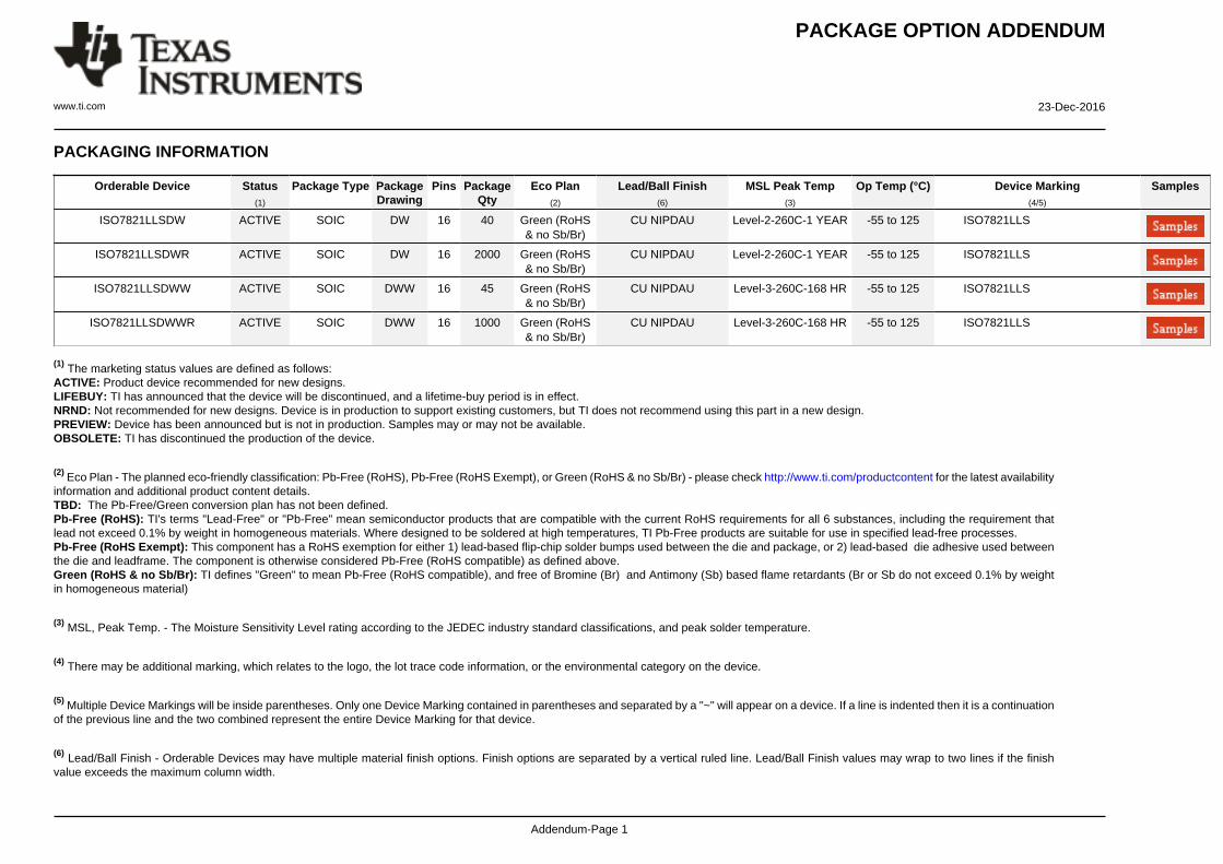
13 Mechanical, Packaging, and Orderable InformationThe following pages include mechanical, packaging, and orderable information. This information is the mostcurrent data available for the designated devices. This data is subject to change without notice and revision ofthis document. For browser-based versions of this data sheet, refer to the left-hand navigation.
ISO7821LLSDW ACTIVE SOIC DW 16 40 Green (RoHS& no Sb/Br)
CU NIPDAU Level-2-260C-1 YEAR -55 to 125 ISO7821LLS
ISO7821LLSDWR ACTIVE SOIC DW 16 2000 Green (RoHS& no Sb/Br)
CU NIPDAU Level-2-260C-1 YEAR -55 to 125 ISO7821LLS
ISO7821LLSDWW ACTIVE SOIC DWW 16 45 Green (RoHS& no Sb/Br)
CU NIPDAU Level-3-260C-168 HR -55 to 125 ISO7821LLS
ISO7821LLSDWWR ACTIVE SOIC DWW 16 1000 Green (RoHS& no Sb/Br)
CU NIPDAU Level-3-260C-168 HR -55 to 125 ISO7821LLS
(1) The marketing status values are defined as follows:ACTIVE: Product device recommended for new designs.LIFEBUY: TI has announced that the device will be discontinued, and a lifetime-buy period is in effect.NRND: Not recommended for new designs. Device is in production to support existing customers, but TI does not recommend using this part in a new design.PREVIEW: Device has been announced but is not in production. Samples may or may not be available.OBSOLETE: TI has discontinued the production of the device.
(2) Eco Plan - The planned eco-friendly classification: Pb-Free (RoHS), Pb-Free (RoHS Exempt), or Green (RoHS & no Sb/Br) - please check http://www.ti.com/productcontent for the latest availabilityinformation and additional product content details.TBD: The Pb-Free/Green conversion plan has not been defined.Pb-Free (RoHS): TI's terms "Lead-Free" or "Pb-Free" mean semiconductor products that are compatible with the current RoHS requirements for all 6 substances, including the requirement thatlead not exceed 0.1% by weight in homogeneous materials. Where designed to be soldered at high temperatures, TI Pb-Free products are suitable for use in specified lead-free processes.Pb-Free (RoHS Exempt): This component has a RoHS exemption for either 1) lead-based flip-chip solder bumps used between the die and package, or 2) lead-based die adhesive used betweenthe die and leadframe. The component is otherwise considered Pb-Free (RoHS compatible) as defined above.Green (RoHS & no Sb/Br): TI defines "Green" to mean Pb-Free (RoHS compatible), and free of Bromine (Br) and Antimony (Sb) based flame retardants (Br or Sb do not exceed 0.1% by weightin homogeneous material)
(3) MSL, Peak Temp. - The Moisture Sensitivity Level rating according to the JEDEC industry standard classifications, and peak solder temperature.
(4) There may be additional marking, which relates to the logo, the lot trace code information, or the environmental category on the device.
(5) Multiple Device Markings will be inside parentheses. Only one Device Marking contained in parentheses and separated by a "~" will appear on a device. If a line is indented then it is a continuationof the previous line and the two combined represent the entire Device Marking for that device.
(6) Lead/Ball Finish - Orderable Devices may have multiple material finish options. Finish options are separated by a vertical ruled line. Lead/Ball Finish values may wrap to two lines if the finishvalue exceeds the maximum column width.
Important Information and Disclaimer:The information provided on this page represents TI's knowledge and belief as of the date that it is provided. TI bases its knowledge and belief on informationprovided by third parties, and makes no representation or warranty as to the accuracy of such information. Efforts are underway to better integrate information from third parties. TI has taken andcontinues to take reasonable steps to provide representative and accurate information but may not have conducted destructive testing or chemical analysis on incoming materials and chemicals.TI and TI suppliers consider certain information to be proprietary, and thus CAS numbers and other limited information may not be available for release.
In no event shall TI's liability arising out of such information exceed the total purchase price of the TI part(s) at issue in this document sold by TI to Customer on an annual basis.
Images above are just a representation of the package family, actual package may vary.Refer to the product data sheet for package details.
DW 16 SOIC - 2.65 mm max heightSMALL OUTLINE INTEGRATED CIRCUIT
4040000-2/H
www.ti.com
PACKAGE OUTLINE
C
TYP10.639.97
2.65 MAX
14X 1.27
16X 0.510.31
2X8.89
TYP0.330.10
0 - 80.30.1
(1.4)
0.25GAGE PLANE
1.270.40
A
NOTE 3
10.510.1
BNOTE 4
7.67.4
4221009/B 07/2016
SOIC - 2.65 mm max heightDW0016BSOIC
NOTES: 1. All linear dimensions are in millimeters. Dimensions in parenthesis are for reference only. Dimensioning and tolerancing per ASME Y14.5M. 2. This drawing is subject to change without notice. 3. This dimension does not include mold flash, protrusions, or gate burrs. Mold flash, protrusions, or gate burrs shall not exceed 0.15 mm, per side. 4. This dimension does not include interlead flash. Interlead flash shall not exceed 0.25 mm, per side.5. Reference JEDEC registration MS-013.
1 16
0.25 C A B
98
PIN 1 IDAREA
SEATING PLANE
0.1 C
SEE DETAIL A
DETAIL ATYPICAL
SCALE 1.500
www.ti.com
EXAMPLE BOARD LAYOUT
(9.75)R0.05 TYP
0.07 MAXALL AROUND
0.07 MINALL AROUND
(9.3)
14X (1.27)
R0.05 TYP
16X (1.65)
16X (0.6)
14X (1.27)
16X (2)
16X (0.6)
4221009/B 07/2016
SOIC - 2.65 mm max heightDW0016BSOIC
SYMM
SYMM
SEEDETAILS
1
8 9
16
SYMM
HV / ISOLATION OPTION8.1 mm CLEARANCE/CREEPAGE
NOTES: (continued) 6. Publication IPC-7351 may have alternate designs. 7. Solder mask tolerances between and around signal pads can vary based on board fabrication site.
METAL SOLDER MASKOPENING
NON SOLDER MASKDEFINED
SOLDER MASK DETAILS
OPENINGSOLDER MASK METAL
SOLDER MASKDEFINED
LAND PATTERN EXAMPLESCALE:4X
SYMM
1
8 9
16
IPC-7351 NOMINAL7.3 mm CLEARANCE/CREEPAGE
SEEDETAILS
www.ti.com
EXAMPLE STENCIL DESIGN
R0.05 TYPR0.05 TYP
16X (1.65)
16X (0.6)
14X (1.27)
(9.75)
16X (2)
16X (0.6)
14X (1.27)
(9.3)
4221009/B 07/2016
SOIC - 2.65 mm max heightDW0016BSOIC
NOTES: (continued) 8. Laser cutting apertures with trapezoidal walls and rounded corners may offer better paste release. IPC-7525 may have alternate design recommendations. 9. Board assembly site may have different recommendations for stencil design.
SYMM
SYMM
1
8 9
16
HV / ISOLATION OPTION8.1 mm CLEARANCE/CREEPAGE
SOLDER PASTE EXAMPLEBASED ON 0.125 mm THICK STENCIL
SCALE:4X
SYMM
SYMM
1
8 9
16
IPC-7351 NOMINAL7.3 mm CLEARANCE/CREEPAGE
IMPORTANT NOTICE
Texas Instruments Incorporated (TI) reserves the right to make corrections, enhancements, improvements and other changes to itssemiconductor products and services per JESD46, latest issue, and to discontinue any product or service per JESD48, latest issue. Buyersshould obtain the latest relevant information before placing orders and should verify that such information is current and complete.TI’s published terms of sale for semiconductor products (http://www.ti.com/sc/docs/stdterms.htm) apply to the sale of packaged integratedcircuit products that TI has qualified and released to market. Additional terms may apply to the use or sale of other types of TI products andservices.Reproduction of significant portions of TI information in TI data sheets is permissible only if reproduction is without alteration and isaccompanied by all associated warranties, conditions, limitations, and notices. TI is not responsible or liable for such reproduceddocumentation. Information of third parties may be subject to additional restrictions. Resale of TI products or services with statementsdifferent from or beyond the parameters stated by TI for that product or service voids all express and any implied warranties for theassociated TI product or service and is an unfair and deceptive business practice. TI is not responsible or liable for any such statements.Buyers and others who are developing systems that incorporate TI products (collectively, “Designers”) understand and agree that Designersremain responsible for using their independent analysis, evaluation and judgment in designing their applications and that Designers havefull and exclusive responsibility to assure the safety of Designers' applications and compliance of their applications (and of all TI productsused in or for Designers’ applications) with all applicable regulations, laws and other applicable requirements. Designer represents that, withrespect to their applications, Designer has all the necessary expertise to create and implement safeguards that (1) anticipate dangerousconsequences of failures, (2) monitor failures and their consequences, and (3) lessen the likelihood of failures that might cause harm andtake appropriate actions. Designer agrees that prior to using or distributing any applications that include TI products, Designer willthoroughly test such applications and the functionality of such TI products as used in such applications.TI’s provision of technical, application or other design advice, quality characterization, reliability data or other services or information,including, but not limited to, reference designs and materials relating to evaluation modules, (collectively, “TI Resources”) are intended toassist designers who are developing applications that incorporate TI products; by downloading, accessing or using TI Resources in anyway, Designer (individually or, if Designer is acting on behalf of a company, Designer’s company) agrees to use any particular TI Resourcesolely for this purpose and subject to the terms of this Notice.TI’s provision of TI Resources does not expand or otherwise alter TI’s applicable published warranties or warranty disclaimers for TIproducts, and no additional obligations or liabilities arise from TI providing such TI Resources. TI reserves the right to make corrections,enhancements, improvements and other changes to its TI Resources. TI has not conducted any testing other than that specificallydescribed in the published documentation for a particular TI Resource.Designer is authorized to use, copy and modify any individual TI Resource only in connection with the development of applications thatinclude the TI product(s) identified in such TI Resource. NO OTHER LICENSE, EXPRESS OR IMPLIED, BY ESTOPPEL OR OTHERWISETO ANY OTHER TI INTELLECTUAL PROPERTY RIGHT, AND NO LICENSE TO ANY TECHNOLOGY OR INTELLECTUAL PROPERTYRIGHT OF TI OR ANY THIRD PARTY IS GRANTED HEREIN, including but not limited to any patent right, copyright, mask work right, orother intellectual property right relating to any combination, machine, or process in which TI products or services are used. Informationregarding or referencing third-party products or services does not constitute a license to use such products or services, or a warranty orendorsement thereof. Use of TI Resources may require a license from a third party under the patents or other intellectual property of thethird party, or a license from TI under the patents or other intellectual property of TI.TI RESOURCES ARE PROVIDED “AS IS” AND WITH ALL FAULTS. TI DISCLAIMS ALL OTHER WARRANTIES ORREPRESENTATIONS, EXPRESS OR IMPLIED, REGARDING RESOURCES OR USE THEREOF, INCLUDING BUT NOT LIMITED TOACCURACY OR COMPLETENESS, TITLE, ANY EPIDEMIC FAILURE WARRANTY AND ANY IMPLIED WARRANTIES OFMERCHANTABILITY, FITNESS FOR A PARTICULAR PURPOSE, AND NON-INFRINGEMENT OF ANY THIRD PARTY INTELLECTUALPROPERTY RIGHTS. TI SHALL NOT BE LIABLE FOR AND SHALL NOT DEFEND OR INDEMNIFY DESIGNER AGAINST ANY CLAIM,INCLUDING BUT NOT LIMITED TO ANY INFRINGEMENT CLAIM THAT RELATES TO OR IS BASED ON ANY COMBINATION OFPRODUCTS EVEN IF DESCRIBED IN TI RESOURCES OR OTHERWISE. IN NO EVENT SHALL TI BE LIABLE FOR ANY ACTUAL,DIRECT, SPECIAL, COLLATERAL, INDIRECT, PUNITIVE, INCIDENTAL, CONSEQUENTIAL OR EXEMPLARY DAMAGES INCONNECTION WITH OR ARISING OUT OF TI RESOURCES OR USE THEREOF, AND REGARDLESS OF WHETHER TI HAS BEENADVISED OF THE POSSIBILITY OF SUCH DAMAGES.Unless TI has explicitly designated an individual product as meeting the requirements of a particular industry standard (e.g., ISO/TS 16949and ISO 26262), TI is not responsible for any failure to meet such industry standard requirements.Where TI specifically promotes products as facilitating functional safety or as compliant with industry functional safety standards, suchproducts are intended to help enable customers to design and create their own applications that meet applicable functional safety standardsand requirements. Using products in an application does not by itself establish any safety features in the application. Designers mustensure compliance with safety-related requirements and standards applicable to their applications. Designer may not use any TI products inlife-critical medical equipment unless authorized officers of the parties have executed a special contract specifically governing such use.Life-critical medical equipment is medical equipment where failure of such equipment would cause serious bodily injury or death (e.g., lifesupport, pacemakers, defibrillators, heart pumps, neurostimulators, and implantables). Such equipment includes, without limitation, allmedical devices identified by the U.S. Food and Drug Administration as Class III devices and equivalent classifications outside the U.S.TI may expressly designate certain products as completing a particular qualification (e.g., Q100, Military Grade, or Enhanced Product).Designers agree that it has the necessary expertise to select the product with the appropriate qualification designation for their applicationsand that proper product selection is at Designers’ own risk. Designers are solely responsible for compliance with all legal and regulatoryrequirements in connection with such selection.Designer will fully indemnify TI and its representatives against any damages, costs, losses, and/or liabilities arising out of Designer’s non-compliance with the terms and provisions of this Notice.