Page 1
High‐Voltage DC and RF Power Reliability of GaN HEMTs
J. A. del Alamo and J. Joh*Microsystems Technology Laboratories, MIT, Cambridge, MA (USA)
*presently with Texas Instruments, Dallas, TX (USA)
ICNS 2011Glasgow, July 10-15, 2011
Acknowledgements: ARL (DARPA-WBGS program), ONR (DRIFT-MURI program)Accel-RF Corporation
Page 2
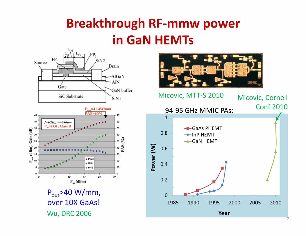
Micovic, Cornell Conf 201094‐95 GHz MMIC PAs:
Micovic, MTT‐S 2010
Pout>40 W/mm, over 10X GaAs! Wu, DRC 2006
Breakthrough RF‐mmw power in GaN HEMTs
2
Page 3
3
GaN HEMTs in the field
Counter‐IED Systems (CREW) 200 W GaN HEMT for
cellular base station Kawano, APMC 2005
100 mm GaN‐on‐SiCvolume manufacturingPalmour, MTT‐S 2010
Page 4
Recent great strides in RF power reliability
4
28 V RF oper. life > 2 years (X‐band, 3 dB comp., ~150oC)Kolias, MTT‐S 2010
MTTF=1x10⁷ h at 47 V (C‐band, 5 dB comp., ~150oC)Yamasaki, MTT‐S 2010
MTTF=7x10⁷ h at 28 V (40 GHz, 1.5 dB comp., ~150oC)Heying, MTT‐S 2010
Page 5
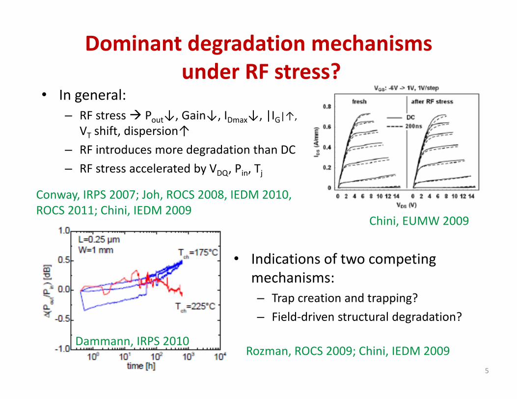
• In general: – RF stress Pout↓, Gain↓, IDmax↓, |IG|↑,
VT shift, dispersion↑– RF introduces more degradation than DC– RF stress accelerated by VDQ, Pin, Tj
Dominant degradation mechanismsunder RF stress?
5
Conway, IRPS 2007; Joh, ROCS 2008, IEDM 2010, ROCS 2011; Chini, IEDM 2009
• Indications of two competing mechanisms: – Trap creation and trapping?– Field‐driven structural degradation?
Chini, EUMW 2009
Rozman, ROCS 2009; Chini, IEDM 2009Dammann, IRPS 2010
Page 6
Outline
1. RF power reliability concerns2. Methodology for RF reliability experiments3. Electrical and structural results4. Discussion: the role of gate placement5. Conclusions
6
Page 7
RF power reliability concerns
7
OFF and semi‐ON high‐voltage DC stress :– Degradation of IDmax, RD, IGoff– VT shift– Electron trapping– Trap creation– Formation of grooves and pits under drain‐end of gate
High‐power DC stress:– Not accessible to DC stress experiments– Device blows up instantly
ON DC stress:– Mostly benign
Page 8
RF experiment flowchart:conventional approach
8
Limitations:• Bias point shifts during stress• Limited RF characterization• No DC characterization• No trap characterization• If examining different RF
conditions, RF characterization confusing
START
RF StressPout, PAE, Gain, IDQ, IGQ
END
Tstress
Page 9
RF experiment flowchart: improved approach (I)
New features:• RF and DC characterization under
standardized conditions • At beginning, end and periodically
through experiment
Limitations:• Limited characterization• Characterization temperature
cannot be too different from stress temperature
• Cannot separate trapping from “permanent” degradation
9
START
RF Stress
Short Characterization (DC, RF)
End?
YES
NO
Tstress
Tbase
END
Short Characterization (DC, RF)
Page 10
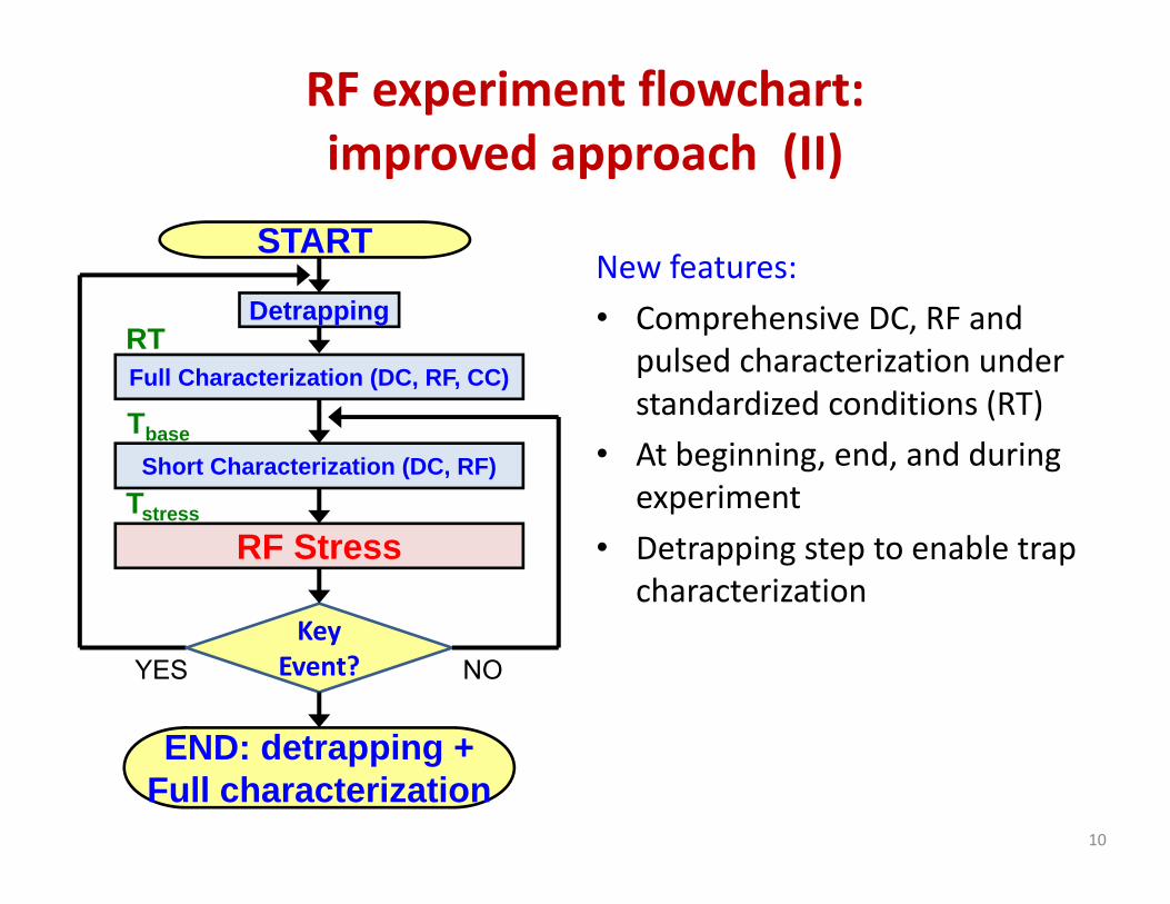
RF experiment flowchart: improved approach (II)
New features:• Comprehensive DC, RF and
pulsed characterization under standardized conditions (RT)
• At beginning, end, and during experiment
• Detrapping step to enable trap characterization
10
Full Characterization (DC, RF, CC)
START
RF Stress
Short Characterization (DC, RF)
Key Event?
END: detrapping +Full characterization
YES
Detrapping
NO
Tstress
RT
Tbase
Page 11
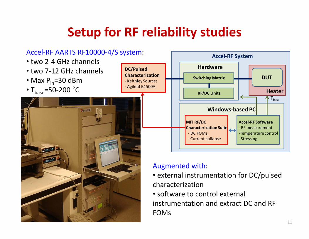
Setup for RF reliability studies
11
DC/Pulsed Characterization‐ KeithleySources‐ Agilent B1500A
Windows‐based PC
Accel‐RF System
Hardware
MIT RF/DC Characterization Suite‐ DC FOMs‐ Current collapse
DUTSwitching Matrix
RF/DC Units
Accel‐RF Software‐ RF measurement‐Temperature control‐ Stressing
TbaseHeater
Augmented with:• external instrumentation for DC/pulsed characterization• software to control external instrumentation and extract DC and RF FOMs
Accel‐RF AARTS RF10000‐4/S system:• two 2‐4 GHz channels• two 7‐12 GHz channels • Max Pin=30 dBm• Tbase=50‐200 °C
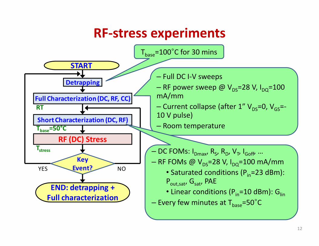
Page 12
RF‐stress experiments
12
Full Characterization (DC, RF, CC)
START
RF (DC) Stress
Short Characterization (DC, RF)
Key Event?
END: detrapping +Full characterization
YES
Detrapping
NO
Tstress
RT
Tbase=50°C
Tbase=100°C for 30 mins
– Full DC I‐V sweeps– RF power sweep @ VDS=28 V, IDQ=100 mA/mm– Current collapse (after 1” VDS=0, VGS=‐10 V pulse)– Room temperature
– DC FOMs: IDmax, RS, RD, VT, IGoff, …– RF FOMs @ VDS=28 V, IDQ=100 mA/mm
• Saturated conditions (Pin=23 dBm): Pout,sat, Gsat, PAE• Linear conditions (Pin=10 dBm): Glin
– Every few minutes at Tbase=50°C
Page 13
0
5
10
15
20
25
0
2
4
6
8
10
12
14
10 15 20 25 30
PAE (%
)
Gain (d
B)
Pin (dBm)
PAE
Gain
RF stress experiments: Pin step‐stress
13
• Motivation: – higher Pin larger V waveform at output
• MMIC: – single‐stage internally‐matched– 4x100 μm GaN HEMT (OFF-state Vcrit >60 V at RT)– Gate centered in S‐D gap
• Step Pin stress:– VDS = 40 V, IDQ = 100 mA/mm– Pin = 0 (DC), 1, 20‐27 dBm– 300 min stress at each step– Tstress=50 °C (Tj=110‐230°C) VDS=40 V, IDQ=100 mA/mm
Joh, ROCS 2011
Page 14
0 10 20 30 40 50 6029
30
31
32
33
Time (hr)P
out (d
Bm
)0 10 20 30 40 50 60
0
5
10
15
20
25
30
Time (hr)
Pin (d
Bm
)
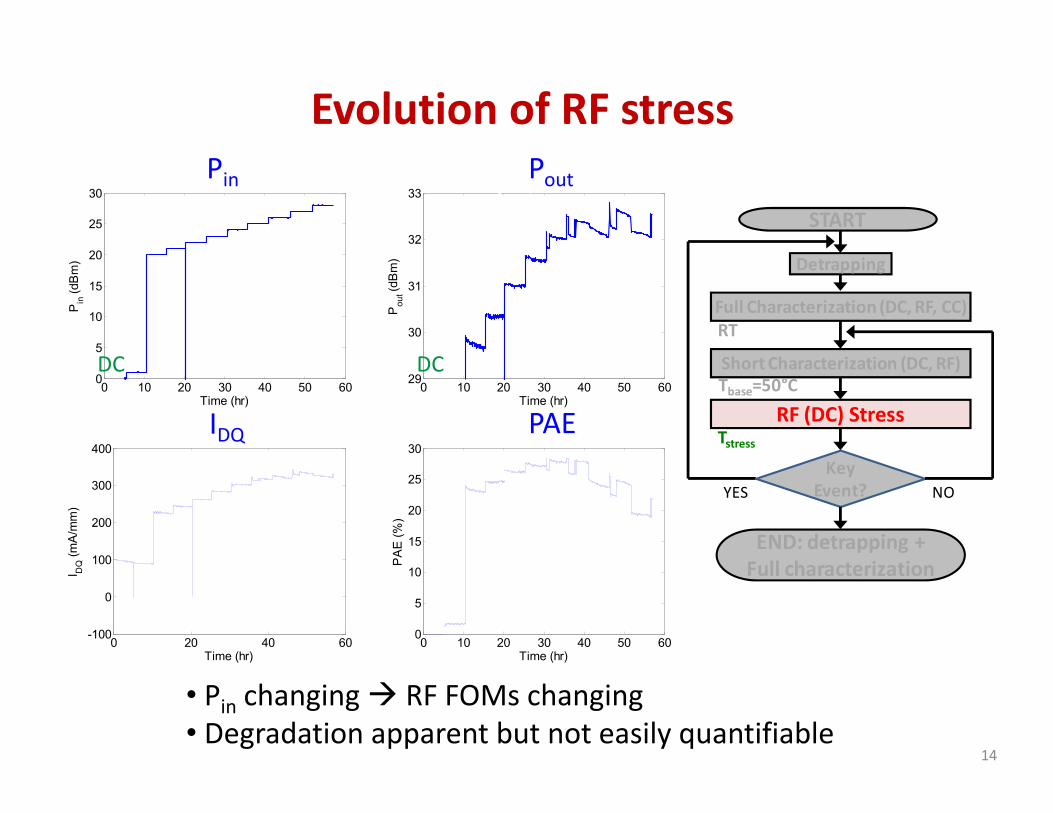
Evolution of RF stress
14
• Pin changing RF FOMs changing• Degradation apparent but not easily quantifiable
Pout
Gain
Pin Pout
IDQ PAE
Full Characterization (DC, RF, CC)
START
RF (DC) Stress
Short Characterization (DC, RF)
Key Event?
END: detrapping +Full characterization
YES
Detrapping
NO
Tstress
RT
Tbase=50°CDC DC
0 20 40 60-100
0
100
200
300
400
Time (hr)
I DQ (m
A/m
m)
0 10 20 30 40 50 600
5
10
15
20
25
30
Time (hr)
PA
E (%
)
Page 15
RF FOM during short characterization
15
• Mild degradation under DC and low Pin• Adding RF increases degradation: Pin ↑ Pout ↓
Full Characterization (DC, RF, CC)
START
RF (DC) Stress
Short Characterization (DC, RF)
Key Event?
END: detrapping +Full characterization
YES
Detrapping
NO
Tstress
RT
Tbase=50°C
Pout at Pin=23 dBm, Glin at Pin=10 dBmVDS=28 V, IDQ=100 mA/mm, Tbase=50°C
Page 16
1.E-06
1.E-05
1.E-04
1.E-03
1.E-02
1.E-01
1.E+00
1.E+01
0.8
0.9
1
1.1
1.2
0 1000 2000 3000
|I Gof
f| (m
A/m
m)
I Dm
ax/I D
max
(0),
R/R
(0)
Time (min)
IDmax
RS
RD
IGoff
DC|Pin=1 20 21 22 23 24 25 26 27 dBm
DC FOM during short characterization
16
• Mild degradation under DC and low Pin• At Pin=20 dBm, step degradation in IGoff• Beyond Pin=20 dBm, increasing degradation of IDmax and RD
Tbase=50°C
Full Characterization (DC, RF, CC)
START
RF (DC) Stress
Short Characterization (DC, RF)
Key Event?
END: detrapping +Full characterization
YES
Detrapping
NO
Tstress
RT
Tbase=50°C
Page 17
29
30
31
32
33
0123456789
‐10 0 10 20 30
Saturated P o
ut(dBm
)
Perm
anen
t IDmaxDegrada
tion (%
)Cu
rren
t Collapse (%
)
Stress Input Power Pin (dBm)
Initial
DC RF
Pout
CurrentCollapse
Δ|IDmax|
Tbase=RT
DC/RF/CC full characterization
17
• Beyond Pin=20 dBm:― Sharp Pout degradation― Permanent degradation of IDmax― Increased CC evidence of new trap creation
Full Characterization (DC, RF, CC)
START
RF (DC) Stress
Short Characterization (DC, RF)
Key Event?
END: detrapping +Full characterization
YES
Detrapping
NO
Tstress
RT
Tbase=50°C
100 °C
Page 18
Structural degradation (planar view)
• Pit formation along drain end of gate edge• Similar to DC high voltage OFF‐state stress
18
SEM AFM
DC OFF‐state stress, VDG=50 V, 1000 min, ~150oCMakaram, APL 2010
Page 19
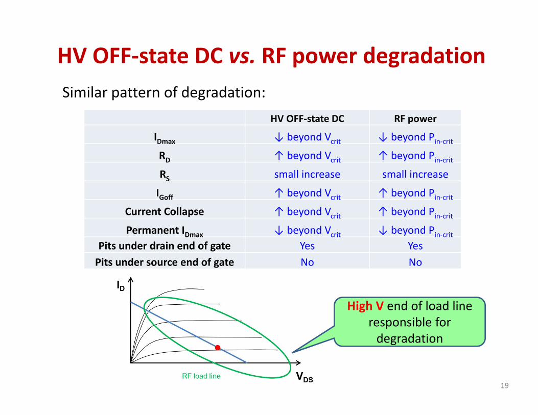
HV OFF‐state DC vs. RF power degradation
19
Similar pattern of degradation:
High V end of load line responsible for degradation
HV OFF‐state DC RF power
IDmax ↓ beyond Vcrit ↓ beyond Pin‐critRD ↑ beyond Vcrit ↑ beyond Pin‐critRS small increase small increase
IGoff ↑ beyond Vcrit ↑ beyond Pin‐critCurrent Collapse ↑ beyond Vcrit ↑ beyond Pin‐critPermanent IDmax ↓ beyond Vcrit ↓ beyond Pin‐crit
Pits under drain end of gate Yes YesPits under source end of gate No No
Page 20
Step Pin stress: Offset Gate
1.E-03
1.E-02
1.E-01
1.E+00
1.E+01
0
0.5
1
1.5
2
2.5
3
0 300 600 900 1200
|I Gof
f| (m
A/m
m)
I Dm
ax/I D
max
(0),
R/R
(0)
Time (min)
IDmax
RS
RD
IGoff
Inner loop (50°C)
DC RF Pin=20 23 26 dBm
13
13.5
14
14.5
15
30
30.5
31
31.5
32
32.5
0 300 600 900 1200
Small Signa
l Gain Glin(dB)
Saturated P o
ut(dBm
)
Time (min)
Gain
Pout
DC RF Pin=20 23 26 dBm
Inner loop (50°C)
RF FOMs DC FOMs
Joh, IEDM 2010
• Increased degradation under high Pin• No IGoff degradation• Degradation of IDmax and RS, not RD
20
Offset gate devices (LGS<LGD): OFF-state Vcrit > 80 V at T=150°C
Tj~170°C by adjusting Tbase
Page 21
HV OFF‐state DC vs. RF power degradation
21
Different pattern of degradation:
High V end of load line NOT responsible for
degradation
HV OFF‐state DC RF power
IDmax ↓ beyond Vcrit ↓ beyond Pin‐critRD ↑ beyond Vcrit ↑ beyond Pin‐critRS small increase ↑↑ beyond Pin‐critIGoff ↑ beyond Vcrit No
Current Collapse ↑ beyond Vcrit ↑ beyond Pin‐critPermanent IDmax ↓ beyond Vcrit ↓ beyond Pin‐crit
Pits under drain end of gate Yes NoPits under source end of gate No No
Page 22
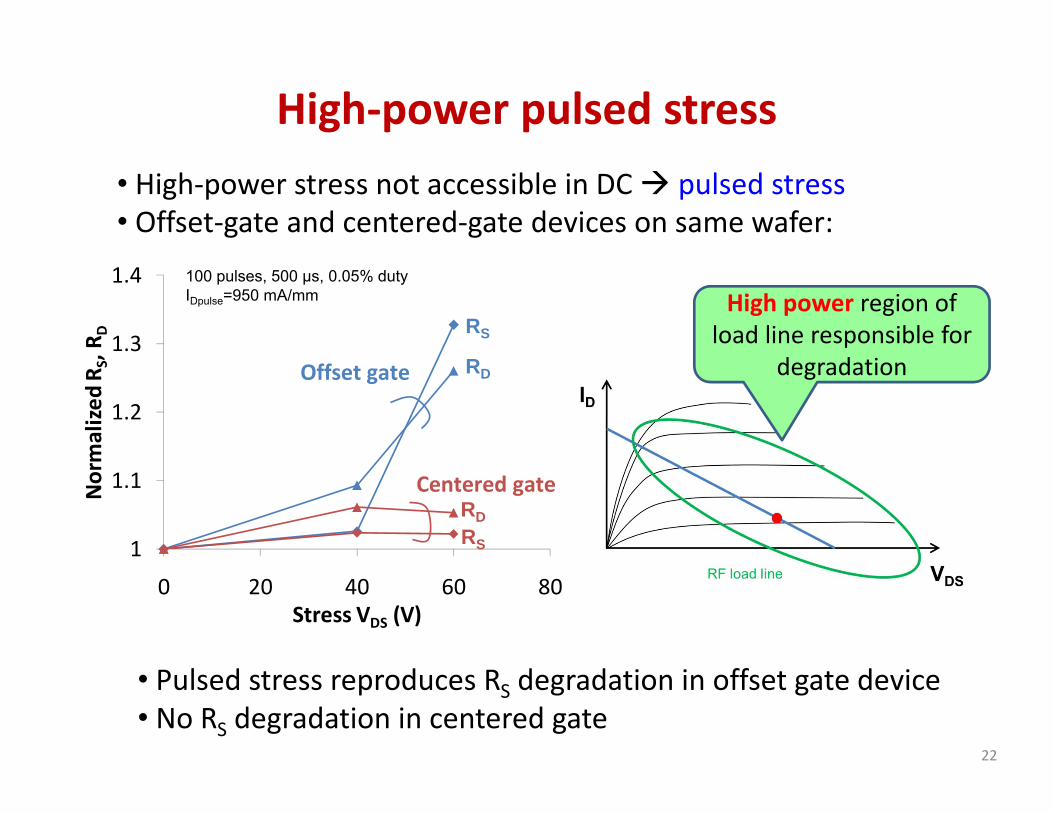
High‐power pulsed stress
22
• Pulsed stress reproduces RS degradation in offset gate device• No RS degradation in centered gate
1
1.1
1.2
1.3
1.4
0 20 40 60 80
Normalized
RS, R D
Stress VDS (V)
Offset gate
Centered gate
RS
RD
RDRS1
1.1
1.2
1.3
1.4
0 20 40 60 80
Normalized
RS, R D
Stress VDS (V)
Offset gate
Centered gate
RS
RD
RDRS
100 pulses, 500 μs, 0.05% dutyIDpulse=950 mA/mm
• High‐power stress not accessible in DC pulsed stress• Offset‐gate and centered‐gate devices on same wafer:
High power region of load line responsible for
degradation
Page 23
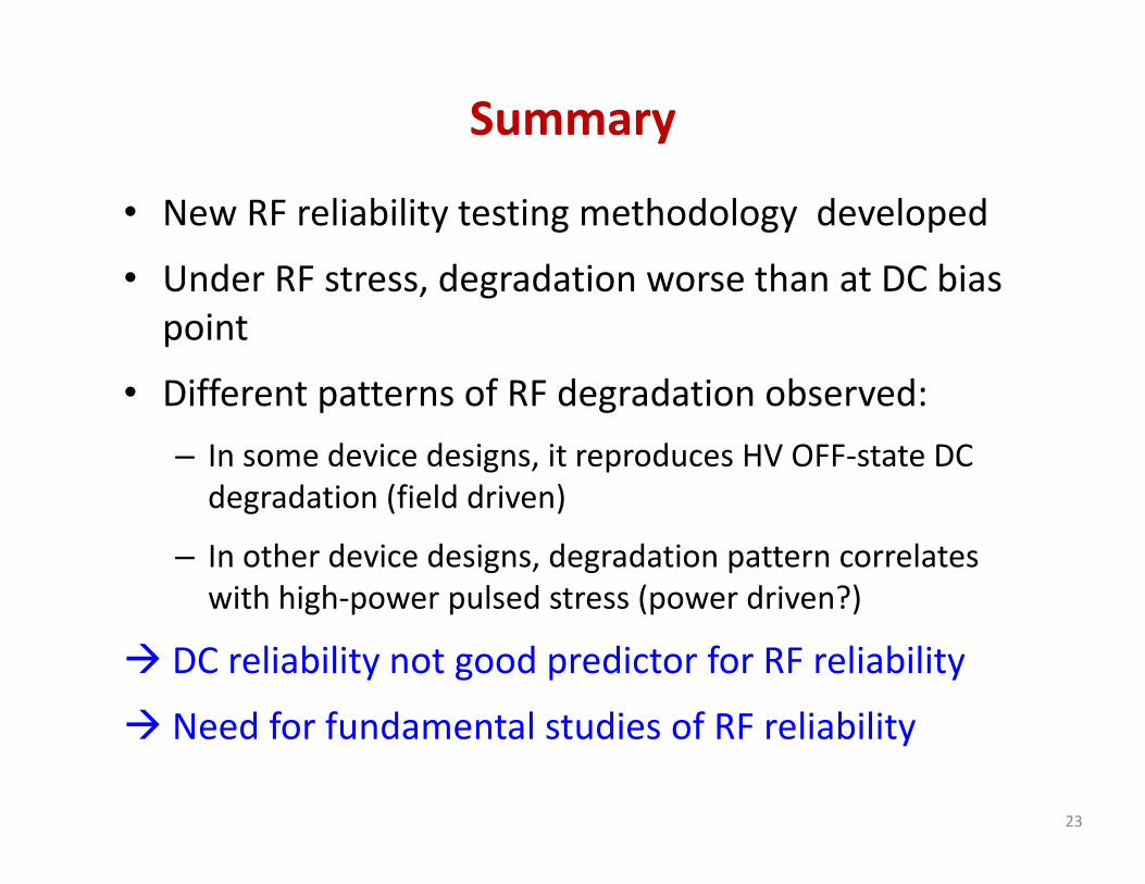
Summary
• New RF reliability testing methodology developed
• Under RF stress, degradation worse than at DC bias point
• Different patterns of RF degradation observed:– In some device designs, it reproduces HV OFF‐state DC degradation (field driven)
– In other device designs, degradation pattern correlates with high‐power pulsed stress (power driven?)
DC reliability not good predictor for RF reliability
Need for fundamental studies of RF reliability
23