Quantification of carbon contamination under electron beam irradiation in a scanning transmission electron microscope and its suppression by plasma cleaning AJV Griffiths and T Walther Department of Electronic & Electrical Engineering, University of Sheffield, Sir Frederick Mappin Building, Mappin Street, Sheffield S1 3JD, UK [email protected]Abstract. We have measured the build-up of carbon surface contamination as a function of time and irradiated area size for various specimens in a JEOL 2010F (scanning) transmission electron microscope, employing both t/λ mapping with our Gatan imaging filter and recording changes in annular dark-field image intensity. It is shown that the total number of carbon atoms deposited per time for a given beam intensity is roughly constant at room temperature for as- received specimens while it is significantly lower for plasma cleaned specimens. This explains why contamination is generally only an issue at the highest magnifications where the contamination regions become smaller and the carbon layers correspondingly thicker. A Fischione plasma cleaner was then used to remove these carbon layers, and the rate of carbon removal has been determined for contamination spots produced in stationary spot mode as well as for extended regions scanned for a minute so that optimal cleaning times can be chosen. 1. Introduction The quantitative analysis of scanning transmission electron microscopy data, images as well as spectra, is often hampered by surface contamination during electron irradiation. The gradual build-up of carbon layers on the specimen will reduce the image contrast and increase the signal from C K-edge energy losses and corresponding X-rays, thereby causing artefacts in spectroscopy. Contamination is caused by the cracking of hydrocarbons present both in the vacuum chamber and on the specimen and their subsequent surface diffusion to the site being irradiated [1,2]. Although our JEOL2010F field-emission gun (scanning) transmission electron microscope (FEG-(S)TEM) is equipped with a completely dry vacuum pumping system that involves only scroll, turbo molecular drag and ion getter pumps but no rotary or oil diffusion pumps, carbon contamination is still an issue when imaging or scanning small regions at high magnifications. For this study, the microscope has been tested just before a bake-out of its column was due to improve vacuum levels. We have calculated quantitatively the build-up of carbon surface contamination as a function of time and irradiated area size for different specimens and holders. A Fischione Model 1020 high-frequency argon/oxygen plasma cleaner was then used to remove these carbon layers, and the rate of carbon removal has been determined so that optimal cleaning times can be determined. 2. Experimental Samples of C, InAs and InGaAs were investigated in the JEOL 2010F FEG-(S)TEM in scan or spot mode at nominal magnifications between 60kX and 4000kX (4MX), using an electron beam ~0.5nm in diameter and with ~0.1nA current (nominal spot size M, 100-130μA emission, 197kV). The Electron Microscopy and Analysis Group Conference 2009 (EMAG 2009) IOP Publishing Journal of Physics: Conference Series 241 (2010) 012017 doi:10.1088/1742-6596/241/1/012017 c 2010 Published under licence by IOP Publishing Ltd 1
Transcript
Quantification of carbon contamination under electron beam
irradiation in a scanning transmission electron microscope
and its suppression by plasma cleaning
AJV Griffiths and T Walther
Department of Electronic & Electrical Engineering, University of Sheffield, Sir
Frederick Mappin Building, Mappin Street, Sheffield S1 3JD, UK
Abstract. We have measured the build-up of carbon surface contamination as a function of
time and irradiated area size for various specimens in a JEOL 2010F (scanning) transmission
electron microscope, employing both t/λ mapping with our Gatan imaging filter and recording
changes in annular dark-field image intensity. It is shown that the total number of carbon atoms
deposited per time for a given beam intensity is roughly constant at room temperature for as-
received specimens while it is significantly lower for plasma cleaned specimens. This explains
why contamination is generally only an issue at the highest magnifications where the
contamination regions become smaller and the carbon layers correspondingly thicker. A
Fischione plasma cleaner was then used to remove these carbon layers, and the rate of carbon
removal has been determined for contamination spots produced in stationary spot mode as well
as for extended regions scanned for a minute so that optimal cleaning times can be chosen.
1. Introduction
The quantitative analysis of scanning transmission electron microscopy data, images as well as
spectra, is often hampered by surface contamination during electron irradiation. The gradual build-up
of carbon layers on the specimen will reduce the image contrast and increase the signal from C K-edge
energy losses and corresponding X-rays, thereby causing artefacts in spectroscopy.
Contamination is caused by the cracking of hydrocarbons present both in the vacuum chamber and
on the specimen and their subsequent surface diffusion to the site being irradiated [1,2]. Although our
JEOL2010F field-emission gun (scanning) transmission electron microscope (FEG-(S)TEM) is
equipped with a completely dry vacuum pumping system that involves only scroll, turbo molecular
drag and ion getter pumps but no rotary or oil diffusion pumps, carbon contamination is still an issue
when imaging or scanning small regions at high magnifications. For this study, the microscope has
been tested just before a bake-out of its column was due to improve vacuum levels. We have
calculated quantitatively the build-up of carbon surface contamination as a function of time and
irradiated area size for different specimens and holders. A Fischione Model 1020 high-frequency
argon/oxygen plasma cleaner was then used to remove these carbon layers, and the rate of carbon
removal has been determined so that optimal cleaning times can be determined.
2. Experimental Samples of C, InAs and InGaAs were investigated in the JEOL 2010F FEG-(S)TEM in scan or spot mode at nominal magnifications between 60kX and 4000kX (4MX), using an electron beam ~0.5nm
in diameter and with ~0.1nA current (nominal spot size M, 100-130µA emission, 197kV). The
Electron Microscopy and Analysis Group Conference 2009 (EMAG 2009) IOP PublishingJournal of Physics: Conference Series 241 (2010) 012017 doi:10.1088/1742-6596/241/1/012017
electron beam was either held stationary (spot mode) or raster scanned over square regions (scan mode). In order to facilitate quantitative evaluation, usually several frames of 1min exposures were taken at successively smaller magnifications so that the regions scanned at e.g. 4MX times were then imaged at 1MX times, 250kX and 60kX, revealing a superposition of the corresponding carbon contamination layers, almost square in size if drift was small, in the final image.
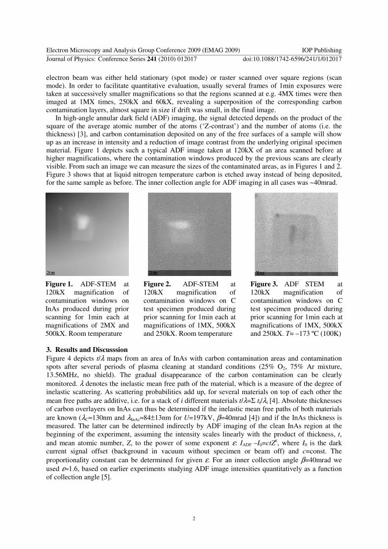
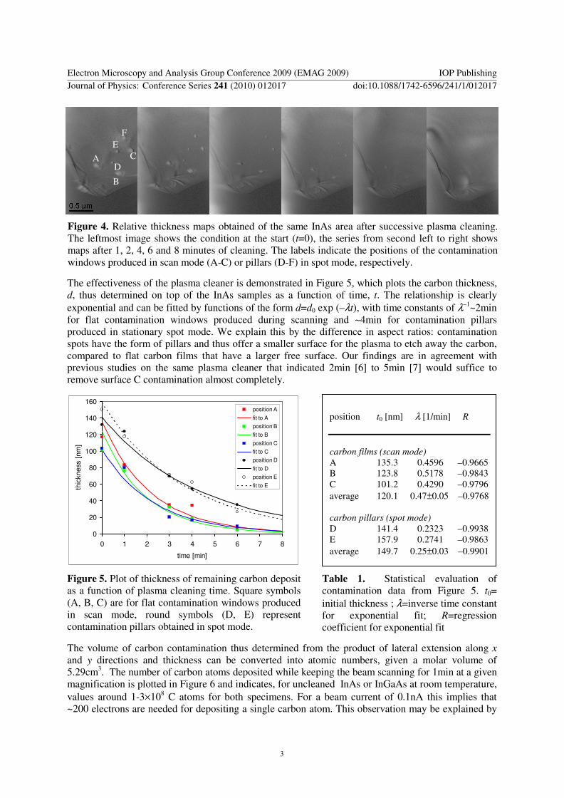
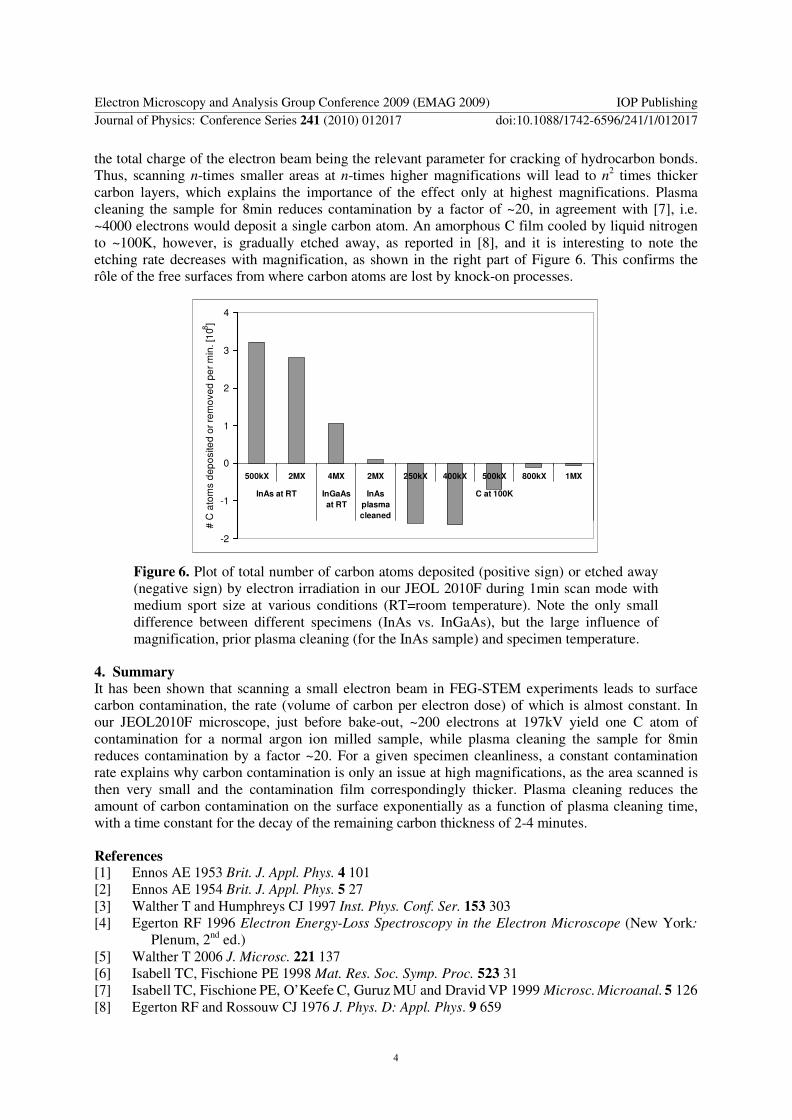
In high-angle annular dark field (ADF) imaging, the signal detected depends on the product of the square of the average atomic number of the atoms (‘Z-contrast’) and the number of atoms (i.e. the thickness) [3], and carbon contamination deposited on any of the free surfaces of a sample will show up as an increase in intensity and a reduction of image contrast from the underlying original specimen material. Figure 1 depicts such a typical ADF image taken at 120kX of an area scanned before at higher magnifications, where the contamination windows produced by the previous scans are clearly visible. From such an image we can measure the sizes of the contaminated areas, as in Figures 1 and 2. Figure 3 shows that at liquid nitrogen temperature carbon is etched away instead of being deposited, for the same sample as before. The inner collection angle for ADF imaging in all cases was ~40mrad.
Figure 1. ADF-STEM at
120kX magnification of
contamination windows on
InAs produced during prior
scanning for 1min each at
magnifications of 2MX and
500kX. Room temperature
Figure 2. ADF-STEM at
120kX magnification of
contamination windows on C
test specimen produced during
prior scanning for 1min each at
magnifications of 1MX, 500kX
and 250kX. Room temperature
Figure 3. ADF STEM at
120kX magnification of
contamination windows on C
test specimen produced during
prior scanning for 1min each at
magnifications of 1MX, 500kX
and 250kX. T= –173 ºC (100K)
3. Results and Discusssion
Figure 4 depicts t/λ maps from an area of InAs with carbon contamination areas and contamination
spots after several periods of plasma cleaning at standard conditions (25% O2, 75% Ar mixture,
13.56MHz, no shield). The gradual disappearance of the carbon contamination can be clearly
monitored. λ denotes the inelastic mean free path of the material, which is a measure of the degree of
inelastic scattering. As scattering probabilities add up, for several materials on top of each other the
mean free paths are additive, i.e. for a stack of i different materials t/λ=Σ ti/λi [4]. Absolute thicknesses
of carbon overlayers on InAs can thus be determined if the inelastic mean free paths of both materials
are known (λC≈130nm and λInAs≈84±13nm for U=197kV, β=40mrad [4]) and if the InAs thickness is
measured. The latter can be determined indirectly by ADF imaging of the clean InAs region at the
beginning of the experiment, assuming the intensity scales linearly with the product of thickness, t,
and mean atomic number, Z, to the power of some exponent ε: IADF –I0=ctZε, where I0 is the dark
current signal offset (background in vacuum without specimen or beam off) and c=const. The
proportionality constant can be determined for given ε. For an inner collection angle β=40mrad we
used ε≈1.6, based on earlier experiments studying ADF image intensities quantitatively as a function
of collection angle [5].
Electron Microscopy and Analysis Group Conference 2009 (EMAG 2009) IOP PublishingJournal of Physics: Conference Series 241 (2010) 012017 doi:10.1088/1742-6596/241/1/012017
2
Figure 4. Relative thickness maps obtained of the same InAs area after successive plasma cleaning.
The leftmost image shows the condition at the start (t=0), the series from second left to right shows
maps after 1, 2, 4, 6 and 8 minutes of cleaning. The labels indicate the positions of the contamination
windows produced in scan mode (A-C) or pillars (D-F) in spot mode, respectively.
The effectiveness of the plasma cleaner is demonstrated in Figure 5, which plots the carbon thickness,
d, thus determined on top of the InAs samples as a function of time, t. The relationship is clearly
exponential and can be fitted by functions of the form d=d0 exp (–λt), with time constants of λ–1~2min
for flat contamination windows produced during scanning and ~4min for contamination pillars
produced in stationary spot mode. We explain this by the difference in aspect ratios: contamination
spots have the form of pillars and thus offer a smaller surface for the plasma to etch away the carbon,
compared to flat carbon films that have a larger free surface. Our findings are in agreement with
previous studies on the same plasma cleaner that indicated 2min [6] to 5min [7] would suffice to
remove surface C contamination almost completely.
0
20
40
60
80
100
120
140
160
0 1 2 3 4 5 6 7 8
time [min]
thic
kne
ss [
nm
]
position A
fit to A
position B
fit to B
position C
fit to C
position D
fit to D
position E
fit to E
Figure 5. Plot of thickness of remaining carbon deposit
as a function of plasma cleaning time. Square symbols
(A, B, C) are for flat contamination windows produced
in scan mode, round symbols (D, E) represent
contamination pillars obtained in spot mode.
Table 1. Statistical evaluation of
contamination data from Figure 5. t0=
initial thickness ; λ=inverse time constant
for exponential fit; R=regression
coefficient for exponential fit
The volume of carbon contamination thus determined from the product of lateral extension along x
and y directions and thickness can be converted into atomic numbers, given a molar volume of
5.29cm3. The number of carbon atoms deposited while keeping the beam scanning for 1min at a given
magnification is plotted in Figure 6 and indicates, for uncleaned InAs or InGaAs at room temperature,
values around 1-3×10⁸ C atoms for both specimens. For a beam current of 0.1nA this implies that
~200 electrons are needed for depositing a single carbon atom. This observation may be explained by
position t0 [nm] λ [1/min] R
carbon films (scan mode)
A 135.3 0.4596 –0.9665
B 123.8 0.5178 –0.9843
C 101.2 0.4290 –0.9796
average 120.1 0.47±0.05 –0.9768
carbon pillars (spot mode)
D 141.4 0.2323 –0.9938
E 157.9 0.2741 –0.9863
average 149.7 0.25±0.03 –0.9901
A
B
C
D
E
F
Electron Microscopy and Analysis Group Conference 2009 (EMAG 2009) IOP PublishingJournal of Physics: Conference Series 241 (2010) 012017 doi:10.1088/1742-6596/241/1/012017
3
the total charge of the electron beam being the relevant parameter for cracking of hydrocarbon bonds.
Thus, scanning n-times smaller areas at n-times higher magnifications will lead to n2 times thicker
carbon layers, which explains the importance of the effect only at highest magnifications. Plasma
cleaning the sample for 8min reduces contamination by a factor of ~20, in agreement with [7], i.e.
~4000 electrons would deposit a single carbon atom. An amorphous C film cooled by liquid nitrogen
to ~100K, however, is gradually etched away, as reported in [8], and it is interesting to note the
etching rate decreases with magnification, as shown in the right part of Figure 6. This confirms the
rôle of the free surfaces from where carbon atoms are lost by knock-on processes.
-2
-1
0
1
2
3
4
500kX 2MX 4MX 2MX 250kX 400kX 500kX 800kX 1MX
InAs at RT InGaAs
at RT
InAs
plasma
cleaned
C at 100K
# C
ato
ms d
ep
osite
d o
r re
mo
ve
d p
er
min
. [1
08]
Figure 6. Plot of total number of carbon atoms deposited (positive sign) or etched away
(negative sign) by electron irradiation in our JEOL 2010F during 1min scan mode with
medium sport size at various conditions (RT=room temperature). Note the only small
difference between different specimens (InAs vs. InGaAs), but the large influence of
magnification, prior plasma cleaning (for the InAs sample) and specimen temperature.
4. Summary
It has been shown that scanning a small electron beam in FEG-STEM experiments leads to surface
carbon contamination, the rate (volume of carbon per electron dose) of which is almost constant. In
our JEOL2010F microscope, just before bake-out, ~200 electrons at 197kV yield one C atom of
contamination for a normal argon ion milled sample, while plasma cleaning the sample for 8min
reduces contamination by a factor ~20. For a given specimen cleanliness, a constant contamination
rate explains why carbon contamination is only an issue at high magnifications, as the area scanned is
then very small and the contamination film correspondingly thicker. Plasma cleaning reduces the
amount of carbon contamination on the surface exponentially as a function of plasma cleaning time,
with a time constant for the decay of the remaining carbon thickness of 2-4 minutes.
[3] Walther T and Humphreys CJ 1997 Inst. Phys. Conf. Ser. 153 303
[4] Egerton RF 1996 Electron Energy-Loss Spectroscopy in the Electron Microscope (New York:
Plenum, 2nd
ed.)
[5] Walther T 2006 J. Microsc. 221 137
[6] Isabell TC, Fischione PE 1998 Mat. Res. Soc. Symp. Proc. 523 31
[7] Isabell TC, Fischione PE, O’Keefe C, Guruz MU and Dravid VP 1999 Microsc. Microanal. 5 126
[8] Egerton RF and Rossouw CJ 1976 J. Phys. D: Appl. Phys. 9 659
Electron Microscopy and Analysis Group Conference 2009 (EMAG 2009) IOP PublishingJournal of Physics: Conference Series 241 (2010) 012017 doi:10.1088/1742-6596/241/1/012017