Page 1
© Digital Integrated Circuits2nd Memories
Digital Integrated Digital Integrated CircuitsCircuitsA Design PerspectiveA Design Perspective
SemiconductorSemiconductorMemoriesMemories
Jan M. RabaeyAnantha ChandrakasanBorivoje Nikolic
December 20, 2002
Page 2
© Digital Integrated Circuits2nd Memories
Chapter OverviewChapter Overview
Memory ClassificationMemory ArchitecturesThe Memory CorePeripheryReliabilityCase Studies
Page 3
© Digital Integrated Circuits2nd Memories
Semiconductor Memory ClassificationSemiconductor Memory Classification
Read-Write MemoryNon-VolatileRead-Write
MemoryRead-Only Memory
EPROM
E2PROM
FLASH
RandomAccess
Non-RandomAccess
SRAM
DRAM
Mask-Programmed
Programmable (PROM)
FIFO
Shift Register
CAM
LIFO
Page 4
© Digital Integrated Circuits2nd Memories
Memory Timing: DefinitionsMemory Timing: Definitions
Write cycleRead access Read access
Read cycle
Write access
Data written
Data valid
DATA
WRITE
READ
Page 5
© Digital Integrated Circuits2nd Memories
Memory Architecture: DecodersMemory Architecture: Decoders
Word 0
Word 1
Word 2
Word N2 2
Word N2 1
Storagecell
M bits M bits
N
w o r d s
S0
S1
S2
SN2 2
A 0
A 1
A K2 1
K 5 log2N
SN2 1
Word 0
Word 1
Word 2
Word N2 2
Word N2 1
Storagecell
S0
Input-Output(M bits)
Intuitive architecture for N x M memoryToo many select signals:
N words == N select signals K = log2NDecoder reduces the number of select signals
Input-Output(M bits)
D e c o d e r
Page 6
© Digital Integrated Circuits2nd Memories
Row
Dec
oder
Bit line2L 2 K
Word line
AK
AK1 1
AL 2 1
A0
M.2K
AK2 1
Sense amplifiers / Drivers
Column decoder
Input-Output(M bits)
Storage cell
ArrayArray--Structured Memory ArchitectureStructured Memory ArchitectureProblem: ASPECT RATIO or HEIGHT >> WIDTH
Amplify swing torail-to-rail amplitude
Selects appropriateword
Page 7
© Digital Integrated Circuits2nd Memories
Hierarchical Memory ArchitectureHierarchical Memory Architecture
Advantages:Advantages:1. Shorter wires within blocks1. Shorter wires within blocks2. Block address activates only 1 block => power savings2. Block address activates only 1 block => power savings
Globalamplifier/driver
Controlcircuitry
Global data busBlock selector
Block 0
Rowaddress
Columnaddress
Blockaddress
Block i Block P 2 1
I/O
Page 8
© Digital Integrated Circuits2nd Memories
Block Diagram of 4 Block Diagram of 4 MbitMbit SRAMSRAM
Subglobalrow decoder
Global row decoder
Subglobalrow decoder
Block 30
Block 31
128 K Array Block 0
Block 1
Clockgenerator
CS, WEbuffer
I/Obuffer
Y-addressbuffer
X-addressbuffer
x1/x4controller
Z-addressbuffer
X-addressbuffer
Predecoder and block selectorBit line load
Transfer gateColumn decoder
Sense amplifier and write driverLocal row decoder
[Hirose90]
Page 9
© Digital Integrated Circuits2nd Memories
ContentsContents--Addressable MemoryAddressable Memory
A d d r e s s D e c o d e r
I / O B u f f e r s
C o m m a n d s
2
9
V a l i d i t y B i t s
P r i o r i t y E n c o d e r
A d d r e s s D e c o d e r
I / O B u f f e r s
C o m m a n d s
2
9
V a l i d i t y B i t s
P r i o r i t y E n c o d e r
Add
ress
Dec
oder
Data (64 bits)
I/O B
uffe
rs
Comparand
CAM Array29 words 3 64 bits
Mask
Control Logic R/W Address (9 bits)
Com
man
ds
29 Val
idity
Bits
Prio
rity
Enc
oder
Page 10
© Digital Integrated Circuits2nd Memories
Memory Timing: ApproachesMemory Timing: Approaches
DRAM TimingMultiplexed Adressing
SRAM TimingSelf-timed
Addressbus
RAS
RAS-CAS timing
Row Address
AddressBus
Address transitioninitiates memory operation
Address
Column Address
CAS
Page 11
© Digital Integrated Circuits2nd Memories
ReadRead--Only Memory CellsOnly Memory Cells
WL
BL
WL
BL
1WL
BL
WL
BL
WL
BL
0
VDD
WL
BL
GND
Diode ROM MOS ROM 1 MOS ROM 2
Page 12
© Digital Integrated Circuits2nd Memories
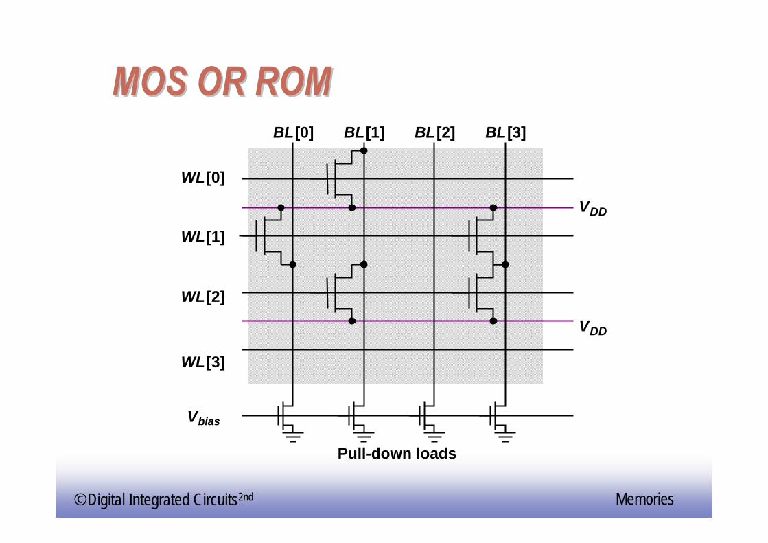
MOS OR ROMMOS OR ROM
WL[0]
VDD
BL[0]
WL[1]
WL[2]
WL[3]
Vbias
BL[1]
Pull-down loads
BL[2] BL[3]
VDD
Page 13
© Digital Integrated Circuits2nd Memories
MOS NOR ROMMOS NOR ROM
WL[0]
GND
BL [0]
WL [1]
WL [2]
WL [3]
VDD
BL [1]
Pull-up devices
BL [2] BL [3]
GND
Page 14
© Digital Integrated Circuits2nd Memories
MOS NOR ROM LayoutMOS NOR ROM Layout
Programmming using theActive Layer Only
Polysilicon
Metal1
Diffusion
Metal1 on Diffusion
Cell (9.5λ x 7λ)
Page 15
© Digital Integrated Circuits2nd Memories
MOS NOR ROM LayoutMOS NOR ROM Layout
Polysilicon
Metal1
Diffusion
Metal1 on Diffusion
Cell (11λ x 7λ)
Programmming usingthe Contact Layer Only
Page 16
© Digital Integrated Circuits2nd Memories
MOS NAND ROMMOS NAND ROM
All word lines high by default with exception of selected row
WL [0]
WL [1]
WL [2]
WL [3]
VDD
Pull-up devices
BL[3]BL[2]BL[1]BL [0]
Page 17
© Digital Integrated Circuits2nd Memories
MOS NAND ROM LayoutMOS NAND ROM Layout
No contact to VDD or GND necessary;
Loss in performance compared to NOR ROMdrastically reduced cell size
Polysilicon
Diffusion
Metal1 on Diffusion
Cell (8λ x 7λ)
Programmming usingthe Metal-1 Layer Only
Page 18
© Digital Integrated Circuits2nd Memories
NAND ROM LayoutNAND ROM LayoutCell (5λ x 6λ)
Polysilicon
Threshold-alteringimplant
Metal1 on Diffusion
Programmming usingImplants Only
Page 19
© Digital Integrated Circuits2nd Memories
Decreasing Word Line DelayDecreasing Word Line Delay
Metal bypass
Polysilicon word lineK cells
Polysilicon word lineWLDriver
(b) Using a metal bypass
(a) Driving the word line from both sides
Metal word line
WL
(c) Use silicides
Page 20
© Digital Integrated Circuits2nd Memories
PrechargedPrecharged MOS NOR ROMMOS NOR ROM
PMOS precharge device can be made as large as necessary,but clock driver becomes harder to design.
WL [0]
GND
BL [0]
WL [1]
WL [2]
WL [3]
VDD
BL [1]
Precharge devices
BL [2] BL [3]
GND
pref
Page 21
© Digital Integrated Circuits2nd Memories
NonNon--Volatile MemoriesVolatile MemoriesThe FloatingThe Floating--gate transistor (FAMOS)gate transistor (FAMOS)
Floating gate
Source
Substrate
Gate
Drain
n+ n+_p
tox
tox
Device cross-section Schematic symbol
G
S
D
Page 22
© Digital Integrated Circuits2nd Memories
FloatingFloating--Gate Transistor ProgrammingGate Transistor Programming
0 V
- 5 V 0 V
DS
Removing programming voltage leaves charge trapped
5 V
- 2.5 V 5 V
DS
Programming results inhigher VT.
20 V
10 V 5 V 20 V
DS
Avalanche injection
Page 23
© Digital Integrated Circuits2nd Memories
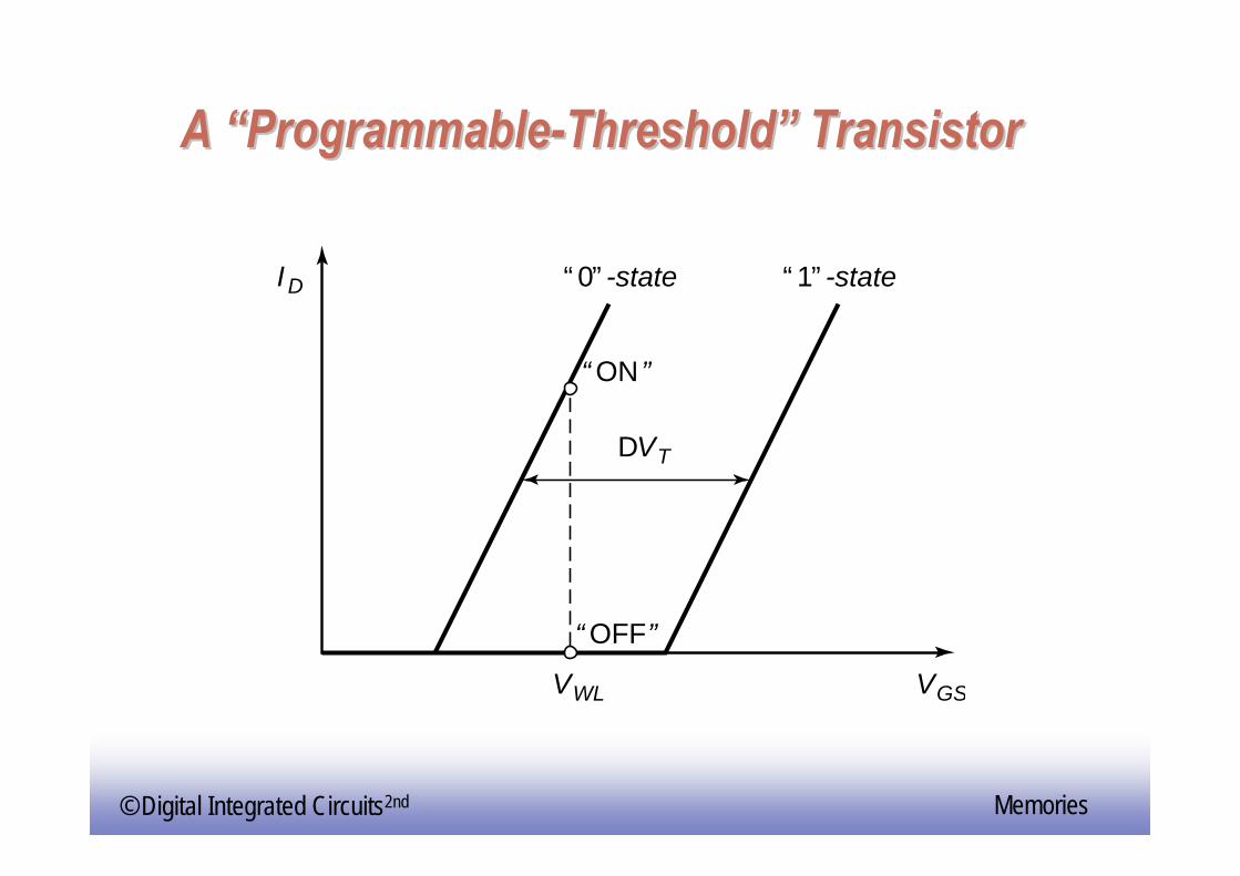
A A ““ProgrammableProgrammable--ThresholdThreshold”” TransistorTransistor
“ 0” -state “ 1” -state
DVT
VWL VGS
“ ON ”
“ OFF”
ID
Page 24
© Digital Integrated Circuits2nd Memories
FLOTOX EEPROMFLOTOX EEPROMFloating gate
Source
Substratep
Gate
Drain
n1 n1
FLOTOX transistor Fowler-NordheimI-V characteristic
20–30 nm
10 nm
-10 V10 V
I
VGD
Page 25
© Digital Integrated Circuits2nd Memories
EEPROM CellEEPROM Cell
WL
BL
VDD
Absolute threshold controlis hardUnprogrammed transistor might be depletion
2 transistor cell
Page 26
© Digital Integrated Circuits2nd Memories
Flash EEPROMFlash EEPROM
Control gate
erasure
p-substrate
Floating gate
Thin tunneling oxide
n1 source n1 drainprogramming
Many other options …
Page 27
© Digital Integrated Circuits2nd Memories
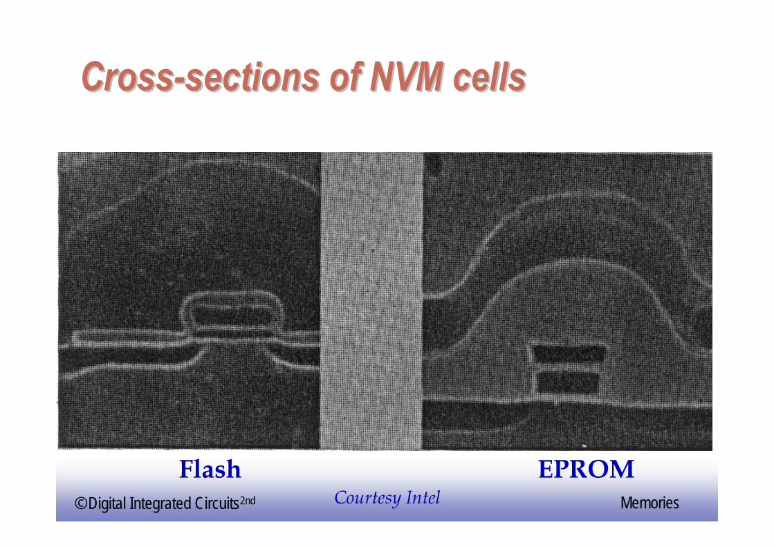
CrossCross--sections of NVM cellssections of NVM cells
EPROMFlashCourtesy Intel
Page 28
© Digital Integrated Circuits2nd Memories
Basic Operations in a NOR Flash MemoryBasic Operations in a NOR Flash Memory――EraseErase
S D
12 VG
cell arrayBL 0 BL 1
open open
WL 0
WL 1
0 V
0 V
12 V
Page 29
© Digital Integrated Circuits2nd Memories
Basic Operations in a NOR Flash MemoryBasic Operations in a NOR Flash Memory――WriteWrite
S D
12 V
6 VG
BL 0 BL 1
6 V 0 V
WL 0
WL 1
12 V
0 V
0 V
Page 30
© Digital Integrated Circuits2nd Memories
Basic Operations in a NOR Flash MemoryBasic Operations in a NOR Flash Memory――ReadRead
5 V
1 VG
S D
BL 0 BL 1
1 V 0 V
WL 0
WL 1
5 V
0 V
0 V
Page 31
© Digital Integrated Circuits2nd Memories
NAND Flash MemoryNAND Flash Memory
Unit Cell
Word line(poly)
Source line(Diff. Layer)
Courtesy Toshiba
GateONO
FGGateOxide
Page 32
© Digital Integrated Circuits2nd Memories
NAND Flash MemoryNAND Flash Memory
Word linesSelect transistor
Bit line contact Source line contact
Active area
STI
Courtesy Toshiba
Page 33
© Digital Integrated Circuits2nd Memories
Characteristics of StateCharacteristics of State--ofof--thethe--art NVMart NVM
Page 34
© Digital Integrated Circuits2nd Memories
ReadRead--Write Memories (RAM)Write Memories (RAM)STATIC (SRAM)
DYNAMIC (DRAM)
Data stored as long as supply is appliedLarge (6 transistors/cell)FastDifferential
Periodic refresh requiredSmall (1-3 transistors/cell)SlowerSingle Ended
Page 35
© Digital Integrated Circuits2nd Memories
66--transistor CMOS SRAM Cell transistor CMOS SRAM Cell
WL
BL
VDD
M5M6
M4
M1
M2
M3
BL
QQ
Page 36
© Digital Integrated Circuits2nd Memories
CMOS SRAM Analysis (Read)CMOS SRAM Analysis (Read)WL
BL
VDD
M 5M 6
M 4
M1 VDDVDD VDD
BL
Q = 1Q = 0
Cbit Cbit
Page 37
© Digital Integrated Circuits2nd Memories
CMOS SRAM Analysis (Read)CMOS SRAM Analysis (Read)
00
0.2
0.4
0.6
0.8
1
1.2
0.5
V o l t a g e r i s e [ V ]
1 1.2 1.5 2Cell Ratio (CR)
2.5 3
Vol
tage
Ris
e (V
)
Page 38
© Digital Integrated Circuits2nd Memories
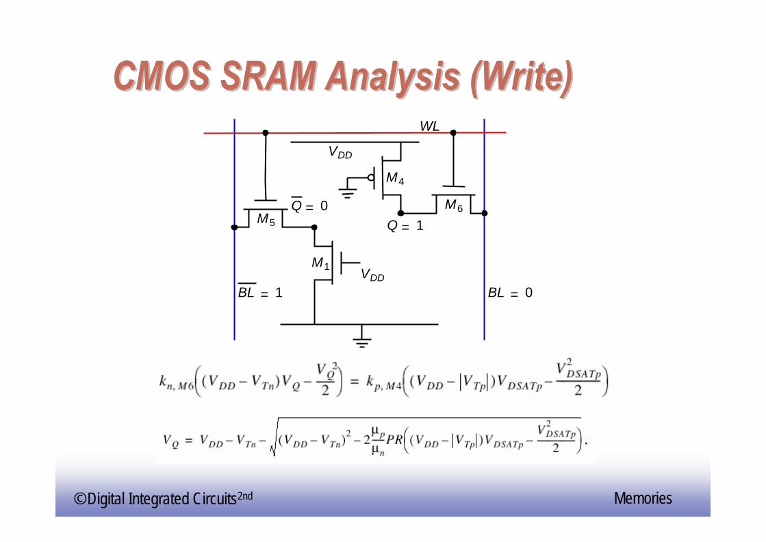
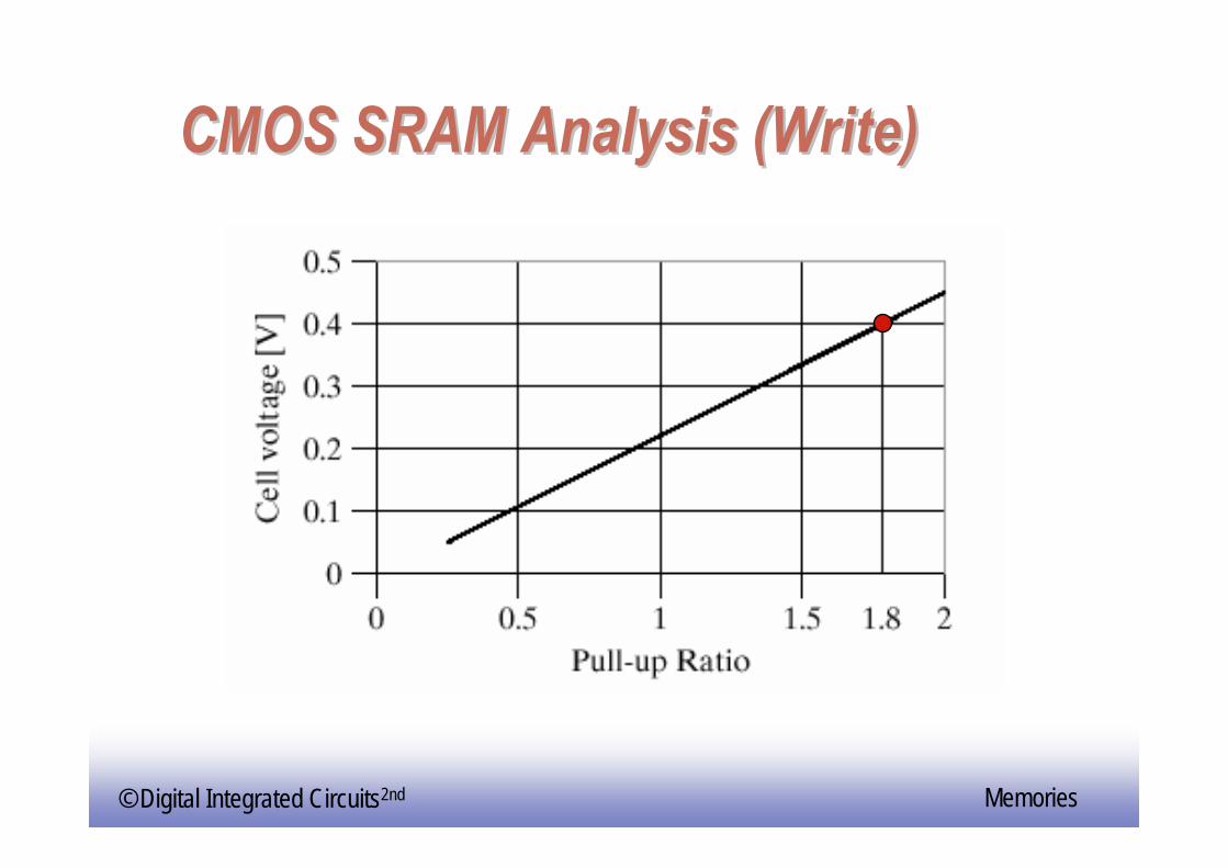
CMOS SRAM Analysis (Write) CMOS SRAM Analysis (Write)
BL = 1 BL = 0
Q = 0Q = 1
M1
M4
M5
M6
VDD
VDD
WL
Page 39
© Digital Integrated Circuits2nd Memories
CMOS SRAM Analysis (Write)CMOS SRAM Analysis (Write)
Page 40
© Digital Integrated Circuits2nd Memories
6T6T--SRAM SRAM —— Layout Layout VDD
GND
QQ
WL
BLBL
M1 M3
M4M2
M5 M6
Page 41
© Digital Integrated Circuits2nd Memories
ResistanceResistance--load SRAM Cellload SRAM Cell
Static power dissipation -- Want RL largeBit lines precharged to VDD to address tp problem
M3
RL RL
VDD
WL
Q Q
M1 M2
M4
BL BL
Page 42
© Digital Integrated Circuits2nd Memories
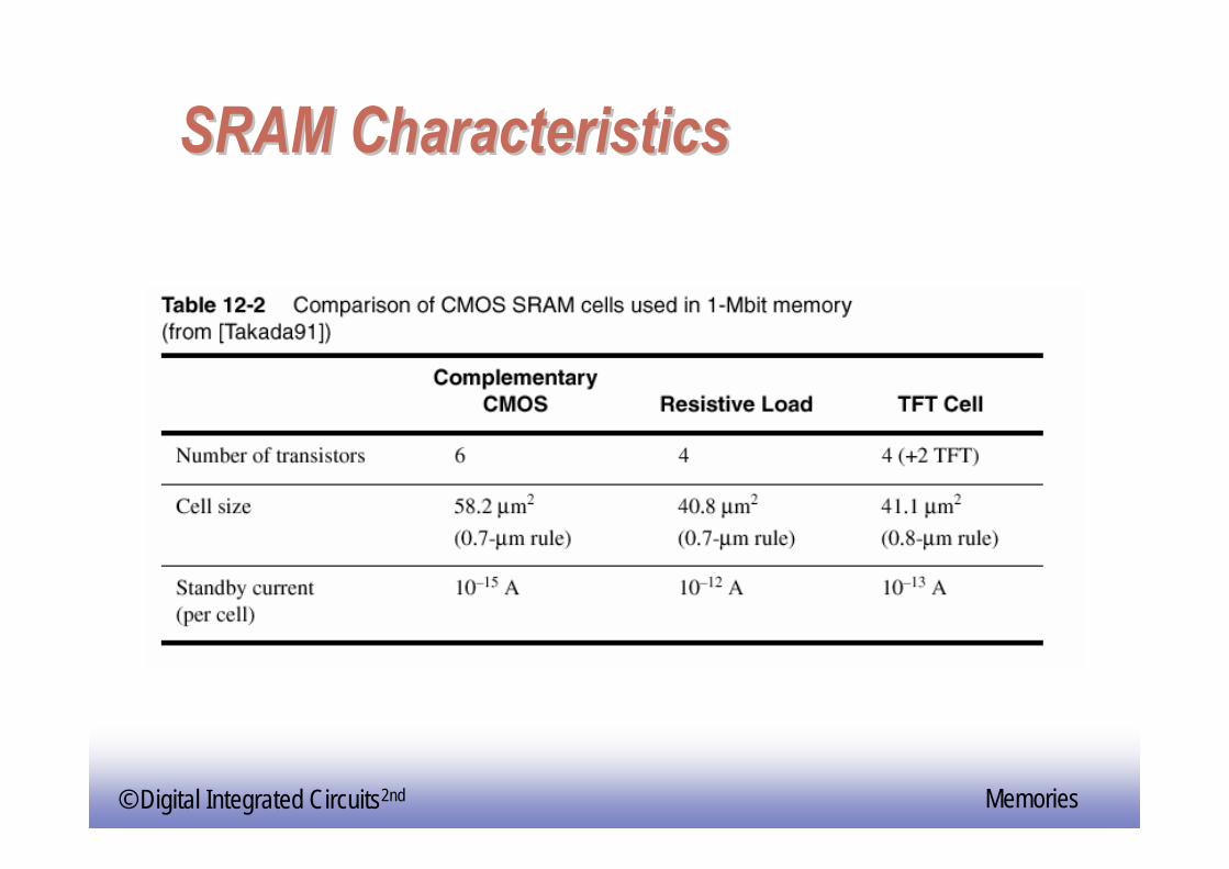
SRAM CharacteristicsSRAM Characteristics
Page 43
© Digital Integrated Circuits2nd Memories
33--Transistor DRAM CellTransistor DRAM Cell
No constraints on device ratiosReads are non-destructiveValue stored at node X when writing a “1” = VWWL-VTn
WWL
BL1
M1 X
M3
M2
CS
BL2
RWL
V DD
VDD 2 VT
DVV DD 2 VTBL 2
BL 1
X
RWL
WWL
Page 44
© Digital Integrated Circuits2nd Memories
3T3T--DRAM DRAM —— LayoutLayout
BL2 BL1 GND
RWL
WWL
M3
M2
M1
Page 45
© Digital Integrated Circuits2nd Memories
11--Transistor DRAM CellTransistor DRAM Cell
Write: CS is charged or discharged by asserting WL and BL.Read: Charge redistribution takes places between bit line and storage capacitance
Voltage swing is small; typically around 250 mV.
M1
CS
WL
BL
CBL
VDD 2 VT
WL
X
sensing
BL
GND
Write 1 Read 1
VDD
VDD /2 VDD /2
ΔV BL VPRE– VBIT VPRE–CS
CS CBL+------------= =V
Page 46
© Digital Integrated Circuits2nd Memories
DRAM Cell ObservationsDRAM Cell Observations1T DRAM requires a sense amplifier for each bit line, due
to charge redistribution read-out.DRAM memory cells are single ended in contrast to
SRAM cells.The read-out of the 1T DRAM cell is destructive; read
and refresh operations are necessary for correct operation.
Unlike 3T cell, 1T cell requires presence of an extra capacitance that must be explicitly included in the design.
When writing a “1” into a DRAM cell, a threshold voltage is lost. This charge loss can be circumvented by bootstrapping the word lines to a higher value than VDD
Page 47
© Digital Integrated Circuits2nd Memories
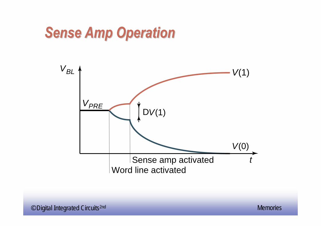
Sense Amp OperationSense Amp Operation
DV(1)
V(1)
V(0)t
VPRE
VBL
Sense amp activatedWord line activated
Page 48
© Digital Integrated Circuits2nd Memories
11--T DRAM CellT DRAM Cell
Uses Polysilicon-Diffusion CapacitanceExpensive in Area
M1 wordline
Diffusedbit line
Polysilicongate
Polysiliconplate
Capacitor
Cross-section Layout
Metal word line
Poly
SiO2
Field Oxiden+ n+
Inversion layerinduced byplate bias
Poly
Page 49
© Digital Integrated Circuits2nd Memories
SEM of polySEM of poly--diffusion capacitor 1Tdiffusion capacitor 1T--DRAMDRAM
Page 50
© Digital Integrated Circuits2nd Memories
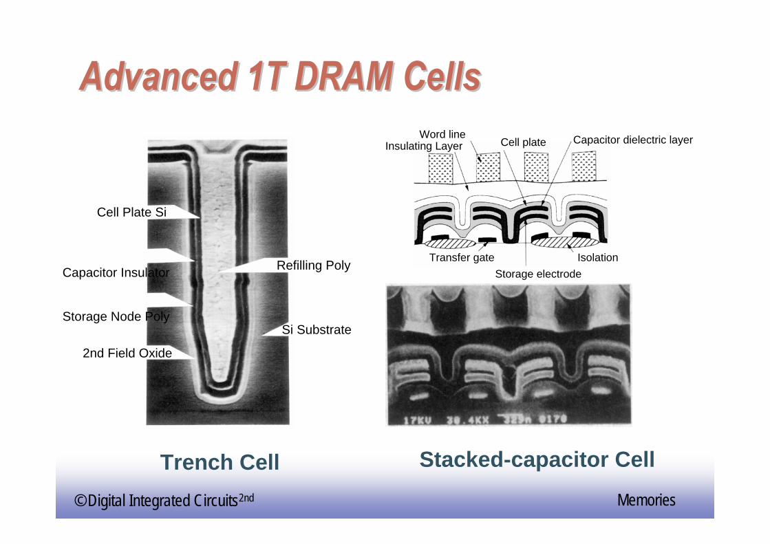
Advanced 1T DRAM CellsAdvanced 1T DRAM Cells
Cell Plate Si
Capacitor Insulator
Storage Node Poly
2nd Field Oxide
Refilling Poly
Si Substrate
Trench Cell Stacked-capacitor Cell
Capacitor dielectric layerCell plateWord line
Insulating Layer
IsolationTransfer gateStorage electrode
Page 51
© Digital Integrated Circuits2nd Memories
Static CAM Memory CellStatic CAM Memory Cell
• • • • • •
CAM
BitWord
Bit
••• CAM
Bit Bit
CAM
Word
Wired-NOR Match Line
Match M1
M2
M7M6
M4 M5M8 M9
M3int
SWord
••• CAM
Bit Bit
S
Page 52
© Digital Integrated Circuits2nd Memories
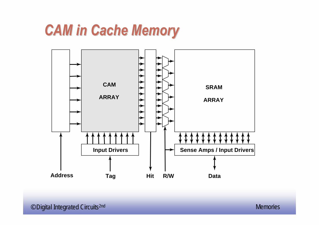
CAM in Cache MemoryCAM in Cache Memory
A d d r e s s D e c o d e r
H i t L o g i c
CAM
ARRAY
Input Drivers
Tag HitAddress
SRAM
ARRAY
Sense Amps / Input Drivers
DataR/W
Page 53
© Digital Integrated Circuits2nd Memories
PeripheryPeriphery
DecodersSense AmplifiersInput/Output BuffersControl / Timing Circuitry
Page 54
© Digital Integrated Circuits2nd Memories
Row DecodersRow DecodersCollection of 2M complex logic gatesOrganized in regular and dense fashion
(N)AND Decoder
NOR Decoder
Page 55
© Digital Integrated Circuits2nd Memories
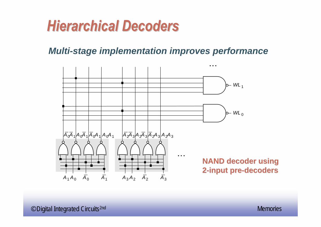
Hierarchical DecodersHierarchical Decoders
• • •
• • •
A2A2
A2A3
WL 0
A2A3A2A3A2A3
A3 A3A0A0
A0A1A0A1A0A1A0A1
A1 A1
WL 1
Multi-stage implementation improves performance
NAND decoder usingNAND decoder using22--input preinput pre--decodersdecoders
Page 56
© Digital Integrated Circuits2nd Memories
Dynamic DecodersDynamic Decoders
Precharge devices
VDD φ
GND
WL3
WL2
WL1
WL0
A0A0
GND
A1A1φ
WL3
A0A0 A1A1
WL 2
WL 1
WL 0
VDD
VDD
VDD
VDD
2-input NOR decoder 2-input NAND decoder
Page 57
© Digital Integrated Circuits2nd Memories
44--input passinput pass--transistor based column transistor based column decoderdecoder
Advantages: speed (tpd does not add to overall memory access time)Only one extra transistor in signal path
Disadvantage: Large transistor count
2 - i n p u t N O R d e c o d e r
A0S0
BL 0 BL 1 BL 2 BL 3
A1
S1
S2
S3
D
Page 58
© Digital Integrated Circuits2nd Memories
44--toto--1 tree based column decoder1 tree based column decoder
Number of devices drastically reducedDelay increases quadratically with # of sections; prohibitive for large decoders
buffersprogressive sizingcombination of tree and pass transistor approaches
Solutions:
BL 0 BL 1 BL 2 BL 3
D
A 0
A 0
A1
A 1
Page 59
© Digital Integrated Circuits2nd Memories
Decoder for circular shiftDecoder for circular shift--registerregister
V DD
V DD
R
WL 0
V DD
f
ff
f
V DD
R
WL 1
V DD
f
ff
f
V DD
R
WL 2
V DD
f
ff
f• • •
Page 60
© Digital Integrated Circuits2nd Memories
Sense AmplifiersSense Amplifiers
tpC ΔV⋅
Iav----------------=
make ΔV as smallas possible
smalllarge
Idea: Use Sense Amplifer
outputinput
s.a.smalltransition
Page 61
© Digital Integrated Circuits2nd Memories
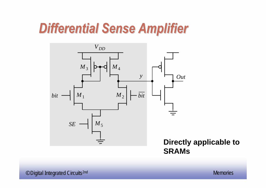
Differential Sense AmplifierDifferential Sense Amplifier
Directly applicable toSRAMs
M 4
M 1
M 5
M 3
M 2
VDD
bitbit
SE
Outy
Page 62
© Digital Integrated Circuits2nd Memories
Differential Sensing Differential Sensing ―― SRAMSRAMVDD
VDD
VDD
VDD
BLEQ
Diff.SenseAmp
(a) SRAM sensing scheme (b) two stage differential amplifier
SRAM cell i
WL i
2xx
VDD
Output
BL
PC
M3
M1
M5
M2
M4
x
SE
SE
SE
Output
SE
x2x 2x
y
y
2y
Page 63
© Digital Integrated Circuits2nd Memories
LatchLatch--Based Sense Amplifier (DRAM)Based Sense Amplifier (DRAM)
Initialized in its meta-stable point with EQOnce adequate voltage gap created, sense amp enabled with SEPositive feedback quickly forces output to a stable operating point.
EQ
VDD
BL BL
SE
SE
Page 64
© Digital Integrated Circuits2nd Memories
Reliability and YieldReliability and Yield
Page 65
© Digital Integrated Circuits2nd Memories
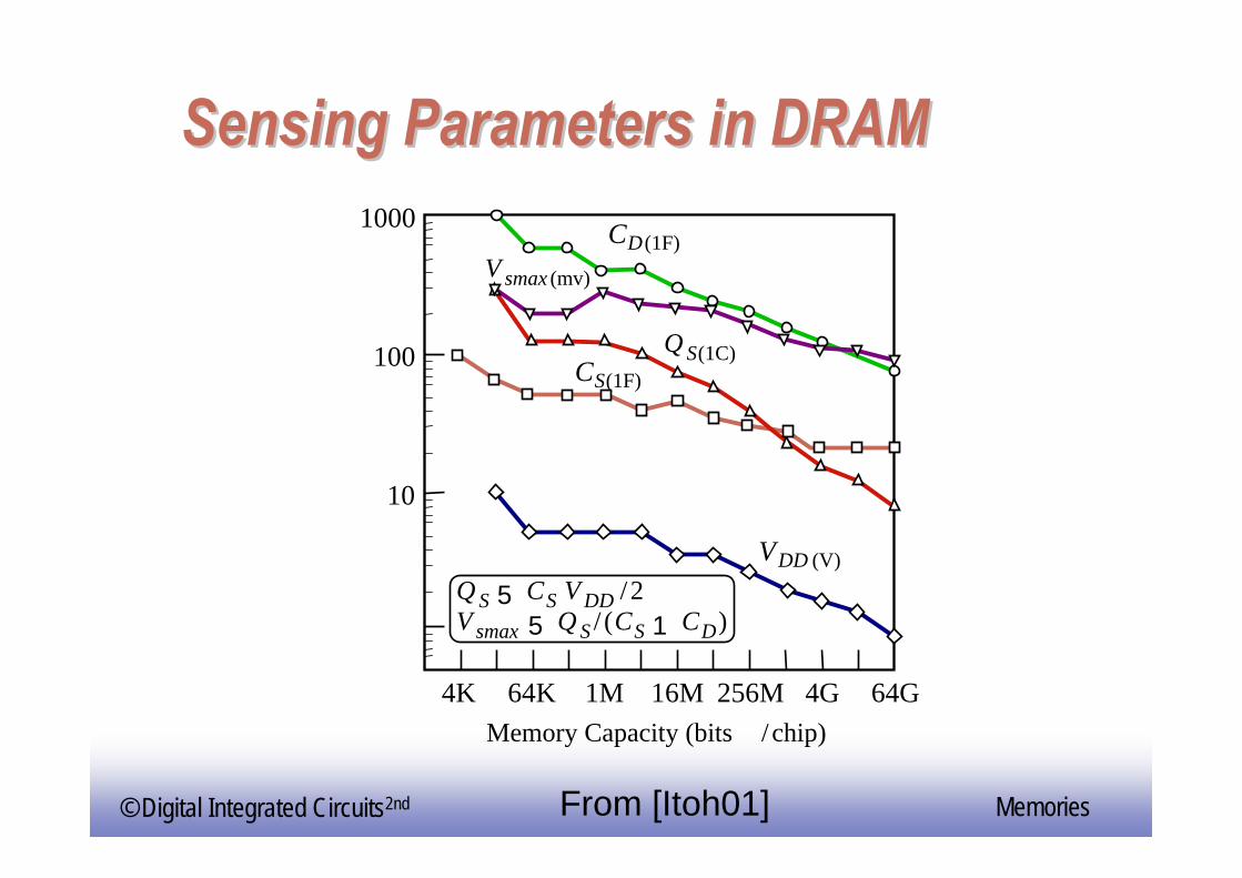
Sensing Parameters in DRAMSensing Parameters in DRAM
From [Itoh01]
4K
10
100
1000
64K 1M 16M 256M 4G 64GMemory Capacity (bits /chip)
C
D
,
Q
S
,
C
S
,
V
D D
,
V
s m a x
CD(1F)
CS(1F)
Q S(1C)
V smax (mv)
VDD (V)Q S 5 CS V DD /2V smax 5 Q S / (CS 1 CD)
Page 66
© Digital Integrated Circuits2nd Memories
Noise Sources in 1T Noise Sources in 1T DRamDRam
Ccross
electrode
a-particles
leakage CS
WL
BL substrate Adjacent BLCWBL
Page 67
© Digital Integrated Circuits2nd Memories
AlphaAlpha--particles (or Neutrons)particles (or Neutrons)
1 Particle ~ 1 Million Carriers
WL
BL
V DD
n1
a-particle
SiO 21
11
11
12
22
22
2
Page 68
© Digital Integrated Circuits2nd Memories
YieldYield
Yield curves at different stages of process maturity(from [Veendrick92])
Page 69
© Digital Integrated Circuits2nd Memories
RedundancyRedundancy
MemoryArray
Column Decoder
R o w D e c o d e r
Redundantrows
Redundantcolumns
RowAddress
ColumnAddress
FuseBank:
Page 70
© Digital Integrated Circuits2nd Memories
ErrorError--Correcting CodesCorrecting CodesExample: Hamming Codes
with
e.g. B3 Wrong
1
1
0
= 3
Page 71
© Digital Integrated Circuits2nd Memories
Redundancy and Error CorrectionRedundancy and Error Correction
Page 72
© Digital Integrated Circuits2nd Memories
Case StudiesCase Studies
Programmable Logic ArraySRAM Flash Memory
Page 73
© Digital Integrated Circuits2nd Memories
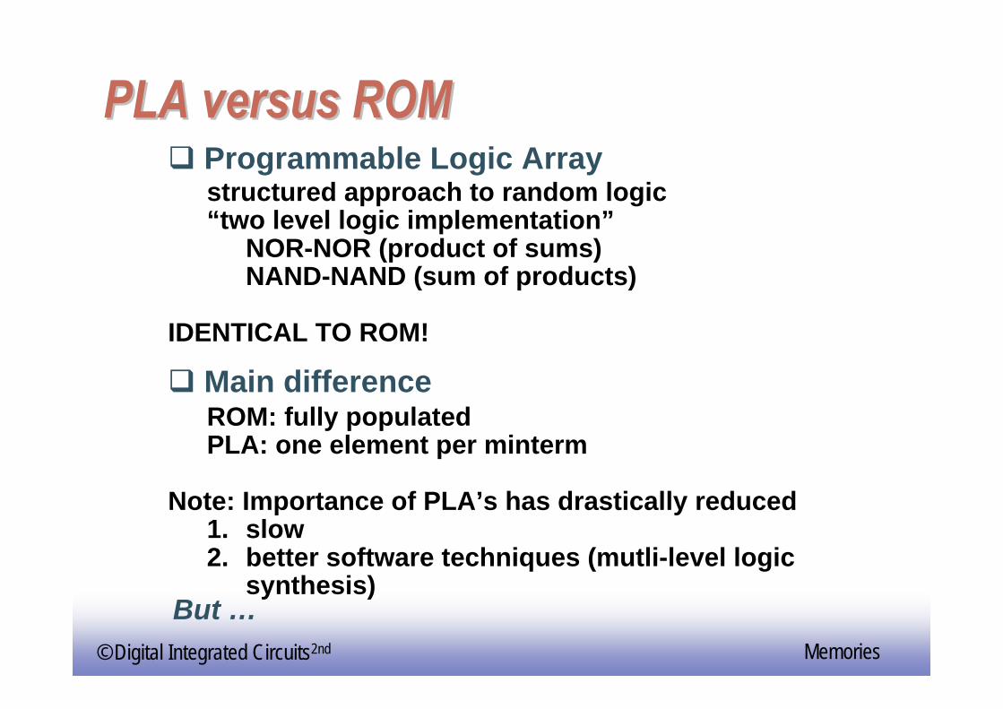
PLA versus ROMPLA versus ROMProgrammable Logic Arraystructured approach to random logic“two level logic implementation”
NOR-NOR (product of sums)NAND-NAND (sum of products)
IDENTICAL TO ROM!
Main differenceROM: fully populatedPLA: one element per minterm
Note: Importance of PLA’s has drastically reduced1. slow2. better software techniques (mutli-level logic
synthesis)But …
Page 74
© Digital Integrated Circuits2nd Memories
Programmable Logic ArrayProgrammable Logic Array
GND GND GND GND
GND
GND
GND
V DD
V DD
X 0X 0 X 1 f0 f1X 1 X 2X 2
AND-plane OR-plane
Pseudo-NMOS PLA
Page 75
© Digital Integrated Circuits2nd Memories
Dynamic PLADynamic PLAGND
GNDVDD
VDD
X 0X 0 X 1 f0 f1X 1 X 2X 2
ANDf
ANDf
ORf
ORf
AND-plane OR-plane
Page 76
© Digital Integrated Circuits2nd Memories
Clock Signal Generation Clock Signal Generation for selffor self--timed dynamic PLAtimed dynamic PLA
f
tpre teval
f AND
f
f AND
f AND
f OR
f OR
(a) Clock signals (b) Timing generation circuitry
Dummy AND row
Dummy AND row
Page 77
© Digital Integrated Circuits2nd Memories
PLA LayoutPLA LayoutVDD GNDφ
And-Plane Or-Plane
f0 f1x0 x0 x1 x1 x2 x2Pull-up devices Pull-up devices
Page 78
© Digital Integrated Circuits2nd Memories
4 4 MbitMbit SRAMSRAMHierarchical WordHierarchical Word--line Architectureline Architecture
Global word line
Sub-global word line
Block groupselect
Blockselect
Blockselect
Memory cell
Localword line
Block 0
•••
Localword line
Block 1
•••
Block 2...
•••
Page 79
© Digital Integrated Circuits2nd Memories
BitBit--line Circuitryline CircuitryBit-lineload
Blockselect ATD
BEQ
Local WL
Memory cell
I/O lineI/O
B /T
CD
Sense amplifier
CD CD
I/O
B /T
Page 80
© Digital Integrated Circuits2nd Memories
Sense Amplifier (and Waveforms)Sense Amplifier (and Waveforms)
BS
I /O I /O
DATA
Blockselect ATD
BSSA SA
BS
SEQ
SEQ
SEQ
SEQSEQ
Dei
I/O Lines
Address
Data-cut
ATD
BEQ
SEQ
DATA
Vdd
GND
SA, SAVdd
GND
Page 81
© Digital Integrated Circuits2nd Memories
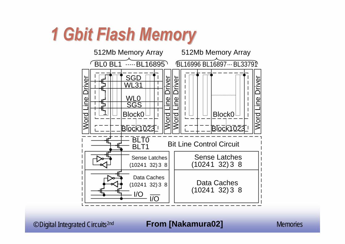
1 1 GbitGbit Flash MemoryFlash Memory
Sense Latches(10241 32) 3 8
Data Caches(10241 32) 3 8
Sense Latches(10241 32) 3 8
Data Caches(10241 32) 3 8
Wor
d Li
ne D
river
Wor
d Li
ne D
river
Wor
d Li
ne D
river
Wor
d Li
ne D
river
512Mb Memory Array 512Mb Memory ArrayBL0 BL1 ····· BL16895 BL16996 BL16897··· BL33791
SGDWL31
WL0SGS
Block0
BLT0Block1023
Block0
Block1023
Bit Line Control CircuitBLT1
I/O I/O
From [Nakamura02]
Page 82
© Digital Integrated Circuits2nd Memories
Writing Flash MemoryWriting Flash MemoryN
umbe
r of m
emor
y ce
lls
0V 1V 2VVt of memory cells
Verify level 5 0.8 V Word-line level 5 4.5 V
3V 4V
Result of 4 timesprogram
R e a d l e v e l ( 4 . 5 V )
N u m b e r o f c e l l s
1000V 1V 2V
Vt of memory cells
3V 4V
102
104
106
108
Evolution of thresholds Final Distribution
From [Nakamura02]
Page 83
© Digital Integrated Circuits2nd Memories
125125mmmm22 1Gbit NAND Flash Memory1Gbit NAND Flash Memory
10.7
mm
11.7mm
2kB
Pag
e bu
ffer &
cac
heC
harg
e pu
mp
16896 bit lines
32 word lines x 1024 blocks
From [Nakamura02]
Page 84
© Digital Integrated Circuits2nd Memories
125125mmmm22 1Gbit NAND Flash Memory1Gbit NAND Flash MemoryTechnology 0.13μm p-sub CMOS triple-well
1poly, 1polycide, 1W, 2AlCell size 0.077μm2Chip size 125.2mm2Organization 2112 x 8b x 64 page x 1k blockPower supply 2.7V-3.6VCycle time 50nsRead time 25μsProgram time 200μs / pageErase time 2ms / block
Technology 0.13μm p-sub CMOS triple-well1poly, 1polycide, 1W, 2Al
Cell size 0.077μm2Chip size 125.2mm2Organization 2112 x 8b x 64 page x 1k blockPower supply 2.7V-3.6VCycle time 50nsRead time 25μsProgram time 200μs / pageErase time 2ms / block
From [Nakamura02]
Page 85
© Digital Integrated Circuits2nd Memories
Semiconductor Memory TrendsSemiconductor Memory Trends(up to the 90(up to the 90’’s)s)
Memory Size as a function of time: x 4 every three years
Page 86
© Digital Integrated Circuits2nd Memories
Semiconductor Memory TrendsSemiconductor Memory Trends(updated)(updated)
From [Itoh01]
Page 87
© Digital Integrated Circuits2nd Memories
Trends in Memory Cell AreaTrends in Memory Cell Area
From [Itoh01]
Page 88
© Digital Integrated Circuits2nd Memories
Semiconductor Memory TrendsSemiconductor Memory Trends
Technology feature size for different SRAM generations