Page 1
JEE-Physics
E:\
Data
\2014\Kota
\JE
E-A
dva
nced
\SM
P\Ph
y\El
ectr
onic
s\Eng
\1. El
ectr
oni
cs-S
emi C
ond
uct
or Th
eory
.p65
E 1
ENERGY BANDS IN SOLIDS
Based on Pauli's exclusion principle
In an isolated atom electrons present in energy level but in solid, atoms are not isolated, there is interaction
among each other, due to this energy level splitted into different energy levels. Quantity of these different
energy levels depends on the quantity of interacting atoms. Splitting of sharp and closely compact energy levels
result into energy bands. They are discrete in nature. Order of energy levels in a band is 1023 and their energy
difference = 10–23 eV.
Energy Band
Range of energy possessed by an electron in a solid is known as energy band.
Valence Band (VB)
Range of energies possessed by valence electron is known as valence band.
(a) Have bonded electrons.
(b) No flow of current due to such electrons.
(c) Always fulfill by electrons.
Conduction Band (CB)
Range of energies possessed by free electron is known as conduction band.
(a) It has conducting electrons.
(b) Current flows due to such electrons.
(c) If conduction band is fully empty then current conduction is not possible.
(d) Electrons may exist or not in it.
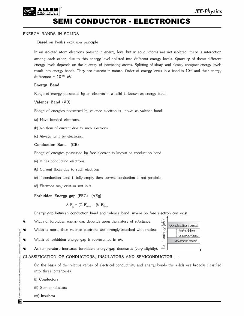
Forbidden Energy gap (FEG) (Eg)
Eg = (C B)
min – (V B)
max
Energy gap between conduction band and valence band, where no free electron can exist.
Width of forbidden energy gap depends upon the nature of substance.
band
en e
rgy
(eV
)
forbiddenenergy gap
conduction band
valence band
Width is more, then valence electrons are strongly attached with nucleus
Width of forbidden energy gap is represented in eV.
As temperature increases forbidden energy gap decreases (very slightly).
CLASSIFICATION OF CONDUCTORS, INSULATORS AND SEMICONDUCTOR : -
On the basis of the relative values of electrical conductivity and energy bands the solids are broadly classified
into three categories
(i) Conductors
(ii) Semiconductors
(iii) Insulator
SEMI CONDUCTOR - ELECTRONICS
Page 2
JEE-Physics
E:\
Data
\2014\Kota
\JE
E-A
dva
nced
\SM
P\Ph
y\El
ectr
onic
s\Eng
\1. El
ectr
oni
cs-S
emi C
ond
uct
or Th
eory
.p65
2 E
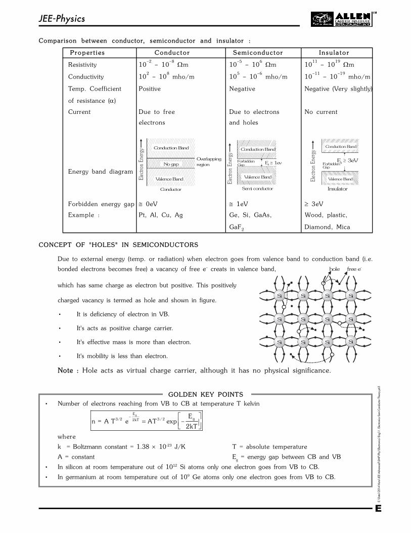
Compar ison between conductor, semiconductor and insu lator :
P roper t i e s Conduc to r Semi condu c to r I n s u l a t o r
Resistivity 10–2
– 10–8
m 10–5
– 106 m 10
11 – 10
19 m
Conductivity 102 – 10
8 mho/m 10
5 – 10
–6 mho/m 10
–11 – 10
–19 mho/m
Temp. Coefficient Positive Negative Negative (Very slightly)
of resistance ()
Current Due to free Due to electrons No current
electrons and holes
Energy band diagram
Overlappingregion
Conductor
Valence Band
No gap
Conduction Band
Elec
tron
Ener
gy
Semi conductor
Elec
tron
Ener
gy
Conduction Band
Valence Band
Forbidden E 1evg Gap
Elec
tron
Ener
gy
ForbiddenGap
Insulator
E 3eVg
Valence Band
Conduction Band
Forbidden energy gap 0eV 1eV 3eV
Example : Pt, Al, Cu, Ag Ge, Si, GaAs, Wood, plastic,
GaF2 Diamond, Mica
CONCEPT OF "HOLES" IN SEMICONDUCTORS
Due to external energy (temp. or radiation) when electron goes from valence band to conduction band (i.e.
bonded electrons becomes free) a vacancy of free e– creats in valence band,
which has same charge as electron but positive. This positively
Si SiSi Si
SiSi Si
SiSi Si Si
Si
hole free e–
charged vacancy is termed as hole and shown in figure.
• It is deficiency of electron in VB.
• It's acts as positive charge carrier.
• It's effective mass is more than electron.
• It's mobility is less than electron.
Note : Hole acts as vir tual charge carrier, although it has no physical significance.
GOLDEN KEY POINTS
• Number of electrons reaching from VB to CB at temperature T kelvin
gE – g3/2 3 / 22kT
En = A T e AT exp –
2kT
where
k = Boltzmann constant = 1.38 10-23 J/K T = absolute temperature
A = constant Eg = energy gap between CB and VB
• In silicon at room temperature out of 1012 Si atoms only one electron goes from VB to CB.
• In germanium at room temperature out of 109 Ge atoms only one electron goes from VB to CB.
Page 3
JEE-Physics
E:\
Data
\2014\Kota
\JE
E-A
dva
nced
\SM
P\Ph
y\El
ectr
onic
s\Eng
\1. El
ectr
oni
cs-S
emi C
ond
uct
or Th
eory
.p65
E 3
EFFECT OF TEMPER ATURE ON SEMICONDUCTOR
At absolute zero kelvin temperature Above absolute temperature
At this temperautre covalent bonds are very With increase in temperature few valence
strong and there are no free electrons and electrons jump into conduction band and hence
semiconductor behaves as perfect insulator. it behaves as poor conductor.
Si SiSi Si
SiSi Si
SiSi Si Si
Si
Conduction band fully empty
Valence band fully filled
at 0 K
Si SiSi Si
SiSi Si
SiSi Si Si
Si
Conduction band partially filled
Valence band partially emptyat high temperature
hole free e–
EFFECT OF IMPURITY IN SEMICONDUCTOR
Doping is a method of addition of "desirable" impurity atoms to pure semiconductor to increase conductivity of
semiconductor. or
Doping is a process of deliberate addition of a desirable impurity atoms to a pure semiconductor to modify its
properties in controlled manner.
Added impurity atoms are called dopants.
The impurity added may be 1 part per million (ppm).
The dopant atom should take the position of semiconductor atom in the lattice.
The presence of the dopant atom should not distort the crystal lattice.
The size of the dopant atom should be almost the same as that of the crystal atom.
The concentration of dopant atoms should not be large (not more than 1% of the crystal atom).
It is to be noted that the doping of a semiconductor increases its electrical conductivity to a great extent.
GOLDEN KEY POINTS
• The concentration of dopant atoms be very low, doping ratio is vary from
impure : pure :: 1 : 106 to 1 : 1010 In general it is 1 : 108
• There are two main method of doping.
(i) Alloy method (ii) Diffusion method (The best)
• The size of dopant atom (impurity) should be almost the same as that of crystal atom. So that crystalline
structure of solid remain unchanged.
CLASSIFICATION OF SEMICONDUCTOR
pentavalent impurity (P, As, Sb etc.)
donar impurity (N )
n >> nD
e h
trivalent impurity (Ga, B, In, Al)
acceptor impurity (N )
n >> nA
h e
Extrinsic semiconductor (doped semicondutor)
(pure form of Ge, Si)n = n = ne h i
N-type P-type
Intrinsic semiconductor
SEMICONDUCTOR
Page 4
JEE-Physics
E:\
Data
\2014\Kota
\JE
E-A
dva
nced
\SM
P\Ph
y\El
ectr
onic
s\Eng
\1. El
ectr
oni
cs-S
emi C
ond
uct
or Th
eory
.p65
4 E
N type semiconductor
When a pure semiconductor (Si or Ge) is doped by pentavalent impurity (P, As, Sb, Bi) then four electrons out
of the five valence electrons of impurity take part, in covalent bonding, with four silicon atoms surrounding it and
the fifth electron is set free. These impurity atoms which donate free e– for conduction are called as Donar
impurity (ND). Due to donar impurity free e– increases very much so it is called as "N" type semiconductor. By
donating e– impurity atoms get positive charge and hence known as "Immobile Donar positive Ion". In N-type
semiconductor free e– are called as "majority" charge carriers and "holes" are called as "minority" charge carriers.
Si SiSi Si
SiSi As
SiSi
Si
N-type semiconducting crystal
As As
donar e–
thermally generated e–
thermally generated hole
free electrons
positive donar ions
N-type semiconductor
minority hole
P type semiconductor
When a pure semiconductor (Si or Ge) is doped by trivalent impurity (B, Al, In, Ga) then outer most three
electrons of the valence band of impurity take part, in covalent bonding with four silicon atoms surrounding it
and except one electron from semiconductor and make hole in semiconductor. These impurity atoms which
accept bonded e– from valance band are called as Acceptor impurity (NA). Here holes increases very much so it
is called as "P" type semiconductor and impurity ions known as "Immobile Acceptor negative Ion". In P-type
semiconductor free e– are called as minority charge carries and holes are called as majority charge carriers.
Si SiSi Si
SiSi
SiSi
Si
P-type semiconducting crystal
Al–
thermally generated e
–
thermally generated hole
Al–
Al–
Extra hole created byacceptor impurity atom
holes
negativeacceptor
ions
P-type semiconductor
minority e
Page 5
JEE-Physics
E:\
Data
\2014\Kota
\JE
E-A
dva
nced
\SM
P\Ph
y\El
ectr
onic
s\Eng
\1. El
ectr
oni
cs-S
emi C
ond
uct
or Th
eory
.p65
E 5
Intr insic Semiconductor N-type (Pentavalent impuri ty ) P-t ype(Tr ivalent impur i t y )
1.
CB
VB
CB
VB
donor impurity level
CB
VB
acceptorimpurity level
2.
free electron
positive donar ion
hole
negativeacceptor
ion
3. Current due to Mainly due to electrons Mainly due to holes
electron and hole
4. ne = n
h = n
in
h << n
e (N
D ~ n
e) n
h >> n
e (N
A ~ n
h)
5. I = Ie + I
hI ~ I
eI ~ I
h
6. Entirely neutral Entirely neutral Entirely neutral
7. Quantity of electrons Majority - Electrons Majority - Holes
and holes are equal Minority - Holes Minority - Electrons
Mass action Law
In semiconductors due to thermal effect, generation of free e– and hole takes place.
Apart from the process of generation, recombination also occurs simultaneously, in which free e– further recombine
with hole.
At equilibrium rate of generation of charge carries is equal to rate of recombination of charge carrier.
The recombination occurs due to e– colliding with a hole, larger value of ne or n
h, higher is the probability of their
recombination.
Hence for a given semiconductor rate of recombination ne × n
h
so rate of recombination = R ne × n
hR = recombination coefficient,
The value of R remains constant for a solid, according to the law of thermodynamics until crystalline lattice
structure remains same.
For intrinsic semiconductor ne = n
h = n
i
so rate of recombination = R ni2
R ne × n
h = R n
i2 n
i2 = n
e × n
h
Under thermal equilibrium, the product of the concentration 'ne' of free electrons and the concentration n
h of
holes is a constant and it is independent of the amount of doping by acceptor and donor impurities.
Thus from mass action law 2e h 1n n n
Page 6
JEE-Physics
E:\
Data
\2014\Kota
\JE
E-A
dva
nced
\SM
P\Ph
y\El
ectr
onic
s\Eng
\1. El
ectr
oni
cs-S
emi C
ond
uct
or Th
eory
.p65
6 E
Electron-hole Recombination :
It is necessarly to complete a bond that electron is shared from neighbouring atoms or it may also be received
from conduction bond. In the second case electron recombines with the hole of valnce bond. This process
is known as electron-hole recombination.
The breaking of bonds or generation of electron-hole pairs, and completion of bonds due to recombination
is taking place continuously.
At equilibrium, the rate of generation becomes equal to the rate of recombination, giving a fixed number
of free electrons and holes.
Ex .1 The energy of a photon of sodium light ( = 589 nm) equals the band gap of a semiconducting material. Find :
(a) the minimum energy E required to create a hole-electron pair.
(b) the value of E
kT at a temperature of 300 K.
So l . (a) E hc
e
(in eV) so
12400E
(E is in eV and is in Å) = 5890 Å
so12400
E 2.1eV5890
(b)19
23
E 2.1 1.6 10 J81
kT 1.38 10 300
Ex .2 A P type semiconductor has acceptor level 57 meV above the valence band. What is maximum wavelength of
light required to create a hole ?
So l .hc
E
hc
E =
34 8
3 19
6.62 10 3 10
57 10 1.6 10
= 217100 Å
Ex .3 A silicon specimen is made into a p-type semiconductor by doping on an average one indium atom per
5 × 10⁷silicon atoms. If the number density of atoms in the silicon specimen is 5 × 1028 atoms/m3; find the
number of acceptor atoms in silicon per cubic centimeter.
So l . The doping of one indium atom in silicon semiconductor will produce one acceptor atom in p-type semiconductor.
Since one indium atom has been dopped per 5 × 10⁷ silicon atoms, so number density of acceptor atoms in
silicon 28
21
7
5 1010
5 10
atom/m3 = = 1015 atoms/cm3
Ex .4 A pure Ge specimen is doped with A. The number density of acceptor atoms is approximately 1021 m–3. If
density of electron holes pair in an intrinsuc semiconductor is approximately 1019m–3, the number density of
electrons in the specimen is :
So l . In pure semiconductor electron-hole pair ni = 1019
m–3
acceptor impurity NA = 1021 m–3
Holes concentration nh = 1021 m–3
electrons concentration = ne =
22 19i
21h
n 10
n 10 = 1017 m–3
Page 7
JEE-Physics
E:\
Data
\2014\Kota
\JE
E-A
dva
nced
\SM
P\Ph
y\El
ectr
onic
s\Eng
\1. El
ectr
oni
cs-S
emi C
ond
uct
or Th
eory
.p65
E 7
Ex .5 Pure Si at 300 K has equal electron (ne) and hole (n
h) concentrations of 1.5 × 10¹⁶ m–3. Dopping by indium
increases nh to 3 × 10²² m–3. Calculate n
e in the doped Si.
So l . For a doped semi-conductor in thermal equilebrium nen
h = n i
2 (Law of mass action)
2 16 2i
e 22h
n (1.5 10 )n
h 3 10
= 7.5 × 10⁹ m–3
RESISTIVITY AND CONDUCTIVITY OF SEMICONDUCTOR
Conduction in conductor
Relation between current (I) and drift velocity (vd )
V
E= V
A
I = ne A vd
n = number of electron in unit volume
A= cross sectional area
current densityI
J = A
amp/m2
= ne vd
drift velocity of electron vd = E
J = ne E J = E
Conductivityne Resistivity
Mobility dv
E
Conduction in Semiconductor
Intr insic semiconductor P - type N - type
ne = n
hn
h >> n
en
e >> n
h
J = ne [ ve + v
h] J e n
h v
hJ e n
e v
e
1
= en [
e +
h ]
1
e nh
h
1
e n
e
e
GOLDEN KEY POINTS
• Due to impurity the conductivity increases approximately 105 times
• sc =
e +
h = n
ee
e + n
h e
h = e(n
eµ
e + n
hµ
h)
Ex .6 What will be conductance of pure silicon crystal at 300K Temp.. If electron hole pairs per cm3 is 1.072 x 10¹⁰
at this Temp, n = 1350 cm2 / volt sec &
P = 480 cm2 / volt sec
So l . = nie
e + n
ie
h= n
ie (
e +
h) = 3.14×10⁻⁶ mho/cm
Ex .7 Pure Si at 300 K has equal electron ne and hole n
h concentration of 1.5 × 10¹⁶/m3. Doping by indium increases
nh to 4.5 × 10²²/m3. Calculate n
e in doped silicon.
So l . ne =
n
nmi
h
2 16 2
22
9 315 10
4 5 105 10
( . )
( . )
Page 8
JEE-Physics
E:\
Data
\2014\Kota
\JE
E-A
dva
nced
\SM
P\Ph
y\El
ectr
onic
s\Eng
\1. El
ectr
oni
cs-S
emi C
ond
uct
or Th
eory
.p65
8 E
Ex .8 A semiconductor has equal electron and hole concentration of 6 × 10⁸/m3. On doping with certain impurity
electron concentration increases to 9 × 10¹²/m3.
(i) Identify the new semiconductor obtained after doping.
(ii) Calculate the new hole concentration.
So l . ni = 6 × 10⁸/m3 and n
e = 9 × 10¹² /m3
(i) ne > n
iso it is N-type semiconductor
(ii) n n ni e h2 n
h =
n
ni
e
2 16
12
36 10
9 10
= 4 × 10⁴ /m3
P - N JUNCTION
Techniques for making P-N junct ion
(i) Alloy Method or Alloy Junction
Here a small piece of III group impurity like indium is placed over n–Ge or n–Si and melted as shown in figure
ultimetely P – N junction form.
N-type N-type N-type
indium indiumindium buttom
liquidPN J
n
P-type P-type P-type
arsenic buttomliquidarsenic arsenic
PN Jn
(ii) Diffusion Junction
A heated P–type semiconductor is kept in pentavalent N-type Ge/Sivacuum
to vacuum pump
Al vapours
heat
diffused P-type layer
P-N Jn
impurity vapours which diffuse into P–type semiconductor as
shown and make P–N junction.
(iii) Vapour deposited junction or epitaxial junction
If we want to grow a layer of n–Si or p–Si then p–Si wafer is
kept in an atmosphere of Silane (a silicon compound which
dissociates into Si at high temperatures) plus phosphorous
vapours. On craking of silane at high temperature a fresh layer on n–Si grows on p–Si giving the "P–N
junction". Since this junction growth is layer by so it is also referred as layer growth or epitaxial junction formation
of P–N junction.
Descr iption of P-N Junction without applied voltage or bias
Given diagram shows a P–N junction immediately after it is formed.
P region has mobile majority holes and immobile negatively
charged impurity ions.
p n
hole free electron
– +
+
–distance
distance
distance
V = Potential
barrier0El
ectri
c Po
tent
ial
deplition layer
width (10)-6
char
gede
nsity
elec
tric
fie
ldin
tens
ity
N region has mobile majority free electrons and immobile positively
charged impurity ions.
Due to concentration difference diffusion of holes starts from P to N
side and diffusion of e– s starts N to P side.
Due to this a layer of only positive (in N side) and negative
(in P–side) started to form which generate an electric field (N to P
side) which oppose diffusion process, during diffusion magnitude of
electric field increases due to this diffusion it gradually decreased
and ultimately stopes.
The layer of immobile positive and negative ions, which have no
free electrons and holes called as depletion layer as shown in
diagram.
Page 9
JEE-Physics
E:\
Data
\2014\Kota
\JE
E-A
dva
nced
\SM
P\Ph
y\El
ectr
onic
s\Eng
\1. El
ectr
oni
cs-S
emi C
ond
uct
or Th
eory
.p65
E 9
GOLDEN KEY POINTS
• Width of depletion layer 10-6 m
(a) As doping increases depletion layer decreases
(b) As temperature is increased depletion layer also increases.
(c) P-N junction unohmic, due to nonlinear relation between I and V.
• Potential Barr ier or contact potential
G e 0.3 V Si 0.7 V
• Electric field, produce due to potential barrier 6
V 0.5E
d 10 E 105 V/m
This field prevents the respective majority carrier from crossing barrier region
DIFFUSION AND DRIFT CURRENT
(1) Diffusion current – P to N side (2) Drift current – N to P side
If there is no biasing diffusion current = drift current
So total current is zero
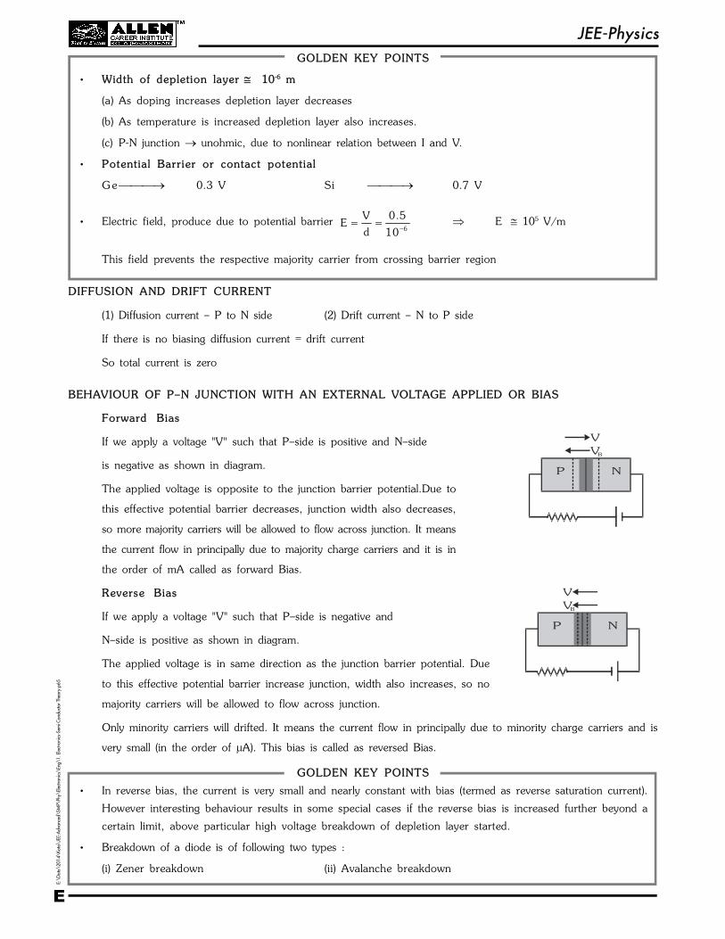
BEHAVIOUR OF P–N JUNCTION WITH AN EXTERNAL VOLTAGE APPLIED OR BIAS
Forward Bias
If we apply a voltage "V" such that P–side is positive and N–side VVB
P Nis negative as shown in diagram.
The applied voltage is opposite to the junction barrier potential.Due to
this effective potential barrier decreases, junction width also decreases,
so more majority carriers will be allowed to flow across junction. It means
the current flow in principally due to majority charge carriers and it is in
the order of mA called as forward Bias.
Reverse Bias
If we apply a voltage "V" such that P–side is negative and
VVB
P N
N–side is positive as shown in diagram.
The applied voltage is in same direction as the junction barrier potential. Due
to this effective potential barrier increase junction, width also increases, so no
majority carriers will be allowed to flow across junction.
Only minority carriers will drifted. It means the current flow in principally due to minority charge carriers and is
very small (in the order of µA). This bias is called as reversed Bias.
GOLDEN KEY POINTS
• In reverse bias, the current is very small and nearly constant with bias (termed as reverse saturation current).
However interesting behaviour results in some special cases if the reverse bias is increased further beyond a
certain limit, above particular high voltage breakdown of depletion layer started.
• Breakdown of a diode is of following two types :
(i) Zener breakdown (ii) Avalanche breakdown
Page 10
JEE-Physics
E:\
Data
\2014\Kota
\JE
E-A
dva
nced
\SM
P\Ph
y\El
ectr
onic
s\Eng
\1. El
ectr
oni
cs-S
emi C
ond
uct
or Th
eory
.p65
10 E
Comparison between Forward Bias and Reverse Bias
Forward Bias Reverse Bias
P
N negative
positive P
N positive
negative
P N
V
+ –
P N
V
+–
1. Potential Barrier reduces 1. Potential Barrier increases.
2. Width of depletion layer decreases 2. Width of depletion layer increases.
3. P-N jn. provide very small resistance 3. P-N jn. provide high resistance
4 Forward current flows in the circuit 4 . Very small current flows.
5. Order of forward current is milli ampere. 5. Order of current is micro ampere for Ge
or Neno ampere for Si.
6 . Current flows mainly due to majority carriers. 6 . Current flows mainly due to minority carriers.
7 . Forward characteristic curves. 7. Reverse characteristic curve
0
if(mA)
V(volt)f
knee voltage
break downvoltage
V(volt)r
Ir ( A)
Reverse saturationcurrent
8. Forward resistance 8. Reverse resistance
ff
f
VR 100
I
6rr
r
VR 10
I
9. Order of knee or cut in voltage 9. Breakdown voltage
G e 0.3 V G e 25 V
Si 0.7 V Si 35 V
Special point : Generally 3r
f
R = 10 : 1 for Ge
R4r
f
R = 10 : 1 for Si
R
Page 11
JEE-Physics
E:\
Data
\2014\Kota
\JE
E-A
dva
nced
\SM
P\Ph
y\El
ectr
onic
s\Eng
\1. El
ectr
oni
cs-S
emi C
ond
uct
or Th
eory
.p65
E 11
Ex .9 The resistance of p-n junction diode decreases when forward biased and increases when reverse biased.
Why?
So l . When p-n junction is forward biased, the width of depletion layer decreases and the barrier potential is opposed
by the forward bias. In other words, potential barrier decreases. Hence the diffusion of holes and electrons
through the junction increases. Due to this, the diode current increases and hence resistance decreases.
When p-n junction is reverse biased, the barrier potential is supported and the width of depletion layer increases.
As a result of this, the diode current becomes almost zero as there is no diffusion of majority carriers (electrons
and holes) through the junction. Hence the resistance of the junction diode increases when reverse biased.
Ex.10 What is an ideal diode ? Draw the output waveform across the load resistor R, if the input waveform is
as shown in the figure.
+6V
V
-6V
So l . An ideal diode has zero resistance when forward biased and infiniter resistance when it is reversed biased.
Output wave form is shown in fig.
+6V
0V
Ex.11A potential barrier of 0.5 V exists across a p-n junction (i) If the depletion region is 5 × 10⁻⁷ m wide. What is the
intensity of the electric field in this region ? (ii) An electron with speed 5×10⁵ m/s approaches the p-n
junction from the n-side with what speed will it enter the p-side.
So l . : (i) Width of depletion layer L = 5 × 10⁻⁷ m
7
V 0.5VE
L 5 10
= 106 volt/m P N
E=VL
(ii) Work energy theorm 2 2i f
1 1Mv eV Mv
2 2
2i
f
Mv 2eVv
M
= 2.7 × 10⁵ m/s
Ex.12 Figure shows a diode connected to an external resistance and an e.m.f. Assuming that the barrier potential
developed in diode is 0.5 V1 obtain the value of current in the circuit in milliampere.
So l . E = 45 V1R = 100
voltage drop across p-n junction = 0.5 V
effective voltage in the circuit V = 4.5 – 0.5 = 4.0 V4.5V
100
current in the circuit V 4.0
I 0.04AR 100
= 0.04 × 1000 mA = 40mA
Ex.13Differentiate zener and avalanche breakdown.
So l . The difference between these two are as follows
Page 12
JEE-Physics
E:\
Data
\2014\Kota
\JE
E-A
dva
nced
\SM
P\Ph
y\El
ectr
onic
s\Eng
\1. El
ectr
oni
cs-S
emi C
ond
uct
or Th
eory
.p65
12 E
Zener Break down Avalanche Break down
Where covalent bonds of depletion layer, its Here covalent bonds of depletion layers are bro
self break, due to high electric field of very ken by collision of "Minorities" which aquire
high Reverse bias voltage. high kinetic energy from high electric field of
very-very high reverse bias voltage.
This phenomena predominant This phenomena predominant
(i) At lower voltage after "break down" (i) At high voltage after breakdown
(ii) In P – N having "High doping" (ii) In P – N having "Low doping"
(iii) P – N Jn. having thin depletion layer (iii) P – N Jn. having thick depletion layer
Here P – N not demage paramanently Here P – N damage peramanentaly due to
"In D.C voltage stablizer zener phenomenan "Heating effect" due to abruptly increament of
is used". minorities during repeatative collisoins.
CHARACTERISTIC CURVE OF P-N JUNCTION DIODE
P NP N
symbol
Forward bias Reverse bias
Reversebias curve
D D+
+
– Rh Rh
R R
(0-1)V (0-10)V+ –
mA A–
Forward bias curveI
mA
f
IA
r
Vf
Vr
O (Volt)
(Volt)(
)
()
In forward bias when voltage is increased from 0V is steps and corresponding value of current is measured, the
curve comes as OB of figure. We may note that current increase very sharply after a certain voltage knee
voltage. At this voltage, barrier potential is completely eliminated and diode offers a low resistance.
In reverse bias a microammeter has been used as current is very very small. When reverse voltage is increased
from 0V and corresponding values of current measured the plot comes as OCD. We may note that reverse
current is almost constant hence called reverse saturation current. It implies that diode resistance is very high. As
reverse voltage reaches value VB, called breakdown voltage, current increases very sharply.
For Ideal Diode
'ON' switch
in forward bias
R = 0 f
'OFF' switch
in reverse bias
R = r
RECTIF IER
It is device which is used for converting alternating current into direct current.
Page 13
JEE-Physics
E:\
Data
\2014\Kota
\JE
E-A
dva
nced
\SM
P\Ph
y\El
ectr
onic
s\Eng
\1. El
ectr
oni
cs-S
emi C
ond
uct
or Th
eory
.p65
E 13
Half wave recti f ier
S1
S2
D A
RL
B
S1 DA
RL
B
Input
OutputS2
For negative half cycleFor positive half cycle
A.C. Supply
Secondry Voltage
A.C. Supply
During the first half (positive) of the input signal, let S1 is at positive and S
2 is at negative potential. So, the PN
junction diode D is forward biased. The current flows through the load resistance RL and output voltage is
obtained.
During the second half (negative) of the input signal, S1 and S
2 would be negative and positive respectively. The
PN junction diode will be reversed biased. In this case, practically no current would flow through the load
resistance. So, there will be no output voltage.
Thus, corresponding to an alternating input signal, we get a unidirectional pulsating output as shown.
Peak inverse voltage (PIV)
In half wave rectifier PIV = maximum voltage across secondary coil of transformer (Vs)
= Peak value of output (Vm)
Ful l wave recti f ier
When the diode rectifies the whole of the AC wave, it is called full wave rectifier. Figure shows the experiemental
arrangement for using diode as full wave rectifier. The alternating signal is fed to the primary a transformer. The
output signal appears across the load resistance RL.
D2
S2
RL
AB
D1
Input
Output
S1
D1 D1 D1 D1D2 D2 D2
For positive half cycle
A. C. Supply
For negative half cycle
D1
A
RL
D2
S1
S2
BA. C. Supply
Secondry Voltage
During the positive half of the input signal :
Let S1 positive and S
2 negative.
In this case diode D1 is forward biased and D
2 is reverse biased. So only D
1 conducts and hence the flow of
current in the load resistance RL is from A to B.
During the negative half of the input signal :
Now S1 is negative and S
2 is positive. So D
1 is reverse-biased and D
2 is forward biased. So only D
2 conducts and
hence the current flows through the load resistance RL from A to B.
It is clear that whether the input signal is positive or negative, the current always flows through the load resistance
in the same direction and full wave rectification is obtained.
Page 14
JEE-Physics
E:\
Data
\2014\Kota
\JE
E-A
dva
nced
\SM
P\Ph
y\El
ectr
onic
s\Eng
\1. El
ectr
oni
cs-S
emi C
ond
uct
or Th
eory
.p65
14 E
Bridge Recti f ier
D3
D1 Input
Output
D2
D4
RL
D1,D4 D2,D3 D1,D4 D2,D3 D1,D4
During posi t ive half cycle During negative half cycle
D1 and D
4 are forward biased on switch D
2 and D
3 are forward biased on switch
D2 and D
3 are reverse biased off switch D
1 and D
4 are reverse biased offswitch
In bridge rectifier peak inverse voltage PIV = Vs = V
m
Form Factor
F = rms
dc
I
I orrms
dc
E
E
for full wave rectifier F = 2 2
for half wave rectifier F =
2
Ripple and r ipple factor
In the output of rectifier some A.C. components are present. They are called ripple & there measurement is given
by a factor known as ripple factor. For a good rectifier ripple factor must be very low.
Total output current
Irms
= 2 2ac dcI + I Where I
ac = rms value of AC component present in output
Ripple factor r = ac
dc
I
I r =
2rms
2dc
I1
I = 2F 1
Recti f ier eff ic iency
2dc dc L
2ac rms F L
P I R = =
P I (R + R )
Half wave recti f ier Full wave rectif ier or br idge wave rectif ier
f
L
0.406 =
R1
R
f
L
0.812
R1
R
If f
L
R < < 1
R , then = 40.6% If f
L
R < < 1
R , then 81.2%
Special Note If Rf = R
LSpecial Note If R
f = R
L
20.3% 40.6%
Note : In brige full wave rectifier Rf is two times of resistance of P-N jn. diode in FB.
Page 15
JEE-Physics
E:\
Data
\2014\Kota
\JE
E-A
dva
nced
\SM
P\Ph
y\El
ectr
onic
s\Eng
\1. El
ectr
oni
cs-S
emi C
ond
uct
or Th
eory
.p65
E 15
Ripple Frequency
( i ) For half wave recti f ier
input frequency = 50Hz ripple frequency = 50Hz
input output
( i i ) for ful l wave recti f ier
input frequency = 50Hz ripple frequency = 100Hz
input output
P u l s e
( i ) For half wave recti f ier
input output
Pulse frequency = 100 Hz Pulse frequency = 50 Hz
( i i ) For fu l l wave rectif ier
input output
Pulse frequency = 100 Hz Pulse frequency = 100 Hz
Comparison Between Average Recti f iers
Fu l l -wave
Hal f -wave Centre - tap B r i d g e
Number of Diodes 1 2 4
Transformer necessary No Yes No
Peak secondary voltage Vs
Vs
Vs
Peak Inverse Voltage Vs = V
mV
s = 2V
mV
s = V
m
(when peak of output = Vm)
Peak load Current, Im
in
d L
V
r Rin
d L
V
r Rin
d L
V
2r R
RMS Current, Irms
mI
2
mI
2
mI
2
DC current, Idc
mI
m2 I
m2 I
Ripple factor, r 1.21 0.482 0.482
Rectification efficiency (max) 40.6% 81.2% 81.2%
Ripple frequency (when input = 50 Hz) 50 Hz 100 Hz 100 Hz
Page 16
JEE-Physics
E:\
Data
\2014\Kota
\JE
E-A
dva
nced
\SM
P\Ph
y\El
ectr
onic
s\Eng
\1. El
ectr
oni
cs-S
emi C
ond
uct
or Th
eory
.p65
16 E
Ex .14 A sinusoidal voltage of amplitude 25 volts and frequency 50 Hz is applied to a half wave rectifier using
PN diode. No fi lter is used and the load resistor is 1000 . The forward resistance Rf ideal diode is
10 . Calculate
(i) Peak, average and rms values of load currrent.
(ii) d.c. power output (iii) a.c. power input
(iv) % Rectifier efficiency (v) Ripple factor
So l . (i)m
m
f L
V 25
R R (10 1000)
= 24.75 mA
mdc
24.757.88mA
3.14
mrms
24.7512.38mA
2 2
(ii) Pdc = Idc
2 × RL = (7.88 × 10
–3)2 × 10
3 62 mW
(iii) Pac = Irms
2(Rf + RL) = (12.38 × 10
–3)2 × (10 + 1000)
155 mW
(iv) Rectifier efficiency = dc
ac
P
P × 100
= 62
155 × 100 = 40 %
(v) Ripple factor = I
I
1 / 22
rms
ac
1
=
212.38
17.88
= 1.21
Ex.15 The halfwave rectifier supplies power to a 1 k load. The input supply voltage is 220 V neglecting forward
resistance of the diode, calculate
(i) Vdc
(ii) dc and
(iii) Ripple voltage (rms value)
So l . (i) m rmsdc
V 2 V 2 220V 99
3.14
volt
(ii)dc
dc
L
V 9999 mA
R 1000
(iii) r = r rms
dc
(V )
V
or (Vr)rms = r × vdc = 1.21 × 99 = 119.79 volt.
Ex.16 A fullwave rectifier supplies a load of 1 K. The a.c. voltage applied to the diodes is 220 volt rms. If
diode resistance is neglected, calculate.
(i) Average d.c. voltage (ii) Average d.c. current (iii) Ripple voltage (rms)
So l . (i) Average d.c. voltage Vdc =m2V
= 0.636 Vm
where Vm = maximum across each half of the secondary winding.
If V be the rms voltage across each half of the secondary winding then mVV
2
Vdc = 0.636 × V 2 = 0.9 V = 0.9 × 220 = 198 volt.
(ii) For fullwave rectifier Idc = dc
L
V
R =198
1000= 198 mA
(iii) r = r ( rms )
dc
V
V Vr(rms) = r × Vdc Vr(rms) = 0.482 × 198 = 95.436 volt
Page 17
JEE-Physics
E:\
Data
\2014\Kota
\JE
E-A
dva
nced
\SM
P\Ph
y\El
ectr
onic
s\Eng
\1. El
ectr
oni
cs-S
emi C
ond
uct
or Th
eory
.p65
E 17
Ex.17 A fullwave P.N. diode rectifier used load ressitor of 1500 . No filter is used. Assume each diode to have
idealized charcteristic with Rf = 10 and Rr = . Since wave voltage applied to each diode has amplitude
of 30 volts and frequency 50Hz. Calculate.
(i) Peak, d.c. rms load current
(ii) d.c. power input
(iii) A.C. power input
(iv) Rectifier efficiency
So l . (i) Peak current Im = m
f L
V
R R
Im = 30volts
10 1500 = 19.9 mA
d.c. load current Idc = 2Im
= 0.636 Im= 0.636 × 19.9 mA = 12.66 mA.
rms = m 19.9
14 mA2 2
(ii) D.C. Power output Pdc = Idc
2 × RL
= (12.66 × 10⁻³
)2 × 1500 Watt = 240.41 mW
(iii) A.C. power input Pin = Irms
2 (Rf + R2)
= (14 × 10–3
)2 (10 + 1500) watt = 295.96 mW
FILTER CIRCUIT
To reduce A.C. Components
Capacitor Fi l ter
DC
RLACoutput of rectifier
AC + DC
outputC
L - C FilterDC
RLACoutput of rectifier
AC + DC
outputC
DC + low AC
- Fil ter (Best Fi lter)
DC
AC RLACoutput of rectifier
AC + DC
outputapprox pure D.C
C2C1
DC + low AC
Page 18
JEE-Physics
E:\
Data
\2014\Kota
\JE
E-A
dva
nced
\SM
P\Ph
y\El
ectr
onic
s\Eng
\1. El
ectr
oni
cs-S
emi C
ond
uct
or Th
eory
.p65
18 E
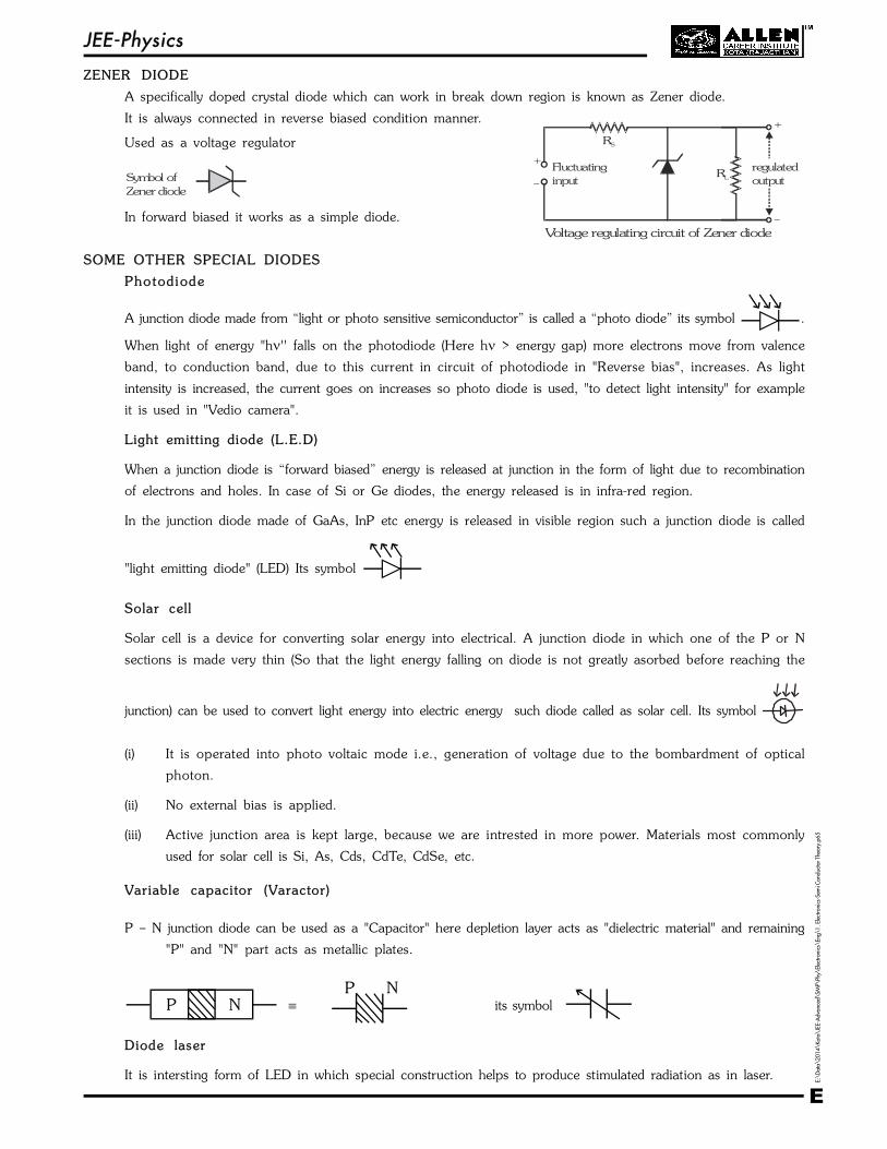
ZENER DIODE
A specifically doped crystal diode which can work in break down region is known as Zener diode.
It is always connected in reverse biased condition manner.
regulated output
RL
Fluctuatinginput
+
+
RS
Voltage regulating circuit of Zener diode
Used as a voltage regulator
Symbol of Zener diode
In forward biased it works as a simple diode.
SOME OTHER SPECIAL DIODES
Photod iode
A junction diode made from “light or photo sensitive semiconductor” is called a “photo diode” its symbol .
When light of energy "h'' falls on the photodiode (Here h > energy gap) more electrons move from valence
band, to conduction band, due to this current in circuit of photodiode in "Reverse bias", increases. As light
intensity is increased, the current goes on increases so photo diode is used, "to detect light intensity" for example
it is used in "Vedio camera".
Light emitt ing diode (L.E.D)
When a junction diode is “forward biased” energy is released at junction in the form of light due to recombination
of electrons and holes. In case of Si or Ge diodes, the energy released is in infra-red region.
In the junction diode made of GaAs, InP etc energy is released in visible region such a junction diode is called
"light emitting diode" (LED) Its symbol
Solar cel l
Solar cell is a device for converting solar energy into electrical. A junction diode in which one of the P or N
sections is made very thin (So that the light energy falling on diode is not greatly asorbed before reaching the
junction) can be used to convert light energy into electric energy such diode called as solar cell. Its symbol
(i) It is operated into photo voltaic mode i.e., generation of voltage due to the bombardment of optical
photon.
(ii) No external bias is applied.
(iii) Active junction area is kept large, because we are intrested in more power. Materials most commonly
used for solar cell is Si, As, Cds, CdTe, CdSe, etc.
Var iable capaci tor (Varactor)
P – N junction diode can be used as a "Capacitor" here depletion layer acts as "dielectric material" and remaining
"P" and "N" part acts as metallic plates.
its symbol
Diode laser
It is intersting form of LED in which special construction helps to produce stimulated radiation as in laser.
Page 19
JEE-Physics
E:\
Data
\2014\Kota
\JE
E-A
dva
nced
\SM
P\Ph
y\El
ectr
onic
s\Eng
\1. El
ectr
oni
cs-S
emi C
ond
uct
or Th
eory
.p65
E 19
Ex .18 A zener diode of voltage VZ (=6V) is used to maintain a constant voltage across a load resistance RL (=1000)
by using a series resistance RS (=100). If the e.m.f. of source is E (= 9 V), calculate the value of current
through series resistance, Zener diode and load resistance. What is the power being dissipated in Zener
diode.
So l . Here, E = 9V ; VZ = 6V ; RL = 1000 and RS = 100,
Potential drop across series resistor VR = E – VZ = 9 – 6 = 3 V
Current through series resistance RS is RV 30.03A
R 100
Current through load resistance RL is ZL
L
V 60.006A
R 1000
Current through Zener diode is IZ = I - IL = 0.03 - 0.006 = 0.024 amp.
Power dissipated in Zener diode is PZ = VZ IZ = 6 x 0.024 = 0.144 Watt
Ex.19 A Zener diode is specified having a breakdown voltage of 9.1 V with a maximum power dissipation of
364 mW. What is the maximum current that the diode can handle.
So l . Maximum current that the given diode can handle is 3364 10
9.1
A i.e., 40 mA.
TRANSISTOR
Inventor William Bradford Shockley, John Bardeen and Walter Houser Brattain.
Transistor is a three terminal device which transfers a singal from low resistance circuit to high resistance circuit.
It is formed when a thin layer of one type of extrinsic semiconductor (P or N type) is sandwitched between two
thick layers of other type of extrinsic semiconductor.
Each transistor have three terminals which are :-
(i) Emitter
(ii) Base
(iii) Collector
Emitter : It is the left most part of the transistor. It emit the majority carrier towards base. It is highly doped and
medium in size.
Base : It is the middle part of transistor which is sandwitched by emitter (E) and collector (C). It is lightly doped
and very thin in size.
Collector : It is right part of the transistor which collect the majority carriers emitted by emitter. It has large size
and moderate doping.
There are two semiconducting PN-junctions in a transistor
(i) The junction between emitter and base is known as emitter-base junction (JEB
).
(ii) The junction between base and collecter is known as base-collector junction (JCB
).
Page 20
JEE-Physics
E:\
Data
\2014\Kota
\JE
E-A
dva
nced
\SM
P\Ph
y\El
ectr
onic
s\Eng
\1. El
ectr
oni
cs-S
emi C
ond
uct
or Th
eory
.p65
20 E
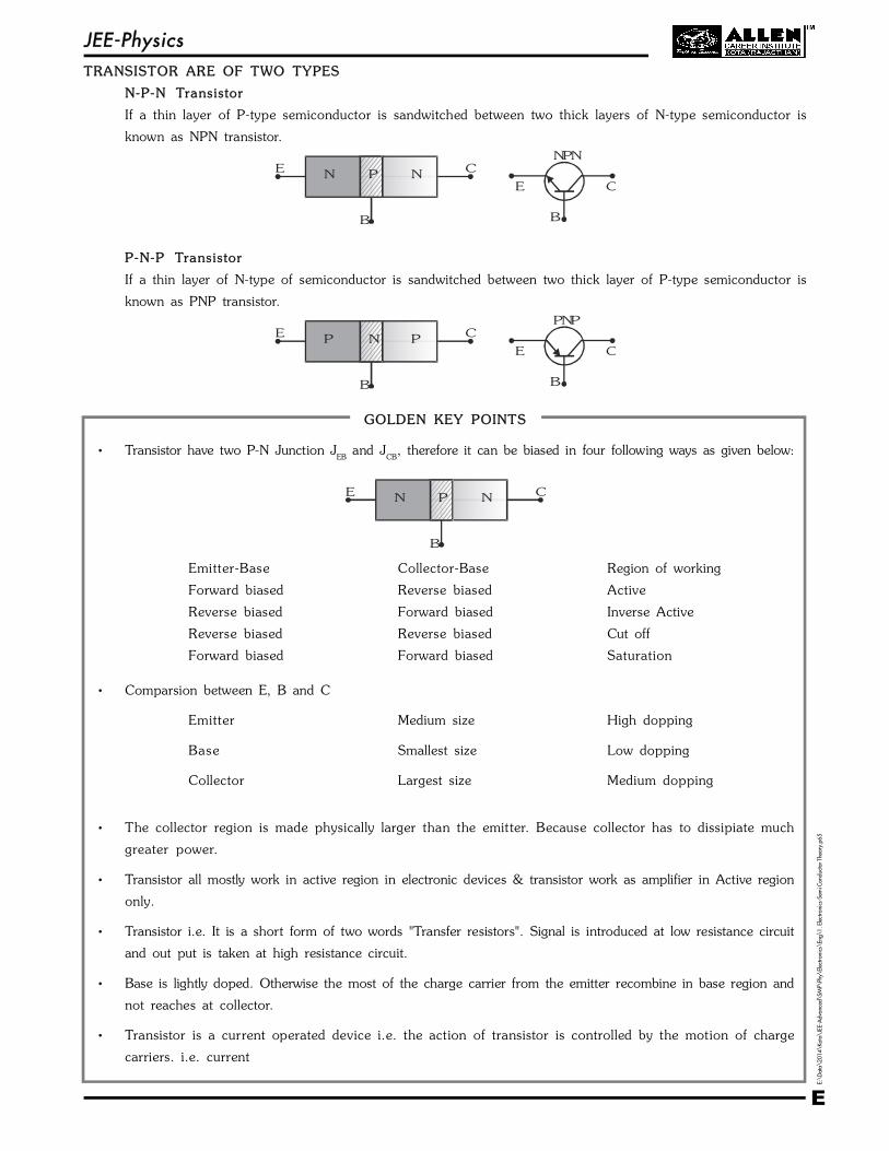
TRANSISTOR ARE OF TWO TYPES
N-P-N Transistor
If a thin layer of P-type semiconductor is sandwitched between two thick layers of N-type semiconductor is
known as NPN transistor.
E C
B
N NP
NPN
E C
B
P-N-P Transistor
If a thin layer of N-type of semiconductor is sandwitched between two thick layer of P-type semiconductor is
known as PNP transistor.
E C
B
P PN
PNP
E C
B
GOLDEN KEY POINTS
• Transistor have two P-N Junction JEB
and JCB
, therefore it can be biased in four following ways as given below:
E C
B
N NP
Emitter-Base Collector-Base Region of working
Forward biased Reverse biased Active
Reverse biased Forward biased Inverse Active
Reverse biased Reverse biased Cut off
Forward biased Forward biased Saturation
• Comparsion between E, B and C
Emitter Medium size High dopping
Base Smallest size Low dopping
Collector Largest size Medium dopping
• The collector region is made physically larger than the emitter. Because collector has to dissipiate much
greater power.
• Transistor all mostly work in active region in electronic devices & transistor work as amplifier in Active region
only.
• Transistor i.e. It is a short form of two words "Transfer resistors". Signal is introduced at low resistance circuit
and out put is taken at high resistance circuit.
• Base is lightly doped. Otherwise the most of the charge carrier from the emitter recombine in base region and
not reaches at collector.
• Transistor is a current operated device i.e. the action of transistor is controlled by the motion of charge
carriers. i.e. current
Page 21
JEE-Physics
E:\
Data
\2014\Kota
\JE
E-A
dva
nced
\SM
P\Ph
y\El
ectr
onic
s\Eng
\1. El
ectr
oni
cs-S
emi C
ond
uct
or Th
eory
.p65
E 21
WORKING OF NPN TRANSISTOR
The emitter Base junction is forward bias and collector base junction is reversed biased of n-p-n transistor in
circuit (A) and symbolic representation is shown in Figure.
h
mA E B C mA
IE IC
VCCIBVEE
IBVEEVCC
IE
N
IC
P N
emitter-basejunction
collectoremitter-basejunction
e
When emitter base junction is forward bias, electrons (majority carriers) in emitter are repelled toward base.
The barrier of emitter base junction is reduced and the electron enter the base, about 5% of these electron
recombine with hole in base region result in small current (Ib).
The remaining electron ( 95%) enter the collector region because they are attracted towards the positive
terminal of battery.
For each electron entering the positive terminal of the battery is connected with collector base junction an
electron from negative terminal of the battery connected with emitter base junction enters the region.
The emitter current (Ie) is more than the collector (I
c).
The base current is the difference between Ie and I
c and proportional to the number of electron hole recombination
in the base.
Ie = I
b +I
c
WORKING OF PNP TRANSISTOR
When emitter-base junction is forward biased holes (majority carriers) in the emitter are repelled towards the
base and diffuse through the emitter base junction. The barrier potential of emitter-base junction decreases and
hole enter the n-region (i.e. base). A small number of holes ( 5%) combine with electron of base-region resulting
small current (Ib). The remaining hole ( 95%) enter into the collector region because they are attracted towards
negative terminal of the battery connected with the collector-base junction. These hole constitute the collector
current (Ic).
N P
IE
mA
VEE
E B C
VCCIB
mA
ICIC
VCC
+IBVEE
P
emitter-basejunction
collectoremitter-basejunction
As one hole reaches the collector, it is neutralized by the battery. As soon as one electron and a hole is
neutralized in collector a covalent bond is broken in emitter region. The electron hole pair is produced. The
released electron enter the positive terminal of bettary and hole more towards the collector.
Page 22
JEE-Physics
E:\
Data
\2014\Kota
\JE
E-A
dva
nced
\SM
P\Ph
y\El
ectr
onic
s\Eng
\1. El
ectr
oni
cs-S
emi C
ond
uct
or Th
eory
.p65
22 E
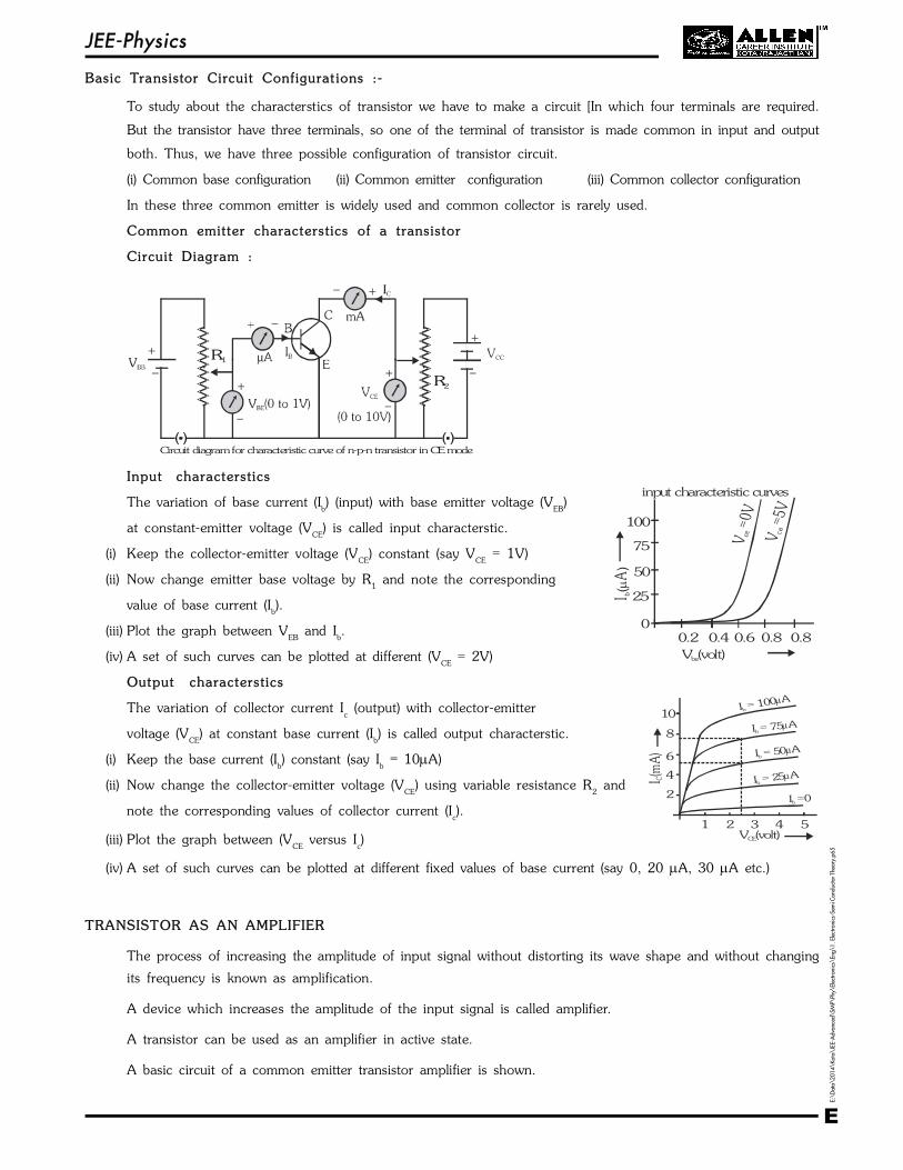
Basic Transistor Circui t Configurat ions :-
To study about the characterstics of transistor we have to make a circuit [In which four terminals are required.
But the transistor have three terminals, so one of the terminal of transistor is made common in input and output
both. Thus, we have three possible configuration of transistor circuit.
(i) Common base configuration (ii) Common emitter configuration (iii) Common collector configuration
In these three common emitter is widely used and common collector is rarely used.
Common emitter characterstics of a transistor
Circui t Diagram :
R1
Circuit diagram for characteristic curve of n-p-n transistor in CE mode( ) ( )
R2
Input characterstics
The variation of base current (Ib) (input) with base emitter voltage (V
EB)
at constant-emitter voltage (VCE
) is called input characterstic.
0.2 0.4
25
50
75
100
0
V (volt)be
0.6 0.8 0.8
V=0
Vce V
=5V
ce
I b(A
)
input characteristic curves
(i) Keep the collector-emitter voltage (VCE
) constant (say VCE
= 1V)
(ii) Now change emitter base voltage by R1 and note the corresponding
value of base current (Ib).
(iii) Plot the graph between VEB
and Ib.
(iv) A set of such curves can be plotted at different (VCE
= 2V)
Output characterstics
The variation of collector current Ic (output) with collector-emitter
voltage (VCE
) at constant base current (Ib) is called output characterstic.
(i) Keep the base current (Ib) constant (say I
b = 10A)
(ii) Now change the collector-emitter voltage (VCE
) using variable resistance R2 and
I = 75 Ab
I = 50 Ab
I = 100 Ab
1 2 3 54
I = 25 Ab
I(m
A)
C
VCE(volt)
I =0b2
4
6
8
10
note the corresponding values of collector current (Ic).
(iii) Plot the graph between (VCE
versus Ic)
(iv) A set of such curves can be plotted at different fixed values of base current (say 0, 20 A, 30 A etc.)
TRANSISTOR AS AN AMPLIFIER
The process of increasing the amplitude of input signal without distorting its wave shape and without changing
its frequency is known as amplification.
A device which increases the amplitude of the input signal is called amplifier.
A transistor can be used as an amplifier in active state.
A basic circuit of a common emitter transistor amplifier is shown.
Page 23
JEE-Physics
E:\
Data
\2014\Kota
\JE
E-A
dva
nced
\SM
P\Ph
y\El
ectr
onic
s\Eng
\1. El
ectr
oni
cs-S
emi C
ond
uct
or Th
eory
.p65
E 23
amplifiedoutput signal
BRL
VCC
VBB
IB
IC
+
ICIB
–
intput signal
–
Vi
VoE
C
+
+
–
IE
amplifier
common emitter amplifierNPN transistor
VCE
Comparative study of transistor configurations
1. Common Base (CB ) 2. Common Emitter (CE) 3. Common Collector (CC)
C B C E C C
CBE C
BB
IE
B BIB
IC
CEB C
EE
E
CIC
EIE
IBB
CCB E
CC
C
E
ICC
IEIB
B
Input Resistance Low (100 ) High (750 ) Very High 750 k
Output resistance Very High High Low
Current Gain (AI or ) (A
I or ) (A
I or )
= C
E
I
I = C
B
I
I = E
B
I
I
Voltage Gaino
V
i
VA
V =
C L
E i
I R
I R o
V
i
VA
V =
C L
B i
I R
I Ro
V
i
VA
V =
E L
B i
I R
I R
Lv
i
RA =
R L
v
i
RA =
R L
v
i
RA =
R
less than 1
Power Gaino
p
i
PA
P o
p
i
PA
P o
p
i
PA
P
2 Lp
i
RA
R
2 Lp
i
RA
R 2 L
p
i
RA
R
Phase di f ference same phase opposite phase same phase
(between output
and input)
App l i c a t ion For High Fequency For Audible fequency For Impedance Matching
Page 24
JEE-Physics
E:\
Data
\2014\Kota
\JE
E-A
dva
nced
\SM
P\Ph
y\El
ectr
onic
s\Eng
\1. El
ectr
oni
cs-S
emi C
ond
uct
or Th
eory
.p65
24 E
Relation Between and
IE = I
B + I
CIE = I
B + I
C --
divide by IC
divide by IB
1+
1-
E B
C C
I I1
I I CE
B B
II1+
I I 1
1-
1 1+ 1
1-
GOLDEN KEY POINTS
• In transistor charge carriers move from emitter to collector. Emitter send the charge carriers and collector
collect them this happen only when emitter-base junction is forward bias and collector-base junction is reverse
bias (base of amplifier)
• In transistor reverse bias is high as compared to forward bias so that the charge carriers move from emitter to
base exert a large attractive force to enter in collector region so base current is very less.
• CE configuration is widely used becasue it have large voltage and power gain as compared to other amplifiers.
• In amplifier negative feed back is used to stabilized the gain.
• CC is used for impdence matching for connecting two transistors in cascade.
Q .2 0 A transistor is a current operated device. Explain why ?
Ans . The action of a transistor is controlled by the charge carriers (electrons or holes). That is why a transistor is a
current operated device.
Q .2 1 In a transistor, reverse bias is quite high as compared to the forward bias. Why ?
Ans . In a transistor, charge carriers (electrons or holes) move from emitter to collector through the base. The reverse
bias on collector is made quite high so that it may exert a large attractive force on the charge carriers to enter
the collector region. These moving carriers in the collector constitute a collector current.
Q .2 2 A transistor is a temperature sensitive device. Explain.
Ans . In a transistor, conduction is due to the movement of current carriers electrons and holes. When temperature of
the transistor increases, many covalent bonds may break up, resulting in the formation of more electrons and
holes. Thus, the current will increase in the transistor. This current gives rise to the production of more heat
energy. the excess heat causes complete breakdown of the transistor.
Q .2 3 The use of a transistor in common-emitter configuration is preferred over the common-base configuration.
Explain why ?
Ans . The current gain and hence voltage gain in the common-emitter configuration is much more than i of common-
base configuration. Hence the former is preferred over the later.
Page 25
JEE-Physics
E:\
Data
\2014\Kota
\JE
E-A
dva
nced
\SM
P\Ph
y\El
ectr
onic
s\Eng
\1. El
ectr
oni
cs-S
emi C
ond
uct
or Th
eory
.p65
E 25
Q .2 4 Why do we prefer transistor over the vacuum tubes in the portable radio receivers ?
Ans . This is because of two reasons :
(i) Transistor is compact and small in size than the vacuum tube.
(ii) Transistor can operate even at low voltage which can be supplied with two or three dry cells.
Q .2 5 Why a transistor cannot be used as a rectifier ?
Ans . If transistor is to be used as a rectifier the either emitter-base or base-collector has to used as diode. For equated
working of the said set of diodes, the number density of charge carriers in emitter and base or base and collector
must be approximately same. As base is lightly doped and comparatively thin, so emitter cannot work as a
rectifier.
Ex.26 In a transistor, the value of is 50. Calculate the value of .
So l . = 501
50 =
1
50 – 50 =
50
51 = 0.98
Ex.27 Calculate the collector and emitter current for which Ib= 20 A, = 100
So l . = 100, Ib = 20 A
Ic = I
b = 100 × 20 × 10–6 = 2000 A
Ie = I
b + I
c = 20 + 2000 = 2020 A = 2.02 × 10⁻³ A = 2.02 mA
Ex.28 For a common emitter amplifier, current gain = 50. If the emitter current is 6.6 mA, calculate the collector and
base current. Also calculate current gain, When emitter is working as common base amplifier.
So l . = 50 ; Ie = 6.6 mA
c
b
I
I I
c = I
b = 50I
b...(i)
Ie = I
c + I
busing equation (i) we get 6.6 = 50 I
b + I
b = 51I
b
or b
6.6I
51 = 0.129 mA
HenceIc = 50 ×
6.6
51 = 6.47 mA and
1
=
500.98
51
Ex.29 Transistor with = 75 is connected to common-base configuration. What will be the maximu collector current
for an emitter current of 5 mA ?
So l . = 75, Ie = 5 mA
1
75 =
1
75 – 75 =
or 76 = 75 or =75
76
c
e
I
I I
c = I
e =
75
76 × 5 = 4.93 mA
Page 26
JEE-Physics
E:\
Data
\2014\Kota
\JE
E-A
dva
nced
\SM
P\Ph
y\El
ectr
onic
s\Eng
\1. El
ectr
oni
cs-S
emi C
ond
uct
or Th
eory
.p65
26 E
Ex.30 The base current is 100 A and collector current is 3 mA.
(a) Calculate the values of , Ie and
(b) A change of 20 A in the base current produces a change of 0.5 mA in the collector current. Calculate
a.c.
.
So l . Ib = 100 A = 0.100 mA, I
c = 3 mA
(a)c
b
I
I =
3
0.100 = 30
30 30
1 1 30 31
= 0.97 and I
e =
cI 3 31
30
= 3.1 mA
(b) Ib = 20 A = 0.02 mA , I
c = 0.5 mA
c
ac
b
I 0.5 25
I 0.02
Ex.31 In npn transistor circuit, the collector current is 10 mA. If 95% of the electrons emitted reach the collector, what
is the base current ?
So l . Ic = 95% I
c = 0.95 I
e
Ie = c
100 100I 10mA
95 95 = 10.53 mA ( I
c = 10 mA)
Now Ie = I
c + I
b I
b = I
e – I
c = 10.53 – 10 = 0.53 mA
Ex.32 In an NPN transistor 1010 electrons enter the emitter in 10–6 s and 2% electrons recombine with holes in base,
then current gain and are :
So l . Emitter current Ie
= Ne
t=
10 19
6
10 1.6 10
10
= 1.6 mA
Base current Ib =
21.6
100 = 0.032 mA
but Ie = I
c + I
b I
c = I
e – I
b = 1.6 – 0.032 = 1.568 mA
c
e
I 1.568 0.98
I 1.6
andc
b
I 1.56849
I 0.032
FE EDBA CK
Feedback are two types :
Posi t ive feedback
When input and output are in the same phase then positive feedback is there. It is used in oscillators.
Negative feedback
If input and output are out of phase and some part of that is feedback to input is known as negative feedback.
It is used to get constant gain amplifier.
Page 27
JEE-Physics
E:\
Data
\2014\Kota
\JE
E-A
dva
nced
\SM
P\Ph
y\El
ectr
onic
s\Eng
\1. El
ectr
oni
cs-S
emi C
ond
uct
or Th
eory
.p65
E 27
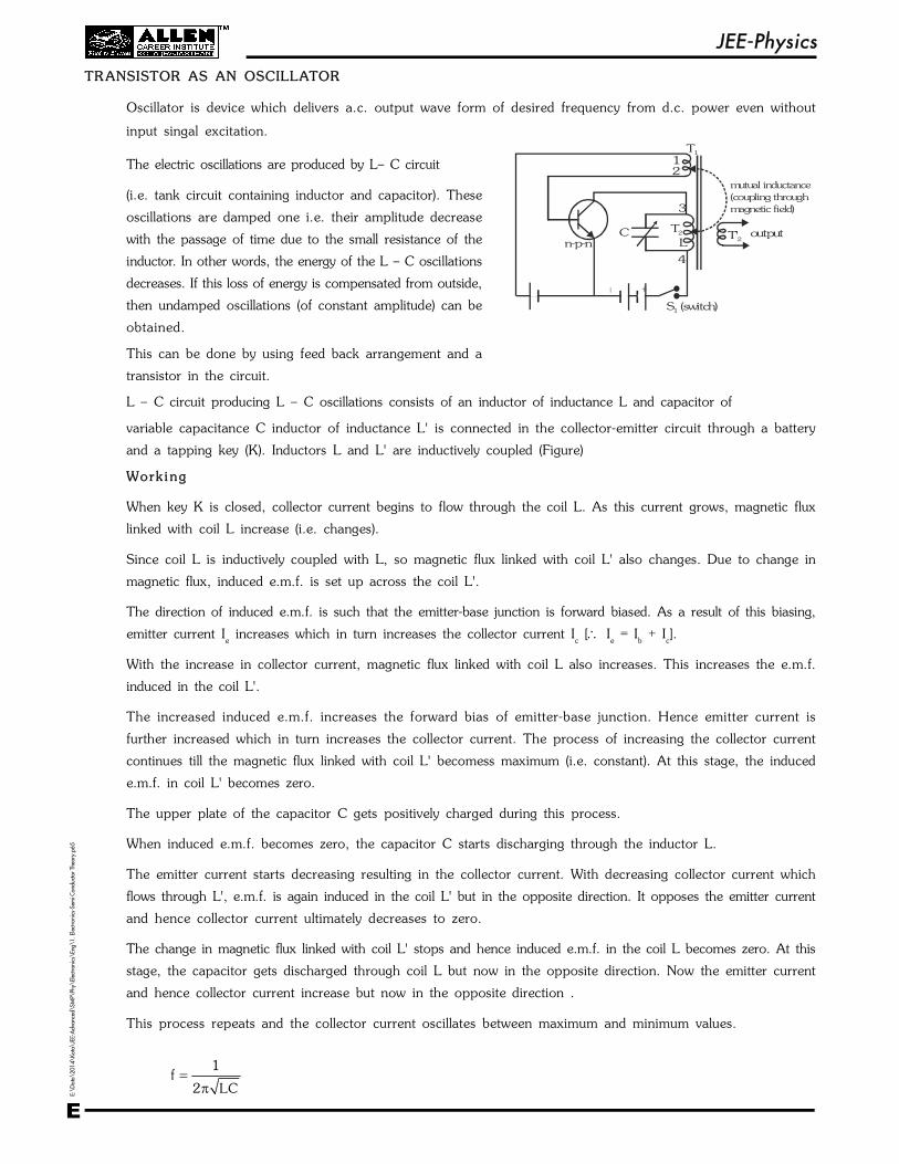
TR ANSISTOR AS AN OSCILLATOR
Oscillator is device which delivers a.c. output wave form of desired frequency from d.c. power even without
input singal excitation.
The electric oscillations are produced by L– C circuit
mutual inductance(coupling through magnetic field)
12
T1
T2' output
S1 (switch)
T2
3
L
4
n-p-nC
(i.e. tank circuit containing inductor and capacitor). These
oscillations are damped one i.e. their amplitude decrease
with the passage of time due to the small resistance of the
inductor. In other words, the energy of the L – C oscillations
decreases. If this loss of energy is compensated from outside,
then undamped oscillations (of constant amplitude) can be
obtained.
This can be done by using feed back arrangement and a
transistor in the circuit.
L – C circuit producing L – C oscillations consists of an inductor of inductance L and capacitor of
variable capacitance C inductor of inductance L' is connected in the collector-emitter circuit through a battery
and a tapping key (K). Inductors L and L' are inductively coupled (Figure)
Work i ng
When key K is closed, collector current begins to flow through the coil L. As this current grows, magnetic flux
linked with coil L increase (i.e. changes).
Since coil L is inductively coupled with L, so magnetic flux linked with coil L' also changes. Due to change in
magnetic flux, induced e.m.f. is set up across the coil L'.
The direction of induced e.m.f. is such that the emitter-base junction is forward biased. As a result of this biasing,
emitter current Ie increases which in turn increases the collector current I
c [ I
e = I
b + I
c].
With the increase in collector current, magnetic flux linked with coil L also increases. This increases the e.m.f.
induced in the coil L'.
The increased induced e.m.f. increases the forward bias of emitter-base junction. Hence emitter current is
further increased which in turn increases the collector current. The process of increasing the collector current
continues till the magnetic flux linked with coil L' becomess maximum (i.e. constant). At this stage, the induced
e.m.f. in coil L' becomes zero.
The upper plate of the capacitor C gets positively charged during this process.
When induced e.m.f. becomes zero, the capacitor C starts discharging through the inductor L.
The emitter current starts decreasing resulting in the collector current. With decreasing collector current which
flows through L', e.m.f. is again induced in the coil L' but in the opposite direction. It opposes the emitter current
and hence collector current ultimately decreases to zero.
The change in magnetic flux linked with coil L' stops and hence induced e.m.f. in the coil L becomes zero. At this
stage, the capacitor gets discharged through coil L but now in the opposite direction. Now the emitter current
and hence collector current increase but now in the opposite direction .
This process repeats and the collector current oscillates between maximum and minimum values.
1f
2 LC
Page 28
JEE-Physics
E:\
Data
\2014\Kota
\JE
E-A
dva
nced
\SM
P\Ph
y\El
ectr
onic
s\Eng
\1. El
ectr
oni
cs-S
emi C
ond
uct
or Th
eory
.p65
28 E
ADVANTAGES OF SEMICONDUCTOR DEVICES OVER VACUUM TUBES
Advan t a g e s
Semiconductor devices are very small in size as compared to the vacuum tubes. Hence the circuits using
semiconductor devices are more compact.
In vacuum tubes, current flows when the filament is heated and starts emitting electrons. So, we have to wait for
some time for the operation of the circuit. On the other hand, in semiconductor devices no heating is required
and the circuit begins to operate as soon as it switched on.
Semiconductor devices require low voltage for their operation as compared to the vacuum tube. So a lot of
electrical power is saved.
Semiconductor devices do not produce any humming noise which is large in case of vacuum tube.
Semiconductor devices have longer life than the vacuum tube. Vacuum tube gets damaged when its filament is
burnt.
Semiconductor devices are shock proof.
The cost of production of semiconductor-devices is very small as compared to the vacuum tubes.
Semiconductor devices can be easily transported as compared to vacuum tube.
D i s a d v an t a g e s
Semiconductor devices are heat sensitive. They get damaged due to overheating and high voltages. So they
have to be housed in a controlled temperature room.
The noise level in semiconductor devices is very high.
Semiconductor devices have poor response in high frequency range.
Q .3 3 Why is a transistor so called ?
Ans . The word Transistor can be treated as short form of two words 'transfer resistor'. In a transistor, a signal is
introduced in the low resistance circuit and output is taken across the high resistance circuit. Thus, a transistor
helps to transfer the current from low resistance part to the high resistance part.
Q .3 4 The base region of a transistor is lightly doped. Explain why ?
Ans . In a transistor, the majority carriers (holes or electrons) from emtter region move towards the collector region
through base. If base is made thick and highly doped, then majority of carriers from emitter will combine with
the carriers in the base and only small number of carriers will reach the collector. Thus the output or collector
current will be considerably small. To get large output or collector current, base is made thin and lightly doped
so that only few electron-hole combination may take place in the base region.
Q .3 5 Explain why the emitter is forward biased and the collector is reverse biased in a transistor ?
Ans . In a transistor, the charge carriers move from emitter to collector. The emitter sends the charge carriers and
collector collects them. This can happen only if emitter is forward biased and the collector is reverse biased so
that it may attract the carriers.