JEITA Technical Report of Japan Electronics and Information Technology Industries Association EIAJ EDR-7331 Design guideline of Integrated circuits for Quad Tape Carrier packages and Carrier ( QTP and Carrier ) Published in September, 2002 Investigated by Technical Standardization Committee on Semiconductor Device Package Published by Japan Electronics and Information Technology Industries Association
Transcript
JEITA
Technical Report of Japan Electronics and Information Technology Industries Association
EIAJ EDR-7331
Design guideline of Integrated circuits for Quad Tape Carrier packages and Carrier
( QTP and Carrier )
Published in September, 2002
Investigated by
Technical Standardization Committee on Semiconductor Device Package
Published by
Japan Electronics and Information Technology Industries Association
This document is a translation without guarantee. In the event of any doubt arising, the original standard in Japanese is to be evidenced. JEITA standards are established independently to any existing patents on the products, materials or processes they cover. JEITA assumes absolutely no responsibility toward parties applying these standards or toward patent owners. C 2002 by the Japan Electronics and Information Technology Industries Association All rights reserved. No part of this standard may be reproduced in any form or by any means without prior permission in writing from the publisher.
EIAJ EDR-7331
(1)
CONTENTS
Chapter 1 Design guideline of Integrated Circuits for Quad Tape Carrier Packages (QTP)
1. Scope of Application …………………………………………………………………………………………... 1
2. Definition of the Technical Terms …………………………………………………………………………….. 1
1. Objective of establishment …………………………………………………….………………………….... 30
2. History of review …………………………………………………….…………………………….…………... 30
3. Basic idea …………………………………………………….……………………………..……..…………... 32
4. QTP Background for dimensional provisions ……………….………………....…………………………... 33
5. QTP Carrier Background for dimensional provisions …………………….……………………………….. 40
6. The reference standard …………………………………….……………………………………………….. 42
7. Committee members ………………………….………………………………………………..…………… 43
EIAJ EDR-7331
- 1 -
Technical report of Japan Electronics and Information Technology Industries Association
Design guideline of Integrated circuits for Quad Tape Carrier packages and Carrier
( QTP and Carrier )
Chapter 1 1. Scope of Application
This technical report regulated outline drawings and dimensions about Quad Tape Carrier package
(hereinafter referred to as QTP), which is classified as form G among the Tape Carrier package
(hereinafter referred to as TCP) in EIAJ ED-7300 [Recommended practice on Standard for the preparation
of outline drawings of semiconductor packages].
Note: This technical report, chapter 1 are the revision version of EIAJ ED-7431A (General rules for the
preparation of outline drawings of integrated circuits, Quad Tape Carrier package), which the
establishment in April 1993. It did JEDEC JC-11 in the U.S.A and an opinion exchange and this
technical report was made. The related standards are shown below.
JEDEC standard UO- 018B (QTP, establishment in July 1993)
JEDEC standard US- 001B (QTP, establishment in November 1993)
JEDEC standard CS-006A (QTP Carrier, establishment in November 1993)
2. Definition of the Technical Terms
The definition of the technical terms used in this technical report is in conformity with EIAJ ED-7300, and
as for the new term, it depends on the following.
(1) Sprocket hole
The holes arrayed at the both sides of a tape at the constant pitch which are used feed the tape. 2
kinds of Super and Wide are prescribed by the size of the sprocket hole.
(2) Outerlead
The composition of the package, which was arranged because of the electric, mechanical and thermal
connection. It is defined as the terminal in EIAJ ED-7300.
(3) Test pad
The terminal part which was arranged outside outerlead to examine electricity.
(4) Lead pattern
The part which connects the interval of the IC and outerlead at the center and the interval of outerlead
and the test pad electrically in the wiring.
(5) Outerlead hole
The hole which was opened outside the package main unit to form outerlead.
(6) Corner tie bar
The part which separates outerlead hole in the part of the insulation tape which was prepared for the 4
corners of the main unit to maintain a package main unit in the insulation tape.
EIAJ EDR-7331
- 2 -
(7) Tooling hole
The hole which was opened by the insulation tape which was arranged in the corner of 4 of the
outside of the package main unit to use for the positioning of an electricity examination.
(8) Metal tooling hole
It forms a hole with the metallic foil in the purpose to improve positioning precision on the tooling hole.
It makes an option. (Explanatory note reference)
(9) Keeper bar
The figure of band's insulation tape, which is left at the outer lead tip to maintain the interval of the
outer lead in the package main unit by the later processing when separating from the insulation tape.
(10) Mouse ear
The part to have made extend a part on the outer lead hall to make it easy to form a keeper bar. It
makes an option. (Explanatory note reference)
(11) Tape format
The tape format 3 kinds are prescribed which 35 mm, 48 mm, 70 mm. The tape that forms a package
main unit inside the sprocket hole and by it the tape unit ranges with more than one piece of
continuation. DTP uses only 35 mm of tape format.
(12) Tape unit
The part of the tape, which was detached to contain one package main unit, the outerlead and the test
pad that is connected with it.
3. Background
Recent years, by the appearance of the electronic equipment with very thin types and multifunction, also
the integrated circuit package becomes numerous pin and becomes thin. It responds to the demand. This
technical report has a purpose of corresponding to use's increasing and promoting the standardization of
the package size and securing those compatibilities about Quad Tape Carrier package (hereinafter
referred to as QTP). This technical report intended to standardize the outer dimensions of QTP, which use
frequency rose, and ensure compatibility between products as far as possible for standardization.
4. Definition of QTP
The lead pattern forms in the insulation tape surface, which has a sprocket hole. And the package with the
4-direction lead, it comes out to the direction that is parallel to the seating plane outside the package body.
5. Numbering of Terminals
Basicaly, it follows the rule of EIAJ ED-7300. But it makes a package surface the surface where a lead
pattern is formed and it gives a number which is peculiar to each of the terminals and the test pads.
6. Nominal Dimensions
Package body size [symbol: D X E] is applied to Nominal dimension.
EIAJ EDR-7331
- 3 -
7. REFERENCE CHARACTERS AND DRAWING
7.1 QTP Outline Drawing (1)
Figure 1. (From surface of Cu pattern)
D3/E3A
C1
( )7 C
D1
B-C
B-C
C2
( )1
( )2 w2
v2
L A
M A
DS
S D
S
S
D
(DATUM -D-)
E2
D2B2
A
A1
( )7
B 7( )
S
S
E
( )E1
1 v1
( )2 w1
B-CAM
B1
S D
B-CAL S D
(DA
TUM
B-C
)D D
1
EIAJ EDR-7331
- 4 -
7.2 QTP Outline Drawing (2)
Figure 2 (From surface of Cu pattern)
( )5 e3
E2
e5
e4
( )
( )
4
5
E1
E
( )6
D1D
( )
( )
e35 5
e4(
)4e5 H D
2
EIAJ EDR-7331
- 5 -
7.3 QTP Test pad penumbra and outerlead penumbra detailed figure
Figure 3 (From surface of Cu pattern)
q
D
e( )
B-C
S
e1e2
( )5
( )5
b1 ( )8 b2
F1
AAz1
M
z2M
( )
( )
B-C
SS
D
B-C
SS
D
1 1
F2 B1
B2
J4
J3 3
y2 B-CAL S
y1 L A
( )
t2
t1
( )1
J1
bMX A E-F S
J2
S
S D
P
( )2
S
( )2
( )1
G S
B-C
1
M A S D S
B-CM A S D S
Note. (1) The maximum material requierments (Refer to ISO 2692/ JIS B 0023) apply to the positional tolerance of
outerleads and so on. (2) The least material requirements(Refer to ANSI Y14.5M)apply to the positional tolerance of test pads and
outside of outerlead hole. (3) Specifies the true geometric position of outerlead axis. (4) Specifies the true geometric position of tooling hole axis. (5) Specifies the true geometric position of test pad axis. (6) The Index mark makes the position of the corner part where the outerlead 1 pin exists. The Index mark
area, which is basically 1/16 with package body size, however in case of small package body size, it is less than 1/4 with package body size, It must be included in the shaded area entirely.
(7) Datum plane is supposed to be found from center distance sprocket hole of datum B C D . However, datum plane of outerlead supposes that it finds from the test pad of datum E F G .
(8) 凸 part (Indicated by b1 x b2) with outerlead number 1 shows an index mark. (9) The measurement in datum plane, it in the condition which lost a curve. It is scissors in the tape by the
glass board and so on. (10) It makes the round quantity of pulling-out hole corner of the tape equal to or less than 0.20 mm.
EIAJ EDR-7331
- 6 -
8. QTP outer dimension Table 1 below shows the standard dimensions. Combinations of the standard dimensions shown below allow a number of package variations. If a package is newly designed, their dimensions shall be selected in the Table 10. Standard Package List.
Table 1
Unit: mm
Description Reference
symbol Standards Recommended Remarks
Nominal dimension
D x E
(1) Package body size [symbol: D x E] is applied to Nominal dimension. (2) Nominal dimension is shown below.
D x E 14.00 x 14.00 16.00 x 16.00 18.00 x 18.00 20.00 x 20.00 24.00 x 24.00 26.00 x 26.00 28.00 x 28.00 32.00 x 32.00 36.00 x 36.00 40.00 x 40.00
_
(1) Nominal dimension is equal to package body size [symbol: D x E].
Package width
E
Package
length D
(1) It prescribes a standard value as in the following formula. E nom (D nom ) = 16.00 + 4k k = 0, 1, 2, 3,4,5,6 (2) It adds the following value to the standard value.
In case of tape format D2=35, E=16.00, 18.00 In case of tape format D2=48, E=26.00
(3) It makes a tolerance of package width, length as follows. E = E nom ±0.10 D = D nom ±0.10 (4) It makes package width, length as follows.
_
(1) It considered for package body size (D x E) which becomes Nominal dimension to get to do the same becoming of series with QFP.
(2) It prescribes a body size (DXE) according to the tape format(D2), respectively.
(3) It makes the same rule with JEDEC standard US- 001B.
D2 35 48 70
14.00 x 14.00 - -
16.00 x 16.00 16.00 x 16.00 -
18.00 x 18.00 - -
20.00 x 20.00 20.00 x 20.00 -
24.00 x 24.00 24.00 x 24.00 24.00 x 24.00
- 26.00 x 26.00 -
28.00 x 28.00 28.00 x 28.00 28.00 x 28.00
32.00 x 32.00 32.00 x 32.00 32.00 x 32.00
36.00 x 36.00 36.00 x 36.00 36.00 x 36.00
D x E
40.00 x 40.00 40.00 x 40.00 40.00 x 40.00
EIAJ EDR-7331
- 7 -
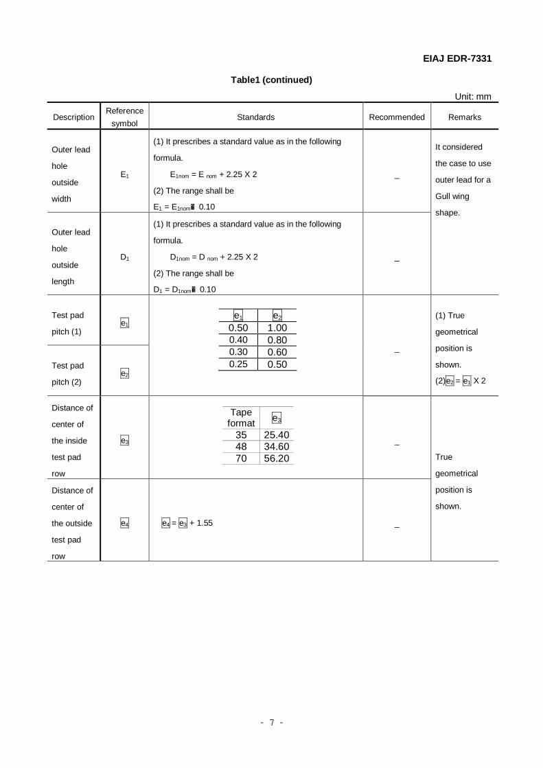
Table1 (continued)
Unit: mm
Description Reference
symbol Standards Recommended Remarks
Outer lead
hole
outside
width
E1
(1) It prescribes a standard value as in the following
formula.
E1nom = E nom + 2.25 X 2
(2) The range shall be
E1 = E1nom±0.10
_
Outer lead
hole
outside
length
D1
(1) It prescribes a standard value as in the following
formula.
D1nom = D nom + 2.25 X 2
(2) The range shall be
D1 = D1nom±0.10
_
It considered
the case to use
outer lead for a
Gull wing
shape.
Test pad
pitch (1) e1
Test pad
pitch (2) e2
_
(1) True
geometrical
position is
shown.
(2)e2 = e1 X 2
Distance of
center of
the inside
test pad
row
e3
_
Distance of
center of
the outside
test pad
row
e4 e4 = e3 + 1.55 _
True
geometrical
position is
shown.
Tape format e3
35 25.40 48 34.60 70 56.20
e1 e2 0.50 1.00 0.40 0.80 0.30 0.60 0.25 0.50
EIAJ EDR-7331
- 8 -
Table1 (continued)
Unit: mm
Description Reference
symbol Standards Recommended Remarks
Test pad width
B1
The range shall be B1 = B1nom±0.03
_
Test pad length
B2
(1) B2nom = 0.65
(2) The range shall be B2 = B2nom ±0.03
_
There is a shape of the center test pad like the following figure to make the standard of datum line.
Tolerance of test pad center position (1)
y1
(1) Tolerance of test pad center position shall be specified in the outline drawing. (2) Reference symbol “y1” shall be replaced as below. _ _
Tolerance of test pad center position (2)
y2
(1) Tolerance of test pad center position shall be specified in the outline drawing. (2) Reference symbol “y2” shall be replaced as below.
y2 ≦0.10
_ _
e B1nom
0.50 0.70 0.40 0.50 0.30 0.40 0.25 0.32
y1 Ⓛ
e y1 0.50 0.10 0.40 0.08 0.30 0.08 0.25 0.05
y2 Ⓛ
One side is an even number.
90°
B2
B1
90° B1
One side is an odd number.
EIAJ EDR-7331
- 9 -
Table1 (continued)
Unit: mm
Description Reference
symbol Standards
Recommended
Remarks
Test pad layout
_
(1) It prescribes a test pad layout as follows.
(2) It makes a test pad layout with 2 lines of plover layout and moreover it makes most outside an end test pad of the line outside. (3) The package center and the test pad center of line outside agree. (4) It doesn't use a test pad at the center as the principle.
_
It makes 4 test pads on the datum line a shape like the following figure as the mark.
90
EIAJ EDR-7331
- 10 -
Number of test pads
N
(1) It prescribes a test pad layout as follows.
_
(1) It is due to the rule of the test pad layout.
(2) It makes g1min=1.10mm which a minimum value during the test pad and the tolling hole center. It prescribes ”N” which number of maximum test pads and it is stored among tooling hole center distance (e5).
(3) The test pad provides the number of maximum test pads regardless of the number of outer leads.
Tape format 35 48 70 e =0.50 196 260 436 e =0.40 244 324 548 e =0.30 324 436 724 e =0.25 338 532 884
EIAJ EDR-7331
- 11 -
Table1 (continued)
Unit: mm
Description Reference
symbol Standards Recommended Remarks
Outer lead layout
_
(1) It prescribes outer lead layout as follows.
(2) The outer lead center shifts to the package center in e /2. (3) But, in the following case, the package center and outer lead center agree. Nominal dimension 20.00X20.00 of tape format 35 Nominal dimension 28.00X28.00 of tape format 48
_ _
Outer lead pitch
e
_
True geometrical position is shown.
Number of outer leads
n
(1) It prescribes the number of outer leads as follows.
(1-1) It is due to the rule of the outer leads layout. (1-2) It makes g2min=0.95mm, which a minimum value between outside of outer lead at the end most and package unit corner. It makes either smaller ones ”n” that maximum number of terminal or number of test pad (N). It’s enters package width (Enom) or package length (Dnom). (2) “n” value See 10. Standard Package List.
_
As for the way of calculating the number of outer leads, it refers to explanatory note.
e 0.50 0.40 0.30 0.25 0.20 0.15
EIAJ EDR-7331
- 12 -
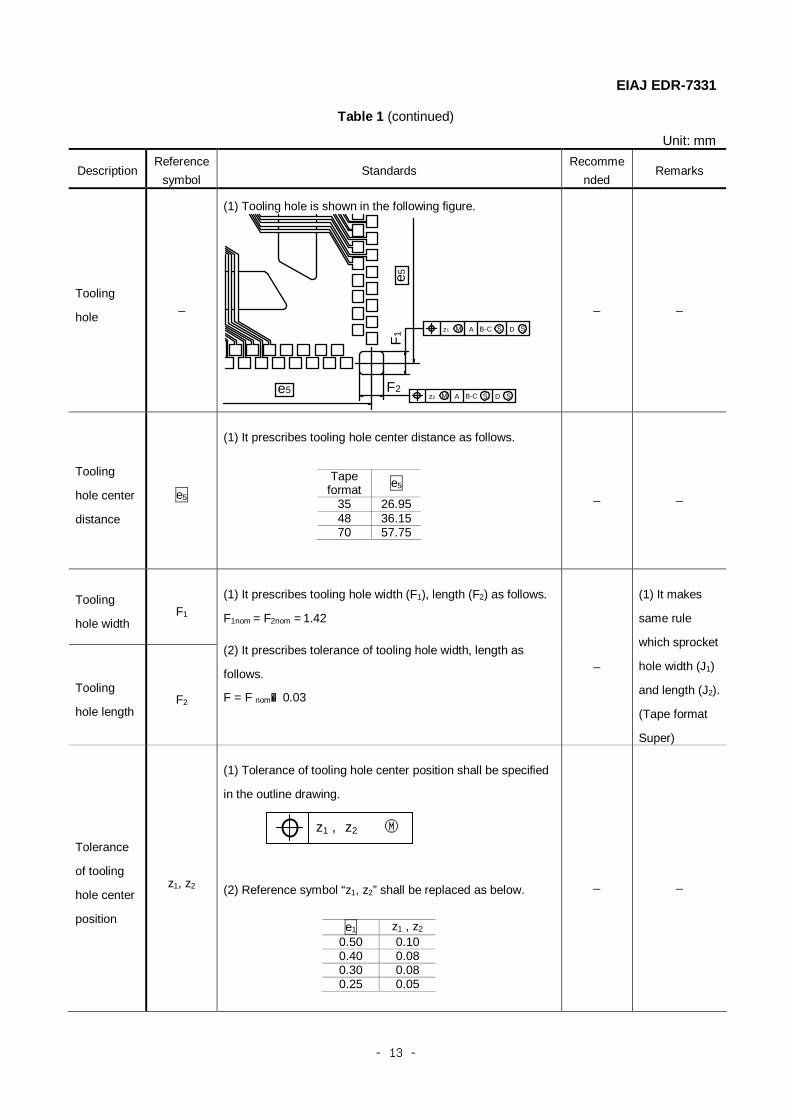
Table 1 (continued)
Unit: mm
Description Reference
symbol Standards
Recommend-ed
Remarks
Outer lead
width b
It makes a maximum and a minimum value a range in
the table below, to each outer lead pitch.
_ _
Tolerance
of outer
lead center
position
x
(1) Tolerance of outer lead center position shall be
S S nom = 1.00 _ It makes the same rule with DTP(2).
Corner tie bar angle
θ θnom = 60° _ _
Sprocket hole width
J1 , J3
Sprocket
hole
length
J2 , J4
(1) It prescribes a standard value below. (2) It prescribes tolerance of sprocket hole width, length as follows.
J = J nom±0.03
_
(1) kind of the sprocket hole are in following of 2 type of tape formats, Super and Wide. Super : J nom=1.42 Wide : J nom=1.98 (2) J1 and J2 are sprocket hole in the package center. J3 and J4 are the other sprocket hole.
Sprocket
hole pitch P
(1) P nom = 4.75
(2) The range shall be
P = P nom ± 0.05 _ _
Tape format J1nom=J3nom J2nom=J4nom
35 Super 1.42 Super 1.98 48 Wide 1.42 Super 1.98 70 Wide 1.42
EIAJ EDR-7331
- 15 -
Table 1 (continued)
Unit: mm
Description Reference
symbol Standards Recommended Remarks
Distance of
center of the
sprocket hole
row
H
(1) It prescribes as in the table below.
_
(1) Range of tape
format 35 shall be
H = Hnom +0.04-0.07
(2) Range of tape
format 48,70 shall
be
H = Hnom±0.08
Outer lead
hole width E1
(1) It prescribes a standard value as in the following
formula.
E1nom= Enom +(0.35 X 2)
(2) The range shall be
E1 = E1nom±0.15
_ _
Package
thickness A
Anom = 0.50
It makes the same
rule with JEDEC
standard US-
001B.
Package
upper part
thickness
A1
_
It makes the same
rule with JEDEC
standard US-
001B.
Sealing
length D3 D3≦D _
Sealing width E3 E3≦E _
It makes the same
rule with DTP(1),
DTP(2).
Tape format Hmin Hnom Hmax 35 Super 31.76 31.83 31.87
Super 42.10 42.18 42.26 48 Wide 44.78 44.86 44.94 Super 63.87 63.95 64.03 70 Wide 66.72 66.80 66.88
Tape format Amax
35 2.55 48 4.45 70 4.45
Tape format A1max
35 1.50 48 2.70 70 2.70
EIAJ EDR-7331
- 16 -
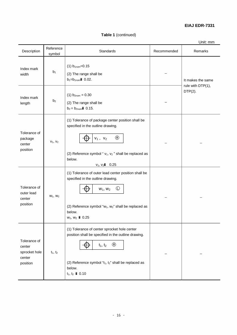
Table 1 (continued)
Unit: mm
Description Reference
symbol Standards Recommended Remarks
Index mark width
b1 (1) b1nom=0.15
(2) The range shall be b1=b1nom±0.02.
_
Index mark length
b2 (1) b2nom = 0.30
(2) The range shall be b2 = b2nom±0.15.
_
It makes the same rule with DTP(1), DTP(2).
Tolerance of package center position
v1, v2
(1) Tolerance of package center position shall be specified in the outline drawing. (2) Reference symbol “ v1, v2 ” shall be replaced as below. v1, v2≦ 0.25
_ _
Tolerance of outer lead center position
w1, w2
(1) Tolerance of outer lead center position shall be specified in the outline drawing. (2) Reference symbol “w1, w2” shall be replaced as below. w1, w2 ≦0.25
_ _
Tolerance of center sprocket hole center position
t1, t2
(1) Tolerance of center sprocket hole center position shall be specified in the outline drawing. (2) Reference symbol “t1, t2” shall be replaced as below. t1, t2 ≦0.10
_ _
t1, t2 Ⓜ
v1 , v2 Ⓜ
w1, w2 Ⓛ
EIAJ EDR-7331
- 17 -
9. Standard Registration
When you need to register a new outline specification on the standard, complete the appendix format 5 in
Technical Standardization Committee on Semiconductor Device Package steering rule, in compliance with
the Standardization Rule. In order to make a package dimension table, which come under Item 2,
Appendix format 5, fill the dimensions marked with ( レ ) in the following Table.
The rule item of the TCP (QTP, DTP(1), DTP (2)) standard exceeds 30 items. Therefore, complexly when
making individual standard registration completely. Then it made the registration table to have narrowed
down to the item, which the minimum outward form size needs.
Incidentally, it supposes that it enters package code form type according to EIAJ ED-7303B (Name and
Code for Integrated Circuits Package).
Table 2
Serial Number External Type T-QTP○○- ○○.○○X○○.○○-○.○○
Reference Symbol min nom max D2 レ
P レ
H レ
E レ
E1 レ レ レ
E2 レ レ レ
D レ
D1 レ レ レ
A レ
A1 レ
b レ レ
e レ(*) e1 レ(*) e2 レ(*) e3 レ(*) e4 レ(*) e5 レ(*) n レ N レ
J1, J3 レ J2, J4 レ
F1 レ
Group1
F2 レ
(*) true geometrical position
EIAJ EDR-7331
- 18 -
10. Standard Package List To further clarify the combinations of part dimensions, the combinations of recommended package classifications shall be indicated as shown below as assistance in the design and development of new package in the future.
10.1 Code that is “serial number” of the standard package list is shown in explanation table 1. (It makes the same rule with JEDEC standard US- 001B)
Explanation table 1 Tape
format Package body size Test pad pitch(1)
Outer lead pitch
D2 1st DXE 2nd e1 3rd e 4th 35S A 14.00X14.00 A 0.50 1 0.50 1 48S B 16.00X16.00 B 0.40 2 0.40 2 70S C 18.00X18.00 C 0.30 3 0.30 3 48W D 20.00X20.00 D 0.25 4 0.25 4 70W E 24.00X24.00 E 0.20 5 0.20 5
26.00X26.00 F 0.15 6 0.15 6 28.00X28.00 G 0.10 7 0.10 7 32.00X32.00 H 0.08 8 36.00X36.00 J 0.065 9
40.00X40.00 K 0.050 -
Table 2 Standard Package Dimension List (1/2)
Numerical value in the table (number of the terminals: n)
Test pad pitch(1)
Tape format
S: Super W: Wide
Test pad N
Package body size e=0.50 e=0.40 e=0.30 e=0.25 e=0.20 e=0.15
40.00X40.00 (XK-XX) 304 376 504 544(*1) 544(*1) -(*2) Note (*1) limitation on the number of the pins by the test pad
(*2) Between outer lead to test pad design rule(Line/Space=60μm/60μm) (*3) There is not an outer lead area, Between outer lead to test pad design rule. (*4) There is not an area, Between outer lead to test pad design rule.
(*5) The decrease of the number of the pins, because g2 range is too small.
EIAJ EDR-7331
- 19 -
Table 3 Standard Package Dimension List (2/2)
Numerical value in the table (number of the terminals: n)
Test pad
pitch(1)
Tape format
S: Super W: Wide
Test pad N
Package body size e=0.50 e=0.40 e=0.30 e=0.25 e=0.20 e=0.15
40.00X40.00 (XK-XX) 304 376 504 608 760 -(*2) Note (*1) limitation on the number of the pins by the test pad
(*2) Between outer lead to test pad design rule(Line/Space=60μm/60μm) (*3) There is not an outer lead area, Between outer lead to test pad design rule. (*4) There is not an area, Between outer lead to test pad design rule.
(*5) The decrease of the number of the pins, because g2 range is too small.
EIAJ EDR-7331
- 20 -
Chapter 2 1. Scope of Application
This technical report regulated outline drawings and dimensions about Quad Tape Carrier package Carrier (hereinafter referred to as QTP Carrier). QTP Carrier, which is used for QTP. And QTP is classified as form G among the Tape Carrier package (hereinafter referred to as TCP) in EIAJ ED-7300 [Recommended practice on Standard for the preparation of outline drawings of semiconductor packages].
Note: This technical report, chapter 2 are the revision version of EIAJ ED-7431-1A (Recommended outline drawings for Carriers, Quad Tape Carrier package Carriers), which the establishment in February 1994. It did JEDEC JC-11 in the U.S.A and an opinion exchange and this technical report was made. The related standards are shown below. JEDEC standard UO-018B (QTP, establishment in July 1993) JEDEC standard US-001B (QTP, establishment in November 1993) JEDEC standard CS-006A (QTP Carrier, establishment in November 1993)
2. Definition of the Technical Terms The definition of the technical terms used in this technical report is in conformity with EIAJ ED-7300, and as for the new term, it depends on the following.
2.1 QTP (1) Sprocket hole
The holes arrayed at the both sides of a tape at the constant pitch which are used feed the tape. 2 kinds of Super and Wide are prescribed by the size of the sprocket hole.
(2) Test pad The terminal part which was arranged outside outerlead to examine electricity.
(3) Tooling hole The hole which was opened by the insulation tape which was arranged in the corner of 4 of the outside of the package main unit to use for the positioning of an electricity examination.
(4) Tape format The tape format 3 kinds are prescribed which 35 mm, 48 mm, 70 mm. The tape that forms a package main unit inside the sprocket hole and by it the tape unit ranges with more than one piece of continuation. DTP uses only 35 mm of tape format.
(5) Tape unit The part of the tape, which was detached to contain one package main unit, the outerlead and the test pad that is connected with it.
2.2 QTP Carrier (1) Registration hole
The hole which was provided at the same position as the center hole of the QTP sprocket hole. (2) Tape retention area
The area provide a support for retaining the tape at the carrier. The support shall mean an elastic hook in case of one peace type and a cover to secure the tape in case of two-peace type.
(3) Tape fine alignment hole The hole which was provided for position which is same as the tooling hole of QTP. In case of the positioning with the socket and so on, the escape hole of alignment pin which is inserted in the tooling hole.
(4) Opening The escape hole which is located at the center of the carrier for the package lead to be cut.
EIAJ EDR-7331
- 21 -
3. Background
Recent years, by the appearance of the electronic equipment with very thin types and multifunction, also
the integrated circuit package becomes numerous pin and becomes thin. It responds to the demand. The
use of QTP increased. QTP considers handling by the process, it generally inserts in the carrier and an
electricity examination, processing(cutting of the lead and so on), conveyance and so on are done. This
technology report has a purpose of promoting the standardization of the QTP Carrier size and securing an
automatic machine, a storage magazine and the compatibility of the test socket. It aims for a design
standard value, i.e. a concept in the design center to be shown as much as possible about hitting a rule
with each size and to improve a role as the standardization index.
4. Definition of QTP Carrier
The case for the conveyance to protect QTP and to facilitate treatment.
5. The way of putting an index
In 4 corners of the QTP carrier, it C shape cuts only 1 corner. Basicaly, it makes the corner index which is
the same as 1st pin of the terminal and 1st of the test pad of QTP.
6. Nominal Dimensions
It combines and it calls a used tape format and the initial of Super and Wide.
EIAJ EDR-7331
- 22 -
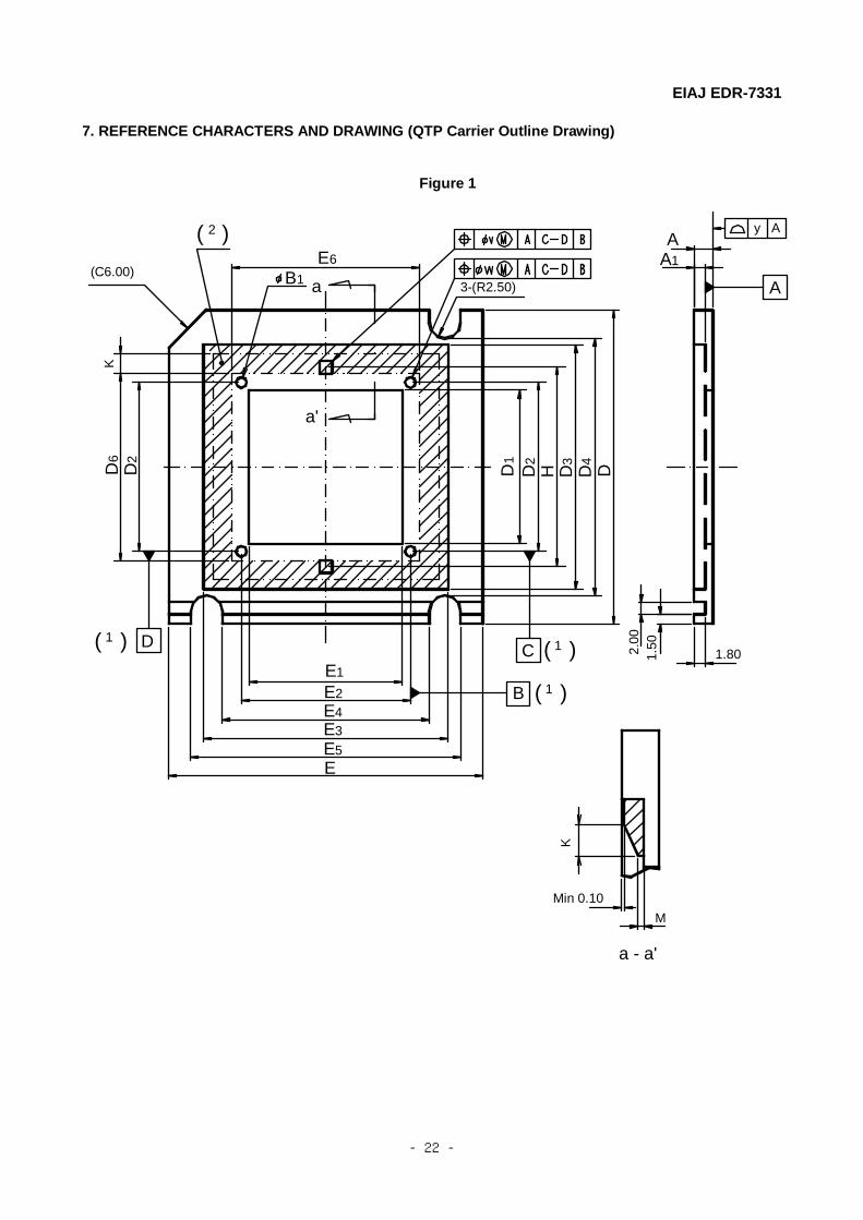
7. REFERENCE CHARACTERS AND DRAWING (QTP Carrier Outline Drawing)
Note(1) Datum plane finds from the tape fine alignment hole center interval that B C D . However, It supposes that the big type with the width (E1) and length (D1) of the opening finds datum E and F , because the tape fine alignment hole doesn't exist. (Figure 4 reference)
(2) The slanted line part shows tape retension area. (3) It considers permission by the cutting size of the tape. It prepared the QTP carrier, which can
correspond to the size with big cutting size as the option. It makes the width (E1) of the opening and the length (D1) of the opening as follows.
In case of 35 mm of tape formats, D1= E1=30.00mm In case of 48 mm of tape formats, D1= E1=40.00mm
EIAJ EDR-7331
- 24 -
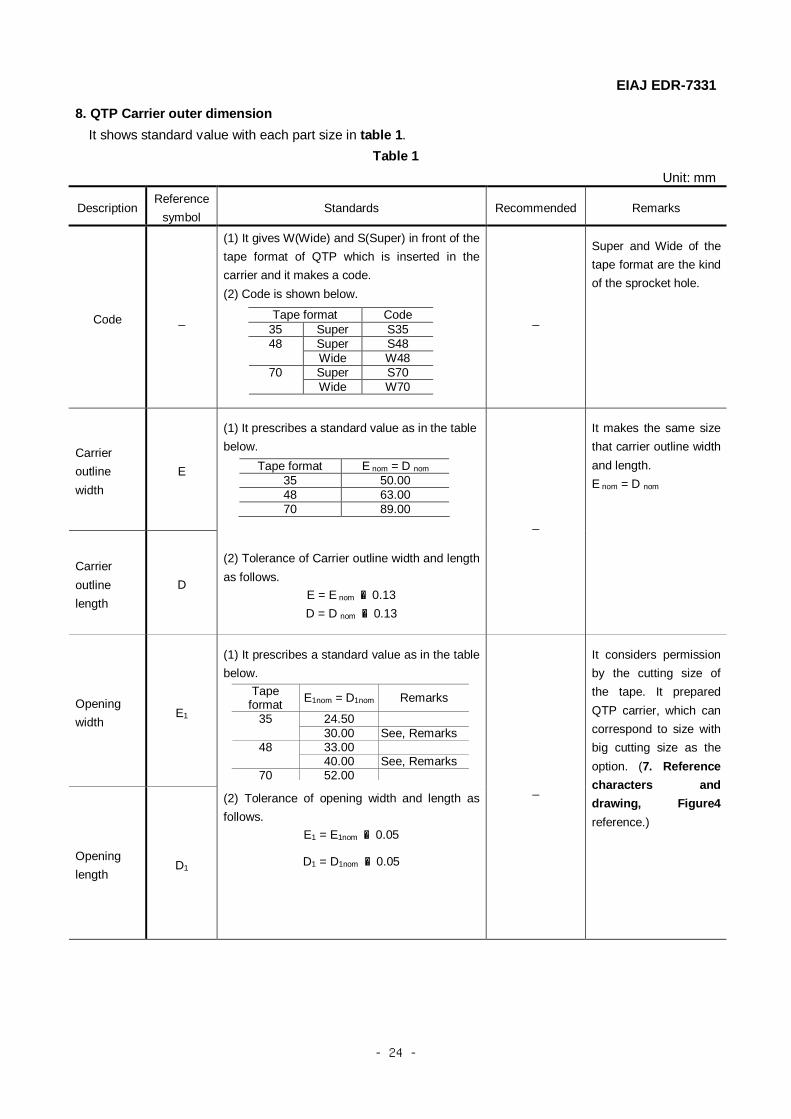
8. QTP Carrier outer dimension It shows standard value with each part size in table 1.
Table 1 Unit: mm
Description Reference
symbol Standards Recommended Remarks
Code _
(1) It gives W(Wide) and S(Super) in front of the tape format of QTP which is inserted in the carrier and it makes a code. (2) Code is shown below.
_
Super and Wide of the tape format are the kind of the sprocket hole.
Carrier outline width
E
Carrier outline length
D
(1) It prescribes a standard value as in the table below. (2) Tolerance of Carrier outline width and length as follows.
E = E nom ±0.13 D = D nom ±0.13
_
It makes the same size that carrier outline width and length. E nom = D nom
Opening width
E1
Opening length
D1
(1) It prescribes a standard value as in the table below.
(2) Tolerance of opening width and length as follows.
E1 = E1nom ±0.05
D1 = D1nom ±0.05
_
It considers permission by the cutting size of the tape. It prepared QTP carrier, which can correspond to size with big cutting size as the option. (7. Reference characters and drawing, Figure4 reference.)
Tape format Code 35 Super S35
Super S48 48 Wide W48 Super S70 70 Wide W70
Tape format E nom = D nom 35 50.00 48 63.00 70 89.00
Tape format E1nom = D1nom Remarks
24.50 35 30.00 See, Remarks 33.00 48 40.00 See, Remarks
70 52.00
EIAJ EDR-7331
- 25 -
Table 1 (continued) Unit: mm
Description Reference
symbol Standards
Recommended
Remarks
E2
Distance between the tape fine alignment hole
D2
(1) It prescribes a standard value as in the table below.
D
D2
B1
E2 B CD
2
_
It makes the value, which is the same as tooling hole center distance (e5).
Tolerance of tape fine alignment hole center position
w
(1) Tolerance of tape fine alignment hole center position shall be specified in the outline drawing. (2) Reference symbol “ w ” shall be replaced as below.
w ≦0.10
_ _
Diameter of tape fine alignment hole
φB1
It considers and it prescribes the permission value of Tooling hole width (F1) and length (F2) and tolerance of tooling hole center position of QTP as follows.
This technical report accounts for the industrial standard of Quad Tape Carrier packages and Carrier (hereinafter referred to as QTP, QTP Carrier). It was established to provide the design guideline of QTP and QTP Carrier when it is made in to product or when Automatic mounting machinery and associated parts are developed.
2. History of review
Recently, electronic appliances become smaller and their functions are diversified, and the terminals integrated circuits increase rapidly. On such background, demand to the thin and numerous pin package increase. As for QTP, effectively was admitted as the numerous pin package which is possible to with equal to or less than 0.50 mm of outer lead pitch of surface mount device. It expected that the application range expanded. It stores up to correspond to the trend, in April 1989, it starts " TCP standardization WG " which was under Special Technical Committee on Semiconductor Device Package Outlines (currently, Technical Standardization Committee on Semiconductor Device Package). It fixed as taking up standard creating by the standardization of DTP (1), DTP (2) and QTP as the business plan. First, to deliberate about DTP (1), DTP (2) after deciding a basic item about QTP was fixed. After that, in 1991, TCP standardization WG disperses. It wasn't deliberated for about 1 year because to have been taken over by the plastic package subcommittee (currently, Integrated Circuits Package Subcommittee) but the professional field was different. Recurrence addition " TCP standardization WG " and a full-scale deliberation were begun in April 1992. At abroad, as the standard of QTP, UO-017A (establishment in October, 1988) existed and it was standardized by JC-11 under Joint Electron Device Engineering Council (hereinafter referred to as JEDEC). However, there was a part which is difficult about both standardization concept and manufacturing technology. Therefore, it established QTP outline general rule newly. The deliberation became the long-range interval, because it crossed to varying as QTP and QTP Carrier that is used for the conveyance and testing, it discuss at the same time. The other hand, UO-018B (Metric TAB, establishment in July, 1993) that JEDEC improved UO-017A was deliberated and was being established. US-001B (establishment in November, 1993), too, was deliberated based on these and was being established. Also, The standard of the QTP Carrier, too, was deliberated as CS-006A (establishment in November, 1993) and was being established. A deliberation was carried forward while considering these standard plans in TCP standardization WG. In April 1993, QTCP which was former name was changed QTP at the Special Technical Committee on Semiconductor Device Package Outlines. Also A working group name, too, was changed with " Tape Carrier Package WG ". The standardization of the package naming was deliberated in " General rule package standardization WG " (currently, general rule of semiconductor package Subcommittee), which is under The Special Technical Committee on Semiconductor Device Package Outlines. This change is because the 4 character composition of QTCP which becomes basic type of the package form came off the standard. But, the name of QTP was approved in "Quad Tape Carrier package". Via above mentioned deliberation elapse, Tape Carrier package WG ends the last deliberation in 1993, and pass in the semiconductor package special committee approval. It was established as JEITA standard EIAJ ED-7431 (QTP) in April 1993 and EIAJ ED-7431-1 (QTP Carrier) in February 1994. After that, when showing EIAJ ED-7431 (QTP) and EIAJ ED-7431-1 (QTP Carrier) to JEDEC, JC11 in
EIAJ EDR-7331
- 31 -
May 1994 at JWG#2 Kobe conference, it pointed out the mistake match of JEDEC standards US- 001B (QTP) and CS-006A (QTP Carrier) from the JEDEC side. The point that, EIAJ ED-7431 and EIAJ ED-7431-1 doesn't fit the rule value(recommendation value) of US-001B and CS-006A. Then, JEDEC opinion which can not admit EIAJ ED-7431 and EIAJ ED-7431-1 was shown. Also, before this pointing-out, it consulted an opinion in the JEITA side, too, and there was a background to have deliberated JEDEC standard of QTP and the QTP carrier so far for about 5 years. Receiving this, in June1994, to revise for EIAJ ED-7431 and EIAJ ED-7431-1 to agree with US-001B and CS-006A were fixed at Tape Carrier Package WG. EIAJ ED-7431A (QTP) was revised in October 1994, and EIAJ ED-7431-1A (QTP Carrier) was revised in December 1994. In January, 2002, It began questionnaire investigation about the reconsideration of the elapse in 10 years about the TCP standards (QTP, DTP(1), DTP(2)) in Integrated Circuits Package Subcommittee. As a result, There is an answer from 12 companies in Japan, and the opinion that equal to or more than 2 companies, the revision (It keeps just as it is) are necessary was gotten about the TCP standards (QTP, DTP(1), DTP (2)). In March 2002, it was fixed that to carry forward the revision of the TCP standards in WG. Also, the consideration when implementing a standardization proposal by IEC, SC47D/WG1, According to the IEC format, we placed in the design guide of integrated circuits package as the classification. QTP relation technical report was established in September 2002 as EIAJ EDR-7331 (QTP and QTP Carrier).
TCP relation standard, the following standard exists and results in the today. (1) EIAJ ED-7431, EIAJ ED-7431A (General rules for the preparation of outline drawings of integrated
circuits, Quad Tape Carrier package (QTP)), The deliberation begins from April 1989 by " TCP standardization WG " which was temporarily placed under Special Technical Committee on Semiconductor Device Package Outlines. After that, it was deliberated in the continuation in " Tape Carrier Package WG " and it was established in April 1993, then it was revised in October 1994.
(2) EIAJ ED-7431-1, EIAJ ED-7431-1A (Recommended Outline Drawings for Carriers, Quad Tape Carrier package Carriers (QTP Carrier)), The deliberation begins from April 1989 by " TCP standardization WG " which was temporarily placed under Special Technical Committee on Semiconductor Device Package Outlines. After that, it was deliberated in the continuation in " Tape Carrier Package WG " and it was established in February 1993, then it was revised in December 1994.
(3) EIAJ EDR-7331 (Design guideline of integrated circuits for Quad Tape Carrier package and Carrier (QTP and QTP Carrier)), Reconsideration in 10 years was admitted to be necessary about the TCP standards (QTP, DTP(1), DTP(2)) in Integrated Circuits Package Subcommittee which is under Technical Standardization Committee on Semiconductor Device Package. It was deliberated from March 2002 and it was established in September 2002. It integrated EIAJ ED-7431A and EIAJ ED-7431-1A as the standard of QTP and the carrier and it issued them as the identical book. As the custom way, in Technical Standardization Committee on Semiconductor Device Package, packaging, a socket, a tray and so on are published as another standard. When integrating the standard of QTP and the carrier, it got agreement by Integrated Circuits Package Subcommittee and socket Subcommittee that are under in Technical Standardization Committee on Semiconductor Device Package and the JEITA secretariat. Also, as for standard No, it gave EIAJ EDR-73XX, which is the package relation standard No (socket relation standard No is EIAJ EDR-77XX).
EIAJ EDR-7331
- 32 -
(4) EIAJ ED-7432 (General rules for the preparation of outline drawings of integrated circuits, Dual Tape Carrier packages TypeⅠ(DTP(Ⅰ)), The deliberation begins from April 1989 by " TCP standardization WG " which was temporarily placed under Special Technical Committee on Semiconductor Device Package Outlines. After that, it was deliberated in the continuation in " Tape Carrier Package WG " and it was established in February 1993, then it was revised in December 1994.
(5) EIAJ ED-7433 (General rules for the preparation of outline drawings of integrated circuits, Dual Tape Carrier packages TypeⅡ(DTP(Ⅱ)), The deliberation begins from April 1989 by " TCP standardization
WG " which was temporarily placed under Special Technical Committee on Semiconductor Device Package Outlines. After that, it was deliberated in the continuation in " Tape Carrier Package WG " and it was established in February 1993, then it was revised in December 1994.
(6) EIAJ EDR-7332 (Design guideline of Integrated Circuits for Dual Tape Carrier packages Type 1, Type 2(DTP(1), DTP(2)), Reconsideration in 10 years was admitted to be necessary about the TCP standards (QTP, DTP(1), DTP(2)) in Integrated Circuits Package Subcommittee which is under Technical Standardization Committee on Semiconductor Device Package. It was deliberated from March 2002 and it was established in September 2002. It is EIAJ ED-7432 and EIAJ ED-7433 integration versions.
The elapses of the deliberation of TCP relation standards are shown in explanation table 2-1 with the flow chart.
Reference standard JEDEC standard UO- 018B,US- 001B
Reference standard, IEC standard Amendment 1 to IEC 60191-6 (TSOP(1) and TSOP(2))
3. Basic idea
(1) Datum Based on IEC global drawing format (Revision of IEC 60191-6 Global drawing format (establishment schedule in 2002)), this technical report adopts a datum, a geometrical tolerance and the point of view. In case of adoption of the datum, it is reference in the JEDEC standard and the registration packages.
(2) Dimensions display The display dimension in this technical report was based on the ISO standard and made “mm“ display. In the way of converting from “ inch “ to the “mm “, it quoted IEC Publication 191-3 and it made the number of the effective digits 2 digits of the following of the decimal point.
EIAJ EDR-7331
- 33 -
Minimum values (min): The third decimal places to be reckoned as an unit. Recommended values (nom): The third decimal places to be rounded off. Maximum values (max): The third decimal places to be omitted.
Furthermore, in specifying each dimensional value, the concept set by the design centers was clearly shown by means of using the designed standard values (recommended nominal value) as guideline for standardization.
(3) Tolerance of dimension As for Tolerance of dimension of each part, because it was important values such as the position adjustment of QTP and the socket, positioning to mount QTP on print circuit board and so on. It to be long took time with the deliberation, but It isn't possible to agree among each of company because few results occur and the part to have set a temporary value, too, exists.
(4) Concept of the package design When standardizing TCP outline, it considered for standardization of the examination, the handling, the package size to become possible especially. Therefore, It made a concept basic that ” Fixed Test Pad Layout, Variable Package Size ” ” Fixed Package Size, Variable Terminal Pitch ”. By JEDEC standard UO-017A (establishment in October 1988), The concept to make the outer lead pitch and the test pad pitch of QTP identical and moreover, that try to design a package by fixing package body size and changing an outer lead pitch. That is, it was introducing the concept of ” Fixed Package Size, Variable Pad Pitch & Layout ” ” Fixed Test Pad Pitch, Fixed Terminal Pitch ”. However, this doesn't become about not preparing a test socket by it every package, and moreover, as for the package with the fine pitch, which is the advantage of QTP, the test pad, too, becomes a fine pitch. Therefore, there is a fault that the test becomes very difficult. Then, it made a test pad constant regardless of the lead pitch and moreover, it made the concept to design a package by fixing package body size and changing an outer lead pitch. This concept was adopted for the JEDEC standard US- 001B (establishment in November 1993), and applied to the JEITA standard EIAJ EDR-7331 (QTP, QTP Carrier), EIAJ EDR-7332 (DTP (1), DTP (2)), too.
4. QTP background for dimensional provisions
(1) Nominal dimension ( D X E ) As for QTP, outer lead shapes in surface mounting are various with the user. Then, package body size [symbol: D X E] is applied to Nominal dimension, because package outline can be plainly expressed.
(2) Serial Number It makes the following combination serial number.
Tape format [symbol: D2 ] Package body size [symbol: D X E] Test pad pitch (1) [symbol: e1 ] Outer lead pitch [symbol: e ]
In the JEDEC standard US-001B, it codes to the alphabet and the numerical value which Tape format [symbol: D2 ], Package body size [symbol: D X E], Test pad pitch (1) [symbol: e1 ], Outer lead pitch [symbol: e ] and it is writing all package types. At former EIAJ ED-7431A, it judged that this notation way is rational and it was adopted as " Nominal dimension ". In this technical report EIAJ EDR-7331, it switched over this code from " Nominal dimension " to " Serial number ". Also, according to EIAJ
EIAJ EDR-7331
- 34 -
ED-7303B (Name and Code for Integrated Circuits Package), package body size [symbol: D X E] is
applied to " Nominal dimension ".
Code composition with " Serial number " is shown in explanation table 4-1.
Explanation table 4-1
Tape
format
Package body
size
Test pad
pitch
Outer lead
pitch
D2 1st DXE 2nd e1 3rd e 4th
35S A 14.00X14.00 A 0.50 1 0.50 1
48S B 16.00X16.00 B 0.40 2 0.40 2
70S C 18.00X18.00 C 0.30 3 0.30 3
48W D 20.00X20.00 D 0.25 4 0.25 4
70W E 24.00X24.00 E 0.20 5 0.20 5
26.00X26.00 F 0.15 6 0.15 6
28.00X28.00 G 0.10 7 0.10 7
32.00X32.00 H 0.08 8
36.00X36.00 J 0.065 9 S: Super
W: Wide 40.00X40.00 K 0.050 -
(3) Package body size series ( D X E )
It made the gap of the number of the outer lead every package small and it made to make a series
with the 4.00 mm step basic to include Package body size series of QFP. As for tape format 35 mm, it
added Package body size of 14.00X14.00mm, 18.00X18.00mm and 20.00X20.00mm. Also, as for
tape format 48 mm, it added Package body size of 26.00X26.00mm and 28.00X28.00mm. Package
body size, which exceeds 40.00X40.00mm in tape format 70 mm, was deleted because it was
unrealistic (Specification which is the same as the JEDEC standard US-001B). Package body size
( D X E ) is shown in explanation table 4-2 according to the tape format ( D2 ).
EIAJ EDR-7331
- 35 -
Explanation table 4-2
D2 35 48 70
14.00X14.00 - -
16.00X16.00 16.00X16.00 -
18.00X18.00 - -
20.00X20.00 20.00X20.00 -
24.00X24.00 24.00X24.00 24.00X24.00
- 26.00X26.00 -
28.00X28.00 28.00X28.00 28.00X28.00
32.00X32.00 32.00X32.00 32.00X32.00
36.00X36.00 36.00X36.00 36.00X36.00
DXE
40.00X40.00 40.00X40.00 40.00X40.00
(4) Tape unit width ( E2 )
It considered the following item and it fixed tape unit width( E2 ). Also, it prescribed only standard
value and it decided not to set tolerance.
(4-1) It introduces the concept of ” Fixed Test Pad Layout, Variable Package Size ”.
(4-2) It handles only a square package outline, and it makes a test pad line, too, a square layout from
reason for tape design and so on.
(4-3) It considers manufacture and it makes tape length sprocket hole pitch (P) integral multiple.
(4-4) The size which needs tape unit width ( E2 ) to maintain a tape unit and QTP carrier appropriately.
Therefore, the range is fixed from the limit of retention of the carrier and it makes have the range
sufficiently.
(4-5) As for tape unit width ( E2 ), the cutting precision depends on the way of cutting a tape every unit.
And, the setting of tolerance is difficult because a various way of being cut is used.
(4-6) As the reference, the range of tape unit width ( E2 ) which is found out from the retention limit of
carrier. It is shown in explanation table 4-3.
Explanation table 4-3
Tape format (D2) E2min E2max
35 31.60 38.00
48 45.85 51.00
70 64.85 73.00
EIAJ EDR-7331
- 36 -
(5) Tape format ( D2 )
3 kinds of tape formats that 35mm, 48mm, 70 mmare prescribed. The tape, which forms a package main unit inside sprocket hole and by it tape unit joins with continuation. At former EIAJ ED-7431A, at first, it was examining a tape format size at 3 digits of decimal points. But, it changed into 2 digits of decimal points by arrangements with JEDEC (It refers to 3. Basic idea (2) Dimensions display). With this, the size rule with of tape format 48mm became 48.18+0.13/-0.12. However, it made 49.18+0.12/-0.13, because purpose to adjust tolerance of tape format 35mm and 70mm.
(6) Sprocket hole ( J1 X J2 , J3 X J4 ) At first, it tried to make a standard that tape format 35mm is Super wide, and tape format 48mm, 70mm is Wide. But, 35mm decided to standardize Super wide, only. And 48mm, 70mm decided to standardize on both which Super wide/Wide.
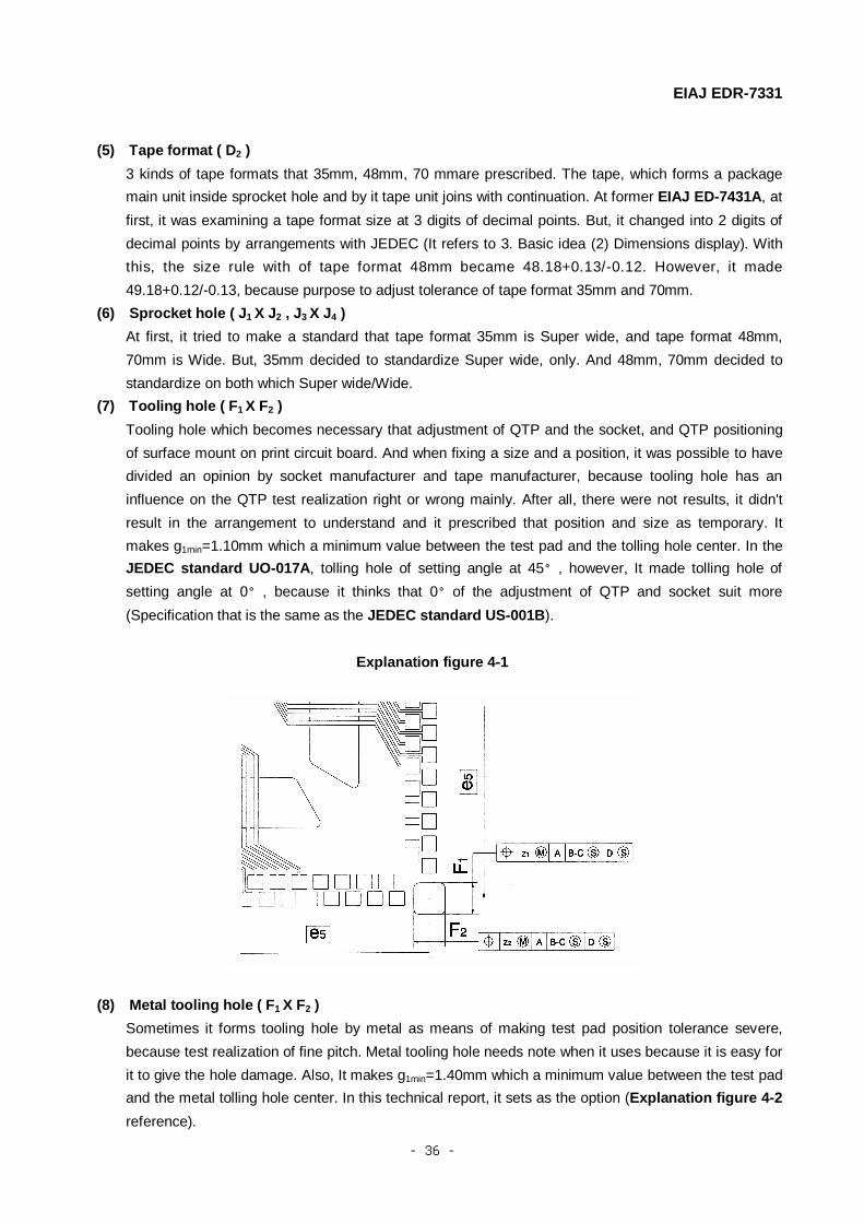
(7) Tooling hole ( F1 X F2 ) Tooling hole which becomes necessary that adjustment of QTP and the socket, and QTP positioning of surface mount on print circuit board. And when fixing a size and a position, it was possible to have divided an opinion by socket manufacturer and tape manufacturer, because tooling hole has an influence on the QTP test realization right or wrong mainly. After all, there were not results, it didn't result in the arrangement to understand and it prescribed that position and size as temporary. It makes g1min=1.10mm which a minimum value between the test pad and the tolling hole center. In the JEDEC standard UO-017A, tolling hole of setting angle at 45°, however, It made tolling hole of setting angle at 0°, because it thinks that 0°of the adjustment of QTP and socket suit more (Specification that is the same as the JEDEC standard US-001B).
Explanation figure 4-1
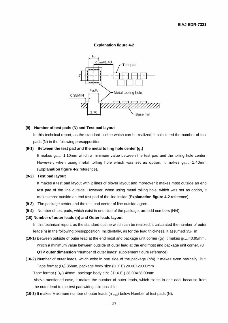
(8) Metal tooling hole ( F1 X F2 ) Sometimes it forms tooling hole by metal as means of making test pad position tolerance severe, because test realization of fine pitch. Metal tooling hole needs note when it uses because it is easy for it to give the hole damage. Also, It makes g1min=1.40mm which a minimum value between the test pad and the metal tolling hole center. In this technical report, it sets as the option (Explanation figure 4-2 reference).
EIAJ EDR-7331
- 37 -
Explanation figure 4-2
g1min=1.40
0.35MIN
1.70
F1xF2
F1
F2
Metal tooling hole
Base film
Test pad
(9) Number of test pads (N) and Test pad layout
In this technical report, as the standard outline which can be realized, it calculated the number of test
pads (N) in the following presupposition.
(9-1) Between the test pad and the metal tolling hole center (g1)
It makes g1min=1.10mm which a minimum value between the test pad and the tolling hole center.
However, when using metal tolling hole which was set as option, it makes g1min=1.40mm
(Explanation figure 4-2 reference).
(9-2) Test pad layout
It makes a test pad layout with 2 lines of plover layout and moreover it makes most outside an end
test pad of the line outside. However, when using metal tolling hole, which was set as option, it
makes most outside an end test pad of the line inside (Explanation figure 4-2 reference).
(9-3) The package center and the test pad center of line outside agree.
(9-4) Number of test pads, which exist in one side of the package, are odd numbers (N/4).
(10) Number of outer leads (n) and Outer leads layout
In this technical report, as the standard outline which can be realized, it calculated the number of outer
leads(n) in the following presupposition. Incidentally, as for the lead thickness, it assumed 35μm.
(10-1) Between outside of outer lead at the end most and package unit corner (g2) It makes g2min=0.95mm,
which a minimum value between outside of outer lead at the end most and package unit corner. (8.
QTP outer dimension “Number of outer leads“ supplement figure reference)
(10-2) Number of outer leads, which exist in one side of the package (n/4) It makes even basically. But,
Tape format (D2) 35mm, package body size (D X E) 20.00X20.00mm
Tape format ( D2 ) 48mm, package body size ( D X E ) 28.00X28.00mm
Above-mentioned case, it makes the number of outer leads, which exists in one odd, because from
the outer lead to the test pad wiring is impossible.
(10-3) It makes Maximum number of outer leads (n max) below Number of test pads (N).
EIAJ EDR-7331
- 38 -
(10-4) It is reduced lead pattern pitch from outer lead to test pad, when there are many number of the
outer leads in bigness of outer lead hole size. In this technical report, It fixed the number of outer
lead, when it makes a lead pattern pitch min 120μm and it made straight part which range of min
0.10mm from inside inner line test pad and reaching of min 0.15mm from outside of outer lead hole.
For number of outer leads details, it refers to 10. Standard Package List.
(11) Index mark width (b1), length (b2)
TCP standards (QTP, DTP(1), DTP(2)) prescribes index mark width with b1=0.15±0.02mm, length
with b2=0.30±0.15mm. It made the same rule which JEDEC standard US-001B. Details are shown
in Explanation figure 4-3.
Explanation figure 4-3
From surface of Cu pattern From surface of film
n-1n
21 1
2
n-1n
b2
b1
The index mark ofn lead can be omitted.
The index mark ofn lead can be omitted.
(12) Number of test pads(N) and Number of outer leads(n)
TCP (QTP, DTP(1), DTP(2)) is a semi-processed article basically and it is impossible to give a
terminal number, considering until jisso process. It follows EIAJ ED-7300 in Number of test pads(N)
and Number of outer leads(n), together. It made a copper foil surface the upper side (From surface of
Cu pattern) and it prescribed the lower left counterclockwise as the 1st. Also, it doesn't use all test
pads. And it gives a number to outer lead and the test pad as follows.
Number of outer leads :1,2,3 …… n
Number of test pads :1,2,3 ……N
(13) Layout of Number of test pads(N) and Number of outer leads(n)
A way of putting the test pad number (N) when forming a tooling hole is shown in explanation figure
4-4. But, corner test pad sometimes belongs to the line inside, when using a metal tooling hole, only.
In this case, it gives a test pad number (N) in the way of being shown in explanation figure 4-5.
However, in case of metal tooling hole, when the corner test pad belongs to the line outside, it follows
explanation figure 4-4.
EIAJ EDR-7331
- 39 -
Layout of Number of test pads( N ) and Number of outer leads( n ) Explanation figure 4-4 Tooling hole Explanation figure 4-5 Metal tooling hole
(From surface of Cu pattern) (From surface of Cu pattern)
N-1
N
2
1
N-2
1.40
N-1
1.40 23
(14) Mouse ear
The lead skew is an important factor. Keeper bar, which leaves polyimide outside the outer lead as the means of improving a lead skew, is effective. Mouse ear which the part to have made extend a part on the outer lead hole, to make it easy to form keeper bar (Explanation figure 4-6 reference).
Explanation figure 4-6
MIN. 0.75mm
MIN
. 1.0
0mm
EIAJ EDR-7331
- 40 -
5. QTP Carrier background for dimensional provisions When QTP carrier was standardized, it prescribed only a basic part about outline and size. It supposed only that it adopted as the reference as the following about the part which depends on the individual specifications such as structure of carrier and that it showed a characteristic.
(1) Structure of QTP Carrier Generally, it is used that 3 typical types are shown below. The characteristic of each type is described as the reference.
(1-1) One peace type It is composed only of main unit and it gets, and it hitches a elasticity notch to the periphery of the tape and it maintains it.
Advantage: It is possible to compose at the low cost. Disadvantage: It is easy for loose tension to occur to the tape because keeping area is limited.
Explanation figure 5-1
(1-2) Two-peace sandwich type
It is composed of two of the main units and the covers and it gets. After insertion tape, it puts in a cover and it lock.
Advantage: It is highly reliable to lock the periphery of the tape uniformly. Disadvantage: A carrier is composed of two, so it is disadvantageous to the cost.
EIAJ EDR-7331
- 41 -
Explanation figure 5-2
本体(main unit)
カバー(cover)
(1-3) Two-peace hinge type
The main unit and the cover be a turning hinge and connect. After insertion tape, it turns and it locks a cover.
Advantage: The treatment is easy. It is highly reliable to lock the periphery of the tape uniformly. Disadvantage: A carrier is composed of two, so it is disadvantageous to the cost.
Explanation figure 5-3
本体(main unit)
ヒンジ(hinge)
カバー(cover)
(2) The positioning of carrier and tape At JEDEC standard CS-006A, It is positioning on sprocket hole of tape and tape locating pin. But, in this technical report, As for the way of positioning a tape, it considered the sharing of the tape, which owns a different sprocket hole and the insert-ability of the tape and it decided not to limit them.
EIAJ EDR-7331
- 42 -
6. The reference standard
(1) IEC standard
Revision of IEC 60191-6 Global drawing format (establishment schedule in 2002)
Amendment 1 to IEC 60191-6 (TSOP(1) and TSOP(2), establishment in 2000) (The related standard,
EIAJ EDR-7312 and EIAJ EDR-7313, establishment in April, 1996)
(2) JEDEC standard
UO-017A (QTP, establishment in October, 1988) (The related standard, CO-009A)
UO-018B (QTP, establishment in July, 1993) (The related standard, EIAJ EDR-7331)
US-001B (QTP, establishment in November, 1993) (The related standard, EIAJ EDR-7331)
CO-009A (QTP Carrier, establishment in July, 1989) (The related standard, UO-017A)
CS-006A (QTP Carrier, establishment in November, 1993) (The related standard, EIAJ EDR-7331)
CS-001B (QTP Carrier magazine, establishment in March, 1996)
(3) JEITA standard
EIAJ EDR-7312 (Design guideline of integrated circuits for Thin Small Outline Package(TypeⅠ),
TSOP(Ⅰ)) , establishment in April, 1996.
EIAJ ED-7311-1 (Standard of integrated circuits package, TSOP(1)) establishment in August, 1997.
EIAJ EDR-7313 (Design guideline of integrated circuits for Thin Small Outline Package(TypeⅡ),
TSOP(Ⅱ)) , establishment in April, 1996.
EIAJ ED-7311-2 (Standard of integrated circuits package, TSOP(2)) establishment in August, 1997.
EIAJ EDR-7332 (Design guideline of integrated circuits for Dual Tape Carrier package Type1, Type2
(DTP (1), DTP (2)), establishment in September, 2002.
EIAJ ED-7303B (Name and Code for Integrated Circuits Package), establishment schedule in 2002.
EIAJ EDR-7331
- 43 -
7. COMMITTEE MEMBERS
The IC Package Sub-committee of the Technical Standardization Committee on Semiconductor Device
Packages has mainly deliberated this standard. The subcommittee members are shown below. <Technical Standardization Committee on Semiconductor Device Package> Chairman SONY CORP. Kazuo Nishiyama < IC Package Sub-committee> Chief MITSUBISHI ELECTRIC CORP. Kazuya Fukuhara Co- chief TOSHIBA CORP. Yasuhiro Koshio HITACHI LTD. Yoshinori Miyaki FUJITSU LTD. Hiroshi Inoue MATSUSHITA ELECTRIC INDUSTRIAL CO., LTD. Tomohiro Tamaki Members AMKOR THECHNOLOGY JAPAN. INC Kazuaki Sorimachi ELPIDA MEMORY, INC. Fumitake Okutsu ENPLAS CORP. Hisao Ohshima OKI ELECTRIC INDUSTRY CO., LTD. Yoshihiko Ino KYOCERA CORP. Akihiro Funahashi SANYO ELECTRIC CORP. Hideyuki Iwamura SANYO ELECTRIC CORP. Kiyoshi Mita SUMITOMO 3M CORP. Akiko Tsubota SEIKO EPSON CORP. Yoshiaki Emoto SONY CORP. Nobuhisa Ishikawa NEC CORP. Kohichi Hirosawa IBM JAPAN CORP. Tsuneo Kobayashi TEXAS INSTRUMENTS JAPAN LTD. Takayuki Ohuchida HITACHI Cable LTD. Tadashi Kawanobe FUJITSU LTD. Shigeyuki Maruyama FUJI ELECTRIC CO., LTD. Osamu Hirohashi MELCO INC. Tsuneo Watanabe YAMAICHI ELECTRONICS CO., LTD. Noriyuki Matsuoka UNITECHNO INC. Hitoshi Matsunaga ROHM CO., LTD. Sadamasa Fujii Special Members iii SHIN-ETSU POLYMER Ken Tamura Special Members iii TOYOJUSHI CO., LTD. ii Hitoshi Kazama <Working Group> Leader h MATSUSHITA ELECTRIC INDUSTRIAL CO., LTD. Toshiyuki Fukuda ELPIDA MEMORY, INC. Fumitake Okutsu Special Members iii TEXAS INSTRUMENTS JAPAN LTD. Takayuki Ohuchida YAMAICHI ELECTRONICS CO., LTD. Noriyuki Matsuoka NEC CORP. Hiroshi Yamanouchi
EIAJ EDR-7331 Published in September, 2002
Published by Technical Standardization Center of Japan Electronics & Information Technology Industries Association 11, Kanda-Surugadai 3-chome, Chiyoda-ku, Tokyo 101-0062, Japan