226
JEDEC SOLID STATE TECHNOLOGY ASSOCIATION JESD79-3E July 2010 JEDEC STANDARD DDR3 SDRAM Specification (Revision of JESD79-3D, August 2009)
JEDEC SOLID STATE TECHNOLOGY ASSOCIATION
JESD79-3E
July 2010
JEDECSTANDARD
DDR3 SDRAM Specification
(Revision of JESD79-3D, August 2009)

NOTICEJEDEC standards and publications contain material that has been prepared, reviewed, andapproved through the JEDEC Board of Directors level and subsequently reviewed and approvedby the JEDEC legal counsel.
JEDEC standards and publications are designed to serve the public interest through eliminatingmisunderstandings between manufacturers and purchasers, facilitating interchangeability andimprovement of products, and assisting the purchaser in selecting and obtaining with minimumdelay the proper product for use by those other than JEDEC members, whether the standard is tobe used either domestically or internationally.
JEDEC standards and publications are adopted without regard to whether or not their adoptionmay involve patents or articles, materials, or processes. By such action JEDEC does not assumeany liability to any patent owner, nor does it assume any obligation whatever to parties adoptingthe JEDEC standards or publications.
The information included in JEDEC standards and publications represents a sound approach toproduct specification and application, principally from the solid state device manufacturerviewpoint. Within the JEDEC organization there are procedures whereby a JEDEC standard orpublication may be further processed and ultimately become an ANSI standard.
No claims to be in conformance with this standard may be made unless all requirements stated inthe standard are met.
Inquiries, comments, and suggestions relative to the content of this JEDEC standard orpublication should be addressed to JEDEC at the address below, or call (703) 907-7559 orwww.jedec.org
Published by
©JEDEC Solid State Technology Association 2010
3103 North 10th Street, Suite 240 South
Arlington, VA 22201
This document may be downloaded free of charge; however JEDEC retains the copyright on thismaterial. By downloading this file the individual agrees not to charge for or resell the resultingmaterial.
PRICE: Please refer to the current
Catalog of JEDEC Engineering Standards and Publications online at
http://www.jedec.org/Catalog/catalog.cfm
Printed in the U.S.A.
All rights reserved
PLEASE!
DON'T VIOLATE THE LAW!
This document is copyrighted by JEDEC and may not bereproduced without permission.
Organizations may obtain permission to reproduce a limited number of copies through entering into a license agreement. For information, contact:
JEDEC Solid State Technology Association3103 North 10th Street, Suite 240 South
Arlington, Virginia 22201or call (703) 907-7559

JEDEC Standard No. 79-3E
1 Scope..........................................................................................................................................12 DDR3 SDRAM Package Pinout and Addressing ......................................................................3
2.1 DDR3 SDRAM x4 Ballout using MO-207........................................................................32.2 DDR3 SDRAM x8 Ballout using MO-207........................................................................42.3 DDR3 SDRAM x16 Ballout using MO-207......................................................................52.4 Stacked / dual-die DDR3 SDRAM x4 Ballout using MO-207..........................................62.5 Stacked / dual-die DDR3 SDRAM x8 Ballout using MO-207..........................................72.6 Stacked / dual-die DDR3 SDRAM x16 Ballout using MO-207........................................82.7 Quad-stacked / Quad-die DDR3 SDRAM x4 Ballout using MO-207...............................92.8 Quad-stacked / Quad-die DDR3 SDRAM x8 Ballout using MO-207.............................102.9 Quad-stacked / Quad-die DDR3 SDRAM x16 Ballout using MO-207...........................112.10 Pinout Description..........................................................................................................132.11 DDR3 SDRAM Addressing...........................................................................................15
2.11.1 512Mb ....................................................................................................................152.11.2 1Gb..........................................................................................................................152.11.3 2Gb .........................................................................................................................152.11.4 4Gb .........................................................................................................................152.11.5 8Gb .........................................................................................................................16
3 Functional Description.............................................................................................................173.1 Simplified State Diagram.................................................................................................173.2 Basic Functionality ..........................................................................................................183.3 RESET and Initialization Procedure ................................................................................19
3.3.1 Power-up Initialization Sequence .............................................................................193.3.2 Reset Initialization with Stable Power......................................................................21
3.4 Register Definition...........................................................................................................223.4.1 Programming the Mode Registers ............................................................................223.4.2 Mode Register MR0..................................................................................................233.4.3 Mode Register MR1..................................................................................................273.4.4 Mode Register MR2..................................................................................................303.4.5 Mode Register MR3..................................................................................................32
4 DDR3 SDRAM Command Description and Operation...........................................................334.1 Command Truth Table .....................................................................................................334.2 CKE Truth Table..............................................................................................................354.3 No OPeration (NOP) Command ......................................................................................364.4 Deselect Command ..........................................................................................................364.5 DLL-off Mode..................................................................................................................374.6 DLL on/off switching procedure......................................................................................38
4.6.1 DLL “on” to DLL “off” Procedure...........................................................................384.6.2 DLL “off” to DLL “on” Procedure...........................................................................39
4.7 Input clock frequency change ..........................................................................................404.8 Write Leveling .................................................................................................................42
4.8.1 DRAM setting for write leveling & DRAM termination function in that mode ......434.8.2 Procedure Description...............................................................................................434.8.3 Write Leveling Mode Exit ........................................................................................45
Contents
i
JEDEC Standard No. 79-3E
4.9 Extended Temperature Usage ..........................................................................................464.9.1 Self-Refresh Temperature Range - SRT...................................................................46
4.10 Multi Purpose Register...................................................................................................484.10.1 MPR Functional Description ..................................................................................494.10.2 MPR Register Address Definition ..........................................................................504.10.3 Relevant Timing Parameters...................................................................................504.10.4 Protocol Example....................................................................................................50
4.11 ACTIVE Command .......................................................................................................554.12 PRECHARGE Command ..............................................................................................554.13 READ Operation............................................................................................................56
4.13.1 READ Burst Operation ...........................................................................................564.13.2 READ Timing Definitions 574.13.3 Burst Read Operation followed by a Precharge......................................................66
4.14 WRITE Operation ..........................................................................................................684.14.1 DDR3 Burst Operation ...........................................................................................684.14.2 WRITE Timing Violations .....................................................................................684.14.3 Write Data Mask .....................................................................................................694.14.4 tWPRE Calculation.................................................................................................704.14.5 tWPST Calculation .................................................................................................70
4.15 Refresh Command..........................................................................................................774.16 Self-Refresh Operation ..................................................................................................794.17 Power-Down Modes ......................................................................................................81
4.17.1 Power-Down Entry and Exit...................................................................................814.17.2 Power-Down clarifications - Case 1 .......................................................................864.17.3 Power-Down clarifications - Case 2 .......................................................................874.17.4 Power-Down clarifications - Case 3 .......................................................................88
4.18 ZQ Calibration Commands ............................................................................................894.18.1 ZQ Calibration Description.....................................................................................894.18.2 ZQ Calibration Timing ...........................................................................................904.18.3 ZQ External Resistor Value, Tolerance, and Capacitive loading ...........................90
5 On-Die Termination (ODT).....................................................................................................915.1 ODT Mode Register and ODT Truth Table.....................................................................915.2 Synchronous ODT Mode .................................................................................................92
5.2.1 ODT Latency and Posted ODT.................................................................................925.2.2 Timing Parameters ....................................................................................................925.2.3 ODT during Reads ....................................................................................................94
5.3 Dynamic ODT..................................................................................................................965.3.1 Functional Description:.............................................................................................965.3.2 ODT Timing Diagrams .............................................................................................97
5.4 Asynchronous ODT Mode .............................................................................................1025.4.1 Synchronous to Asynchronous ODT Mode Transitions.........................................1035.4.2 Synchronous to Asynchronous ODT Mode Transition during
Power-Down Entry .................................................................................................1035.4.3 Asynchronous to Synchronous ODT Mode Transition during
Power-Down Exit ...................................................................................................106
Contents
ii

JEDEC Standard No. 79-3E
5.4.4 Asynchronous to Synchronous ODT Mode during short CKE high and short CKE low periods............................................................................................107
6 Absolute Maximum Ratings ..................................................................................................1096.1 Absolute Maximum DC Ratings....................................................................................1096.2 DRAM Component Operating Temperature Range ......................................................109
7 AC & DC Operating Conditions............................................................................................1117.1 Recommended DC Operating Conditions......................................................................111
8 AC and DC Input Measurement Levels.................................................................................1138.1 AC and DC Logic Input Levels for Single-Ended Signals ............................................113
8.1.1 AC and DC Input Levels for Single-Ended Command and Address Signals.........1138.1.2 AC and DC Input Levels for Single-Ended Data Signals 114
8.2 Vref Tolerances..............................................................................................................1158.3 AC and DC Logic Input Levels for Differential Signals ...............................................116
8.3.1 Differential signal definition...................................................................................1168.3.2 Differential swing requirements for clock (CK - CK#) and strobe
(DQS - DQS#) ........................................................................................................1168.3.3 Single-ended requirements for differential signals .................................................117
8.4 Differential Input Cross Point Voltage ..........................................................................1188.5 Slew Rate Definitions for Single-Ended Input Signals..................................................1208.6 Slew Rate Definitions for Differential Input Signals.....................................................120
9 AC and DC Output Measurement Levels ..............................................................................1229.1 Single Ended AC and DC Output Levels.......................................................................1229.2 Differential AC and DC Output Levels .........................................................................1229.3 Single Ended Output Slew Rate.....................................................................................1239.4 Differential Output Slew Rate........................................................................................1249.5 Reference Load for AC Timing and Output Slew Rate .................................................1259.6 Overshoot and Undershoot Specifications .....................................................................126
9.6.1 Address and Control Overshoot and Undershoot Specifications............................1269.6.2 Clock, Data, Strobe and Mask Overshoot and Undershoot Specifications.............127
9.7 34 ohm Output Driver DC Electrical Characteristics ....................................................1289.7.1 Output Driver Temperature and Voltage sensitivity...............................................129
9.8 On-Die Termination (ODT) Levels and I-V Characteristics .........................................1319.8.1 On-Die Termination (ODT) Levels and I-V Characteristics ..................................1319.8.2 ODT DC Electrical Characteristics.........................................................................1329.8.3 ODT Temperature and Voltage sensitivity .............................................................135
9.9 ODT Timing Definitions................................................................................................1359.9.1 Test Load for ODT Timings ...................................................................................1359.9.2 ODT Timing Definitions.........................................................................................136
10 IDD and IDDQ Specification Parameters and Test Conditions...........................................14010.1 IDD and IDDQ Measurement Conditions ...................................................................14010.2 IDD Specifications .......................................................................................................151
11 Input/Output Capacitance ....................................................................................................15411.1 Input/Output Capacitance ............................................................................................154
Contents
iii
JEDEC Standard No. 79-3E
12 Electrical Characteristics & AC Timing for DDR3-800 to DDR3-2133.............................15712.1 Clock Specification ......................................................................................................157
12.1.1 Definition for tCK(avg) ........................................................................................15712.1.2 Definition for tCK(abs).........................................................................................15712.1.3 Definition for tCH(avg) and tCL(avg)..................................................................15712.1.4 Definition for tJIT(per) and tJIT(per,lck) .............................................................15712.1.5 Definition for tJIT(cc) and tJIT(cc,lck) ................................................................15812.1.6 Definition for tERR(nper).....................................................................................158
12.2 Refresh parameters by device density..........................................................................15812.3 Standard Speed Bins ....................................................................................................159
12.3.1 Speed Bin Table Notes 16713 Electrical Characteristics and AC Timing ...........................................................................169
13.1 Timing Parameters for DDR3-800, DDR3-1067, DDR3-1333, and DDR3-1600.......16913.2 Timing Paramters for DDR3-1866 and DDR3-2133 Speed Bins................................17613.3 Jitter Notes ...................................................................................................................18113.4 Timing Parameter Notes ..............................................................................................18213.5 Address / Command Setup, Hold and Derating...........................................................18413.6 Data Setup, Hold and Slew Rate Derating...................................................................192
Contents
iv
JEDEC Standard No. 79-3E
Figure 1 —Qual-stacked / Quad-die DDR3 SDRAM x4 rank association . . . . . . . . . . . . . . . . . 12Figure 2 —Qual-stacked / Quad-die DDR3 SDRAM x8 rank association . . . . . . . . . . . . . . . . . 12Figure 3 —Qual-stacked / Quad-die DDR3 SDRAM x16 rank association . . . . . . . . . . . . . . . . 12Figure 4 —Simplified State Diagram . . . . . . . . . . . . . . . . . . . . . . . . . . . . . . . . . . . . . . . . . . . . . 17Figure 5 —Reset and Initialization Sequence at Power-on Ramping . . . . . . . . . . . . . . . . . . . . . 20Figure 6 —Reset Procedure at Power Stable Condition . . . . . . . . . . . . . . . . . . . . . . . . . . . . . . . 21Figure 7 —tMRD Timing . . . . . . . . . . . . . . . . . . . . . . . . . . . . . . . . . . . . . . . . . . . . . . . . . . . . . . 22Figure 8 —tMOD Timing . . . . . . . . . . . . . . . . . . . . . . . . . . . . . . . . . . . . . . . . . . . . . . . . . . . . . . 22Figure 9 —MR0 Definition . . . . . . . . . . . . . . . . . . . . . . . . . . . . . . . . . . . . . . . . . . . . . . . . . . . . . 24Figure 10 —MR1 Definition . . . . . . . . . . . . . . . . . . . . . . . . . . . . . . . . . . . . . . . . . . . . . . . . . . . . 27Figure 11 —MR2 Definition . . . . . . . . . . . . . . . . . . . . . . . . . . . . . . . . . . . . . . . . . . . . . . . . . . . . 30Figure 12 —MR3 Definition . . . . . . . . . . . . . . . . . . . . . . . . . . . . . . . . . . . . . . . . . . . . . . . . . . . . 32Figure 13 —DLL-off mode READ Timing Operation . . . . . . . . . . . . . . . . . . . . . . . . . . . . . . . . 37Figure 14 — DLL Switch Sequence from DLL-on to DLL-off . . . . . . . . . . . . . . . . . . . . . . . . . 38Figure 15 —DLL Switch Sequence from DLL Off to DLL On . . . . . . . . . . . . . . . . . . . . . . . . . 39Figure 16 —Change Frequency during Precharge Power-down . . . . . . . . . . . . . . . . . . . . . . . . . 41Figure 17 —Write Leveling Concept . . . . . . . . . . . . . . . . . . . . . . . . . . . . . . . . . . . . . . . . . . . . . 42Figure 18 —Timing details of Write leveling sequence [DQS - DQS# is capturing CK -
CK# low at T1 and CK - CK# high at T2 . . . . . . . . . . . . . . . . . . . . . . . . . . . . . . 44Figure 19 —Timing details of Write leveling exit . . . . . . . . . . . . . . . . . . . . . . . . . . . . . . . . . . . 45Figure 20 —MPR Block Diagram . . . . . . . . . . . . . . . . . . . . . . . . . . . . . . . . . . . . . . . . . . . . . . . . 48Figure 21 —MPR Readout of predefined pattern, BL8 fixed burst order, single readout . . . . . 51Figure 22 —MPR Readout of predefined pattern, BL8 fixed burst order,
back-to-back readout . . . . . . . . . . . . . . . . . . . . . . . . . . . . . . . . . . . . . . . . . . . . . . 52Figure 23 —MPR Readout predefined pattern, BC4, lower nibble then upper nibble . . . . . . . . 53Figure 24 —MPR Readout of predefined pattern, BC4, upper nibble then lower nibble . . . . . . 54Figure 25 —READ Burst Operation RL = 5 (AL = 0, CL = 5, BL8) . . . . . . . . . . . . . . . . . . . . . 56Figure 26 —READ Burst Operation RL = 9 (AL = 4, CL = 5, BL8) . . . . . . . . . . . . . . . . . . . . . 56Figure 27 —READ Timing Definition . . . . . . . . . . . . . . . . . . . . . . . . . . . . . . . . . . . . . . . . . . . . 57Figure 28 —Clock to Data Strobe Relationship . . . . . . . . . . . . . . . . . . . . . . . . . . . . . . . . . . . . . 58Figure 29 —Data Strobe to Data Relationship . . . . . . . . . . . . . . . . . . . . . . . . . . . . . . . . . . . . . . 59Figure 30 —tLZ and tHZ method for calculating transitions and endpoints . . . . . . . . . . . . . . . . 60Figure 31 —Method for calculating tRPRE transitions and endpoints . . . . . . . . . . . . . . . . . . . . 61Figure 32 —Method for calculating tRPST transitions and endpoints . . . . . . . . . . . . . . . . . . . . 61Figure 33 —READ (BL8) to READ (BL8) . . . . . . . . . . . . . . . . . . . . . . . . . . . . . . . . . . . . . . . . . 62Figure 34 —Nonconsecutive READ (BL8) to READ (BL8), tCCD=5 . . . . . . . . . . . . . . . . . . . 62Figure 35 —READ (BC4) to READ (BC4) . . . . . . . . . . . . . . . . . . . . . . . . . . . . . . . . . . . . . . . . 63Figure 36 —READ (BL8) to WRITE (BL8) . . . . . . . . . . . . . . . . . . . . . . . . . . . . . . . . . . . . . . . . 63Figure 37 —READ (BC4) to WRITE (BC4) OTF . . . . . . . . . . . . . . . . . . . . . . . . . . . . . . . . . . . 64Figure 38 —READ (BL8) to READ (BC4) OTF . . . . . . . . . . . . . . . . . . . . . . . . . . . . . . . . . . . . 64Figure 39 —READ (BC4) to READ (BL8) OTF . . . . . . . . . . . . . . . . . . . . . . . . . . . . . . . . . . . . 65Figure 40 —READ (BC4) to WRITE (BL8) OTF . . . . . . . . . . . . . . . . . . . . . . . . . . . . . . . . . . . 65Figure 41 —READ (BL8) to WRITE (BC4) OTF . . . . . . . . . . . . . . . . . . . . . . . . . . . . . . . . . . . 66Figure 42 —READ to PRECHARGE, RL = 5, AL = 0, CL = 5, tRTP = 4, tRP = 5 . . . . . . . . . 67Figure 43 —READ to PRECHARGE, RL = 8, AL = CL-2, CL = 5, tRTP = 6, tRP = 5 . . . . . . 67Figure 44 —Write Timing Definition and Parameters . . . . . . . . . . . . . . . . . . . . . . . . . . . . . . . . 69Figure 45 —Method for calculating tWPRE transitions and endpoints . . . . . . . . . . . . . . . . . . . 70Figure 46 —Method for calculating tWPST transitions and endpoints . . . . . . . . . . . . . . . . . . . . 70
List of Figures
v
JEDEC Standard No. 79-3E
Figure 47 —WRITE Burst Operation WL = 5 (AL = 0, CWL = 5, BL8) . . . . . . . . . . . . . . . . . . 71Figure 48 —WRITE Burst Operation WL = 9 (AL = CL-1, CWL = 5, BL8) . . . . . . . . . . . . . . 71Figure 49 —WRITE (BC4) to READ (BC4) Operation . . . . . . . . . . . . . . . . . . . . . . . . . . . . . . . 72Figure 50 —WRITE (BC4) to PRECHARGE Operation . . . . . . . . . . . . . . . . . . . . . . . . . . . . . . 72Figure 51 —WRITE (BC4) OTF to PRECHARGE Operation . . . . . . . . . . . . . . . . . . . . . . . . . . 72Figure 52 —WRITE (BL8) to WRITE (BL8) . . . . . . . . . . . . . . . . . . . . . . . . . . . . . . . . . . . . . . . 73Figure 53 —WRITE (BC4) to WRITE (BC4) OTF . . . . . . . . . . . . . . . . . . . . . . . . . . . . . . . . . . 73Figure 54 —WRITE (BL8) to READ (BC4/BL8) OTF . . . . . . . . . . . . . . . . . . . . . . . . . . . . . . . 74Figure 55 —WRITE (BC4) to READ (BC4/BL8) OTF . . . . . . . . . . . . . . . . . . . . . . . . . . . . . . . 74Figure 56 —WRITE (BC4) to READ (BC4) . . . . . . . . . . . . . . . . . . . . . . . . . . . . . . . . . . . . . . . 75Figure 57 —WRITE (BL8) to WRITE (BC4) OTF . . . . . . . . . . . . . . . . . . . . . . . . . . . . . . . . . . 75Figure 58 —WRITE (BC4) to WRITE (BL8) OTF . . . . . . . . . . . . . . . . . . . . . . . . . . . . . . . . . . 76Figure 59 —Refresh Command Timing . . . . . . . . . . . . . . . . . . . . . . . . . . . . . . . . . . . . . . . . . . . 77Figure 60 —Postponing Refresh Commands (Example) . . . . . . . . . . . . . . . . . . . . . . . . . . . . . . 77Figure 61 —Pulling-in Refresh Commands (Example) . . . . . . . . . . . . . . . . . . . . . . . . . . . . . . . 78Figure 62 —Self-Refresh Entry/Exit Timing . . . . . . . . . . . . . . . . . . . . . . . . . . . . . . . . . . . . . . . 80Figure 63 —Active Power-Down Entry and Exit Timing Diagram . . . . . . . . . . . . . . . . . . . . . . 82Figure 64 —Power-Down Entry after Read and Read with Auto Precharge . . . . . . . . . . . . . . . 82Figure 65 —Power-Down Entry after Write with Auto Precharge . . . . . . . . . . . . . . . . . . . . . . . 83Figure 66 —Power-Down Entry after Write . . . . . . . . . . . . . . . . . . . . . . . . . . . . . . . . . . . . . . . . 83Figure 67 —Precharge Power-Down (Fast Exit Mode) Entry and Exit . . . . . . . . . . . . . . . . . . . 84Figure 68 — Precharge Power-Down (Slow Exit Mode) Entry and Exit . . . . . . . . . . . . . . . . . . 84Figure 69 — Refresh Command to Power-Down Entry . . . . . . . . . . . . . . . . . . . . . . . . . . . . . . . 85Figure 70 — Active Command to Power-Down Entry . . . . . . . . . . . . . . . . . . . . . . . . . . . . . . . . 85Figure 71 — Precharge / Precharge all Command to Power-Down Entry . . . . . . . . . . . . . . . . . 86Figure 72 — MRS Command to Power-Down Entry . . . . . . . . . . . . . . . . . . . . . . . . . . . . . . . . . 86Figure 73 —Power-Down Entry/Exit Clarifications - Case 1 . . . . . . . . . . . . . . . . . . . . . . . . . . . 87Figure 74 —Power-Down Entry/Exit Clarifications - Case 2 . . . . . . . . . . . . . . . . . . . . . . . . . . . 87Figure 75 —Power-Down Entry/Exit Clarifications - Case 3 . . . . . . . . . . . . . . . . . . . . . . . . . . . 88Figure 76 —ZQ Calibration Timing . . . . . . . . . . . . . . . . . . . . . . . . . . . . . . . . . . . . . . . . . . . . . . 90Figure 77 —Functional Representation of ODT . . . . . . . . . . . . . . . . . . . . . . . . . . . . . . . . . . . . . 91Figure 78 —Synchronous ODT Timing Example for AL = 3; CWL = 5; ODTLon =
AL + CWL - 2 = 6.0; ODTLoff = AL + CWL - 2 = 6 . . . . . . . . . . . . . . . . . . . . . 93Figure 79 —Synchronous ODT example with BL = 4, WL = 7. . . . . . . . . . . . . . . . . . . . . . . . . 94Figure 80 —ODT must be disabled externally during Reads by driving ODT low.
(example: CL = 6; AL = CL - 1 = 5; RL = AL + CL = 11; CWL = 5; ODTLon = CWL + AL - 2 = 8; ODTLoff = CWL + AL - 2 = 8) . . . . . . . . . . . . 95
Figure 81 —Dynamic ODT: Behavior with ODT being asserted before and after the write . . . 98Figure 82 —Dynamic ODT: Behavior without write command, AL = 0, CWL = 5 . . . . . . . . . 98Figure 83 —Dynamic ODT: Behavior with ODT pin being asserted together with write
command for a duration of 6 clock cycles . . . . . . . . . . . . . . . . . . . . . . . . . . . . . . 99Figure 84 —Dynamic ODT: Behavior with ODT pin being asserted together with write
command for a duration of 6 clock cycles, example for BC4 (via MRS or OTF), AL = 0, CWL = 5. . . . . . . . . . . . . . . . . . . . . . . . . . . . . . . . . . . . . . . . . . . 100
Figure 85 —Dynamic ODT: Behavior with ODT pin being asserted together with write command for a duration of 4 clock cycles . . . . . . . . . . . . . . . . . . . . . . . . . . . . . 101
Figure 86 —Asynchronous ODT Timings on DDR3 SDRAM with fast ODT transition: AL is ignored . . . . . . . . . . . . . . . . . . . . . . . . . . . . . . . . . . . . . . . . . . 102
List of Figures
vi

JEDEC Standard No. 79-3E
Figure 87 —Synchronous to asynchronous transition during Precharge Power Down (with DLL frozen) entry (AL = 0; CWL = 5; tANPD = WL - 1 = 4) . . . . . . . . 104
Figure 88 —Synchronous to asynchronous transition after Refresh command (AL = 0; CWL = 5; tANPD = WL - 1 = 4) . . . . . . . . . . . . . . . . . . . . . . . . . . . . . . . . . . . . 105
Figure 89 —Asynchronous to synchronous transition during Precharge Power Down (with DLL frozen) exit (CL = 6; AL = CL - 1; CWL = 5; tANPD = WL - 1 = 9) . . . . . . . . . . . . . . . . . . . . . . . . . . . . . . . . . . . . . . . . . . . . . . . . . . . . 106
Figure 90 —Transition period for short CKE cycles, entry and exit period overlapping (AL = 0, WL = 5, tANPD = WL - 1 = 4) . . . . . . . . . . . . . . . . . . . . . . . . . . . . . . 107
Figure 91 —Illustration of VRef(DC) tolerance and VRef ac-noise limits . . . . . . . . . . . . . . . . 115Figure 92 —Definition of differential ac-swing and “time above ac-level” tDVAC . . . . . . . . 116Figure 93 —Single-ended requirement for differential signals. . . . . . . . . . . . . . . . . . . . . . . . . 118Figure 94 —Vix Definition . . . . . . . . . . . . . . . . . . . . . . . . . . . . . . . . . . . . . . . . . . . . . . . . . . . . 119Figure 95 —Differential Input Slew Rate Definition for DQS, DQS# and CK, CK# . . . . . . . . 120Figure 96 —Single-ended Output Slew Rate Definition . . . . . . . . . . . . . . . . . . . . . . . . . . . . . . 123Figure 97 —Differential Output Slew Rate Definition . . . . . . . . . . . . . . . . . . . . . . . . . . . . . . . 124Figure 98 —Reference Load for AC Timing and Output Slew Rate . . . . . . . . . . . . . . . . . . . . 125Figure 99 —Address and Control Overshoot and Undershoot Definition . . . . . . . . . . . . . . . . 126Figure 100 —Clock, Data, Strobe and Mask Overshoot and Undershoot Definition . . . . . . . . 127Figure 101 —Output Driver: Definition of Voltages and Currents . . . . . . . . . . . . . . . . . . . . . . 128Figure 102 —On-Die Termination: Definition of Voltages and Currents . . . . . . . . . . . . . . . . . 131Figure 103 —ODT Timing Reference Load . . . . . . . . . . . . . . . . . . . . . . . . . . . . . . . . . . . . . . . 135Figure 104 —Definition of tAON . . . . . . . . . . . . . . . . . . . . . . . . . . . . . . . . . . . . . . . . . . . . . . . . . 137Figure 105 —Definition of tAONPD . . . . . . . . . . . . . . . . . . . . . . . . . . . . . . . . . . . . . . . . . . . . . . . 137Figure 106 —Definition of tAOF . . . . . . . . . . . . . . . . . . . . . . . . . . . . . . . . . . . . . . . . . . . . . . . . . 138Figure 107 —Definition of tAOFPD . . . . . . . . . . . . . . . . . . . . . . . . . . . . . . . . . . . . . . . . . . . . . . . 138Figure 108 —Definition of tADC . . . . . . . . . . . . . . . . . . . . . . . . . . . . . . . . . . . . . . . . . . . . . . . . . 139Figure 109 — Measurement Setup and Test Load for IDD and IDDQ
(optional) Measurements . . . . . . . . . . . . . . . . . . . . . . . . . . . . . . . . . . . . . . . . . . 141Figure 110 —Correlation from simulated Channel IO Power to actual Channel IO Power
supported by IDDQ Measurement. . . . . . . . . . . . . . . . . . . . . . . . . . . . . . . . . . . 141Figure 111 —Illustration of nominal slew rate and tVAC for setup time tIS (for ADD/CMD
with respect to clock). . . . . . . . . . . . . . . . . . . . . . . . . . . . . . . . . . . . . . . . . . . . . 188Figure 112 —Illustration of nominal slew rate for hold time tIH (for ADD/CMD with
respect to clock). . . . . . . . . . . . . . . . . . . . . . . . . . . . . . . . . . . . . . . . . . . . . . . . . 189Figure 113 —Illustration of tangent line for setup time tIS (for ADD/CMD with
respect to clock) . . . . . . . . . . . . . . . . . . . . . . . . . . . . . . . . . . . . . . . . . . . . . . . . . 190Figure 114 —Illustration of tangent line for for hold time tIH (for ADD/CMD with
respect to clock) . . . . . . . . . . . . . . . . . . . . . . . . . . . . . . . . . . . . . . . . . . . . . . . . . 191Figure 115 —Illustration of nominal slew rate and tVAC for setup time tDS (for DQ
with respect to strobe) . . . . . . . . . . . . . . . . . . . . . . . . . . . . . . . . . . . . . . . . . . . . 196Figure 116 —Illustration of nominal slew rate for hold time tDH (for DQ with
respect to strobe) . . . . . . . . . . . . . . . . . . . . . . . . . . . . . . . . . . . . . . . . . . . . . . . . 197Figure 117 —Illustration of tangent line for setup time tDS (for DQ with respect to strobe) . . 198Figure 118 —Illustration of tangent line for for hold time tDH (for DQ
with respect to strobe) . . . . . . . . . . . . . . . . . . . . . . . . . . . . . . . . . . . . . . . . . . . . 199
List of Figures
vii
JEDEC Standard No. 79-3E
Table 1 —Input/output functional description . . . . . . . . . . . . . . . . . . . . . . . . . . . . . . . . . . . . . . . 13Table 2 —State Diagram Command Definitions . . . . . . . . . . . . . . . . . . . . . . . . . . . . . . . . . . . . . 17Table 3 —Burst Type and Burst Order. . . . . . . . . . . . . . . . . . . . . . . . . . . . . . . . . . . . . . . . . . . . . 25Table 4 —Additive Latency (AL) Settings. . . . . . . . . . . . . . . . . . . . . . . . . . . . . . . . . . . . . . . . . . 28Table 5 —TDQS, TDQS# Function Matrix . . . . . . . . . . . . . . . . . . . . . . . . . . . . . . . . . . . . . . . . . 29Table 6 —Command Truth Table. . . . . . . . . . . . . . . . . . . . . . . . . . . . . . . . . . . . . . . . . . . . . . . . . 33Table 7 —CKE Truth Table . . . . . . . . . . . . . . . . . . . . . . . . . . . . . . . . . . . . . . . . . . . . . . . . . . . . . 35Table 8 —MR setting involved in the leveling procedure . . . . . . . . . . . . . . . . . . . . . . . . . . . . . . 43Table 9 —DRAM termination function in the leveling mode . . . . . . . . . . . . . . . . . . . . . . . . . . . 43Table 10 —Mode Register Description . . . . . . . . . . . . . . . . . . . . . . . . . . . . . . . . . . . . . . . . . . . . 46Table 11 —Self-Refresh mode summary . . . . . . . . . . . . . . . . . . . . . . . . . . . . . . . . . . . . . . . . . . . 47Table 12 —MPR MR3 Register Definition . . . . . . . . . . . . . . . . . . . . . . . . . . . . . . . . . . . . . . . . . 48Table 13 —MPR MR3 Register Definition . . . . . . . . . . . . . . . . . . . . . . . . . . . . . . . . . . . . . . . . . 50Table 14 —Power-Down Entry Definitions . . . . . . . . . . . . . . . . . . . . . . . . . . . . . . . . . . . . . . . . . 81Table 15 —Termination Truth Table . . . . . . . . . . . . . . . . . . . . . . . . . . . . . . . . . . . . . . . . . . . . . . 91Table 16 —Latencies and timing parameters relevant for Dynamic ODT. . . . . . . . . . . . . . . . . . 96Table 17 —Timing Diagrams for “Dynamic ODT”. . . . . . . . . . . . . . . . . . . . . . . . . . . . . . . . . . . 97Table 18 —Asynchronous ODT Timing Parameters for all Speed Bins . . . . . . . . . . . . . . . . . . 102Table 19 —ODT timing parameters for Power Down (with DLL frozen) entry and
exit transition period . . . . . . . . . . . . . . . . . . . . . . . . . . . . . . . . . . . . . . . . . . . . . . . . . . . . . . . 103Table 20 —Absolute Maximum DC Ratings . . . . . . . . . . . . . . . . . . . . . . . . . . . . . . . . . . . . . . . 109Table 21 —Temperature Range . . . . . . . . . . . . . . . . . . . . . . . . . . . . . . . . . . . . . . . . . . . . . . . . . 109Table 22 —Recommended DC Operating Conditions . . . . . . . . . . . . . . . . . . . . . . . . . . . . . . . . 111Table 23 —Single-Ended AC and DC Input Levels for Command and Address . . . . . . . . . . . 113Table 24 —Single-Ended AC and DC Input Levels for DQ and DM . . . . . . . . . . . . . . . . . . . . 114Table 25 —Differential AC and DC Input Levels . . . . . . . . . . . . . . . . . . . . . . . . . . . . . . . . . . . 116Table 26 —Allowed time before ringback (tDVAC) for CK - CK# and DQS - DQS#. . . . . . . 117Table 27 —Single-ended levels for CK, DQS, DQSL, DQSU, CK#, DQS#,
DQSL# or DQSU# . . . . . . . . . . . . . . . . . . . . . . . . . . . . . . . . . . . . . . . . . . . . . . . . . . . . . . . . 118Table 28 —Cross point voltage for differential input signals (CK, DQS) . . . . . . . . . . . . . . . . . 119Table 29 —Differential Input Slew Rate Definition . . . . . . . . . . . . . . . . . . . . . . . . . . . . . . . . . 120Table 30 —Single-ended AC and DC Output Levels. . . . . . . . . . . . . . . . . . . . . . . . . . . . . . . . . 122Table 31 —Differential AC and DC Output Levels . . . . . . . . . . . . . . . . . . . . . . . . . . . . . . . . . . 122Table 32 —Single-ended Output Slew Rate Definition . . . . . . . . . . . . . . . . . . . . . . . . . . . . . . 123Table 33 —Output Slew Rate (Single-ended) . . . . . . . . . . . . . . . . . . . . . . . . . . . . . . . . . . . . . . 123Table 34 —Differential Output Slew Rate Definition . . . . . . . . . . . . . . . . . . . . . . . . . . . . . . . . 124Table 35 —Differential Output Slew Rate . . . . . . . . . . . . . . . . . . . . . . . . . . . . . . . . . . . . . . . . . 124Table 36 —AC Overshoot/Undershoot Specification for Address and Control Pins. . . . . . . . . 126Table 37 —AC Overshoot/Undershoot Specification for Clock, Data, Strobe and Mask . . . . . 127Table 38 —Output Driver DC Electrical Characteristics, assuming RZQ = 240 W ;
entire operating temperature range; after proper ZQ calibration . . . . . . . . . . . . . . . . . . . . . 129Table 39 —Output Driver Sensitivity Definition . . . . . . . . . . . . . . . . . . . . . . . . . . . . . . . . . . . . 130Table 40 —Output Driver Voltage and Temperature Sensitivity. . . . . . . . . . . . . . . . . . . . . . . . 130Table 41 —ODT DC Electrical Characteristics, assuming RZQ = 240 W +/- 1%
entire operating temperature range; after proper ZQ calibration . . . . . . . . . . . . . . . . . . . . . 132
List of Tables
viii

JEDEC Standard No. 79-3E
Table 42 —ODT Sensitivity Definition . . . . . . . . . . . . . . . . . . . . . . . . . . . . . . . . . . . . . . . . . . . 135Table 43 —ODT Voltage and Temperature Sensitivity . . . . . . . . . . . . . . . . . . . . . . . . . . . . . . . 135Table 44 —ODT Timing Definitions . . . . . . . . . . . . . . . . . . . . . . . . . . . . . . . . . . . . . . . . . . . . . 136Table 45 —Reference Settings for ODT Timing Measurements . . . . . . . . . . . . . . . . . . . . . . . . 136Table 46 —Timings used for IDD and IDDQ Measurement-Loop Patterns
for 800/1066/1333/1600 . . . . . . . . . . . . . . . . . . . . . . . . . . . . . . . . . . . . . . . . . . . . . . . . . . . . 142Table 47 —Timings used for IDD and IDDQ Measurement-Loop Patterns for 1866/2133 . . . 142Table 48 —Basic IDD and IDDQ Measurement Conditions . . . . . . . . . . . . . . . . . . . . . . . . . . . 143Table 49 —IDD0 Measurement-Loop Pattern . . . . . . . . . . . . . . . . . . . . . . . . . . . . . . . . . . . . . . 145Table 50 —IDD1 Measurement-Loop Pattern . . . . . . . . . . . . . . . . . . . . . . . . . . . . . . . . . . . . . . 146Table 51 —IDD2N and IDD3N Measurement-Loop Pattern. . . . . . . . . . . . . . . . . . . . . . . . . . . 147Table 52 —IDD2NT and IDDQ2NT Measurement-Loop Pattern . . . . . . . . . . . . . . . . . . . . . . . 147Table 53 —IDD4R and IDDQ4R Measurement-Loop Pattern . . . . . . . . . . . . . . . . . . . . . . . . . 148Table 54 —IDD4W Measurement-Loop Pattern . . . . . . . . . . . . . . . . . . . . . . . . . . . . . . . . . . . . 148Table 55 —IDD5B Measurement-Loop Pattern. . . . . . . . . . . . . . . . . . . . . . . . . . . . . . . . . . . . . 149Table 56 —IDD7 Measurement-Loop Pattern . . . . . . . . . . . . . . . . . . . . . . . . . . . . . . . . . . . . . . 150Table 57 —IDD Specification Example 512M DDR3. . . . . . . . . . . . . . . . . . . . . . . . . . . . . . . . . 151Table 58 —IDD6 Specification. . . . . . . . . . . . . . . . . . . . . . . . . . . . . . . . . . . . . . . . . . . . . . . . . . . 152Table 59 —800/1066/1333/1600 Input / Output Capacitance . . . . . . . . . . . . . . . . . . . . . . . . . . 154Table 60 —1866/2133 Input / Output Capacitance . . . . . . . . . . . . . . . . . . . . . . . . . . . . . . . . . . 155Table 61 —Refresh parameters by device density . . . . . . . . . . . . . . . . . . . . . . . . . . . . . . . . . . . 158Table 62 —DDR3-800 Speed Bins and Operating Conditions . . . . . . . . . . . . . . . . . . . . . . . . . 159Table 63 —DDR3-1066 Speed Bins and Operating Conditions . . . . . . . . . . . . . . . . . . . . . . . . 160Table 64 —DDR3-1333 Speed Bins and Operating Conditions . . . . . . . . . . . . . . . . . . . . . . . . 161Table 65 —DDR3-1600 Speed Bins and Operating Conditions . . . . . . . . . . . . . . . . . . . . . . . . 162Table 66 —DDR3-1866 Speed Bins and Operating Conditions . . . . . . . . . . . . . . . . . . . . . . . . 164Table 67 —DDR3-2133 Speed Bins and Operating Conditions . . . . . . . . . . . . . . . . . . . . . . . . 165Table 69 —Timing Parameters by Speed Bin . . . . . . . . . . . . . . . . . . . . . . . . . . . . . . . . . . . . . . 176Table 70 —ADD/CMD Setup and Hold Base-Values for 1V/ns . . . . . . . . . . . . . . . . . . . . . . . 184Table 71 —Derating values DDR3-800/1066/1333/1600 tIS/tIH - ac/dc based
AC175 Threshold . . . . . . . . . . . . . . . . . . . . . . . . . . . . . . . . . . . . . . . . . . . . . . . . . . . . . . . . . 185Table 72 —Derating values DDR3-800/1066/1333/1600 tIS/tIH - ac/dc based -
Alternate AC150 Threshold . . . . . . . . . . . . . . . . . . . . . . . . . . . . . . . . . . . . . . . . . . . . . . . . . 185Table 73 —Derating values DDR3-1866/2133 tIS/tIH - ac/dc based
Alternate AC135 Threshold . . . . . . . . . . . . . . . . . . . . . . . . . . . . . . . . . . . . . . . . . . . . . . . . . 186Table 74 —Derating values DDR3-1866/2133 tIS/tIH - ac/dc based
Alternate AC125 Threshold186Table 75 —Required time tVAC above VIH(ac) {below VIL(ac)} for valid
ADD/CMD transition . . . . . . . . . . . . . . . . . . . . . . . . . . . . . . . . . . . . . . . . . . . . . . . . . . . . . . 187Table 76 —Data Setup and Hold Base-Values . . . . . . . . . . . . . . . . . . . . . . . . . . . . . . . . . . . . . 192Table 77 —Derating values DDR3-800/1066 tDS/tDH - (AC175) . . . . . . . . . . . . . . . . . . . . . . 193Table 78 —Derating values for DDR3-800/1066/1333/1600 tDS/tDH - (AC150)Derating . . . 193Table 79 —Derating values for DDR3-1866/2133 tDS/tDH - (AC135) . . . . . . . . . . . . . . . . . . 194Table 80 —Required time tVAC above VIH(ac) {below VIL(ac)} for valid DQ transition . . . 195
List of Tables
ix

JEDEC Standard No. 79-3E
This page left blank.
x

JEDEC Standard No. 79-3EPage 1
1 ScopeThis document defines the DDR3 SDRAM specification, including features, functionalities, AC and DC characteristics, packages, and ball/signal assignments. The purpose of this Specification is to define the minimum set of requirements for JEDEC compliant 512 Mb through 8 Gb for x4, x8, and x16 DDR3 SDRAM devices. This specification was created based on the DDR2 specification (JESD79-2) and some aspects of the DDR specification (JESD79). Each aspect of the changes for DDR3 SDRAM operation were considered and approved by committee ballot(s). The accumulation of these ballots were then incorporated to prepare this JESD79-3 specification, replacing whole sections and incorporating the changes into Functional Description and Operation.

JEDEC Standard No. 79-3EPage 2
This page left blank.
JEDEC Standard No. 79-3EPage 3
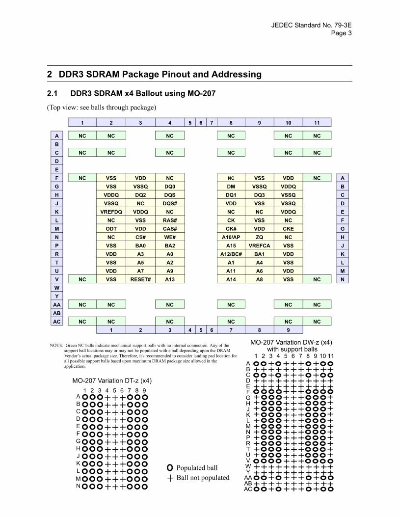
2 DDR3 SDRAM Package Pinout and Addressing
2.1 DDR3 SDRAM x4 Ballout using MO-207
(Top view: see balls through package)
1 2 3 4 5 6 7 8 9 10 11
A NC NC NC NC NC NCBC NC NC NC NC NC NCDEF NC VSS VDD NC NC VSS VDD NC AG VSS VSSQ DQ0 DM VSSQ VDDQ BH VDDQ DQ2 DQS DQ1 DQ3 VSSQ CJ VSSQ NC DQS# VDD VSS VSSQ DK VREFDQ VDDQ NC NC NC VDDQ EL NC VSS RAS# CK VSS NC FM ODT VDD CAS# CK# VDD CKE GN NC CS# WE# A10/AP ZQ NC HP VSS BA0 BA2 A15 VREFCA VSS JR VDD A3 A0 A12/BC# BA1 VDD KT VSS A5 A2 A1 A4 VSS LU VDD A7 A9 A11 A6 VDD MV NC VSS RESET# A13 A14 A8 VSS NC NWY
AA NC NC NC NC NC NCABAC NC NC NC NC NC NC
1 2 3 4 5 6 7 8 9
1 2 3 4 8 95 6 7ABCDEFGHJKL
MO-207 Variation DT-z (x4)
Populated ballBall not populated
NM
1 2 3 4 8 95 6 7ABCDEFGHJKL
MO-207 Variation DW-z (x4)
NM
10 11
PRTUVWY
AAABAC
with support ballsNOTE: Green NC balls indicate mechanical support balls with no internal connection. Any of the
support ball locations may or may not be populated with a ball depending upon the DRAM Vendor’s actual package size. Therefore, it's recommended to consider landing pad location for all possible support balls based upon maximum DRAM package size allowed in the application.
JEDEC Standard No. 79-3EPage 4
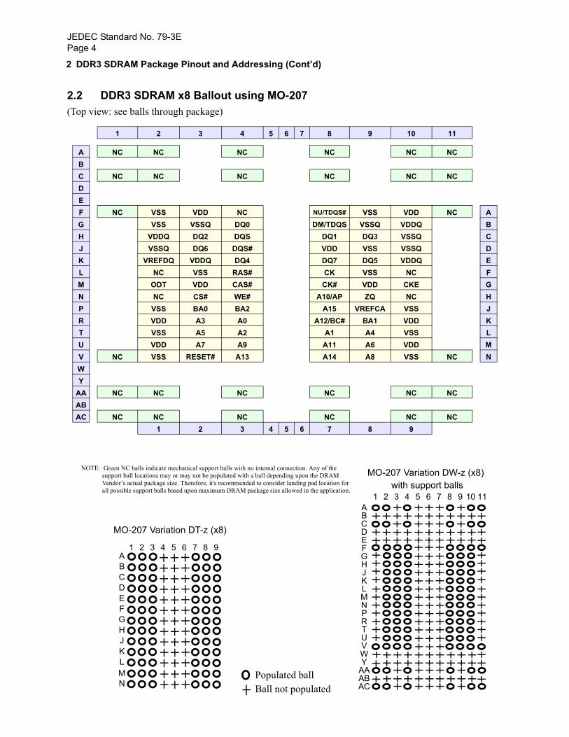
2 DDR3 SDRAM Package Pinout and Addressing (Cont’d)
2.2 DDR3 SDRAM x8 Ballout using MO-207 (Top view: see balls through package)
1 2 3 4 5 6 7 8 9 10 11
A NC NC NC NC NC NCBC NC NC NC NC NC NCDEF NC VSS VDD NC NU/TDQS# VSS VDD NC AG VSS VSSQ DQ0 DM/TDQS VSSQ VDDQ BH VDDQ DQ2 DQS DQ1 DQ3 VSSQ CJ VSSQ DQ6 DQS# VDD VSS VSSQ DK VREFDQ VDDQ DQ4 DQ7 DQ5 VDDQ EL NC VSS RAS# CK VSS NC FM ODT VDD CAS# CK# VDD CKE GN NC CS# WE# A10/AP ZQ NC HP VSS BA0 BA2 A15 VREFCA VSS JR VDD A3 A0 A12/BC# BA1 VDD KT VSS A5 A2 A1 A4 VSS LU VDD A7 A9 A11 A6 VDD MV NC VSS RESET# A13 A14 A8 VSS NC NWY
AA NC NC NC NC NC NCABAC NC NC NC NC NC NC
1 2 3 4 5 6 7 8 9
1 2 3 4 8 95 6 7ABCDEFGHJKL
MO-207 Variation DT-z (x8)
NM
1 2 3 4 8 95 6 7ABCDEFGHJKL
MO-207 Variation DW-z (x8)
NM
10 11
PRTUVWY
AAABAC
with support balls
NOTE: Green NC balls indicate mechanical support balls with no internal connection. Any of the support ball locations may or may not be populated with a ball depending upon the DRAM Vendor’s actual package size. Therefore, it's recommended to consider landing pad location for all possible support balls based upon maximum DRAM package size allowed in the application.
Populated ballBall not populated
JEDEC Standard No. 79-3EPage 5
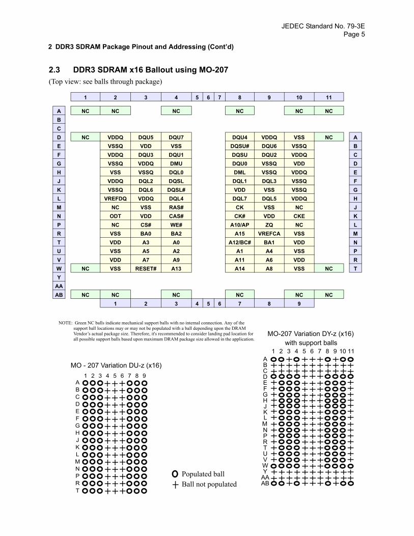
2 DDR3 SDRAM Package Pinout and Addressing (Cont’d)
2.3 DDR3 SDRAM x16 Ballout using MO-207 (Top view: see balls through package)
1 2 3 4 5 6 7 8 9 10 11
A NC NC NC NC NC NCBCD NC VDDQ DQU5 DQU7 DQU4 VDDQ VSS NC AE VSSQ VDD VSS DQSU# DQU6 VSSQ BF VDDQ DQU3 DQU1 DQSU DQU2 VDDQ CG VSSQ VDDQ DMU DQU0 VSSQ VDD DH VSS VSSQ DQL0 DML VSSQ VDDQ EJ VDDQ DQL2 DQSL DQL1 DQL3 VSSQ FK VSSQ DQL6 DQSL# VDD VSS VSSQ GL VREFDQ VDDQ DQL4 DQL7 DQL5 VDDQ HM NC VSS RAS# CK VSS NC JN ODT VDD CAS# CK# VDD CKE KP NC CS# WE# A10/AP ZQ NC LR VSS BA0 BA2 A15 VREFCA VSS MT VDD A3 A0 A12/BC# BA1 VDD NU VSS A5 A2 A1 A4 VSS PV VDD A7 A9 A11 A6 VDD RW NC VSS RESET# A13 A14 A8 VSS NC TY
AAAB NC NC NC NC NC NC
1 2 3 4 5 6 7 8 9
1 2 3 4 8 95 6 7ABCDEFGHJ
MO-207 Variation DY-z (x16)
N
10 11
PRTUVWY
AAAB
with support balls
1 2 3 4 8 95 6 7ABCDEFGHJKLMNPR
MO - 207 Variation DU-z (x16)
T
KLM
Populated ballBall not populated
NOTE: Green NC balls indicate mechanical support balls with no internal connection. Any of the support ball locations may or may not be populated with a ball depending upon the DRAM Vendor’s actual package size. Therefore, it's recommended to consider landing pad location for all possible support balls based upon maximum DRAM package size allowed in the application.
JEDEC Standard No. 79-3EPage 6
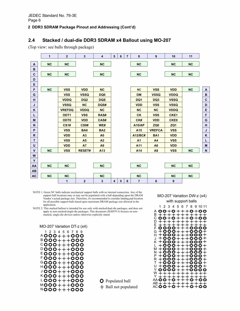
2 DDR3 SDRAM Package Pinout and Addressing (Cont’d)
2.4 Stacked / dual-die DDR3 SDRAM x4 Ballout using MO-207 (Top view: see balls through package)
1 2 3 4 5 6 7 8 9 10 11
A NC NC NC NC NC NCBC NC NC NC NC NC NCDEF NC VSS VDD NC NC VSS VDD NC AG VSS VSSQ DQ0 DM VSSQ VDDQ BH VDDQ DQ2 DQS DQ1 DQ3 VSSQ CJ VSSQ NC DQS# VDD VSS VSSQ DK VREFDQ VDDQ NC NC NC VDDQ EL ODT1 VSS RAS# CK VSS CKE1 FM ODT0 VDD CAS# CK# VDD CKE0 GN CS1# CS0# WE# A10/AP ZQ0 ZQ1 HP VSS BA0 BA2 A15 VREFCA VSS JR VDD A3 A0 A12/BC# BA1 VDD KT VSS A5 A2 A1 A4 VSS LU VDD A7 A9 A11 A6 VDD MV NC VSS RESET# A13 A14 A8 VSS NC NWY
AA NC NC NC NC NC NCABAC NC NC NC NC NC NC
1 2 3 4 5 6 7 8 9
1 2 3 4 8 95 6 7ABCDEFGHJKL
MO-207 Variation DT-z (x4)
NM
1 2 3 4 8 95 6 7ABCDEFGHJKL
MO-207 Variation DW-z (x4)
NM
10 11
PRTUVWY
AAABAC
with support balls
Populated ballBall not populated
NOTE 1: Green NC balls indicate mechanical support balls with no internal connection. Any of the support ball locations may or may not be populated with a ball depending upon the DRAM Vendor’s actual package size. Therefore, it's recommended to consider landing pad location for all possible support balls based upon maximum DRAM package size allowed in the application.
NOTE 2: This stacked ballout is intended for use only with stacked/dual-die packages, and does not apply to non-stacked/single-die packages. This document (JESD79-3) focuses on non-stacked, single-die devices unless otherwise explicitly stated.
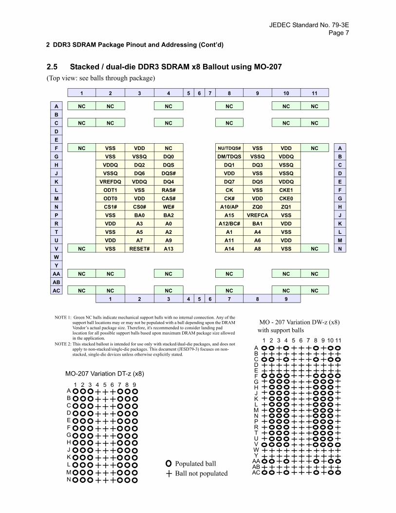
JEDEC Standard No. 79-3EPage 7
2 DDR3 SDRAM Package Pinout and Addressing (Cont’d)
2.5 Stacked / dual-die DDR3 SDRAM x8 Ballout using MO-207(Top view: see balls through package)
1 2 3 4 5 6 7 8 9 10 11
A NC NC NC NC NC NCBC NC NC NC NC NC NCDEF NC VSS VDD NC NU/TDQS# VSS VDD NC AG VSS VSSQ DQ0 DM/TDQS VSSQ VDDQ BH VDDQ DQ2 DQS DQ1 DQ3 VSSQ CJ VSSQ DQ6 DQS# VDD VSS VSSQ DK VREFDQ VDDQ DQ4 DQ7 DQ5 VDDQ EL ODT1 VSS RAS# CK VSS CKE1 FM ODT0 VDD CAS# CK# VDD CKE0 GN CS1# CS0# WE# A10/AP ZQ0 ZQ1 HP VSS BA0 BA2 A15 VREFCA VSS JR VDD A3 A0 A12/BC# BA1 VDD KT VSS A5 A2 A1 A4 VSS LU VDD A7 A9 A11 A6 VDD MV NC VSS RESET# A13 A14 A8 VSS NC NWY
AA NC NC NC NC NC NCABAC NC NC NC NC NC NC
1 2 3 4 5 6 7 8 9
1 2 3 4 8 95 6 7ABCDEFGHJKL
MO-207 Variation DT-z (x8)
NM
1 2 3 4 8 95 6 7ABCDEFGHJKL
NM
10 11
PRTUVWY
AAABAC
Populated ballBall not populated
MO - 207 Variation DW-z (x8) with support balls
NOTE 1: Green NC balls indicate mechanical support balls with no internal connection. Any of the support ball locations may or may not be populated with a ball depending upon the DRAM Vendor’s actual package size. Therefore, it's recommended to consider landing pad location for all possible support balls based upon maximum DRAM package size allowed in the application.
NOTE 2: This stacked ballout is intended for use only with stacked/dual-die packages, and does not apply to non-stacked/single-die packages. This document (JESD79-3) focuses on non-stacked, single-die devices unless otherwise explicitly stated.

JEDEC Standard No. 79-3EPage 8
2 DDR3 SDRAM Package Pinout and Addressing (Cont’d)
2.6 Stacked / dual-die DDR3 SDRAM x16 Ballout using MO-207(Top view: see balls through package)
1 2 3 4 5 6 7 8 9 10 11
A NC NC NC NC NC NCBCD NC VDDQ DQU5 DQU7 DQU4 VDDQ VSS NC AE VSSQ VDD VSS DQSU# DQU6 VSSQ BF VDDQ DQU3 DQU1 DQSU DQU2 VDDQ CG VSSQ VDDQ DMU DQU0 VSSQ VDD DH VSS VSSQ DQL0 DML VSSQ VDDQ EJ VDDQ DQL2 DQSL DQL1 DQL3 VSSQ FK VSSQ DQL6 DQSL# VDD VSS VSSQ GL VREFDQ VDDQ DQL4 DQL7 DQL5 VDDQ HM ODT1 VSS RAS# CK VSS CKE1 JN ODT0 VDD CAS# CK# VDD CKE0 KP CS1# CS0# WE# A10/AP ZQ0 ZQ1 LR VSS BA0 BA2 A15 VREFCA VSS MT VDD A3 A0 A12/BC# BA1 VDD NU VSS A5 A2 A1 A4 VSS PV VDD A7 A9 A11 A6 VDD RW NC VSS RESET# A13 A14 A8 VSS NC TY
AAAB NC NC NC NC NC NC
1 2 3 4 5 6 7 8 9
1 2 3 4 8 95 6 7ABCDEFGHJ
N
10 11
PRTUVWY
AAAB
1 2 3 4 8 95 6 7
ABCDEFGHJKLMNPRT
KLM
Populated ballBall not populated
MO - 207 Variation DU-z (x16)
MO - 207 Variation DY-z(x16) with support balls
NOTE 1: Green NC balls indicate mechanical support balls with no internal connection. Any of the support ball locations may or may not be populated with a ball depending upon the DRAM Vendor’s actual package size. Therefore, it's recommended to consider landing pad location for all possible support balls based upon maximum DRAM package size allowed in the application.
NOTE 2: This stacked ballout is intended for use only with stacked/dual-die packages, and does not apply to non-stacked/single-die packages. This document (JESD79-3) focuses on non-stacked, single-die devices unless otherwise explicitly stated.

JEDEC Standard No. 79-3EPage 9
2 DDR3 SDRAM Package Pinout and Addressing (Cont’d)
2.7 Quad-stacked / Quad-die DDR3 SDRAM x4 Ballout using MO-207(Top view: see balls through package)
1 2 3 4 5 6 7 8 9 10 11
A NC NC NC NC NC NCBC NC NC NC NC NC NCDEF NC VSS VDD NC NC VSS VDD NC AG VSS VSSQ DQ0 DM VSSQ VDDQ BH VDDQ DQ2 DQS DQ1 DQ3 VSSQ CJ VSSQ NC DQS# VDD VSS VSSQ DK VREFDQ VDDQ NC NC NC VDDQ EL ODT1 VSS RAS# CK VSS CKE1 FM ODT0 VDD CAS# CK# VDD CKE0 GN CS1# CS0# WE# A10/AP ZQ0 ZQ1 HP VSS BA0 BA2 A15 VREFCA VSS JR CS2# A3 A0 A12/BC# BA1 ZQ2 KT CS3# A5 A2 A1 A4 ZQ3 LU VDD A7 A9 A11 A6 VDD MV NC VSS RESET# A13 A14 A8 VSS NC NWY
AA NC NC NC NC NC NCABAC NC NC NC NC NC NC
1 2 3 4 5 6 7 8 9
1 2 3 4 8 95 6 7ABCDEFGHJKL
MO-207 Variation DT-z (x4)
NM
1 2 3 4 8 95 6 7ABCDEFGHJKL
MO-207 Variation DW-z (x4)
NM
10 11
PRTUVWY
AAABAC
with support balls
Populated ballBall not populated
NOTE 1: Green NC balls indicate mechanical support balls with no internal connection. Any of the support ball locations may or may not be populated with a ball depending upon the DRAM Vendor’s actual package size. Therefore, it's recommended to consider landing pad location for all possible support balls based upon maximum DRAM package size allowed in the application.
NOTE 2: This stacked ballout is intended for use only with quad-stacked/quad-die packages, and does not apply to non-stacked/single-die packages. This document (JESD79-3) focuses on non-stacked, single-die devices unless otherwise explicitly stated.
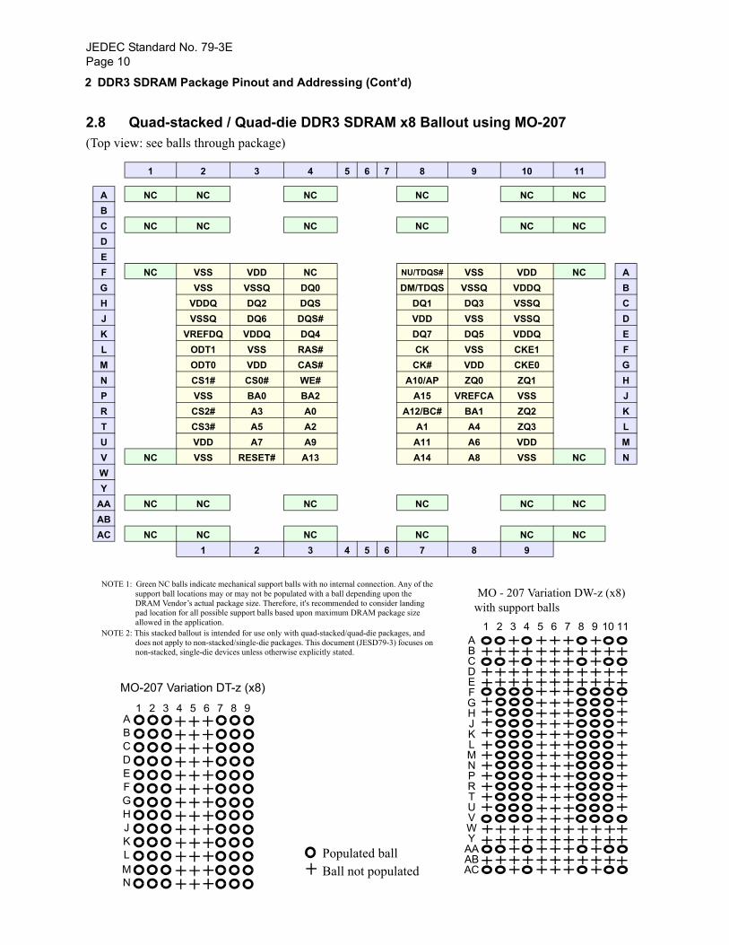
JEDEC Standard No. 79-3EPage 10
2 DDR3 SDRAM Package Pinout and Addressing (Cont’d)
2.8 Quad-stacked / Quad-die DDR3 SDRAM x8 Ballout using MO-207(Top view: see balls through package)
1 2 3 4 5 6 7 8 9 10 11
A NC NC NC NC NC NCBC NC NC NC NC NC NCDEF NC VSS VDD NC NU/TDQS# VSS VDD NC AG VSS VSSQ DQ0 DM/TDQS VSSQ VDDQ BH VDDQ DQ2 DQS DQ1 DQ3 VSSQ CJ VSSQ DQ6 DQS# VDD VSS VSSQ DK VREFDQ VDDQ DQ4 DQ7 DQ5 VDDQ EL ODT1 VSS RAS# CK VSS CKE1 FM ODT0 VDD CAS# CK# VDD CKE0 GN CS1# CS0# WE# A10/AP ZQ0 ZQ1 HP VSS BA0 BA2 A15 VREFCA VSS JR CS2# A3 A0 A12/BC# BA1 ZQ2 KT CS3# A5 A2 A1 A4 ZQ3 LU VDD A7 A9 A11 A6 VDD MV NC VSS RESET# A13 A14 A8 VSS NC NWY
AA NC NC NC NC NC NCABAC NC NC NC NC NC NC
1 2 3 4 5 6 7 8 9
1 2 3 4 8 95 6 7ABCDEFGHJKL
MO-207 Variation DT-z (x8)
NM
1 2 3 4 8 95 6 7ABCDEFGHJKL
NM
10 11
PRTUVWY
AAABAC
Populated ballBall not populated
MO - 207 Variation DW-z (x8) with support balls
NOTE 1: Green NC balls indicate mechanical support balls with no internal connection. Any of the support ball locations may or may not be populated with a ball depending upon the DRAM Vendor’s actual package size. Therefore, it's recommended to consider landing pad location for all possible support balls based upon maximum DRAM package size allowed in the application.
NOTE 2: This stacked ballout is intended for use only with quad-stacked/quad-die packages, and does not apply to non-stacked/single-die packages. This document (JESD79-3) focuses on non-stacked, single-die devices unless otherwise explicitly stated.
JEDEC Standard No. 79-3EPage 11
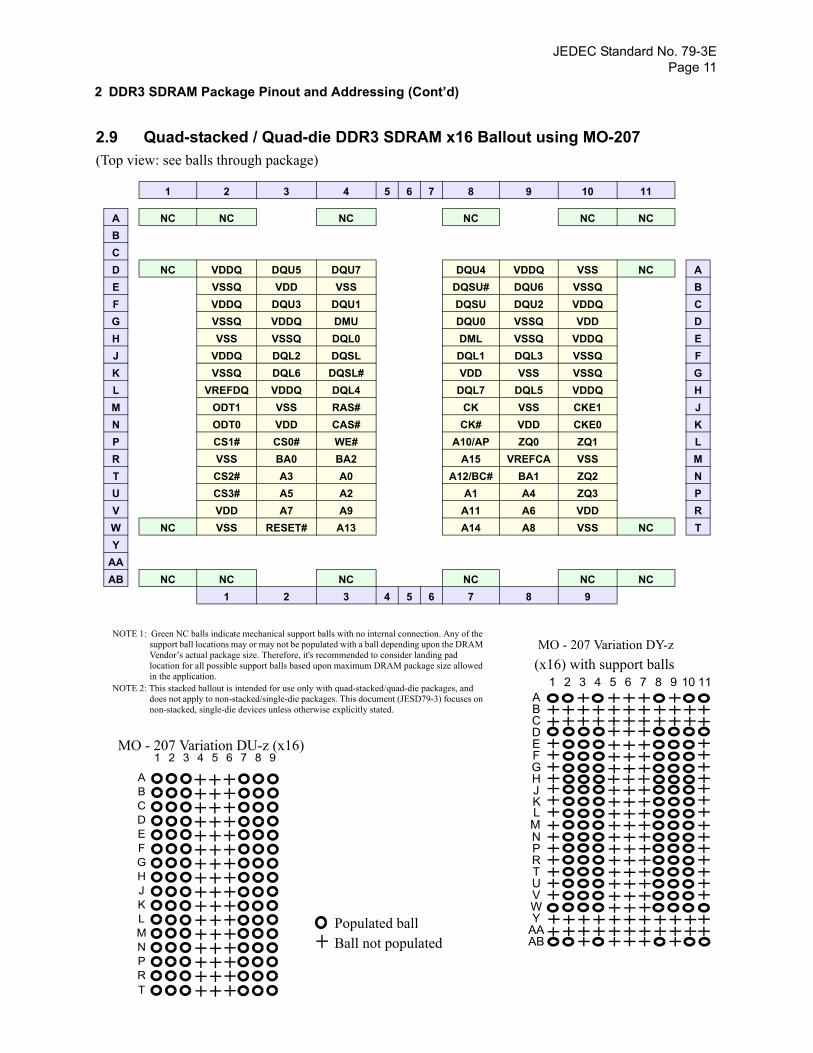
2 DDR3 SDRAM Package Pinout and Addressing (Cont’d)
2.9 Quad-stacked / Quad-die DDR3 SDRAM x16 Ballout using MO-207(Top view: see balls through package)
1 2 3 4 5 6 7 8 9 10 11
A NC NC NC NC NC NCBCD NC VDDQ DQU5 DQU7 DQU4 VDDQ VSS NC AE VSSQ VDD VSS DQSU# DQU6 VSSQ BF VDDQ DQU3 DQU1 DQSU DQU2 VDDQ CG VSSQ VDDQ DMU DQU0 VSSQ VDD DH VSS VSSQ DQL0 DML VSSQ VDDQ EJ VDDQ DQL2 DQSL DQL1 DQL3 VSSQ FK VSSQ DQL6 DQSL# VDD VSS VSSQ GL VREFDQ VDDQ DQL4 DQL7 DQL5 VDDQ HM ODT1 VSS RAS# CK VSS CKE1 JN ODT0 VDD CAS# CK# VDD CKE0 KP CS1# CS0# WE# A10/AP ZQ0 ZQ1 LR VSS BA0 BA2 A15 VREFCA VSS MT CS2# A3 A0 A12/BC# BA1 ZQ2 NU CS3# A5 A2 A1 A4 ZQ3 PV VDD A7 A9 A11 A6 VDD RW NC VSS RESET# A13 A14 A8 VSS NC TY
AAAB NC NC NC NC NC NC
1 2 3 4 5 6 7 8 9
1 2 3 4 8 95 6 7ABCDEFGHJ
N
10 11
PRTUVWY
AAAB
1 2 3 4 8 95 6 7
ABCDEFGHJKLMNPRT
KLM
Populated ballBall not populated
MO - 207 Variation DU-z (x16)
MO - 207 Variation DY-z(x16) with support balls
NOTE 1: Green NC balls indicate mechanical support balls with no internal connection. Any of the support ball locations may or may not be populated with a ball depending upon the DRAM Vendor’s actual package size. Therefore, it's recommended to consider landing pad location for all possible support balls based upon maximum DRAM package size allowed in the application.
NOTE 2: This stacked ballout is intended for use only with quad-stacked/quad-die packages, and does not apply to non-stacked/single-die packages. This document (JESD79-3) focuses on non-stacked, single-die devices unless otherwise explicitly stated.
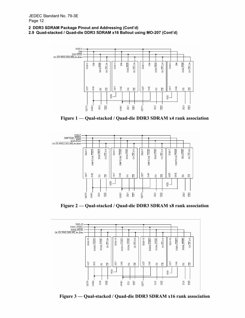
JEDEC Standard No. 79-3EPage 12
Figure 1 — Qual-stacked / Quad-die DDR3 SDRAM x4 rank association
Figure 2 — Qual-stacked / Quad-die DDR3 SDRAM x8 rank association
Figure 3 — Qual-stacked / Quad-die DDR3 SDRAM x16 rank association
2 DDR3 SDRAM Package Pinout and Addressing (Cont’d)2.9 Quad-stacked / Quad-die DDR3 SDRAM x16 Ballout using MO-207 (Cont’d)
JEDEC Standard No. 79-3EPage 13
CK
CK(C
and E is ng
.
C rnal de. QS,
,
R red.
D
is th ister
e ssed
ead//AP
code
and ). If
hop
ail-30V
ered nds
robe
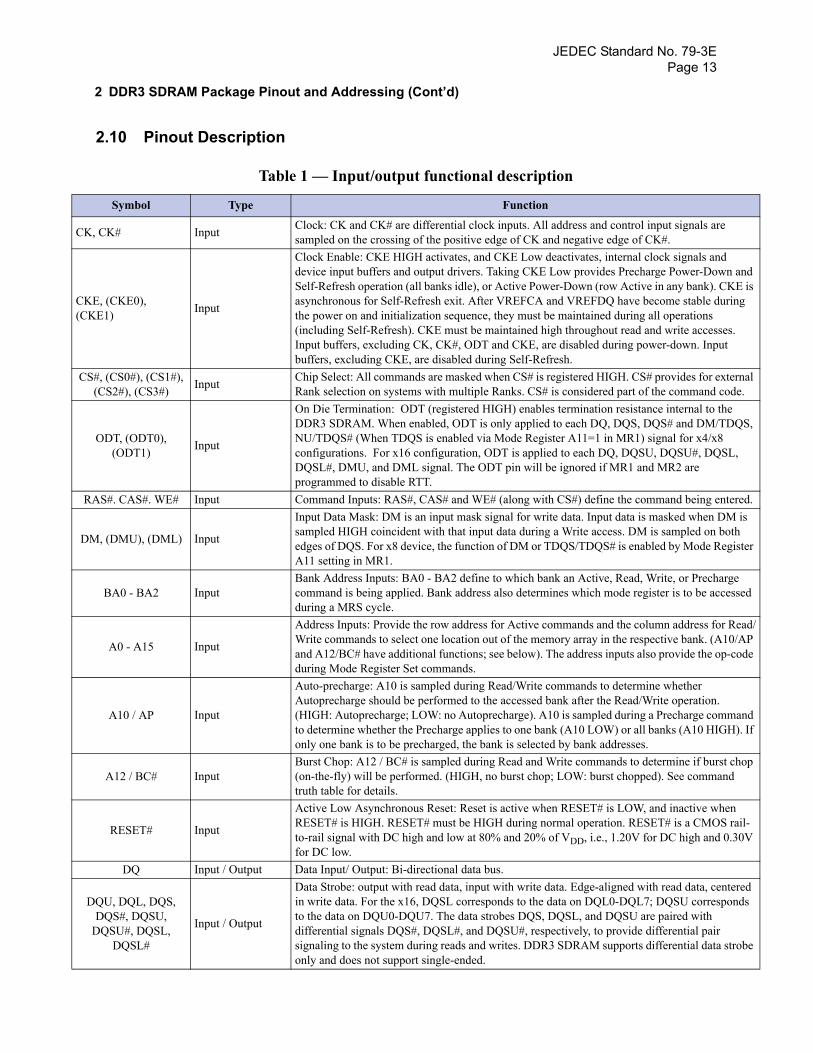
2.10 Pinout Description
Table 1 — Input/output functional description
Symbol Type Function
, CK# Input Clock: CK and CK# are differential clock inputs. All address and control input signals are sampled on the crossing of the positive edge of CK and negative edge of CK#.
E, (CKE0), KE1) Input
Clock Enable: CKE HIGH activates, and CKE Low deactivates, internal clock signals and device input buffers and output drivers. Taking CKE Low provides Precharge Power-DownSelf-Refresh operation (all banks idle), or Active Power-Down (row Active in any bank). CKasynchronous for Self-Refresh exit. After VREFCA and VREFDQ have become stable durithe power on and initialization sequence, they must be maintained during all operations (including Self-Refresh). CKE must be maintained high throughout read and write accessesInput buffers, excluding CK, CK#, ODT and CKE, are disabled during power-down. Input buffers, excluding CKE, are disabled during Self-Refresh.
S#, (CS0#), (CS1#), (CS2#), (CS3#) Input Chip Select: All commands are masked when CS# is registered HIGH. CS# provides for exte
Rank selection on systems with multiple Ranks. CS# is considered part of the command co
ODT, (ODT0), (ODT1) Input
On Die Termination: ODT (registered HIGH) enables termination resistance internal to theDDR3 SDRAM. When enabled, ODT is only applied to each DQ, DQS, DQS# and DM/TDNU/TDQS# (When TDQS is enabled via Mode Register A11=1 in MR1) signal for x4/x8 configurations. For x16 configuration, ODT is applied to each DQ, DQSU, DQSU#, DQSLDQSL#, DMU, and DML signal. The ODT pin will be ignored if MR1 and MR2 are programmed to disable RTT.
AS#. CAS#. WE# Input Command Inputs: RAS#, CAS# and WE# (along with CS#) define the command being ente
M, (DMU), (DML) Input
Input Data Mask: DM is an input mask signal for write data. Input data is masked when DMsampled HIGH coincident with that input data during a Write access. DM is sampled on boedges of DQS. For x8 device, the function of DM or TDQS/TDQS# is enabled by Mode RegA11 setting in MR1.
BA0 - BA2 InputBank Address Inputs: BA0 - BA2 define to which bank an Active, Read, Write, or Prechargcommand is being applied. Bank address also determines which mode register is to be acceduring a MRS cycle.
A0 - A15 Input
Address Inputs: Provide the row address for Active commands and the column address for RWrite commands to select one location out of the memory array in the respective bank. (A10and A12/BC# have additional functions; see below). The address inputs also provide the op-during Mode Register Set commands.
A10 / AP Input
Auto-precharge: A10 is sampled during Read/Write commands to determine whether Autoprecharge should be performed to the accessed bank after the Read/Write operation. (HIGH: Autoprecharge; LOW: no Autoprecharge). A10 is sampled during a Precharge commto determine whether the Precharge applies to one bank (A10 LOW) or all banks (A10 HIGHonly one bank is to be precharged, the bank is selected by bank addresses.
A12 / BC# InputBurst Chop: A12 / BC# is sampled during Read and Write commands to determine if burst c(on-the-fly) will be performed. (HIGH, no burst chop; LOW: burst chopped). See commandtruth table for details.
RESET# Input
Active Low Asynchronous Reset: Reset is active when RESET# is LOW, and inactive whenRESET# is HIGH. RESET# must be HIGH during normal operation. RESET# is a CMOS rto-rail signal with DC high and low at 80% and 20% of VDD, i.e., 1.20V for DC high and 0.for DC low.
DQ Input / Output Data Input/ Output: Bi-directional data bus.
DQU, DQL, DQS, DQS#, DQSU,
DQSU#, DQSL, DQSL#
Input / Output
Data Strobe: output with read data, input with write data. Edge-aligned with read data, centin write data. For the x16, DQSL corresponds to the data on DQL0-DQL7; DQSU correspoto the data on DQU0-DQU7. The data strobes DQS, DQSL, and DQSU are paired with differential signals DQS#, DQSL#, and DQSU#, respectively, to provide differential pair signaling to the system during reads and writes. DDR3 SDRAM supports differential data stonly and does not support single-ended.
2 DDR3 SDRAM Package Pinout and Addressing (Cont’d)
JEDEC Standard No. 79-3EPage 14
via tion in Ms
up-
2 DDR3 SDRAM Package Pinout and Addressing (Cont’d)2.10 Pinout Description (Cont’d)
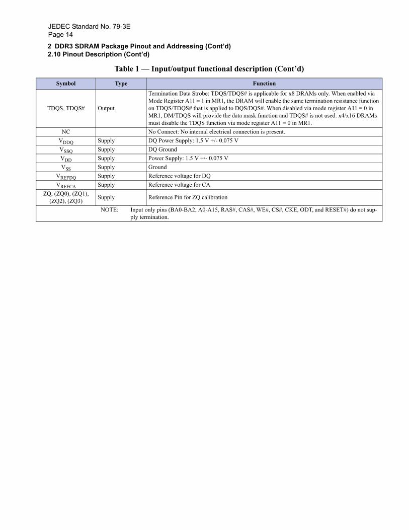
TDQS, TDQS# Output
Termination Data Strobe: TDQS/TDQS# is applicable for x8 DRAMs only. When enabled Mode Register A11 = 1 in MR1, the DRAM will enable the same termination resistance funcon TDQS/TDQS# that is applied to DQS/DQS#. When disabled via mode register A11 = 0 MR1, DM/TDQS will provide the data mask function and TDQS# is not used. x4/x16 DRAmust disable the TDQS function via mode register A11 = 0 in MR1.
NC No Connect: No internal electrical connection is present.VDDQ Supply DQ Power Supply: 1.5 V +/- 0.075 VVSSQ Supply DQ GroundVDD Supply Power Supply: 1.5 V +/- 0.075 VVSS Supply Ground
VREFDQ Supply Reference voltage for DQVREFCA Supply Reference voltage for CA
ZQ, (ZQ0), (ZQ1), (ZQ2), (ZQ3) Supply Reference Pin for ZQ calibration
NOTE: Input only pins (BA0-BA2, A0-A15, RAS#, CAS#, WE#, CS#, CKE, ODT, and RESET#) do not sply termination.
Table 1 — Input/output functional description (Cont’d)
Symbol Type Function

JEDEC Standard No. 79-3EPage 15
2 DDR3 SDRAM Package Pinout and Addressing (Cont’d)
2.11 DDR3 SDRAM Addressing2.11.1 512Mb
2.11.2 1Gb
2.11.3 2Gb
2.11.4 4Gb
Configuration 128Mb x 4 64Mb x 8 32Mb x 16
# of Banks 8 8 8
Bank Address BA0 - BA2 BA0 - BA2 BA0 - BA2
Auto precharge A10/AP A10/AP A10/AP
BC switch on the fly A12/BC# A12/BC# A12/BC#
Row Address A0 - A12 A0 - A12 A0 - A11
Column Address A0 - A9,A11 A0 - A9 A0 - A9
Page size 1 1 KB 1 KB 2 KB
Configuration 256Mb x 4 128Mb x 8 64Mb x 16
# of Banks 8 8 8
Bank Address BA0 - BA2 BA0 - BA2 BA0 - BA2
Auto precharge A10/AP A10/AP A10/AP
BC switch on the fly A12/BC# A12/BC# A12/BC#
Row Address A0 - A13 A0 - A13 A0 - A12
Column Address A0 - A9,A11 A0 - A9 A0 - A9
Page size 1 1 KB 1 KB 2 KB
Configuration 512Mb x 4 256Mb x 8 128Mb x 16
# of Banks 8 8 8
Bank Address BA0 - BA2 BA0 - BA2 BA0 - BA2
Auto precharge A10/AP A10/AP A10/AP
BC switch on the fly A12/BC# A12/BC# A12/BC#
Row Address A0 - A14 A0 - A14 A0 - A13
Column Address A0 - A9,A11 A0 - A9 A0 - A9
Page size 1 1 KB 1 KB 2 KB
Configuration 1Gb x 4 512Mb x 8 256Mb x 16
# of Banks 8 8 8
Bank Address BA0 - BA2 BA0 - BA2 BA0 - BA2
Auto precharge A10/AP A10/AP A10/AP
BC switch on the fly A12/BC# A12/BC# A12/BC#
Row Address A0 - A15 A0 - A15 A0 - A14
Column Address A0 - A9,A11 A0 - A9 A0 - A9
Page size 1 1 KB 1 KB 2 KB
JEDEC Standard No. 79-3EPage 16
2 DDR3 SDRAM Package Pinout and Addressing (Cont’d)2.11 DDR3 SDRAM Addressing (Cont’d)
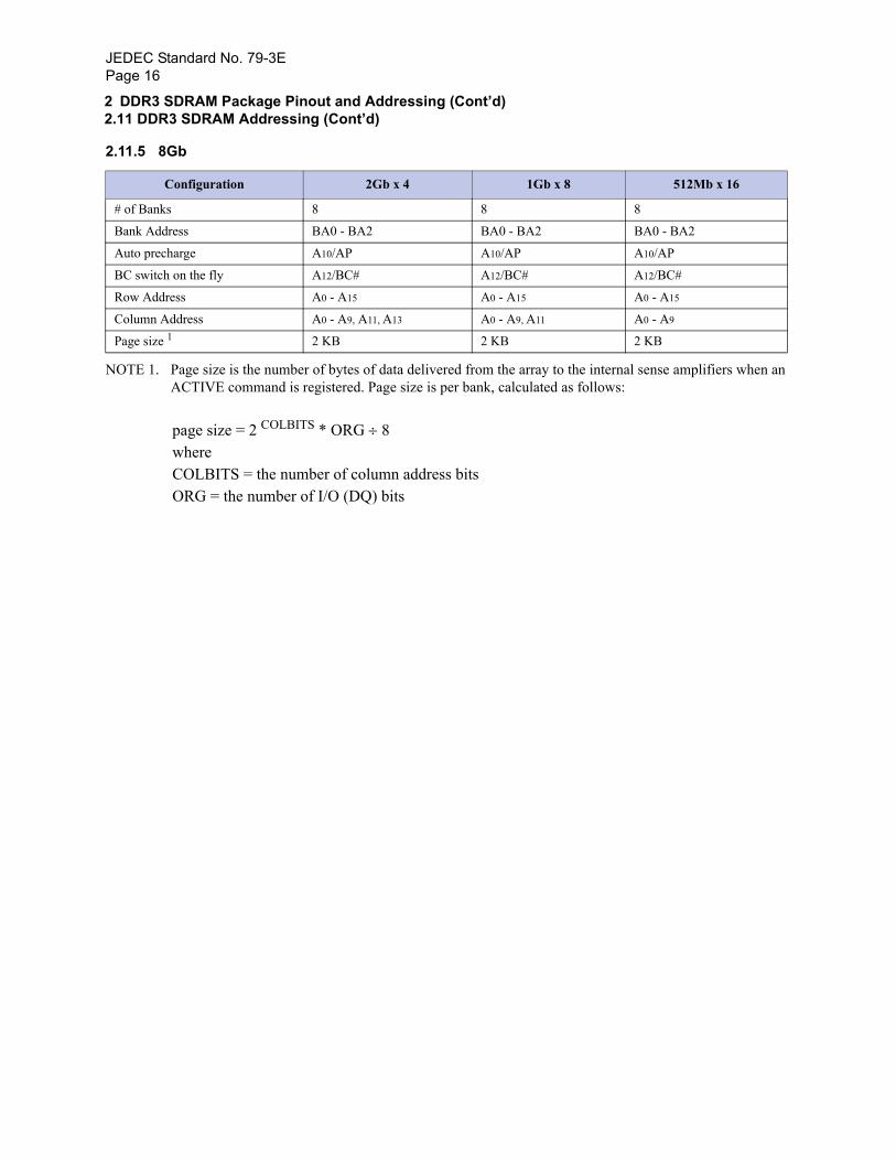
2.11.5 8Gb
NOTE 1. Page size is the number of bytes of data delivered from the array to the internal sense amplifiers when an ACTIVE command is registered. Page size is per bank, calculated as follows:
page size = 2 COLBITS * ORG ÷ 8where COLBITS = the number of column address bitsORG = the number of I/O (DQ) bits
Configuration 2Gb x 4 1Gb x 8 512Mb x 16
# of Banks 8 8 8
Bank Address BA0 - BA2 BA0 - BA2 BA0 - BA2
Auto precharge A10/AP A10/AP A10/AP
BC switch on the fly A12/BC# A12/BC# A12/BC#
Row Address A0 - A15 A0 - A15 A0 - A15
Column Address A0 - A9, A11, A13 A0 - A9, A11 A0 - A9
Page size 1 2 KB 2 KB 2 KB
JEDEC Standard No. 79-3EPage 17
Ab
r
3 Functional Description
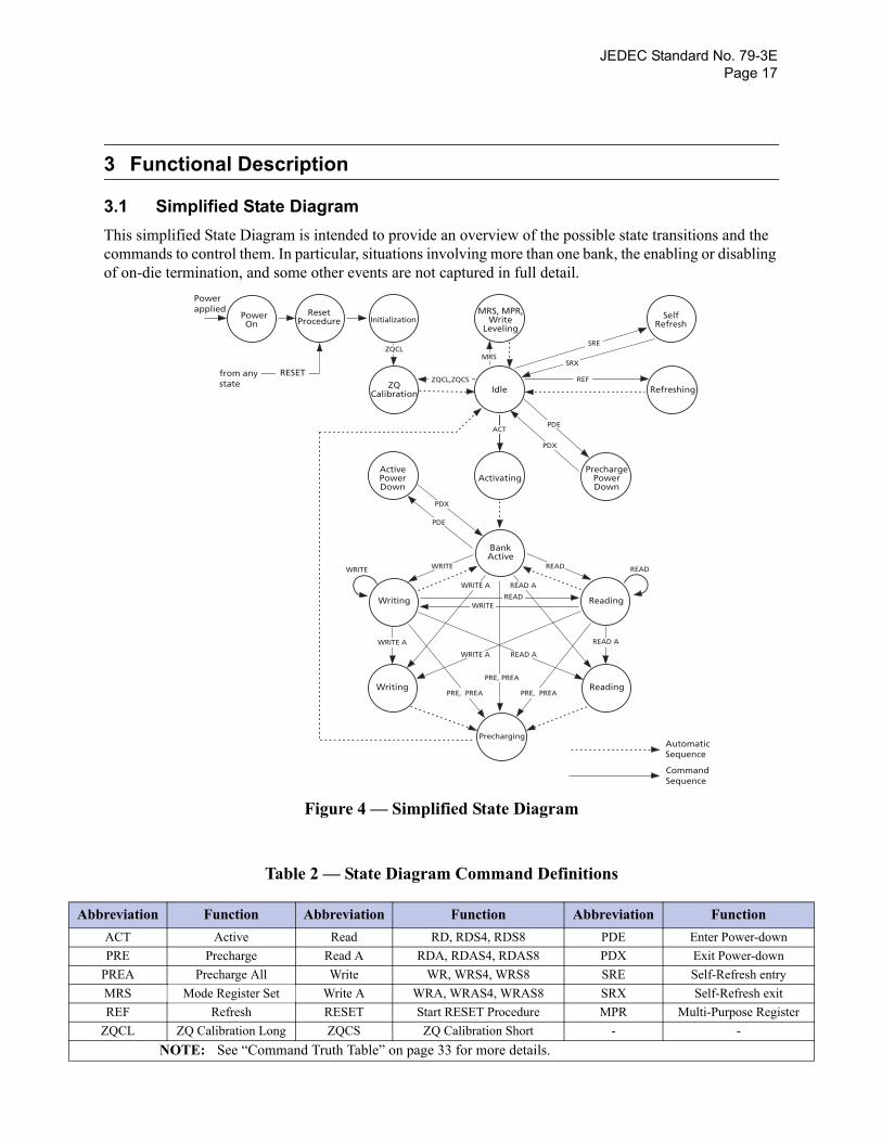
3.1 Simplified State DiagramThis simplified State Diagram is intended to provide an overview of the possible state transitions and the commands to control them. In particular, situations involving more than one bank, the enabling or disabling of on-die termination, and some other events are not captured in full detail.
Figure 4 — Simplified State Diagram
Table 2 — State Diagram Command Definitions
breviation Function Abbreviation Function Abbreviation FunctionACT Active Read RD, RDS4, RDS8 PDE Enter Power-downPRE Precharge Read A RDA, RDAS4, RDAS8 PDX Exit Power-down
PREA Precharge All Write WR, WRS4, WRS8 SRE Self-Refresh entryMRS Mode Register Set Write A WRA, WRAS4, WRAS8 SRX Self-Refresh exitREF Refresh RESET Start RESET Procedure MPR Multi-Purpose Registe
ZQCL ZQ Calibration Long ZQCS ZQ Calibration Short - -NOTE: See “Command Truth Table” on page 33 for more details.
BankActive
ReadingWriting
Activating
Refreshing
SelfRefresh
Idle
ActivePowerDown
ZQCalibration
from anystate
Powerapplied Reset
Procedure Power
On InitializationMRS, MPR,
WriteLeveling
PrechargePowerDown
Writing Reading
AutomaticSequence
CommandSequence
Precharging
READ
READ READ
READ A
READ A
READ A
PRE, PREA
PRE, PREA PRE, PREA
WRITE
WRITEWRITE
WRITE A
WRITE A
WRITE A
PDE
PDE
PDX
PDX
SRX
SRE
REF
MRS
ACT
RESET
ZQCL
ZQCL,ZQCS
JEDEC Standard No. 79-3EPage 18
3 Functional Description (Cont’d)
3.2 Basic FunctionalityThe DDR3 SDRAM is a high-speed dynamic random-access memory internally configured as an eight-bank DRAM. The DDR3 SDRAM uses a 8n prefetch architecture to achieve high-speed operation. The 8n prefetch architecture is combined with an interface designed to transfer two data words per clock cycle at the I/O pins. A single read or write operation for the DDR3 SDRAM consists of a single 8n-bit wide, four clock data transfer at the internal DRAM core and two corresponding n-bit wide, one-half clock cycle data transfers at the I/O pins.
Read and write operation to the DDR3 SDRAM are burst oriented, start at a selected location, and continue for a burst length of eight or a ‘chopped’ burst of four in a programmed sequence. Operation begins with the registration of an Active command, which is then followed by a Read or Write command. The address bits registered coincident with the Active command are used to select the bank and row to be activated (BA0-BA2 select the bank; A0-A15 select the row; refer to “DDR3 SDRAM Addressing” on page 15 for specific requirements). The address bits registered coincident with the Read or Write command are used to select the starting column location for the burst operation, determine if the auto precharge command is to be issued (via A10), and select BC4 or BL8 mode ‘on the fly’ (via A12) if enabled in the mode register.
Prior to normal operation, the DDR3 SDRAM must be powered up and initialized in a predefined manner. The following sections provide detailed information covering device reset and initialization, register defi-nition, command descriptions, and device operation.
JEDEC Standard No. 79-3EPage 19
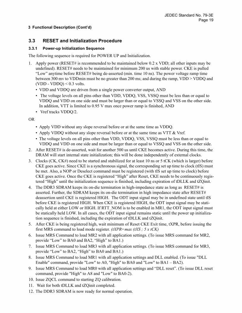
3 Functional Description (Cont’d)
3.3 RESET and Initialization Procedure3.3.1 Power-up Initialization Sequence
The following sequence is required for POWER UP and Initialization.
1. Apply power (RESET# is recommended to be maintained below 0.2 x VDD; all other inputs may be undefined). RESET# needs to be maintained for minimum 200 us with stable power. CKE is pulled “Low” anytime before RESET# being de-asserted (min. time 10 ns). The power voltage ramp time between 300 mv to VDDmin must be no greater than 200 ms; and during the ramp, VDD > VDDQ and (VDD - VDDQ) < 0.3 volts.• VDD and VDDQ are driven from a single power converter output, AND• The voltage levels on all pins other than VDD, VDDQ, VSS, VSSQ must be less than or equal to
VDDQ and VDD on one side and must be larger than or equal to VSSQ and VSS on the other side. In addition, VTT is limited to 0.95 V max once power ramp is finished, AND
• Vref tracks VDDQ/2.
OR
• Apply VDD without any slope reversal before or at the same time as VDDQ.• Apply VDDQ without any slope reversal before or at the same time as VTT & Vref.
• The voltage levels on all pins other than VDD, VDDQ, VSS, VSSQ must be less than or equal to VDDQ and VDD on one side and must be larger than or equal to VSSQ and VSS on the other side.
2. After RESET# is de-asserted, wait for another 500 us until CKE becomes active. During this time, the DRAM will start internal state initialization; this will be done independently of external clocks.
3. Clocks (CK, CK#) need to be started and stabilized for at least 10 ns or 5 tCK (which is larger) before CKE goes active. Since CKE is a synchronous signal, the corresponding set up time to clock (tIS) must be met. Also, a NOP or Deselect command must be registered (with tIS set up time to clock) before CKE goes active. Once the CKE is registered “High” after Reset, CKE needs to be continuously regis-tered “High” until the initialization sequence is finished, including expiration of tDLLK and tZQinit.
4. The DDR3 SDRAM keeps its on-die termination in high-impedance state as long as RESET# is asserted. Further, the SDRAM keeps its on-die termination in high impedance state after RESET# deassertion until CKE is registered HIGH. The ODT input signal may be in undefined state until tIS before CKE is registered HIGH. When CKE is registered HIGH, the ODT input signal may be stati-cally held at either LOW or HIGH. If RTT_NOM is to be enabled in MR1, the ODT input signal must be statically held LOW. In all cases, the ODT input signal remains static until the power up initializa-tion sequence is finished, including the expiration of tDLLK and tZQinit.
5. After CKE is being registered high, wait minimum of Reset CKE Exit time, tXPR, before issuing the first MRS command to load mode register. (tXPR=max (tXS ; 5 x tCK)
6. Issue MRS Command to load MR2 with all application settings. (To issue MRS command for MR2, provide “Low” to BA0 and BA2, “High” to BA1.)
7. Issue MRS Command to load MR3 with all application settings. (To issue MRS command for MR3, provide “Low” to BA2, “High” to BA0 and BA1.)
8. Issue MRS Command to load MR1 with all application settings and DLL enabled. (To issue "DLL Enable" command, provide "Low" to A0, "High" to BA0 and "Low" to BA1 – BA2).
9. Issue MRS Command to load MR0 with all application settings and “DLL reset”. (To issue DLL reset command, provide "High" to A8 and "Low" to BA0-2).
10. Issue ZQCL command to starting ZQ calibration.11. Wait for both tDLLK and tZQinit completed.12. The DDR3 SDRAM is now ready for normal operation.

JEDEC Standard No. 79-3EPage 20
C
COMM
R
VDD,
3.3 RESET and Initialization Procedure (Cont’d)3.3.1 Power-up Initialization Sequence (Cont’d)
Figure 5 — Reset and Initialization Sequence at Power-on Ramping
()()
()()
CKE
RTT
BA
T = 200µs
()()
()()
K, CK#
AND 1) 1)
()()
()()
TdTc Tg
DON’T CARE
()()
()()
()()
tIS
ODT
()()
()()
Th
tMRD tMOD
()()
()()
()()
()()
MRSMRS
()()
()()
()()
()()
()()
()()
()()
()()
()()
()()
()()
()()
VALID
VALID
tMRD tMRD
()()
()()
()()
()()
MRS
MR0MR1MR3
MRS
MR2
()()
()()
()()
()()
()()
()()
Ti Tj Tk
()()
()()
ESET#
()()
()()
()()
()()
()()
()()
()()
()()
()()
T = 500µs
()()
()()
()()
()()
()()
()()
()()
VALID
TeTa Tb Tf
()()
()()
ZQCL
()()
()()
()()
()()
()()
()()
()()
()()
()()
()()
tIS
Static LOW in case RTT_Nom is enabled at time Tg, otherwise static HIGH or LOW
()()
()()
()()
()()
tIS tIS
tXPR
()()
()()
()()
()()
()()
()()
()()
()()
TIME BREAK
VALID
()()
()()
()()
()()
()()
Tmin = 10ns
VDDQ()()
()()
()()
()()
()()
()()
()()
()()
()()
()()
()()
()()
()()
NOTE 1. From time point “Td” until “Tk” NOP or DES commands must be applied between MRS and ZQCL commands.
tDLLK
()()
()()
()()
()()
tZQinit
()()
()()
()()
()()
()()
()()
()()
()()
()()
()()
()()
()()
()()
()()
()()
()()
()()
()()
tCKSRX
()()
()()
()()
()()
()()
()()

JEDEC Standard No. 79-3EPage 21
CK
COMM
R
VDD,
N
3 Functional Description (Cont’d)3.3 RESET and Initialization Procedure (Cont’d)
3.3.2 Reset Initialization with Stable Power
The following sequence is required for RESET at no power interruption initialization.
1. Asserted RESET below 0.2 * VDD anytime when reset is needed (all other inputs may be undefined). RESET needs to be maintained for minimum 100 ns. CKE is pulled “LOW” before RESET being de-asserted (min. time 10 ns).
2. Follow Power-up Initialization Sequence steps 2 to 11.3. The Reset sequence is now completed; DDR3 SDRAM is ready for normal operation.
Figure 6 — Reset Procedure at Power Stable Condition
()()
()()
CKE
RTT
BA
T = 100 ns
()()
()()
, CK#
AND 1) 1)
()()
()()
TdTc Tg
DON’T CARE
()()
()()
()()
tIS
ODT
()()
()()
Th
tMRD tMOD
()()
()()
()()
()()
MRSMRS
()()
()()
()()
()()
()()
()()
()()
()()
()()
()()
()()
()()
VALID
VALID
tMRD tMRD
()()
()()
()()
()()
MRS
MR0MR1MR3
MRS
MR2
()()
()()
()()
()()
()()
()()
Ti Tj Tk
()()
()()
ESET#
()()
()()
()()
()()
()()
()()
()()
()()
()()
T = 500µs
()()
()()
()()
()()
()()
VALID
TeTa Tb Tf
()()
()()
ZQCL
()()
()()
()()
()()
()()
()()
()()
()()
()()
()()
tIS
Static LOW in case RTT_Nom is enabled at time Tg, otherwise static HIGH or LOW
()()
()()
()()
()()
tIS tIS
tXPR
()()
()()
()()
()()
()()
()()
()()
()()
TIME BREAK
VALID
()()
()()
()()
()()
()()
Tmin = 10ns
tCKSRX
VDDQ()()
()()
()()
()()
()()
()()
()()
()()
()()
()()
()()
()()
()()
OTE 1. From time point “Td” until “Tk” NOP or DES commands must be applied between MRS and ZQCL commands.
tDLLK
()()
()()
()()
()()
tZQinit
()()
()()
()()
()()
()()
()()
()()
()()
()()
()()
()()
()()
()()
()()
()()
()()
()()
()()
()()
()()
()()
()()
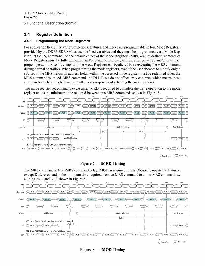
JEDEC Standard No. 79-3EPage 22
are
Com
Se
Ad
Comm
O
Sett
O
Add
re
3 Functional Description (Cont’d)
3.4 Register Definition3.4.1 Programming the Mode Registers
For application flexibility, various functions, features, and modes are programmable in four Mode Registers, provided by the DDR3 SDRAM, as user defined variables and they must be programmed via a Mode Reg-ister Set (MRS) command. As the default values of the Mode Registers (MR#) are not defined, contents of Mode Registers must be fully initialized and/or re-initialized, i.e., written, after power up and/or reset for proper operation. Also the contents of the Mode Registers can be altered by re-executing the MRS command during normal operation. When programming the mode registers, even if the user chooses to modify only a sub-set of the MRS fields, all address fields within the accessed mode register must be redefined when the MRS command is issued. MRS command and DLL Reset do not affect array contents, which means these commands can be executed any time after power-up without affecting the array contents.
The mode register set command cycle time, tMRD is required to complete the write operation to the mode register and is the minimum time required between two MRS commands shown in Figure 7 .
Figure 7 — tMRD TimingThe MRS command to Non-MRS command delay, tMOD, is required for the DRAM to update the features, except DLL reset, and is the minimum time required from an MRS command to a non-MRS command ex-cluding NOP and DES shown in Figure 8.
Figure 8 — tMOD Timing
T0 T1 T2 Ta0 Ta1 Tb0 Tb1 Tb2 Tc0 Tc1 Tc2
Don’t C
VALIDVALID VALID MRS NOP/DES NOP/DES MRS NOP/DES NOP/DES VALID VALID
CK
CK#
mand
VALIDVALID VALID VALID VALIDVALIDVALIDVALIDVALIDVALIDVALIDODT
ttings
CKE
Old Settings Updating Settings New Settings
VALID VALID VALIDODT
dress VALID VALID VALID VALID VALID VALID VALID VALID VALID VALID VALID
tMRD tMOD
()()
()()
Time Break
RTT_Nom ENABLED prior and/or after MRS command
RTT_Nom DISABLED prior and after MRS command
ODTLoff + 1
T0 T1 T2 Ta0 Ta1 Ta2 Ta3 Ta4 Tb0 Tb1 Tb2
VALIDVALID VALID MRS NOP/DES NOP/DES NOP/DES NOP/DESNOP/DES VALIDVALID
CK
CK#
and
VALIDVALID VALID VALID VALIDVALIDVALIDVALIDVALIDVALIDVALIDDT
ings
CKE
Old Settings Updating Settings New Settings
VALID VALID VALIDDT
ress VALID VALID VALID VALID VALID VALID VALID VALID VALID VALID VALID
tMOD
Don’t Ca()()
()()
Time Break
RTT_Nom ENABLED prior and/or after MRS command
RTT_Nom DISABLED prior and after MRS command
ODTLoff + 1
JEDEC Standard No. 79-3EPage 23
3.4 Register Definition (Cont’d)3.4.1 Programming the Mode Registers (Cont’d)
The mode register contents can be changed using the same command and timing requirements during nor-mal operation as long as the DRAM is in idle state, i.e., all banks are in the precharged state with tRP satis-fied, all data bursts are completed and CKE is high prior to writing into the mode register. If the RTT_NOM Feature is enabled in the Mode Register prior and/or after an MRS Command, the ODT Signal must contin-uously be registered LOW ensuring RTT is in an off State prior to the MRS command. The ODT Signal may be registered high after tMOD has expired. If the RTT_NOM Feature is disabled in the Mode Register prior and after an MRS command, the ODT Signal can be registered either LOW or HIGH before, during and after the MRS command. The mode registers are divided into various fields depending on the functionality and/or modes.
3.4.2 Mode Register MR0
The mode register MR0 stores the data for controlling various operating modes of DDR3 SDRAM. It con-trols burst length, read burst type, CAS latency, test mode, DLL reset, WR and DLL control for precharge Power-Down, which include various vendor specific options to make DDR3 SDRAM useful for various ap-plications. The mode register is written by asserting low on CS#, RAS#, CAS#, WE#, BA0, BA1, and BA2,

JEDEC Standard No. 79-3EPage 24
*1:
*2: xt an
*3:
*4:
B
3.4 Register Definition (Cont’d)3.4.2 Mode Register MR0 (Cont’d)
while controlling the states of address pins according to Figure 9.
Figure 9 — MR0 Definition
Address Field
A7 mode
0 Normal
1 Test
A3 Read Burst Type
0 Nibble Sequential
1 Interleave
A8 DLL Reset
0 No
1 Yes
Mode Register 0
BA1 BA0 A11 A10 A9 A8 A7 A6 A5 A4 A3 A2 A1 A0
0 TM CAS Latency RBTDLL 0*1 WR
Write recovery for autoprecharge
A11 A10 A9 WR(cycles)
0 0 0 16*2
0 0 1 5*2
0 1 0 6*2
0 1 1 7*2
1 0 0 8*2
1 0 1 10*2
1 1 0 12*2
1 1 1 14*2
A15 ~ A13
0 BL
A1 A0 BL
0 0 8 (Fixed)
0 1 BC4 or 8 (on the fly)
1 0 BC4 (Fixed)
1 1 Reserved
BA2 and A13~A15 are RFU and must be programmed to 0 during MRS.
WR (write recovery for autoprecharge)min in clock cycles is calculated by dividing tWR(in ns) by tCK(in ns) and rounding up to the neinteger: WRmin[cycles] = Roundup(tWR[ns] / tCK[ns]). The WR value in the mode register must be programmed to be equal or larger thWRmin. The programmed WR value is used with tRP to determine tDAL.
The table only shows the encodings for a given Cas Latency. For actual supported Cas Latency, please refer to speedbin tables for eachfrequency
The table only shows the encodings for Write Recovery. For actual Write recovery timing, please refer to AC timingtable.
BA2
0*1
A1 BA0 MR Select
0 0 MR0
0 1 MR1
1 0 MR2
1 1 MR3
A12
PPD
A12 DLL Control for Precharge PD
0 Slow exit (DLL off)
1 Fast exit (DLL on)A6 A5 A4 A2 CAS Latency
0 0 0 0 Reserved
0 0 1 0 5
0 1 0 0 6
0 1 1 0 7
1 0 0 0 8
1 0 1 0 9
1 1 0 0 10
1 1 1 0 11 (Optional for DDR3-1600)
0 0 0 1 12
0 0 1 1 13
0 1 0 1 14
0 1 1 1 Reserved for 15
1 0 0 1 Reserved for 16
1 0 1 1 Reserved
1 1 0 1 Reserved
1 1 1 1 Reserved
CL
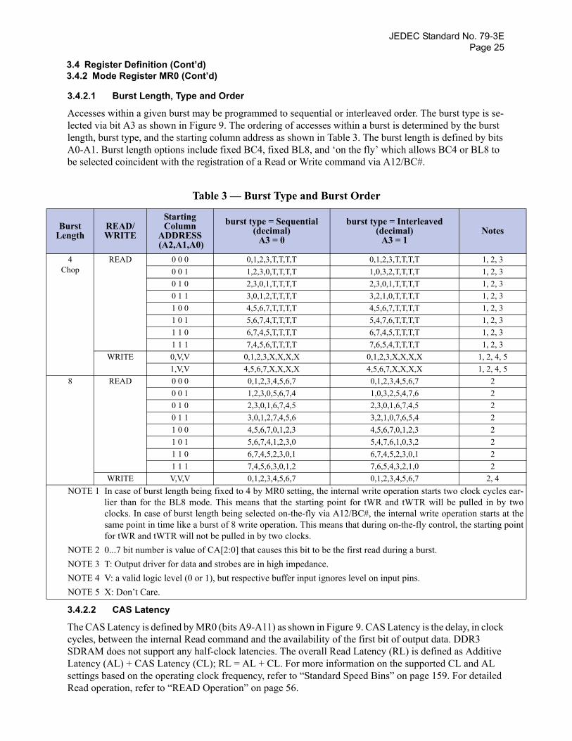
JEDEC Standard No. 79-3EPage 25
L
r-o
hent
3.4 Register Definition (Cont’d)3.4.2 Mode Register MR0 (Cont’d)
3.4.2.1 Burst Length, Type and Order
Accesses within a given burst may be programmed to sequential or interleaved order. The burst type is se-lected via bit A3 as shown in Figure 9. The ordering of accesses within a burst is determined by the burst length, burst type, and the starting column address as shown in Table 3. The burst length is defined by bits A0-A1. Burst length options include fixed BC4, fixed BL8, and ‘on the fly’ which allows BC4 or BL8 to be selected coincident with the registration of a Read or Write command via A12/BC#.
3.4.2.2 CAS Latency
The CAS Latency is defined by MR0 (bits A9-A11) as shown in Figure 9. CAS Latency is the delay, in clock cycles, between the internal Read command and the availability of the first bit of output data. DDR3 SDRAM does not support any half-clock latencies. The overall Read Latency (RL) is defined as Additive Latency (AL) + CAS Latency (CL); RL = AL + CL. For more information on the supported CL and AL settings based on the operating clock frequency, refer to “Standard Speed Bins” on page 159. For detailed Read operation, refer to “READ Operation” on page 56.
Table 3 — Burst Type and Burst Order
Burst ength
READ/WRITE
Starting Column
ADDRESS (A2,A1,A0)
burst type = Sequential (decimal)
A3 = 0
burst type = Interleaved (decimal)
A3 = 1Notes
4Chop
READ 0 0 0 0,1,2,3,T,T,T,T 0,1,2,3,T,T,T,T 1, 2, 30 0 1 1,2,3,0,T,T,T,T 1,0,3,2,T,T,T,T 1, 2, 30 1 0 2,3,0,1,T,T,T,T 2,3,0,1,T,T,T,T 1, 2, 30 1 1 3,0,1,2,T,T,T,T 3,2,1,0,T,T,T,T 1, 2, 31 0 0 4,5,6,7,T,T,T,T 4,5,6,7,T,T,T,T 1, 2, 31 0 1 5,6,7,4,T,T,T,T 5,4,7,6,T,T,T,T 1, 2, 31 1 0 6,7,4,5,T,T,T,T 6,7,4,5,T,T,T,T 1, 2, 31 1 1 7,4,5,6,T,T,T,T 7,6,5,4,T,T,T,T 1, 2, 3
WRITE 0,V,V 0,1,2,3,X,X,X,X 0,1,2,3,X,X,X,X 1, 2, 4, 51,V,V 4,5,6,7,X,X,X,X 4,5,6,7,X,X,X,X 1, 2, 4, 5
8 READ 0 0 0 0,1,2,3,4,5,6,7 0,1,2,3,4,5,6,7 20 0 1 1,2,3,0,5,6,7,4 1,0,3,2,5,4,7,6 20 1 0 2,3,0,1,6,7,4,5 2,3,0,1,6,7,4,5 20 1 1 3,0,1,2,7,4,5,6 3,2,1,0,7,6,5,4 21 0 0 4,5,6,7,0,1,2,3 4,5,6,7,0,1,2,3 21 0 1 5,6,7,4,1,2,3,0 5,4,7,6,1,0,3,2 21 1 0 6,7,4,5,2,3,0,1 6,7,4,5,2,3,0,1 21 1 1 7,4,5,6,3,0,1,2 7,6,5,4,3,2,1,0 2
WRITE V,V,V 0,1,2,3,4,5,6,7 0,1,2,3,4,5,6,7 2, 4NOTE 1 In case of burst length being fixed to 4 by MR0 setting, the internal write operation starts two clock cycles ea
lier than for the BL8 mode. This means that the starting point for tWR and tWTR will be pulled in by twclocks. In case of burst length being selected on-the-fly via A12/BC#, the internal write operation starts at tsame point in time like a burst of 8 write operation. This means that during on-the-fly control, the starting poifor tWR and tWTR will not be pulled in by two clocks.
NOTE 2 0...7 bit number is value of CA[2:0] that causes this bit to be the first read during a burst.NOTE 3 T: Output driver for data and strobes are in high impedance.NOTE 4 V: a valid logic level (0 or 1), but respective buffer input ignores level on input pins.NOTE 5 X: Don’t Care.
JEDEC Standard No. 79-3EPage 26
3.4 Register Definition (Cont’d)3.4.2 Mode Register MR0 (Cont’d)
3.4.2.3 Test Mode
The normal operating mode is selected by MR0 (bit A7 = 0) and all other bits set to the desired values shown in Figure 9. Programming bit A7 to a ‘1’ places the DDR3 SDRAM into a test mode that is only used by the DRAM Manufacturer and should NOT be used. No operations or functionality is specified if A7 = 1.
3.4.2.4 DLL Reset
The DLL Reset bit is self-clearing, meaning that it returns back to the value of ‘0’ after the DLL reset func-tion has been issued. Once the DLL is enabled, a subsequent DLL Reset should be applied. Any time that the DLL reset function is used, tDLLK must be met before any functions that require the DLL can be used (i.e., Read commands or ODT synchronous operations).
3.4.2.5 Write Recovery
The programmed WR value MR0 (bits A9, A10, and A11) is used for the auto precharge feature along with tRP to determine tDAL. WR (write recovery for auto-precharge) min in clock cycles is calculated by divid-ing tWR (in ns) by tCK (in ns) and rounding up to the next integer: WRmin[cycles] = Roundup(tWR[ns]/tCK[ns]). The WR must be programmed to be equal to or larger than tWR(min).
3.4.2.6 Precharge PD DLL
MR0 (bit A12) is used to select the DLL usage during precharge power-down mode. When MR0 (A12 = 0), or ‘slow-exit’, the DLL is frozen after entering precharge power-down (for potential power savings) and upon exit requires tXPDLL to be met prior to the next valid command. When MR0 (A12 = 1), or ‘fast-exit’, the DLL is maintained after entering precharge power-down and upon exiting power-down requires tXP to be met prior to the next valid command.
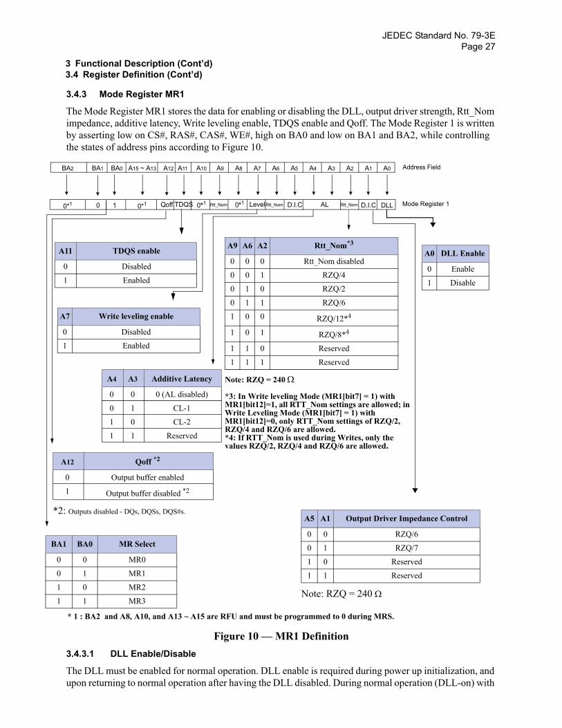
JEDEC Standard No. 79-3EPage 27
*
BA
0
0
1
1
3 Functional Description (Cont’d)3.4 Register Definition (Cont’d)
3.4.3 Mode Register MR1
The Mode Register MR1 stores the data for enabling or disabling the DLL, output driver strength, Rtt_Nom impedance, additive latency, Write leveling enable, TDQS enable and Qoff. The Mode Register 1 is written by asserting low on CS#, RAS#, CAS#, WE#, high on BA0 and low on BA1 and BA2, while controlling the states of address pins according to Figure 10.
Figure 10 — MR1 Definition3.4.3.1 DLL Enable/Disable
The DLL must be enabled for normal operation. DLL enable is required during power up initialization, and upon returning to normal operation after having the DLL disabled. During normal operation (DLL-on) with
Mode Register 1
Address FieldBA1 BA0 A11 A10 A9 A8 A7 A6 A5 A4 A3 A2 A1 A0
0 AL0*1 0*1
A15 ~ A13
1 Rtt_Nom
A0 DLL Enable
0 Enable
1 Disable
* 1 : BA2 and A8, A10, and A13 ~ A15 are RFU and must be programmed to 0 during MRS.
BA2
0*1
A12
Note: RZQ = 240 Ω
A5 A1 Output Driver Impedance Control
0 0 RZQ/6
0 1 RZQ/7
1 0 Reserved
1 1 Reserved
D.I.C DLL
Note: RZQ = 240 Ω
*3: In Write leveling Mode (MR1[bit7] = 1) with MR1[bit12]=1, all RTT_Nom settings are allowed; in Write Leveling Mode (MR1[bit7] = 1) with MR1[bit12]=0, only RTT_Nom settings of RZQ/2, RZQ/4 and RZQ/6 are allowed.*4: If RTT_Nom is used during Writes, only the values RZQ/2, RZQ/4 and RZQ/6 are allowed.
A9 A6 A2 Rtt_Nom*3
0 0 0 Rtt_Nom disabled
0 0 1 RZQ/4
0 1 0 RZQ/2
0 1 1 RZQ/6
1 0 0 RZQ/12*4
1 0 1 RZQ/8*4
1 1 0 Reserved
1 1 1 Reserved
A7 Write leveling enable
0 Disabled
1 Enabled
A4 A3 Additive Latency
0 0 0 (AL disabled)
0 1 CL-1
1 0 CL-2
1 1 Reserved
2: Outputs disabled - DQs, DQSs, DQS#s.
A12 Qoff *2
0 Output buffer enabled
1 Output buffer disabled *2
Qoff LevelTDQS 0*1 Rtt_Nom D.I.C
A11 TDQS enable
0 Disabled
1 Enabled
Rtt_Nom
1 BA0 MR Select
0 MR0
1 MR1
0 MR2
1 MR3

JEDEC Standard No. 79-3EPage 28
3.4 Register Definition (Cont’d)3.4.3 Mode Register MR1 (Cont’d)
MR1 (A0 = 0), the DLL is automatically disabled when entering Self-Refresh operation and is automatically re-enabled upon exit of Self-Refresh operation. Any time the DLL is enabled and subsequently reset, tDLLK clock cycles must occur before a Read or synchronous ODT command can be issued to allow time for the internal clock to be synchronized with the external clock. Failing to wait for synchronization to occur may result in a violation of the tDQSCK, tAON or tAOF parameters. During tDLLK, CKE must continu-ously be registered high. DDR3 SDRAM does not require DLL for any Write operation, except when RTT_WR is enabled and the DLL is required for proper ODT operation. For more detailed information on DLL Disable operation refer to “DLL-off Mode” on page 37.
The direct ODT feature is not supported during DLL-off mode. The on-die termination resistors must be disabled by continuously registering the ODT pin low and/or by programming the RTT_Nom bits MR1{A9,A6,A2} to {0,0,0} via a mode register set command during DLL-off mode.
The dynamic ODT feature is not supported at DLL-off mode. User must use MRS command to set Rtt_WR, MR2 {A10, A9} = {0,0}, to disable Dynamic ODT externally.
3.4.3.2 Output Driver Impedance Control
The output driver impedance of the DDR3 SDRAM device is selected by MR1 (bits A1 and A5) as shown in Figure 10.
3.4.3.3 ODT Rtt Values
DDR3 SDRAM is capable of providing two different termination values (Rtt_Nom and Rtt_WR). The nom-inal termination value Rtt_Nom is programmed in MR1. A separate value (Rtt_WR) may be programmed in MR2 to enable a unique RTT value when ODT is enabled during writes. The Rtt_WR value can be applied during writes even when Rtt_Nom is disabled.
3.4.3.4 Additive Latency (AL)
Additive Latency (AL) operation is supported to make command and data bus efficient for sustainable band-widths in DDR3 SDRAM. In this operation, the DDR3 SDRAM allows a read or write command (either with or without auto-precharge) to be issued immediately after the active command. The command is held for the time of the Additive Latency (AL) before it is issued inside the device. The Read Latency (RL) is controlled by the sum of the AL and CAS Latency (CL) register settings. Write Latency (WL) is controlled by the sum of the AL and CAS Write Latency (CWL) register settings. A summary of the AL register op-tions are shown in Table 4.
NOTE: AL has a value of CL - 1 or CL - 2 as per the CL values programmed in the MR0 register.
3.4.3.5 Write leveling
For better signal integrity, DDR3 memory module adopted fly-by topology for the commands, addresses, control signals, and clocks. The fly-by topology has the benefit of reducing the number of stubs and their length, but it also causes flight time skew between clock and strobe at every DRAM on the DIMM. This makes it difficult for the Controller to maintain tDQSS, tDSS, and tDSH specification. Therefore, the DDR3 SDRAM supports a ‘write leveling’ feature to allow the controller to compensate for skew. See 4.8 “Write Leveling” on page 42 for more details.
Table 4 — Additive Latency (AL) Settings
A4 A3 AL
0 0 0 (AL Disabled)0 1 CL - 11 0 CL - 21 1 Reserved
JEDEC Standard No. 79-3EPage 29
3.4 Register Definition (Cont’d)3.4.3 Mode Register MR1 (Cont’d
3.4.3.6 Output Disable
The DDR3 SDRAM outputs may be enabled/disabled by MR1 (bit A12) as shown in Figure 10. When this feature is enabled (A12 = 1), all output pins (DQs, DQS, DQS#, etc.) are disconnected from the device, thus removing any loading of the output drivers. This feature may be useful when measuring module power, for example. For normal operation, A12 should be set to ‘0’.
3.4.3.7 TDQS, TDQS#
TDQS (Termination Data Strobe) is a feature of X8 DDR3 SDRAM that provides additional termination resistance outputs that may be useful in some system configurations.
TDQS is not supported in X4 or X16 configurations. When enabled via the mode register, the same termi-nation resistance function is applied to the TDQS/TDQS# pins that is applied to the DQS/DQS# pins.
In contrast to the RDQS function of DDR2 SDRAM, TDQS provides the termination resistance function only. The data strobe function of RDQS is not provided by TDQS.
The TDQS and DM functions share the same pin. When the TDQS function is enabled via the mode register, the DM function is not supported. When the TDQS function is disabled, the DM function is provided and the TDQS# pin is not used. See Table 5 for details.
The TDQS function is available in X8 DDR3 SDRAM only and must be disabled via the mode register A11=0 in MR1 for X4 and X16 configurations.
NOTE 1 If TDQS is enabled, the DM function is disabled.NOTE 2 When not used, TDQS function can be disabled to save termination power.NOTE 3 TDQS function is only available for X8 DRAM and must be disabled for X4 and X16.
Table 5 — TDQS, TDQS# Function Matrix
MR1 (A11) DM / TDQS NU / TDQS
0 (TDQS Disabled) DM Hi-Z1 (TDQS Enabled) TDQS TDQS#
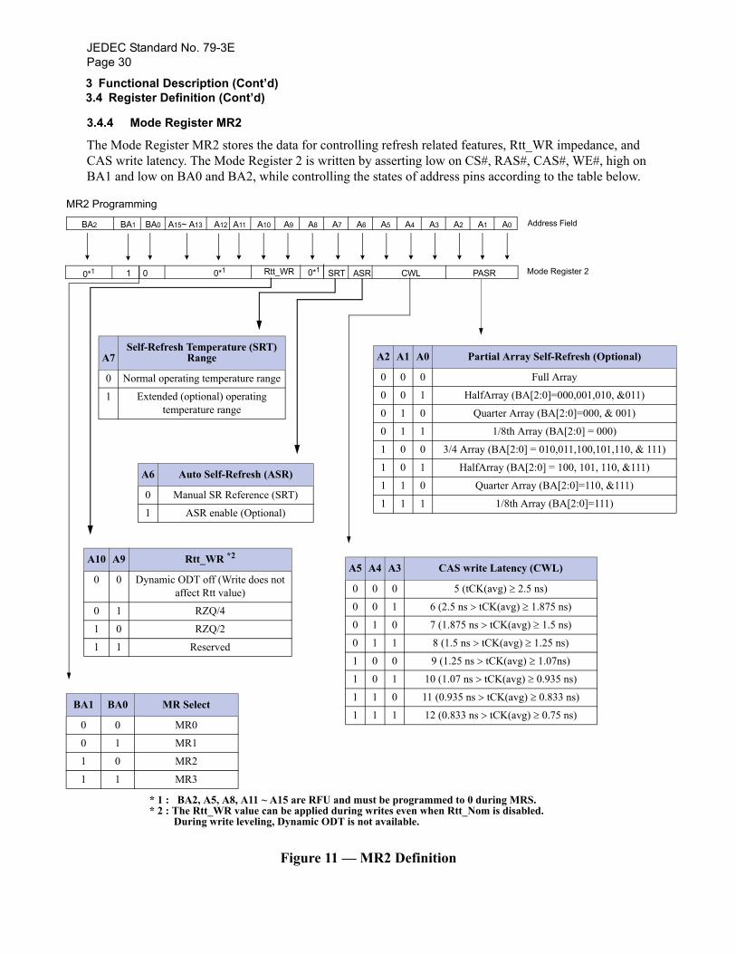
JEDEC Standard No. 79-3EPage 30
MR
)
B
3 Functional Description (Cont’d)3.4 Register Definition (Cont’d)
3.4.4 Mode Register MR2
The Mode Register MR2 stores the data for controlling refresh related features, Rtt_WR impedance, and CAS write latency. The Mode Register 2 is written by asserting low on CS#, RAS#, CAS#, WE#, high on BA1 and low on BA0 and BA2, while controlling the states of address pins according to the table below.
Figure 11 — MR2 Definition
2 Programming
Mode Register 2
Address FieldBA1 BA0 A11 A10 A9 A8 A7 A6 A5 A4 A3 A2 A1 A0
1
A15~ A13
0 0*1
BA2
0*1
A12
PASR
A2 A1 A0 Partial Array Self-Refresh (Optional)
0 0 0 Full Array
0 0 1 HalfArray (BA[2:0]=000,001,010, &011)
0 1 0 Quarter Array (BA[2:0]=000, & 001)
0 1 1 1/8th Array (BA[2:0] = 000)
1 0 0 3/4 Array (BA[2:0] = 010,011,100,101,110, & 111
1 0 1 HalfArray (BA[2:0] = 100, 101, 110, &111)
1 1 0 Quarter Array (BA[2:0]=110, &111)
1 1 1 1/8th Array (BA[2:0]=111)
* 1 : BA2, A5, A8, A11 ~ A15 are RFU and must be programmed to 0 during MRS.* 2 : The Rtt_WR value can be applied during writes even when Rtt_Nom is disabled.
During write leveling, Dynamic ODT is not available.
SRT ASR CWL
A5 A4 A3 CAS write Latency (CWL)
0 0 0 5 (tCK(avg) ≥ 2.5 ns)
0 0 1 6 (2.5 ns > tCK(avg) ≥ 1.875 ns)
0 1 0 7 (1.875 ns > tCK(avg) ≥ 1.5 ns)
0 1 1 8 (1.5 ns > tCK(avg) ≥ 1.25 ns)
1 0 0 9 (1.25 ns > tCK(avg) ≥ 1.07ns)
1 0 1 10 (1.07 ns > tCK(avg) ≥ 0.935 ns)
1 1 0 11 (0.935 ns > tCK(avg) ≥ 0.833 ns)
1 1 1 12 (0.833 ns > tCK(avg) ≥ 0.75 ns)
A7Self-Refresh Temperature (SRT)
Range
0 Normal operating temperature range
1 Extended (optional) operating temperature range
A6 Auto Self-Refresh (ASR)
0 Manual SR Reference (SRT)
1 ASR enable (Optional)
0*1Rtt_WR
A10 A9 Rtt_WR *2
0 0 Dynamic ODT off (Write does not affect Rtt value)
0 1 RZQ/4
1 0 RZQ/2
1 1 Reserved
A1 BA0 MR Select
0 0 MR0
0 1 MR1
1 0 MR2
1 1 MR3
JEDEC Standard No. 79-3EPage 31
3.4 Register Definition (Cont’d)3.4.4 Mode Register MR2 (Cont’d)
3.4.4.1 Partial Array Self-Refresh (PASR)
Optional in DDR3 SDRAM: Users should refer to the DRAM supplier data sheet and/or the DIMM SPD to determine if DDR3 SDRAM devices support the following options or requirements referred to in this ma-terial. If PASR (Partial Array Self-Refresh) is enabled, data located in areas of the array beyond the specified address range shown in Figure 11 will be lost if Self-Refresh is entered. Data integrity will be maintained if tREFI conditions are met and no Self-Refresh command is issued.
3.4.4.2 CAS Write Latency (CWL)
The CAS Write Latency is defined by MR2 (bits A3-A5), as shown in Figure 11. CAS Write Latency is the delay, in clock cycles, between the internal Write command and the availability of the first bit of input data. DDR3 SDRAM does not support any half-clock latencies. The overall Write Latency (WL) is defined as Additive Latency (AL) + CAS Write Latency (CWL); WL = AL + CWL. For more information on the sup-ported CWL and AL settings based on the operating clock frequency, refer to “Standard Speed Bins” on page 159. For detailed Write operation refer to “WRITE Operation” on page 68.
3.4.4.3 Auto Self-Refresh (ASR) and Self-Refresh Temperature (SRT)
Optional in DDR3 SDRAM: Users should refer to the DRAM supplier data sheet and/or the DIMM SPD to determine if DDR3 SDRAM devices support the following options or requirements referred to in this ma-terial. For more details refer to “Extended Temperature Usage” on page 46. DDR3 SDRAMs must support Self-Refresh operation at all supported temperatures. Applications requiring Self-Refresh operation in the Extended Temperature Range must use the optional ASR function or program the SRT bit appropriately.
3.4.4.4 Dynamic ODT (Rtt_WR)
DDR3 SDRAM introduces a new feature “Dynamic ODT”. In certain application cases and to further en-hance signal integrity on the data bus, it is desirable that the termination strength of the DDR3 SDRAM can be changed without issuing an MRS command. MR2 Register locations A9 and A10 configure the Dynamic ODT setings. In Write leveling mode, only RTT_Nom is available. For details on Dynamic ODT operation, refer to “Dynamic ODT” on page 94.
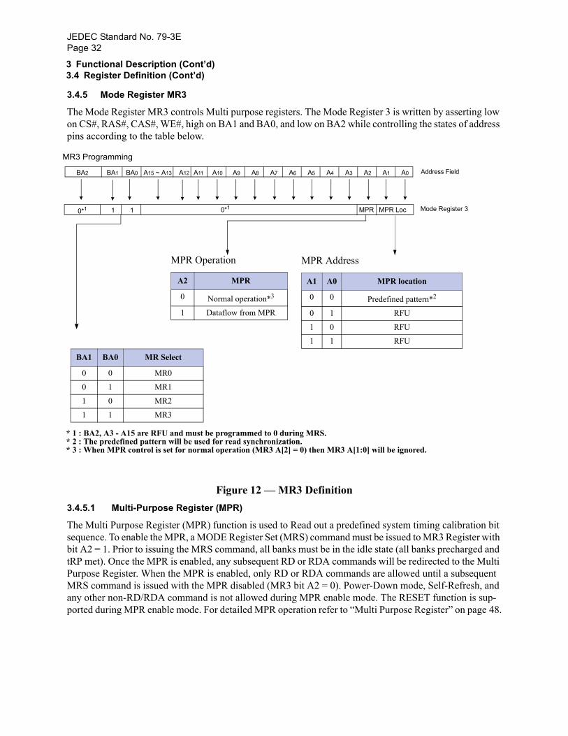
JEDEC Standard No. 79-3EPage 32
3 Functional Description (Cont’d)3.4 Register Definition (Cont’d)
3.4.5 Mode Register MR3
The Mode Register MR3 controls Multi purpose registers. The Mode Register 3 is written by asserting low on CS#, RAS#, CAS#, WE#, high on BA1 and BA0, and low on BA2 while controlling the states of address pins according to the table below.
Figure 12 — MR3 Definition3.4.5.1 Multi-Purpose Register (MPR)
The Multi Purpose Register (MPR) function is used to Read out a predefined system timing calibration bit sequence. To enable the MPR, a MODE Register Set (MRS) command must be issued to MR3 Register with bit A2 = 1. Prior to issuing the MRS command, all banks must be in the idle state (all banks precharged and tRP met). Once the MPR is enabled, any subsequent RD or RDA commands will be redirected to the Multi Purpose Register. When the MPR is enabled, only RD or RDA commands are allowed until a subsequent MRS command is issued with the MPR disabled (MR3 bit A2 = 0). Power-Down mode, Self-Refresh, and any other non-RD/RDA command is not allowed during MPR enable mode. The RESET function is sup-ported during MPR enable mode. For detailed MPR operation refer to “Multi Purpose Register” on page 48.
MR3 Programming
Mode Register 3
Address FieldBA1 BA0 A11 A10 A9 A8 A7 A6 A5 A4 A3 A2 A1 A0
1
A15 ~ A13
1 0*1
BA2
0*1
A12
MPR Address
A1 A0 MPR location
0 0 Predefined pattern*2
0 1 RFU
1 0 RFU
1 1 RFU
MPR Operation
A2 MPR
0 Normal operation*3
1 Dataflow from MPR
MPR Loc MPR
* 1 : BA2, A3 - A15 are RFU and must be programmed to 0 during MRS.* 2 : The predefined pattern will be used for read synchronization. * 3 : When MPR control is set for normal operation (MR3 A[2] = 0) then MR3 A[1:0] will be ignored.
BA1 BA0 MR Select
0 0 MR0
0 1 MR1
1 0 MR2
1 1 MR3
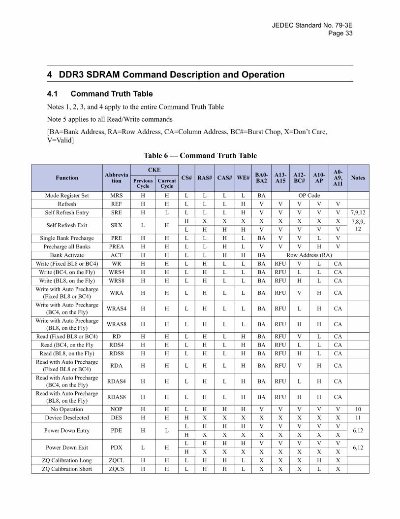
JEDEC Standard No. 79-3EPage 33
es
129,
S
WrWW
Wr
Wr
Wr
ReRR
Re
Re
Re
2
2
4 DDR3 SDRAM Command Description and Operation
4.1 Command Truth TableNotes 1, 2, 3, and 4 apply to the entire Command Truth Table
Note 5 applies to all Read/Write commands
[BA=Bank Address, RA=Row Address, CA=Column Address, BC#=Burst Chop, X=Don’t Care, V=Valid]
Table 6 — Command Truth Table
Function Abbreviation
CKECS# RAS# CAS# WE# BA0-
BA2A13-A15
A12-BC#
A10-AP
A0-A9, A11
NotPrevious Cycle
Current Cycle
Mode Register Set MRS H H L L L L BA OP CodeRefresh REF H H L L L H V V V V V
Self Refresh Entry SRE H L L L L H V V V V V 7,9,
Self Refresh Exit SRX L HH X X X X X X X X 7,8,
12L H H H V V V V Vingle Bank Precharge PRE H H L L H L BA V V L VPrecharge all Banks PREA H H L L H L V V V H V
Bank Activate ACT H H L L H H BA Row Address (RA)ite (Fixed BL8 or BC4) WR H H L H L L BA RFU V L CArite (BC4, on the Fly) WRS4 H H L H L L BA RFU L L CArite (BL8, on the Fly) WRS8 H H L H L L BA RFU H L CA
ite with Auto Precharge (Fixed BL8 or BC4) WRA H H L H L L BA RFU V H CA
ite with Auto Precharge (BC4, on the Fly) WRAS4 H H L H L L BA RFU L H CA
ite with Auto Precharge (BL8, on the Fly) WRAS8 H H L H L L BA RFU H H CA
ad (Fixed BL8 or BC4) RD H H L H L H BA RFU V L CAead (BC4, on the Fly RDS4 H H L H L H BA RFU L L CAead (BL8, on the Fly) RDS8 H H L H L H BA RFU H L CAad with Auto Precharge (Fixed BL8 or BC4) RDA H H L H L H BA RFU V H CA
ad with Auto Precharge (BC4, on the Fly) RDAS4 H H L H L H BA RFU L H CA
ad with Auto Precharge (BL8, on the Fly) RDAS8 H H L H L H BA RFU H H CA
No Operation NOP H H L H H H V V V V V 10Device Deselected DES H H H X X X X X X X X 11
Power Down Entry PDE H LL H H H V V V V V
6,1H X X X X X X X X
Power Down Exit PDX L HL H H H V V V V V
6,1H X X X X X X X X
ZQ Calibration Long ZQCL H H L H H L X X X H XZQ Calibration Short ZQCS H H L H H L X X X L X

JEDEC Standard No. 79-3EPage 34
f
H
de
ic
lf
d l-
e d
l
es
4 DDR3 SDRAM Command Description and Operation (Cont’d)4.1 Command Truth Table (Cont’d)
NOTE 1 All DDR3 SDRAM commands are defined by states of CS#, RAS#, CAS#, WE# and CKE at the rising edge othe clock. The MSB of BA, RA and CA are device density and configuration dependant.
NOTE 2 RESET# is Low enable command which will be used only for asynchronous reset so must be maintained HIGduring any function.
NOTE 3 Bank addresses (BA) determine which bank is to be operated upon. For (E)MRS BA selects an (Extended) MoRegister.
NOTE 4 “V” means “H or L (but a defined logic level)” and “X” means either “defined or undefined (like floating) loglevel”.
NOTE 5 Burst reads or writes cannot be terminated or interrupted and Fixed/on-the-Fly BL will be defined by MRS.NOTE 6 The Power Down Mode does not perform any refresh operation.NOTE 7 The state of ODT does not affect the states described in this table. The ODT function is not available during Se
Refresh.NOTE 8 Self Refresh Exit is asynchronous.NOTE 9 VREF(Both VrefDQ and VrefCA) must be maintained during Self Refresh operation. VrefDQ supply may be
turned OFF and VREFDQ may take any value between VSS and VDD during Self Refresh operation, providethat VrefDQ is valid and stable prior to CKE going back High and that first Write operation or first Write Leveing Activity may not occur earlier than 512 nCK after exit from Self Refresh.
NOTE 10 The No Operation command should be used in cases when the DDR3 SDRAM is in an idle or wait state. Thpurpose of the No Operation command (NOP) is to prevent the DDR3 SDRAM from registerng any unwantecommands between operations. A No Operation command will not terminate a pervious operation that is stilexecuting, such as a burst read or write cycle.
NOTE 11 The Deselect command performs the same function as No Operation command.NOTE 12 Refer to the CKE Truth Table for more detail with CKE transition.
Table 6 — Command Truth Table (Cont’d)
Function Abbreviation
CKECS# RAS# CAS# WE# BA0-
BA2A13-A15
A12-BC#
A10-AP
A0-A9, A11
NotPrevious Cycle
Current Cycle
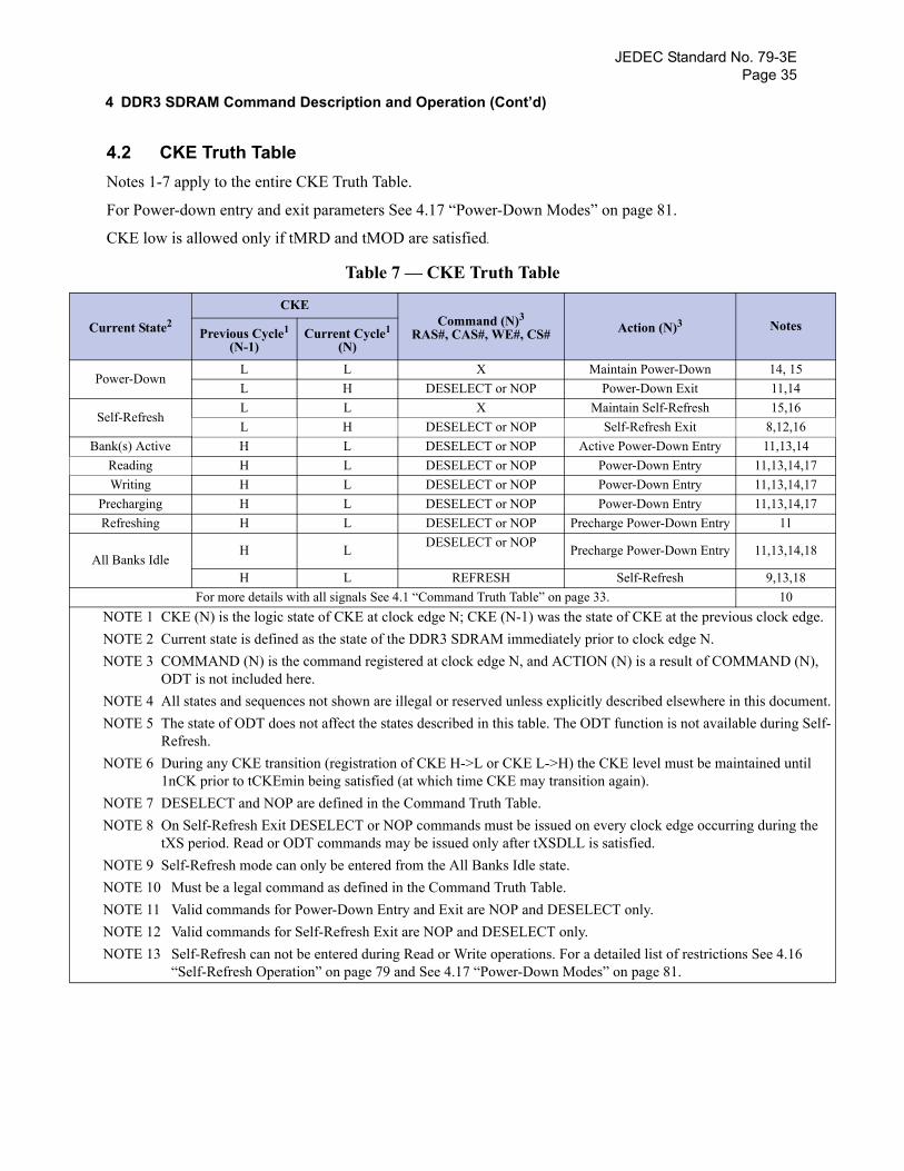
JEDEC Standard No. 79-3EPage 35
C
B
A
e.
,
nt.lf-
4 DDR3 SDRAM Command Description and Operation (Cont’d)
4.2 CKE Truth TableNotes 1-7 apply to the entire CKE Truth Table.
For Power-down entry and exit parameters See 4.17 “Power-Down Modes” on page 81.
CKE low is allowed only if tMRD and tMOD are satisfied.
Table 7 — CKE Truth Table
urrent State2CKE
Command (N)3
RAS#, CAS#, WE#, CS# Action (N)3 NotesPrevious Cycle1
(N-1)Current Cycle1
(N)
Power-DownL L X Maintain Power-Down 14, 15L H DESELECT or NOP Power-Down Exit 11,14
Self-RefreshL L X Maintain Self-Refresh 15,16L H DESELECT or NOP Self-Refresh Exit 8,12,16
ank(s) Active H L DESELECT or NOP Active Power-Down Entry 11,13,14Reading H L DESELECT or NOP Power-Down Entry 11,13,14,17Writing H L DESELECT or NOP Power-Down Entry 11,13,14,17
Precharging H L DESELECT or NOP Power-Down Entry 11,13,14,17Refreshing H L DESELECT or NOP Precharge Power-Down Entry 11
ll Banks IdleH L DESELECT or NOP Precharge Power-Down Entry 11,13,14,18
H L REFRESH Self-Refresh 9,13,18For more details with all signals See 4.1 “Command Truth Table” on page 33. 10
NOTE 1 CKE (N) is the logic state of CKE at clock edge N; CKE (N-1) was the state of CKE at the previous clock edgNOTE 2 Current state is defined as the state of the DDR3 SDRAM immediately prior to clock edge N.NOTE 3 COMMAND (N) is the command registered at clock edge N, and ACTION (N) is a result of COMMAND (N)
ODT is not included here.NOTE 4 All states and sequences not shown are illegal or reserved unless explicitly described elsewhere in this documeNOTE 5 The state of ODT does not affect the states described in this table. The ODT function is not available during Se
Refresh.NOTE 6 During any CKE transition (registration of CKE H->L or CKE L->H) the CKE level must be maintained until
1nCK prior to tCKEmin being satisfied (at which time CKE may transition again).NOTE 7 DESELECT and NOP are defined in the Command Truth Table.NOTE 8 On Self-Refresh Exit DESELECT or NOP commands must be issued on every clock edge occurring during the
tXS period. Read or ODT commands may be issued only after tXSDLL is satisfied.NOTE 9 Self-Refresh mode can only be entered from the All Banks Idle state.NOTE 10 Must be a legal command as defined in the Command Truth Table.NOTE 11 Valid commands for Power-Down Entry and Exit are NOP and DESELECT only.NOTE 12 Valid commands for Self-Refresh Exit are NOP and DESELECT only.NOTE 13 Self-Refresh can not be entered during Read or Write operations. For a detailed list of restrictions See 4.16
“Self-Refresh Operation” on page 79 and See 4.17 “Power-Down Modes” on page 81.
JEDEC Standard No. 79-3EPage 36
o
be ed el-
n
s
C
4 DDR3 SDRAM Command Description and Operation (Cont’d)4.2 CKE Truth Table (Cont’d)
4.3 No OPeration (NOP) CommandThe No OPeration (NOP) command is used to instruct the selected DDR3 SDRAM to perform a NOP (CS# LOW and RAS#, CAS#, and WE# HIGH). This prevents unwanted commands from being registered during idle or wait states. Operations already in progress are not affected.
4.4 Deselect CommandThe DESELECT function (CS# HIGH) prevents new commands from being executed by the DDR3 SDRAM. The DDR3 SDRAM is effectively deselected. Operations already in progress are not affected.
NOTE 14 The Power-Down does not perform any refresh operations.NOTE 15 “X” means “don’t care“ (including floating around VREF) in Self-Refresh and Power-Down. It also applies t
Address pins.NOTE 16 VREF (Both Vref_DQ and Vref_CA) must be maintained during Self-Refresh operation.VrefDQ supply may
turned OFF and VREFDQ may take any value between VSS and VDD during Self Refresh operation, providthat VrefDQ is valid and stable prior to CKE going back High and that first Write operation or first Write Leving Activity may not occur earlier than 512 nCK after exit from Self Refresh.
NOTE 17 If all banks are closed at the conclusion of the read, write or precharge command, then Precharge Power-Dowis entered, otherwise Active Power-Down is entered.
NOTE 18 ‘Idle state’ is defined as all banks are closed (tRP, tDAL, etc. satisfied), no data bursts are in progress, CKE ihigh, and all timings from previous operations are satisfied (tMRD, tMOD, tRFC, tZQinit, tZQoper, tZQCS,etc.) as well as all Self-Refresh exit and Power-Down Exit parameters are satisfied (tXS, tXP, tXPDLL, etc).
Table 7 — CKE Truth Table (Cont’d)
urrent State2
CKECommand (N)3
RAS#, CAS#, WE#, CS# Action (N)3 NotesPrevious Cycle1
(N-1)Current Cycle1
(N)

JEDEC Standard No. 79-3EPage 37
ARE
DQS,
DQS, D
DQS, D
4 DDR3 SDRAM Command Description and Operation (Cont’d)
4.5 DLL-off ModeDDR3 DLL-off mode is entered by setting MR1 bit A0 to “1”; this will disable the DLL for subsequent operations until A0 bit is set back to “0”. The MR1 A0 bit for DLL control can be switched either during initialization or later. Refer to “Input clock frequency change” on page 40
The DLL-off Mode operations listed below are an optional feature for DDR3. The maximum clock fre-quency for DLL-off Mode is specified by the parameter tCKDLL_OFF. There is no minimum frequency limit besides the need to satisfy the refresh interval, tREFI.
Due to latency counter and timing restrictions, only one value of CAS Latency (CL) in MR0 and CAS Write Latency (CWL) in MR2 are supported. The DLL-off mode is only required to support setting of both CL=6 and CWL=6.
DLL-off mode will affect the Read data Clock to Data Strobe relationship (tDQSCK), but not the Data Strobe to Data relationship (tDQSQ, tQH). Special attention is needed to line up Read data to controller time domain.
Comparing with DLL-on mode, where tDQSCK starts from the rising clock edge (AL+CL) cycles after the Read command, the DLL-off mode tDQSCK starts (AL+CL - 1) cycles after the read command. Another difference is that tDQSCK may not be small compared to tCK (it might even be larger than tCK) and the difference between tDQSCKmin and tDQSCKmax is significantly larger than in DLL-on mode. tDQSCK(DLL_off) values are vendor specific.
The timing relations on DLL-off mode READ operation are shown in the following Timing Diagram (CL=6, BL=8):
Figure 13 — DLL-off mode READ Timing Operation
T0 T1 T2 T3 T4 T5 T6 T7 T8 T9 T10
DON’T CTRANSITIONING DATA
Bank,Col b
DIN
b + 3DIN
b + 2DIN
b + 1DIN
bDIN
b + 7DIN
b + 6DIN
b + 5DIN
b + 4
NOPREAD NOP NOP NOP NOP NOP NOP NOP NOP NOP
CK
CK#
COMMAND
ADDRESS
DIN
b + 3DIN
b + 2DIN
b + 1DIN
bDIN
b + 7DIN
b + 6DIN
b + 5DIN
b + 4
DIN
b + 3DIN
b + 2DIN
b + 1DIN
bDIN
b + 7DIN
b + 6DIN
b + 5DIN
b + 4DQ (DLL_on)
DQS# (DLL_on)
DQ (DLL_off)
QS# (DLL_off)
DQ (DLL_off)
QS# (DLL_off)
tDQSCK(DLL_off)_min
tDQSCK(DLL_off)_max
RL (DLL_off) = AL + (CL - 1) = 5
RL (DLL_on) = AL + CL = 6 (CL = 6, AL = 0)
CL = 6
Note: The tDQSCK is used here for DQS, DQS# and DQ to have a simplified diagram; the DLL_off shift will affect both timings in the same way and the skew between all DQ and DQS, DQS# signals will still be tDQSQ.

JEDEC Standard No. 79-3EPage 38
COMM
4 DDR3 SDRAM Command Description and Operation (Cont’d)
4.6 DLL on/off switching procedureDDR3 DLL-off mode is entered by setting MR1 bit A0 to “1”; this will disable the DLL for subsequent operations until A0 bit is set back to “0”.
4.6.1 DLL “on” to DLL “off” Procedure
To switch from DLL “on” to DLL “off” requires the frequency to be changed during Self-Refresh, as out-lined in the following procedure:
1. Starting from Idle state (All banks pre-charged, all timings fulfilled, and DRAMs On-die Termination resistors, RTT, must be in high impedance state before MRS to MR1 to disable the DLL.)
2. Set MR1 bit A0 to “1” to disable the DLL.3. Wait tMOD.4. Enter Self Refresh Mode; wait until (tCKSRE) is satisfied. 5. Change frequency, in guidance with “Input clock frequency change” on page 40.6. Wait until a stable clock is available for at least (tCKSRX) at DRAM inputs.7. Starting with the Self Refresh Exit command, CKE must continuously be registered HIGH until all
tMOD timings from any MRS command are satisfied. In addition, if any ODT features were enabled in the mode registers when Self Refresh mode was entered, the ODT signal must continuously be regis-tered LOW until all tMOD timings from any MRS command are satisfied. If both ODT features were disabled in the mode registers when Self Refresh mode was entered, ODT signal can be registered LOW or HIGH.
8. Wait tXS, then set Mode Registers with appropriate values (especially an update of CL, CWL and WR may be necessary. A ZQCL command may also be issued after tXS).
9. Wait for tMOD, then DRAM is ready for next command.
Figure 14 — DLL Switch Sequence from DLL-on to DLL-off
T0 T1 Ta0 Ta1 Tb0 Tc0
tMOD (4)(1) tCKSRE
tCKESR
tXS
Td0 Td1 Te0 Te1 Tf0
CK
CK#
ODT
CKE
SRE (3) NOPMRS (2)AND NOP
tMOD
SRX (6) MRS (7) VALID (8)
VALID (8)
VALID (8)
NOP NOP
1. Starting with Idle State, RTT in Hi-Z state2. Disable DLL by setting MR1 Bit A0 to 13. Enter SR4. Change Frequency5. Clock must be stable tCKSRX6. Exit SR7. Update Mode registers with DLL off parameters setting8. Any valid command
DON’T CARE()()
()()
TIME BREAK
ODT: Static LOW in case RTT_Nom and RTT_WR is enabled, otherwise static Low or High
NOTES:
tCKSRX (5)
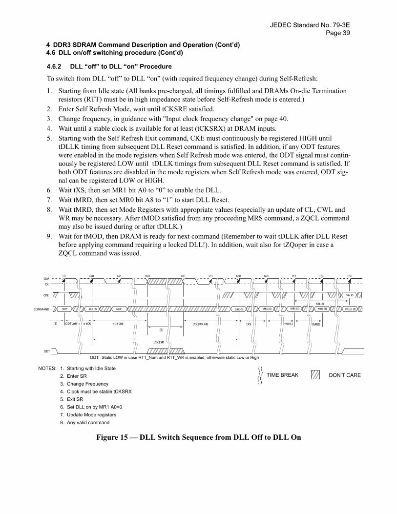
JEDEC Standard No. 79-3EPage 39
COMM
EN
4 DDR3 SDRAM Command Description and Operation (Cont’d)4.6 DLL on/off switching procedure (Cont’d)
4.6.2 DLL “off” to DLL “on” Procedure
To switch from DLL “off” to DLL “on” (with required frequency change) during Self-Refresh:
1. Starting from Idle state (All banks pre-charged, all timings fulfilled and DRAMs On-die Termination resistors (RTT) must be in high impedance state before Self-Refresh mode is entered.)
2. Enter Self Refresh Mode, wait until tCKSRE satisfied.3. Change frequency, in guidance with "Input clock frequency change" on page 40.4. Wait until a stable clock is available for at least (tCKSRX) at DRAM inputs.5. Starting with the Self Refresh Exit command, CKE must continuously be registered HIGH until
tDLLK timing from subsequent DLL Reset command is satisfied. In addition, if any ODT features were enabled in the mode registers when Self Refresh mode was entered, the ODT signal must contin-uously be registered LOW until tDLLK timings from subsequent DLL Reset command is satisfied. If both ODT features are disabled in the mode registers when Self Refresh mode was entered, ODT sig-nal can be registered LOW or HIGH.
6. Wait tXS, then set MR1 bit A0 to “0” to enable the DLL.7. Wait tMRD, then set MR0 bit A8 to “1” to start DLL Reset.8. Wait tMRD, then set Mode Registers with appropriate values (especially an update of CL, CWL and
WR may be necessary. After tMOD satisfied from any proceeding MRS command, a ZQCL command may also be issued during or after tDLLK.)
9. Wait for tMOD, then DRAM is ready for next command (Remember to wait tDLLK after DLL Reset before applying command requiring a locked DLL!). In addition, wait also for tZQoper in case a ZQCL command was issued.
Figure 15 — DLL Switch Sequence from DLL Off to DLL On
T0 Ta0 Ta1 Tb0 Tc0 Tc1
(3)
(1) tCKSRE tCKSRX (4)
tCKESR
tXS
Td0 Te0 Tf1 Tg0 Th0
CK
CK#
ODT
CKE
SRE (2) NOPAND NOP
tMRD
tDLLK
tMRD
SRX (5) MRS (6) MRS (7) MRS (8) VALID (9)
VALID
1. Starting with Idle State2. Enter SR3. Change Frequency4. Clock must be stable tCKSRX5. Exit SR6. Set DLL on by MR1 A0=07. Update Mode registers 8. Any valid command
DON’T CAR()()
()()
TIME BREAK
ODT: Static LOW in case RTT_Nom and RTT_WR is enabled, otherwise static Low or High
ODTLoff + 1 x tCK
OTES:
JEDEC Standard No. 79-3EPage 40
4 DDR3 SDRAM Command Description and Operation (Cont’d)
4.7 Input clock frequency changeOnce the DDR3 SDRAM is initialized, the DDR3 SDRAM requires the clock to be “stable” during almost all states of normal operation. This means that, once the clock frequency has been set and is to be in the “stable state”, the clock period is not allowed to deviate except for what is allowed for by the clock jitter and SSC (spread spectrum clocking) specifications.
The input clock frequency can be changed from one stable clock rate to another stable clock rate under two conditions: (1) Self-Refresh mode and (2) Precharge Power-down mode. Outside of these two modes, it is illegal to change the clock frequency.
For the first condition, once the DDR3 SDRAM has been successfully placed in to Self-Refresh mode and tCKSRE has been satisfied, the state of the clock becomes a don’t care. Once a don’t care, changing the clock frequency is permissible, provided the new clock frequency is stable prior to tCKSRX. When enter-ing and exiting Self-Refresh mode for the sole purpose of changing the clock frequency, the Self-Refresh entry and exit specifications must still be met as outlined in See 4.16 “Self-Refresh Operation” on page 79. The DDR3 SDRAM input clock frequency is allowed to change only within the minimum and maximum operating frequency specified for the particular speed grade. Any frequency change below the minimum operating frequency would require the use of DLL_on- mode -> DLL_off -mode transition sequence, refer to “DLL on/off switching procedure” on page 38.
The second condition is when the DDR3 SDRAM is in Precharge Power-down mode (either fast exit mode or slow exit mode). If the RTT_NOM feature was enabled in the mode register prior to entering Precharge power down mode, the ODT signal must continuously be registered LOW ensuring RTT is in an off state. If the RTT_NOM feature was disabled in the mode register prior to entering Precharge power down mode, RTT will remain in the off state. The ODT signal can be registered either LOW or HIGH in this case. A minimum of tCKSRE must occur after CKE goes LOW before the clock frequency may change. The DDR3 SDRAM input clock frequency is allowed to change only within the minimum and maximum oper-ating frequency specified for the particular speed grade. During the input clock frequency change, ODT and CKE must be held at stable LOW levels. Once the input clock frequency is changed, stable new clocks must be provided to the DRAM tCKSRX before Precharge Power-down may be exited; after Precharge Power-down is exited and tXP has expired, the DLL must be RESET via MRS. Depending on the new clock frequency, additional MRS commands may need to be issued to appropriately set the WR, CL, and CWL with CKE continuously registered high. During DLL re-lock period, ODT must remain LOW and CKE must remain HIGH. After the DLL lock time, the DRAM is ready to operate with new clock fre-quency. This process is depicted in Figure 16 on page 41.
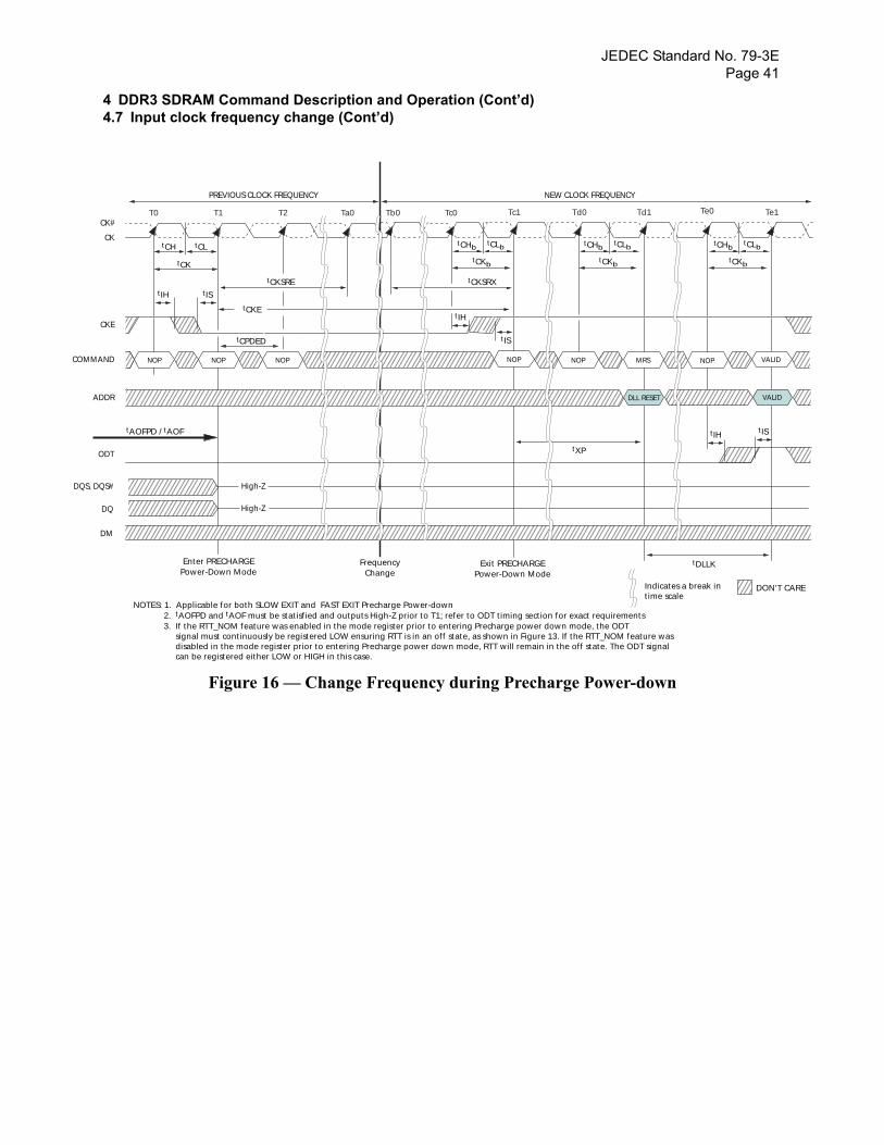
JEDEC Standard No. 79-3EPage 41
COMM
DQS,
RE
4 DDR3 SDRAM Command Description and Operation (Cont’d)4.7 Input clock frequency change (Cont’d)
Figure 16 — Change Frequency during Precharge Power-down
CK
CK#
AND NOPNOPNOP
ADDR
CKE
DQ
DM
DQS#
NOP
tCK
Enter PRECHARGEPower-Down Mode
Exit PRECHARGEPower-Down Mode
T0 T1 Ta0 Tc0Tb0T2
DON’T CA
tCKE
tXP
MRS
DLL RESET
VALID
VALID
NOP
tCH
tIH tIS
tCL
Tc1 Td0 Te1Td1
tCKSRE tCKSRX
tCHbtCLb
tCKb
tCHbtCLb
tCKb
tCHbtCLb
tCKb
tCPDED
ODT
NOP
Te0
PREVIOUS CLOCK FREQUENCY NEW CLOCK FREQUENCY
FrequencyChange
High-Z
High-Z
Indicates a break in time scale
tIHtIS
tIH
tIS
tDLLK
NOTES: 1. Applicable for both SLOW EXIT and FAST EXIT Precharge Power-down 2. tAOFPD and tAOF must be statisfied and outputs High-Z prior to T1; refer to ODT timing section for exact requirements 3. If the RTT_NOM feature was enabled in the mode register prior to entering Precharge power down mode, the ODT signal must continuously be registered LOW ensuring RTT is in an off state, as shown in Figure 13. If the RTT_NOM feature was disabled in the mode register prior to entering Precharge power down mode, RTT will remain in the off state. The ODT signal can be registered either LOW or HIGH in this case.
tAOFPD / tAOF
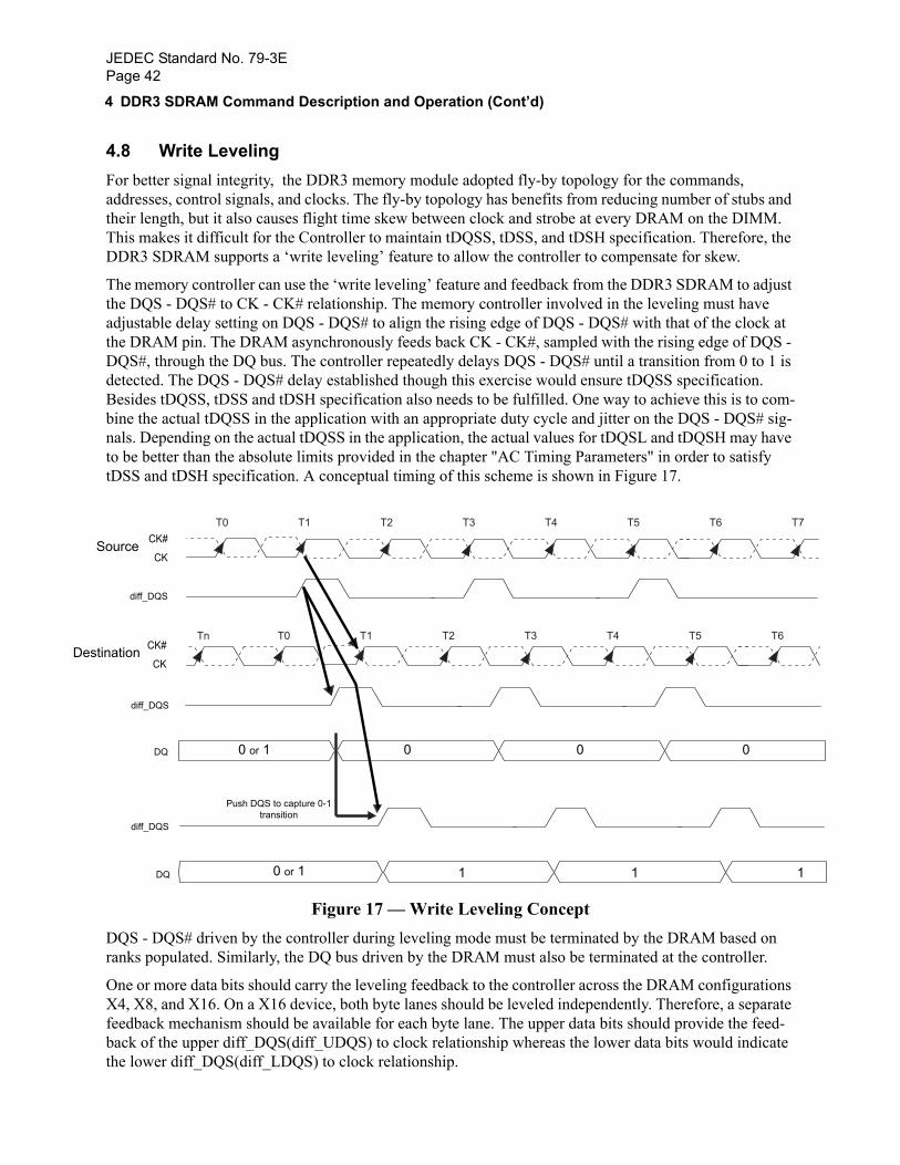
JEDEC Standard No. 79-3EPage 42
Des
4 DDR3 SDRAM Command Description and Operation (Cont’d)
4.8 Write LevelingFor better signal integrity, the DDR3 memory module adopted fly-by topology for the commands, addresses, control signals, and clocks. The fly-by topology has benefits from reducing number of stubs and their length, but it also causes flight time skew between clock and strobe at every DRAM on the DIMM. This makes it difficult for the Controller to maintain tDQSS, tDSS, and tDSH specification. Therefore, the DDR3 SDRAM supports a ‘write leveling’ feature to allow the controller to compensate for skew.
The memory controller can use the ‘write leveling’ feature and feedback from the DDR3 SDRAM to adjust the DQS - DQS# to CK - CK# relationship. The memory controller involved in the leveling must have adjustable delay setting on DQS - DQS# to align the rising edge of DQS - DQS# with that of the clock at the DRAM pin. The DRAM asynchronously feeds back CK - CK#, sampled with the rising edge of DQS - DQS#, through the DQ bus. The controller repeatedly delays DQS - DQS# until a transition from 0 to 1 is detected. The DQS - DQS# delay established though this exercise would ensure tDQSS specification. Besides tDQSS, tDSS and tDSH specification also needs to be fulfilled. One way to achieve this is to com-bine the actual tDQSS in the application with an appropriate duty cycle and jitter on the DQS - DQS# sig-nals. Depending on the actual tDQSS in the application, the actual values for tDQSL and tDQSH may have to be better than the absolute limits provided in the chapter "AC Timing Parameters" in order to satisfy tDSS and tDSH specification. A conceptual timing of this scheme is shown in Figure 17.
Figure 17 — Write Leveling ConceptDQS - DQS# driven by the controller during leveling mode must be terminated by the DRAM based on ranks populated. Similarly, the DQ bus driven by the DRAM must also be terminated at the controller.
One or more data bits should carry the leveling feedback to the controller across the DRAM configurations X4, X8, and X16. On a X16 device, both byte lanes should be leveled independently. Therefore, a separate feedback mechanism should be available for each byte lane. The upper data bits should provide the feed-back of the upper diff_DQS(diff_UDQS) to clock relationship whereas the lower data bits would indicate the lower diff_DQS(diff_LDQS) to clock relationship.
CK
CK#Source
diff_DQS
diff_DQS
diff_DQS
DQ
DQ
CK
CK#tination
Push DQS to capture 0-1transition
T0 T1 T2 T3 T4 T5 T6 T7
T0 T1 T2 T3 T4 T5 T6Tn
1 1
0
1
000 or 1
0 or 1
JEDEC Standard No. 79-3EPage 43
4 DDR3 SDRAM Command Description and Operation (Cont’d)4.8 Write Leveling (Cont’d)
4.8.1 DRAM setting for write leveling & DRAM termination function in that mode
DRAM enters into Write leveling mode if A7 in MR1 set ’High’ and after finishing leveling, DRAM exits from write leveling mode if A7 in MR1 set ’Low’ (Table 8). Note that in write leveling mode, only DQS/DQS# terminations are activated and deactivated via ODT pin, unlike normal operation (Table 9).
Table 8 — MR setting involved in the leveling procedure
Table 9 — DRAM termination function in the leveling mode
NOTE: In Write Leveling Mode with its output buffer disabled (MR1[bit7] = 1 withMR1[bit12] = 1) all RTT_Nom settings are allowed; in Write Leveling Modewith its output buffer enabled (MR1[bit7] = 1 with MR1[bit12] = 0) onlyRTT_Nom settings of RZQ/2, RZQ/4 and RZQ/6 are allowed.
4.8.2 Procedure Description
The Memory controller initiates Leveling mode of all DRAMs by setting bit 7 of MR1 to 1. When entering write leveling mode, the DQ pins are in undefined driving mode. During write leveling mode, only NOP or DESELECT commands are allowed, as well as an MRS command to change Qoff bit (MR1[A12]) and an MRS command to exit write leveling (MR1[A7]). Upon exiting write leveling mode, the MRS command performing the exit (MR1[A7]=0) may also change MR1 bits of A12-A11, A9, A6-A5, and A2-A1. Since the controller levels one rank at a time, the output of other ranks must be disabled by setting MR1 bit A12 to 1. The Controller may assert ODT after tMOD, at which time the DRAM is ready to accept the ODT signal.
The Controller may drive DQS low and DQS# high after a delay of tWLDQSEN, at which time the DRAM has applied on-die termination on these signals. After tDQSL and tWLMRD, the controller provides a sin-gle DQS, DQS# edge which is used by the DRAM to sample CK - CK# driven from controller. tWLMRD(max) timing is controller dependent.
DRAM samples CK - CK# status with rising edge of DQS - DQS# and provides feedback on all the DQ bits asynchronously after tWLO timing. Either one or all data bits ("prime DQ bit(s)") provide the leveling feedback. The DRAM's remaining DQ bits are driven Low statically after the first sampling procedure. There is a DQ output uncertainty of tWLOE defined to allow mismatch on DQ bits. The tWLOE period is defined from the transition of the earliest DQ bit to the corresponding transition of the latest DQ bit. There are no read strobes (DQS/DQS#) needed for these DQs. Controller samples incoming DQ and decides to increment or decrement DQS - DQS# delay setting and launches the next DQS/DQS# pulse after some time, which is controller dependent. Once a 0 to 1 transition is detected, the controller locks DQS - DQS# delay setting and write leveling is achieved for the device. Figure 18 describes the timing diagram and parameters for the overall Write Leveling procedure.
Function MR1 Enable Disable
Write leveling enable A7 1 0
Output buffer mode (Qoff) A12 0 1
ODT pin @DRAM DQS/DQS# termination DQs termination
De-asserted Off Off
Asserted On Off
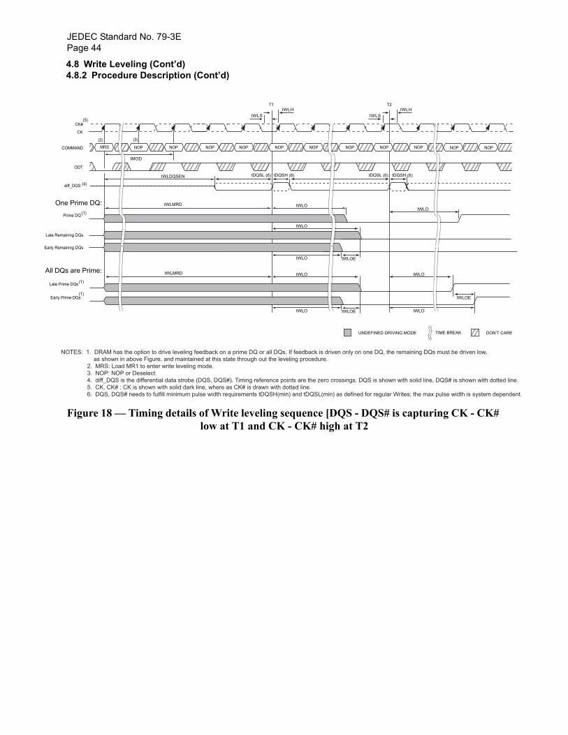
JEDEC Standard No. 79-3EPage 44
Early
Late P
ne.
ent.
O
Late Re
Early Re
All D
4.8 Write Leveling (Cont’d)4.8.2 Procedure Description (Cont’d)
Figure 18 — Timing details of Write leveling sequence [DQS - DQS# is capturing CK - CK# low at T1 and CK - CK# high at T2
tMOD
tWLDQSEN
tWLMRD
tWLH
tDQSH (6)tDQSL (6) tDQSH (6)tDQSL (6)
tWLOE
tWLStWLH
tWLS
NOP NOP NOP
CK
CK#
COMMAND
T1 T2
Prime DQs
ODT
rime DQs
diff_DQS
NOP NOPMRS NOP NOP NOP NOP NOP NOP NOP NOP NOP
(2) (3)
(4)
(5)
(1)
(1)
NOTES: 1. DRAM has the option to drive leveling feedback on a prime DQ or all DQs. If feedback is driven only on one DQ, the remaining DQs must be driven low, as shown in above Figure, and maintained at this state through out the leveling procedure. 2. MRS: Load MR1 to enter write leveling mode. 3. NOP: NOP or Deselect. 4. diff_DQS is the differential data strobe (DQS, DQS#). Timing reference points are the zero crossings. DQS is shown with solid line, DQS# is shown with dotted li 5. CK, CK# : CK is shown with solid dark line, where as CK# is drawn with dotted line. 6. DQS, DQS# needs to fulfill minimum pulse width requirements tDQSH(min) and tDQSL(min) as defined for regular Writes; the max pulse width is system depend
DON’T CAREUNDEFINED DRIVING MODE()()
()()
TIME BREAK
tWLMRDne Prime DQ: tWLOtWLO
maining DQs
tWLO
tWLO
Prime DQ(1)
maining DQs
tWLOE
tWLO
tWLO
tWLOE
tWLO
tWLO
Qs are Prime:
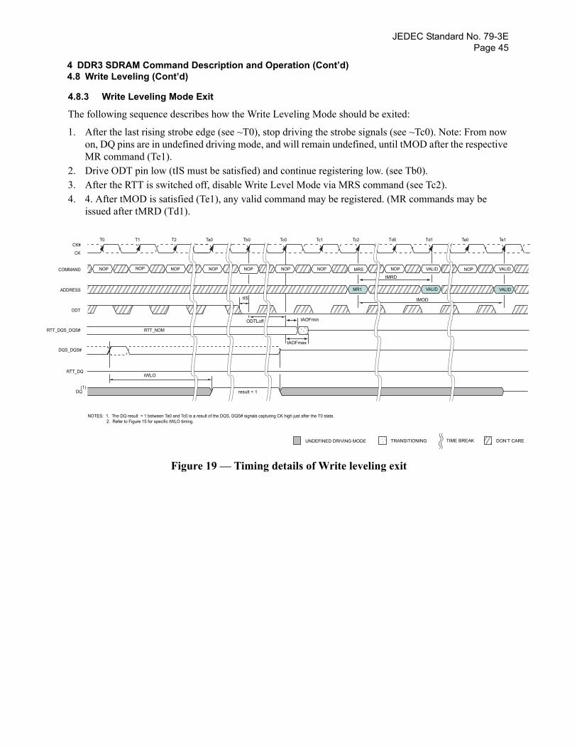
JEDEC Standard No. 79-3EPage 45
C
RTT_D
D
E
4 DDR3 SDRAM Command Description and Operation (Cont’d)4.8 Write Leveling (Cont’d)
4.8.3 Write Leveling Mode Exit
The following sequence describes how the Write Leveling Mode should be exited:
1. After the last rising strobe edge (see ~T0), stop driving the strobe signals (see ~Tc0). Note: From now on, DQ pins are in undefined driving mode, and will remain undefined, until tMOD after the respective MR command (Te1).
2. Drive ODT pin low (tIS must be satisfied) and continue registering low. (see Tb0).3. After the RTT is switched off, disable Write Level Mode via MRS command (see Tc2).4. 4. After tMOD is satisfied (Te1), any valid command may be registered. (MR commands may be
issued after tMRD (Td1).
Figure 19 — Timing details of Write leveling exit
tMOD
tWLO
ODTLoff
tIS
tMRD
CK = ‘0’
NOP NOP NOP
CK
T0 T1 T2 Ta0 Tb0 Tc0 Tc1 Tc2 Td0 Td1 Te0 Te1CK#
OMMAND
ODT
QS_DQS#
RTT_DQ
DQ
QS_DQS#
NOPNOPNOP NOP NOP NOP NOP MRS NOP NOP
NOPADDRESS MR1
VALID VALID
VALID VALID
result = 1
DON’T CARTRANSITIONING()()
()()
TIME BREAK
RTT_NOM
NOTES: 1. The DQ result = 1 between Ta0 and Tc0 is a result of the DQS, DQS# signals capturing CK high just after the T0 state. 2. Refer to Figure 15 for specific tWLO timing.
UNDEFINED DRIVING MODE
tAOFmax
tAOFmin
(1)
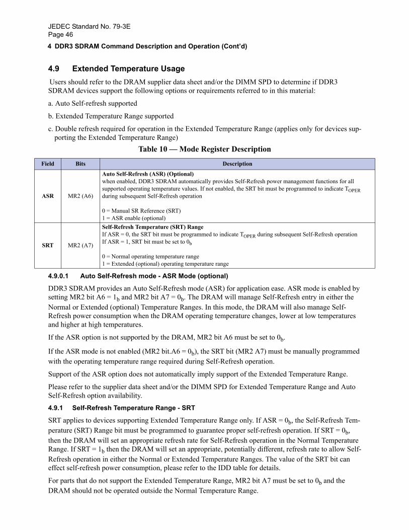
JEDEC Standard No. 79-3EPage 46
F
A
S
4 DDR3 SDRAM Command Description and Operation (Cont’d)
4.9 Extended Temperature Usage Users should refer to the DRAM supplier data sheet and/or the DIMM SPD to determine if DDR3 SDRAM devices support the following options or requirements referred to in this material:
a. Auto Self-refresh supported
b. Extended Temperature Range supported
c. Double refresh required for operation in the Extended Temperature Range (applies only for devices sup-porting the Extended Temperature Range)
4.9.0.1 Auto Self-Refresh mode - ASR Mode (optional)
DDR3 SDRAM provides an Auto Self-Refresh mode (ASR) for application ease. ASR mode is enabled by setting MR2 bit A6 = 1b and MR2 bit A7 = 0b. The DRAM will manage Self-Refresh entry in either the Normal or Extended (optional) Temperature Ranges. In this mode, the DRAM will also manage Self-Refresh power consumption when the DRAM operating temperature changes, lower at low temperatures and higher at high temperatures.
If the ASR option is not supported by the DRAM, MR2 bit A6 must be set to 0b.
If the ASR mode is not enabled (MR2 bit.A6 = 0b), the SRT bit (MR2 A7) must be manually programmed with the operating temperature range required during Self-Refresh operation.
Support of the ASR option does not automatically imply support of the Extended Temperature Range.
Please refer to the supplier data sheet and/or the DIMM SPD for Extended Temperature Range and Auto Self-Refresh option availability.
4.9.1 Self-Refresh Temperature Range - SRT
SRT applies to devices supporting Extended Temperature Range only. If ASR = 0b, the Self-Refresh Tem-perature (SRT) Range bit must be programmed to guarantee proper self-refresh operation. If SRT = 0b, then the DRAM will set an appropriate refresh rate for Self-Refresh operation in the Normal Temperature Range. If SRT = 1b then the DRAM will set an appropriate, potentially different, refresh rate to allow Self-Refresh operation in either the Normal or Extended Temperature Ranges. The value of the SRT bit can effect self-refresh power consumption, please refer to the IDD table for details.
For parts that do not support the Extended Temperature Range, MR2 bit A7 must be set to 0b and the DRAM should not be operated outside the Normal Temperature Range.
Table 10 — Mode Register Description
ield Bits Description
SR MR2 (A6)
Auto Self-Refresh (ASR) (Optional)when enabled, DDR3 SDRAM automatically provides Self-Refresh power management functions for all supported operating temperature values. If not enabled, the SRT bit must be programmed to indicate TOPER during subsequent Self-Refresh operation
0 = Manual SR Reference (SRT)1 = ASR enable (optional)
RT MR2 (A7)
Self-Refresh Temperature (SRT) Range If ASR = 0, the SRT bit must be programmed to indicate TOPER during subsequent Self-Refresh operationIf ASR = 1, SRT bit must be set to 0b
0 = Normal operating temperature range1 = Extended (optional) operating temperature range
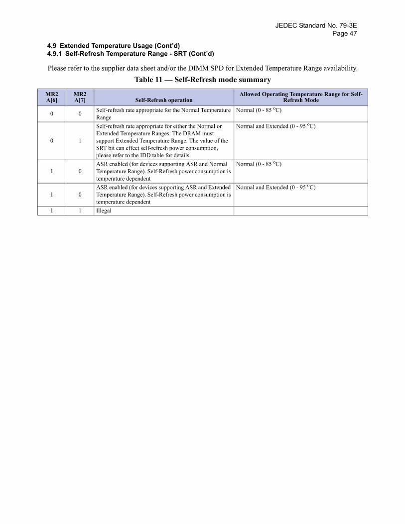
JEDEC Standard No. 79-3EPage 47
4.9 Extended Temperature Usage (Cont’d)4.9.1 Self-Refresh Temperature Range - SRT (Cont’d)
Please refer to the supplier data sheet and/or the DIMM SPD for Extended Temperature Range availability.Table 11 — Self-Refresh mode summary
MR2A[6]
MR2A[7] Self-Refresh operation
Allowed Operating Temperature Range for Self-Refresh Mode
0 0 Self-refresh rate appropriate for the Normal Temperature Range
Normal (0 - 85 oC)
0 1
Self-refresh rate appropriate for either the Normal or Extended Temperature Ranges. The DRAM must support Extended Temperature Range. The value of the SRT bit can effect self-refresh power consumption, please refer to the IDD table for details.
Normal and Extended (0 - 95 oC)
1 0ASR enabled (for devices supporting ASR and Normal Temperature Range). Self-Refresh power consumption is temperature dependent
Normal (0 - 85 oC)
1 0ASR enabled (for devices supporting ASR and Extended Temperature Range). Self-Refresh power consumption is temperature dependent
Normal and Extended (0 - 95 oC)
1 1 Illegal
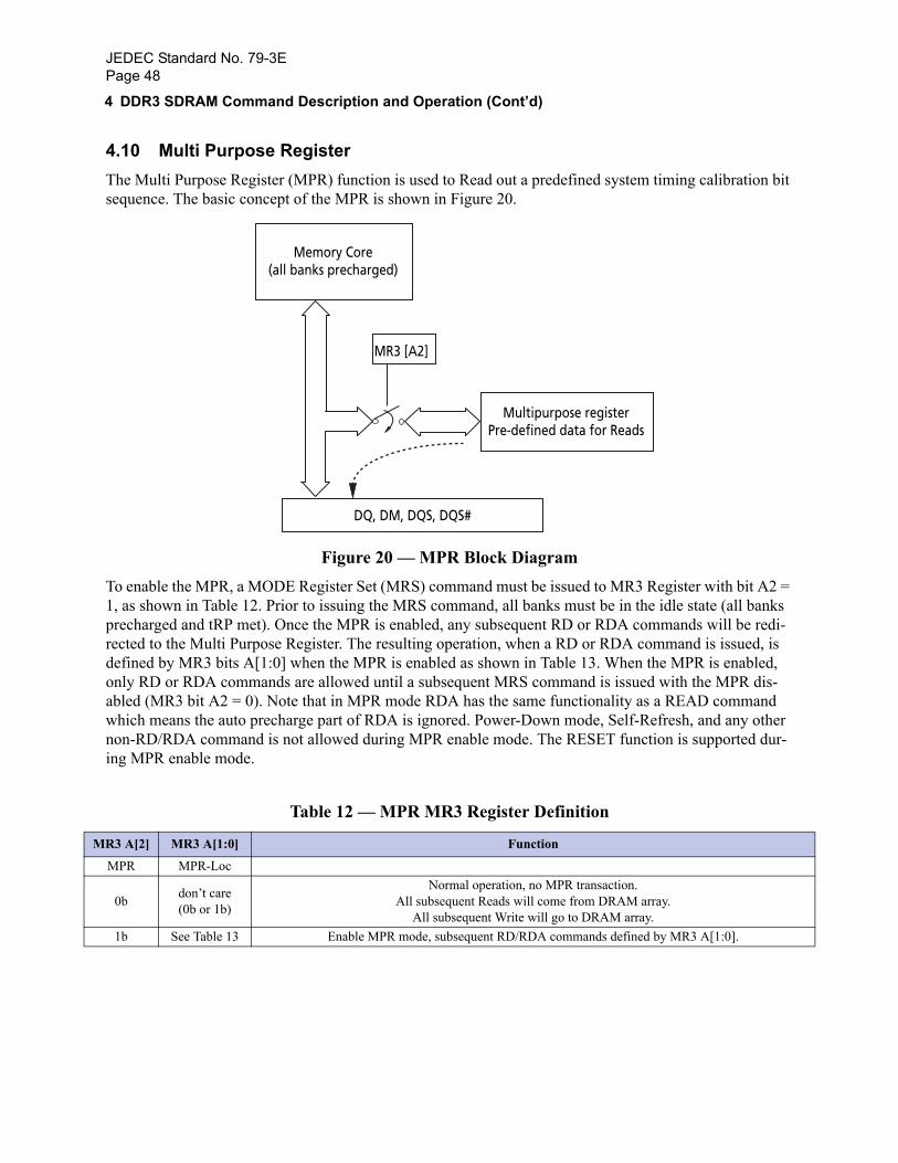
JEDEC Standard No. 79-3EPage 48
4 DDR3 SDRAM Command Description and Operation (Cont’d)
4.10 Multi Purpose RegisterThe Multi Purpose Register (MPR) function is used to Read out a predefined system timing calibration bit sequence. The basic concept of the MPR is shown in Figure 20.
Figure 20 — MPR Block DiagramTo enable the MPR, a MODE Register Set (MRS) command must be issued to MR3 Register with bit A2 = 1, as shown in Table 12. Prior to issuing the MRS command, all banks must be in the idle state (all banks precharged and tRP met). Once the MPR is enabled, any subsequent RD or RDA commands will be redi-rected to the Multi Purpose Register. The resulting operation, when a RD or RDA command is issued, is defined by MR3 bits A[1:0] when the MPR is enabled as shown in Table 13. When the MPR is enabled, only RD or RDA commands are allowed until a subsequent MRS command is issued with the MPR dis-abled (MR3 bit A2 = 0). Note that in MPR mode RDA has the same functionality as a READ command which means the auto precharge part of RDA is ignored. Power-Down mode, Self-Refresh, and any other non-RD/RDA command is not allowed during MPR enable mode. The RESET function is supported dur-ing MPR enable mode.
Table 12 — MPR MR3 Register Definition
MR3 A[2] MR3 A[1:0] Function
MPR MPR-Loc
0b don’t care(0b or 1b)
Normal operation, no MPR transaction.All subsequent Reads will come from DRAM array.
All subsequent Write will go to DRAM array.1b See Table 13 Enable MPR mode, subsequent RD/RDA commands defined by MR3 A[1:0].
Memory Core(all banks precharged)
MR3 [A2]
DQ, DM, DQS, DQS#
Multipurpose registerPre-defined data for Reads
JEDEC Standard No. 79-3EPage 49
4 DDR3 SDRAM Command Description and Operation (Cont’d)4.10 Multi Purpose Register (Cont’d)
4.10.1 MPR Functional Description
• One bit wide logical interface via all DQ pins during READ operation.• Register Read on x4:
• DQ[0] drives information from MPR. • DQ[3:1] either drive the same information as DQ[0], or they drive 0b.
• Register Read on x8: • DQ[0] drives information from MPR. • DQ[7:1] either drive the same information as DQ[0], or they drive 0b.
• Register Read on x16: • DQL[0] and DQU[0] drive information from MPR. • DQL[7:1] and DQU[7:1] either drive the same information as DQL[0], or they drive 0b.
• Addressing during for Multi Purpose Register reads for all MPR agents: • BA[2:0]: don’t care• A[1:0]: A[1:0] must be equal to ‘00’b. Data read burst order in nibble is fixed• A[2]: For BL=8, A[2] must be equal to 0b, burst order is fixed to [0,1,2,3,4,5,6,7], *) For Burst
Chop 4 cases, the burst order is switched on nibble base A[2]=0b, Burst order: 0,1,2,3 *) A[2]=1b, Burst order: 4,5,6,7 *)
• A[9:3]: don’t care• A10/AP: don’t care• A12/BC: Selects burst chop mode on-the-fly, if enabled within MR0.• A11, A13,... (if available): don’t care
• Regular interface functionality during register reads:• Support two Burst Ordering which are switched with A2 and A[1:0]=00b.• Support of read burst chop (MRS and on-the-fly via A12/BC) • All other address bits (remaining column address bits including A10, all bank address bits) will be
ignored by the DDR3 SDRAM.• Regular read latencies and AC timings apply.• DLL must be locked prior to MPR Reads.
NOTE: *) Burst order bit 0 is assigned to LSB and burst order bit 7 is assigned toMSB of the selected MPR agent.
JEDEC Standard No. 79-3EPage 50
MR
4 DDR3 SDRAM Command Description and Operation (Cont’d)4.10 Multi Purpose Register (Cont’d)
4.10.2 MPR Register Address Definition
Table 13 provides an overview of the available data locations, how they are addressed by MR3 A[1:0] dur-ing a MRS to MR3, and how their individual bits are mapped into the burst order bits during a Multi Pur-pose Register Read.
4.10.3 Relevant Timing Parameters
The following AC timing parameters are important for operating the Multi Purpose Register: tRP, tMRD, tMOD, and tMPRR. For more details refer to “Electrical Characteristics & AC Timing for DDR3-800 to DDR3-2133” on page 157.
4.10.4 Protocol Example
Protocol Example (This is one example):
Read out predetermined read-calibration pattern.
Description: Multiple reads from Multi Purpose Register, in order to do system level read timing calibra-tion based on predetermined and standardized pattern.
Protocol Steps:
• Precharge All.• Wait until tRP is satisfied.• MRS MR3, Opcode “A2 = 1b“ and “A[1:0] = 00b“
• Redirect all subsequent reads into the Multi Purpose Register, and load Pre-defined pattern into MPR. • Wait until tMRD and tMOD are satisfied (Multi Purpose Register is then ready to be read). During the
period MR3 A2 =1, no data write operation is allowed. • Read:
• A[1:0] = ‘00’b (Data burst order is fixed starting at nibble, always 00b here)• A[2] = ‘0’b (For BL=8, burst order is fixed as 0,1,2,3,4,5,6,7)• A12/BC = 1 (use regular burst length of 8)• All other address pins (including BA[2:0] and A10/AP): don’t care
Table 13 — MPR MR3 Register Definition
3 A[2] MR3 A[1:0] Function Burst Length
Read Address A[2:0] Burst Order and Data Pattern
1b 00b Read Predefined Pattern for System Calibration
BL8 000b Burst order 0,1,2,3,4,5,6,7Pre-defined Data Pattern [0,1,0,1,0,1,0,1]
BC4 000b Burst order 0,1,2,3Pre-defined Data Pattern [0,1,0,1]
BC4 100b Burst order 4,5,6,7Pre-defined Data Pattern [0,1,0,1]
1b 01b RFUBL8 000b Burst order 0,1,2,3,4,5,6,7BC4 000b Burst order 0,1,2,3BC4 100b Burst order 4,5,6,7
1b 10b RFUBL8 000b Burst order 0,1,2,3,4,5,6,7BC4 000b Burst order 0,1,2,3BC4 100b Burst order 4,5,6,7
1b 11b RFUBL8 000b Burst order 0,1,2,3,4,5,6,7BC4 000b Burst order 0,1,2,3BC4 100b Burst order 4,5,6,7
NOTE: Burst order bit 0 is assigned to LSB and the burst order bit 7 is assigned to MSB of theselected MPR agent.

JED
EC
Standard No. 79-3EPage 51
• Aft• Me• Aft• MR
• A• Wa• Con
readout
3
0
00
0
0
0
0
MRS NOP NOP VALID
CK
CK#
COMMAND
DQ
DQS, DQS#
A[9:3]
BA
A[1:0]
A[2]
A10, AP
A12, BC#
A[15:13]
A[11]
tMOD
NO
VALID
DON’T CARE
()()
()
TIME BREAK
Tc7 Tc8 Tc9 Td
4.10M
ulti Purpose Register (C
ont’d)4.10.4
Protocol Example C
ont’d)
er RL = AL + CL, DRAM bursts out the predefined Read Calibration Pattern.mory controller repeats these calibration reads until read data capture at memory controller is optimized.er end of last MPR read burst, wait until tMPRR is satisfied.S MR3, Opcode “A2 = 0b“ and “A[1:0] = valid data but value are don’t care“ll subsequent read and write accesses will be regular reads and writes from/to the DRAM array.it until tMRD and tMOD are satisfied.tinue with “regular” DRAM commands, like activate a memory bank for regular read or write access,...
Figure 21 — MPR Readout of predefined pattern, BL8 fixed burst order, single
MRSPREA READ
3 VALID
0
0
0
1
00
01
0
0
0
NOPNOP NOP NOP NOP NOP NOP NOP
tRP
RL
tMOD tMPRR
TES: 1. RD with BL8 either by MRS or OTF.
2. Memory Controller must drive 0 on A[2:0].
VALID
VALID
VALID
VALID1
VALID
()
(1)
(2)
(2)
T0 Ta Tb0 Tb1 Tc0 Tc1 Tc2 Tc3 Tc4 Tc5 Tc6
JED
EC
Standard No. 79-3E
Page 52
ack readout
Tc8 Tc9 Tc10 Td
3
0
00
0
0
0
0
NOP NOP MRS VALID
CK
CK#
COMMAND
DQ
DQS, DQS#
A[9:3]
BA
A[1:0]
A[2]
A10AP
A12,BC#
A[15:13]
A[11]
tMODtMPRR
NOT
VALID
DON’T CARE
()
)
TIME BREAK
4.10M
ulti Purpose Register (C
ont’d)4.10.4
Protocol Example C
ont’d)
Figure 22 — MPR Readout of predefined pattern, BL8 fixed burst order, back-to-b
T0 Ta Tb Tc0 Tc1 Tc2 Tc3 Tc4 Tc5 Tc6 Tc7
MRSPREA READ
3 VALID
02
0
02
0
0
1
00
01
0
0
0
READ NOP NOP NOP NOP NOP NOP NOP
tRP
RL
RL
tMOD tCCD
ES: 1. RD with BL8 either by MRS or OTF.
2. Memory Controller must drive 0 on A[2:0].
VALID
VALID
VALID
VALID
VALID
VALID VALID
VALID
VALID
VALID
VALID
()
()(
(1)(1)
(1)(1)
(2)(2)
(2)(2)
JED
EC
Standard No. 79-3EPage 53
nibble
3
0
00
0
0
0
0
MRS NOP NOP VALID
CK
CK#
COMMAND
DQ
DQS, DQS#
A[9:3]
BA
A[1:0]
A[2]
A10AP
A12,BC#
A[15:13]
A[11]
tMOD
NOTES
VALID
DON’T CARETIME BREAK
Tc8 Tc9 Tc10 Td
4.10M
ulti Purpose Register (C
ont’d)4.10.4
Protocol Example C
ont’d)
Figure 23 — MPR Readout predefined pattern, BC4, lower nibble then upper
T0 Ta Tb
MRSPREA READ READ
3 VALID
0
1
0
0
0
1
00
01
0
0
0
NOP NOP NOP NOP NOP NOP NOP
tRF
RL
RL
tMOD tCCD tMPRR
: 1. RD with BC4 either by MRS or OTF.
2. Memory Controller must drive 0 on A[1:0].
3. A[2]=0 selects lower 4 nibble bits 0....3.
4. A[2]=1 selects upper 4 nibble bits 4....7.
VALID
VALID
VALID
VALID
VALID
VALID VALID
VALID
VALID
VALID
VALID
()()
()()
(1) (1)
(1) (1)
(2) (2)
(3) (4)
Tc0 Tc1 Tc2 Tc3 Tc4 Tc5 Tc6 Tc7
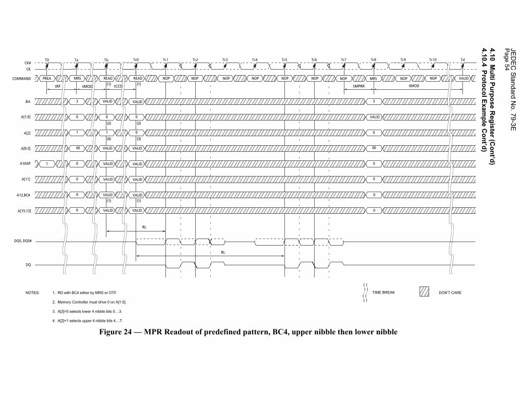
JED
EC
Standard No. 79-3E
Page 54
r nibble
3
0
00
0
0
0
0
MRS NOP NOP VALID
CK
CK#
COMMAND
DQ
DQS, DQS#
A[9:3]
BA
A[1:0]
A[2]
A10AP
A12,BC#
A[15:13]
A[11]
tMOD
NOTES:
VALID
DON’T CARETIME BREAK
Tc8 Tc9 Tc10 Td
4.10M
ulti Purpose Register (C
ont’d)4.10.4
Protocol Example C
ont’d)
Figure 24 — MPR Readout of predefined pattern, BC4, upper nibble then lowe
T0 Ta Tb
MRSPREA READ
3 VALID
0
0
0
1
0
1
00
01
0
0
0
READ NOP NOP NOP NOP NOP NOP NOP
tRF
RL
RL
tMOD tCCD tMPRR
1. RD with BC4 either by MRS or OTF.
2. Memory Controller must drive 0 on A[1:0].
3. A[2]=0 selects lower 4 nibble bits 0....3.
4. A[2]=1 selects upper 4 nibble bits 4....7.
VALID
VALID
VALID
VALID
VALID
VALID VALID
VALID
VALID
VALID
VALID
()()
()()
Tc0 Tc1 Tc2 Tc3 Tc4 Tc5 Tc6 Tc7
(1) (1)
(1) (1)
(4) (3)
(2) (2)
JEDEC Standard No. 79-3EPage 55
4 DDR3 SDRAM Command Description and Operation (Cont’d)
4.11 ACTIVE CommandThe ACTIVE command is used to open (or activate) a row in a particular bank for a subsequent access. The value on the BA0-BA2 inputs selects the bank, and the address provided on inputs A0-A15 selects the row. This row remains active (or open) for accesses until a precharge command is issued to that bank. A PRECHARGE command must be issued before opening a different row in the same bank.
4.12 PRECHARGE CommandThe PRECHARGE command is used to deactivate the open row in a particular bank or the open row in all banks. The bank(s) will be available for a subsequent row activation a specified time (tRP) after the PRE-CHARGE command is issued, except in the case of concurrent auto precharge, where a READ or WRITE command to a different bank is allowed as long as it does not interrupt the data transfer in the current bank and does not violate any other timing parameters. Once a bank has been precharged, it is in the idle state and must be activated prior to any READ or WRITE commands being issued to that bank. A PRE-CHARGE command is allowed if there is no open row in that bank (idle state) or if the previously open row is already in the process of precharging. However, the precharge period will be determined by the last PRECHARGE command issued to the bank.
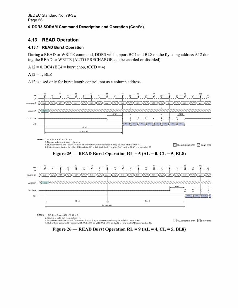
JEDEC Standard No. 79-3EPage 56
4 DDR3 SDRAM Command Description and Operation (Cont’d)
4.13 READ Operation4.13.1 READ Burst Operation
During a READ or WRITE command, DDR3 will support BC4 and BL8 on the fly using address A12 dur-ing the READ or WRITE (AUTO PRECHARGE can be enabled or disabled).
A12 = 0, BC4 (BC4 = burst chop, tCCD = 4)
A12 = 1, BL8
A12 is used only for burst length control, not as a column address.
Figure 25 — READ Burst Operation RL = 5 (AL = 0, CL = 5, BL8)
Figure 26 — READ Burst Operation RL = 9 (AL = 4, CL = 5, BL8)
NOTES: 1. BL8, RL = 5, AL = 0, CL = 5. 2. DOUT n = data-out from column n. 3. NOP commands are shown for ease of illustration; other commands may be valid at these times. 4. BL8 setting activated by either MR0[A1:0 = 00] or MR0[A1:0 = 01] and A12 = 1 during READ command at T0.
RL = AL + CL
T0 T1 T2 T3 T4 T5 T6 T7 T8 T9 T10
DON’T CARETRANSITIONING DATA
Bank,Col n
NOPREAD NOPNOP NOP NOP NOP NOP NOP NOP NOP
CK
CK#
COMMAND3
DQ2
DQS, DQS#
ADDRESS4
CL = 5
DOUT
n + 3DOUT
n + 2DOUT
n + 1DOUT
n
tRPRE
DOUT
n + 7DOUT
n + 6DOUT
n + 5DOUT n + 4
tRPST
NOTES: 1. BL8, RL = 9, AL = (CL - 1), CL = 5. 2. DOUT n = data-out from column n. 3. NOP commands are shown for ease of illustration; other commands may be valid at these times. 4. BL8 setting activated by either MR0[A1:0 = 00] or MR0[A1:0 = 01] and A12 = 1 during READ command at T0.
DOUT
n + 2DOUT
n + 1DOUT
n
RL = AL + CL
T0 T1 T2 T3 T4 T5 T6 T7 T8 T9
tRPRE
T10
DON’T CARETRANSITIONING DATA
Bank,Col n
NOPREAD NOPNOP NOP NOP NOP NOP NOP NOP NOP
CK
CK#
COMMAND3
DQ2
DQS, DQS#
ADDRESS4
AL = 4 CL = 5

JEDEC Standard No. 79-3EPage 57
4 DDR3 SDRAM Command Description and Operation (Cont’d)4.13 READ Operation (Cont’d)
4.13.2 READ Timing Definitions
Read timing is shown in Figure 27 and is applied when the DLL is enabled and locked.
Rising data strobe edge parameters:
• tDQSCK min/max describes the allowed range for a rising data strobe edge relative to CK, CK#.• tDQSCK is the actual position of a rising strobe edge relative to CK, CK#.• tQSH describes the DQS, DQS# differential output high time.• tDQSQ describes the latest valid transition of the associated DQ pins.• tQH describes the earliest invalid transition of the associated DQ pins.
Falling data strobe edge parameters:
• tQSL describes the DQS, DQS# differential output low time.• tDQSQ describes the latest valid transition of the associated DQ pins.• tQH describes the earliest invalid transition of the associated DQ pins.
tDQSQ; both rising/falling edges of DQS, no tAC defined.
Figure 27 — READ Timing Definition
CK
DQS
DQS
tDQSCK
Rising Strobe Region
tQSH tQSL
Rising Strobe Region
tDQSCK,MAX
tDQSCK
tDQSCK,MAX
tDQSCK,MINtDQSCK,MIN
tQH
tDQSQ
tQH
tDQSQ
AssociatedDQ Pins
CK#

JEDEC Standard No. 79-3EPage 58
DQEarly
CL
DQSLate S
NO ing
4.13 READ Operation (Cont’d)4.13.2 READ Timing Definitions (Cont’d)
4.13.2.1 READ Timing; Clock to Data Strobe relationship
Clock to Data Strobe relationship is shown in Figure 28 and is applied when the DLL is enabled and locked.
Rising data strobe edge parameters:
• tDQSCK min/max describes the allowed range for a rising data strobe edge relative to CK, CK#.• tDQSCK is the actual position of a rising strobe edge relative to CK, CK#.• tQSH describes the data strobe high pulse width.
Falling data strobe edge parameters:
• tQSL describes the data strobe low pulse width.
tLZ(DQS), tHZ(DQS) for preamble/postam ble (see 4.13.2.3 and Figure 30)
Figure 28 — Clock to Data Strobe Relationship
RL Measuredto this point
S,DQS# Strobe
K/CLK#
tDQSCK (min)
tLZ(DQS)min
tHZ(DQS)min
,DQS#trobe
tDQSCK (max)tLZ(DQS)max
tHZ(DQS)max
tDQSCK (min)tDQSCK (min)tDQSCK (min)
tDQSCK (max)tDQSCK (max)tDQSCK (max)
tRPRE
tQSH tQSL tQSH tQSLtQSL
tQSL tQSL
tQSH
tQSH tQSH
Bit 0 Bit 1 Bit 2 Bit 7
tRPRE
Bit 0 Bit 1 Bit 2 Bit 7Bit 6Bit 3 Bit 4 Bit 5
Bit 6Bit 4Bit 3 Bit 5
tRPST
tRPST
TES: 1. Within a burst, rising strobe edge is not necessarily fixed to be always at tDQSCK(min) or tDQSCK(max). Instead, rising strobe edge can vary between tDQSCK(min) and tDQSCK(max). 2. Notwithstanding note 1, a rising strobe edge with tDQSCK(max) at T(n) can not be immediately followed by a rising strobe edge with tDQSCK(min) at T(n+1). This is because other tim relationships (tQSH, tQSL) exist: if tDQSCK(n+1) < 0: tDQSCK(n) < 1.0 tCK - (tQSHmin + tQSLmin) - | tDQSCK(n+1) |3. The DQS, DQS# differential output high time is defined by tQSH and the DQS, DQS# differential output low time is defined by tQSL.4. Likewise, tLZ(DQS)min and tHZ(DQS)min are not tied to tDQSCKmin (early strobe case) and tLZ(DQS)max and tHZ(DQS)max are not tied to tDQSCKmax (late strobe case).
5. The minimum pulse width of read preamble is defined by tRPRE(min). 6. The maximum read postamble is bound by tDQSCK(min) plus tQSH(min) on the left side and tHZDSQ(max) on the right side. 7. The minimum pulse width of read postamble is defined by tRPST(min). 8. The maximum read preamble is bound by tLZDQS(min) on the left side and tDQSCK(max) on the right side.
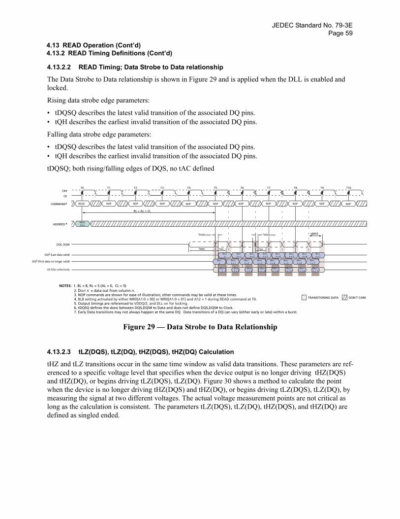
JEDEC Standard No. 79-3EPage 59
DQ2 (Fir
ARE
4.13 READ Operation (Cont’d)4.13.2 READ Timing Definitions (Cont’d)
4.13.2.2 READ Timing; Data Strobe to Data relationship
The Data Strobe to Data relationship is shown in Figure 29 and is applied when the DLL is enabled and locked.
Rising data strobe edge parameters:
• tDQSQ describes the latest valid transition of the associated DQ pins.• tQH describes the earliest invalid transition of the associated DQ pins.
Falling data strobe edge parameters:
• tDQSQ describes the latest valid transition of the associated DQ pins.• tQH describes the earliest invalid transition of the associated DQ pins.
tDQSQ; both rising/falling edges of DQS, no tAC defined
Figure 29 — Data Strobe to Data Relationship
4.13.2.3 tLZ(DQS), tLZ(DQ), tHZ(DQS), tHZ(DQ) Calculation
tHZ and tLZ transitions occur in the same time window as valid data transitions. These parameters are ref-erenced to a specific voltage level that specifies when the device output is no longer driving tHZ(DQS) and tHZ(DQ), or begins driving tLZ(DQS), tLZ(DQ). Figure 30 shows a method to calculate the point when the device is no longer driving tHZ(DQS) and tHZ(DQ), or begins driving tLZ(DQS), tLZ(DQ), by measuring the signal at two different voltages. The actual voltage measurement points are not critical as long as the calculation is consistent. The parameters tLZ(DQS), tLZ(DQ), tHZ(DQS), and tHZ(DQ) are defined as singled ended.
RL = AL + CL
T0 T1 T2 T3 T4 T5 T6 T7 T8 T9 T10
Bank,Col n
tRPST
NOPREAD NOPNOP NOP NOP NOP NOP NOP NOP NOP
CK
CK#
COMMAND3
ADDRESS 4
tQH
tDQSQ (max)tDQSQ (max)
DQS, DQS#
DQ2 (Last data valid)
st data no longer valid)
All DQs collectively
tQH
DOUT
n + 3DOUT
n + 2DOUT
n + 1DOUT
nDOUT
n + 7DOUT
n + 6DOUT
n + 5DOUT n + 4
DOUT
n + 2DOUT
n + 1DOUT
n + 7DOUT
n + 6DOUT
n + 5DOUT n + 4
DOUT
n + 3DOUT
n + 2DOUT
n + 1DOUT
nDOUT
n + 7DOUT
n + 6DOUT
n + 5DOUT n + 4
DOUT
nDOUT
n + 3
tRPRE
NOTES: 1. BL = 8, RL = 5 (AL = 0, CL = 5) 2. DOUT n = data-out from column n. 3. NOP commands are shown for ease of illustration; other commands may be valid at these times. 4. BL8 setting activated by either MR0[A1:0 = 00] or MR0[A1:0 = 01] and A12 = 1 during READ command at T0. 5. Output timings are referenced to VDDQ/2, and DLL on for locking. 6. tDQSQ defines the skew between DQS,DQS# to Data and does not define DQS,DQS# to Clock. 7. Early Data transitions may not always happen at the same DQ. Data transitions of a DQ can vary (either early or late) within a burst.
DON’T CTRANSITIONING DATA
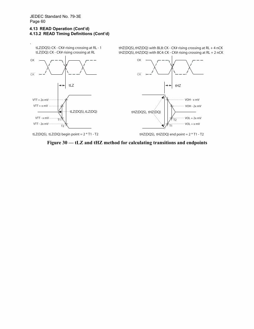
JEDEC Standard No. 79-3EPage 60
4.13 READ Operation (Cont’d)4.13.2 READ Timing Definitions (Cont’d)
.
Figure 30 — tLZ and tHZ method for calculating transitions and endpoints
tHZ(DQS), tHZ(DQ)
tHZ(DQS), tHZ(DQ) end point = 2 * T1 - T2
VOH - x mV
VTT - x mV
VOL + x mV
VTT + x mV VOH - 2x mV
VTT - 2x mV
VOL + 2x mV
VTT + 2x mV
tLZ(DQS), tLZ(DQ)
tLZ(DQS), tLZ(DQ) begin point = 2 * T1 - T2
T1
T1 T2
T2
tLZ(DQS): CK - CK# rising crossing at RL - 1tLZ(DQ): CK - CK# rising crossing at RL
tHZ(DQS), tHZ(DQ) with BL8: CK - CK# rising crossing at RL + 4 nCKtHZ(DQS), tHZ(DQ) with BC4: CK - CK# rising crossing at RL + 2 nCK
CK
CK
CK
CK
tLZ tHZ
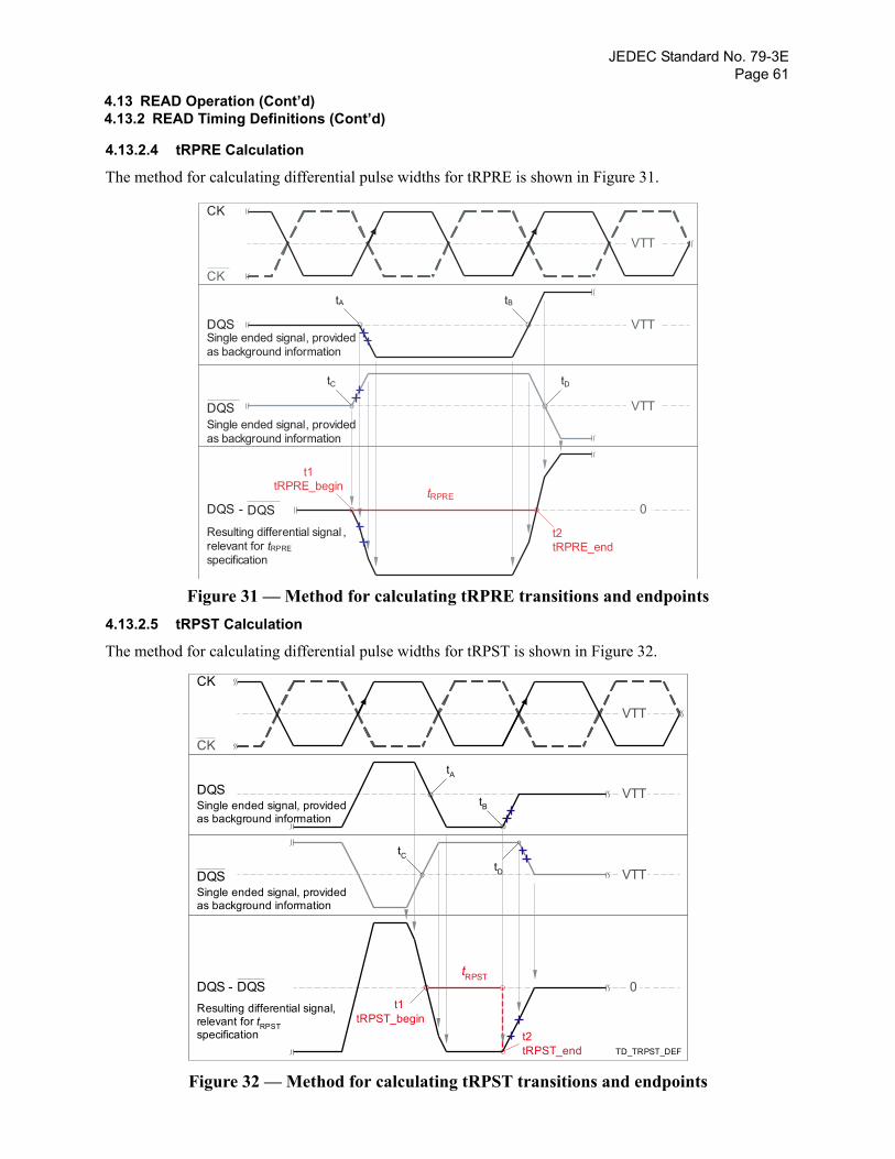
JEDEC Standard No. 79-3EPage 61
4.13 READ Operation (Cont’d)4.13.2 READ Timing Definitions (Cont’d)
4.13.2.4 tRPRE Calculation
The method for calculating differential pulse widths for tRPRE is shown in Figure 31.
Figure 31 — Method for calculating tRPRE transitions and endpoints4.13.2.5 tRPST Calculation
The method for calculating differential pulse widths for tRPST is shown in Figure 32.
Figure 32 — Method for calculating tRPST transitions and endpoints
DQS
DQS
CK
CK
VTT
VTT
0
tC
tA tB
tD
tRPRE
VTT
DQS - DQS
t1tRPRE_begin
t2tRPRE_end
Resulting differential signal ,relevant for tRPRE
specification
Single ended signal, provided as background information
Single ended signal, provided as background information
DQS
DQS
CK
CK
VTT
VTT
0
tC
tA
tB
tD
tRPST
VTT
DQS - DQS t1
tRPST_begint2tRPST_end TD_TRPST_DEF
Resulting differential signal,relevant for tRPSTspecification
Single ended signal, providedas background information
Single ended signal, providedas background information
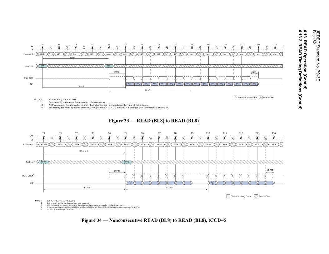
JED
EC
Standard No. 79-3E
Page 62
DON’T CARETRANSITIONING DATA
T12 T13 T14
DOUT
b + 7DOUT
b + 6DOUT
b + 5OUT + 4
tRPST
NOP NOP NOPCOM
DQ
AD
Don’t CareTransitioning Data
T12 T13 T14
DQS
Com NOP NOP NOP
A
tRPST
4.13R
EAD
Operation (C
ont’d)4.13.2
REA
D Tim
ing Definitions (C
ont’d)
Figure 33 — READ (BL8) to READ (BL8)
Figure 34 — Nonconsecutive READ (BL8) to READ (BL8), tCCD=5
NOTE: 1. BL8, RL = 5 (CL = 5, AL = 0) 2. DOUT n (or b) = data-out from column n (or column b). 3. NOP commands are shown for ease of illustration; other commands may be valid at these times. 4. BL8 setting activated by either MR0[A1:0 = 00] or MR0[A1:0 = 01] and A12 = 1 during READ commands at T0 and T4.
DOUT
n + 3DOUT
n + 2DOUT
n + 1DOUT
nRL = 5
RL = 5
T0 T1 T2 T3 T4 T5 T6 T7 T8 T9
tCCD
tRPRE
T10 T11
DOUT
n + 7DOUT
n + 6DOUT
n + 5DOUT n + 4
Bank,Col n
Bank,Col b
DOUT
b + 3DOUT
b + 2DOUT
b + 1DOUT
bDb
NOPREAD READNOP NOP NOP NOP NOP NOP NOP NOP NOP
CK
CK#
MAND3
DQ2
S, DQS#
DRESS4
T0 T1 T2 T3 T4 T5 T6 T7 T8 T9 T10 T11
, DQS#
mand NOP NOP NOP NOP NOP NOP NOP NOP NOP READ NOP READ
ddress Bank,Col n
Bank,Col b
CK
CK#
DQ DOn
DOb
TCCD = 5
RL = 5 RL = 5
tRPRE
NOTE: 1. BL8, RL = 5 (CL = 5, AL = 0), tCCD=5 2. DOUT n (or b) = data-out from column n (or column b). 3. NOP commands are shown for ease of illustration; other commands may be valid at these times. 4. BL8 setting activated by either MR0[A1:0 = 00] or MR0[A1:0 = 01] and A12 = 1 during READ commands at T0 and T4. 5. DQS-DQS# is held logic low at T9
3
4
5
2
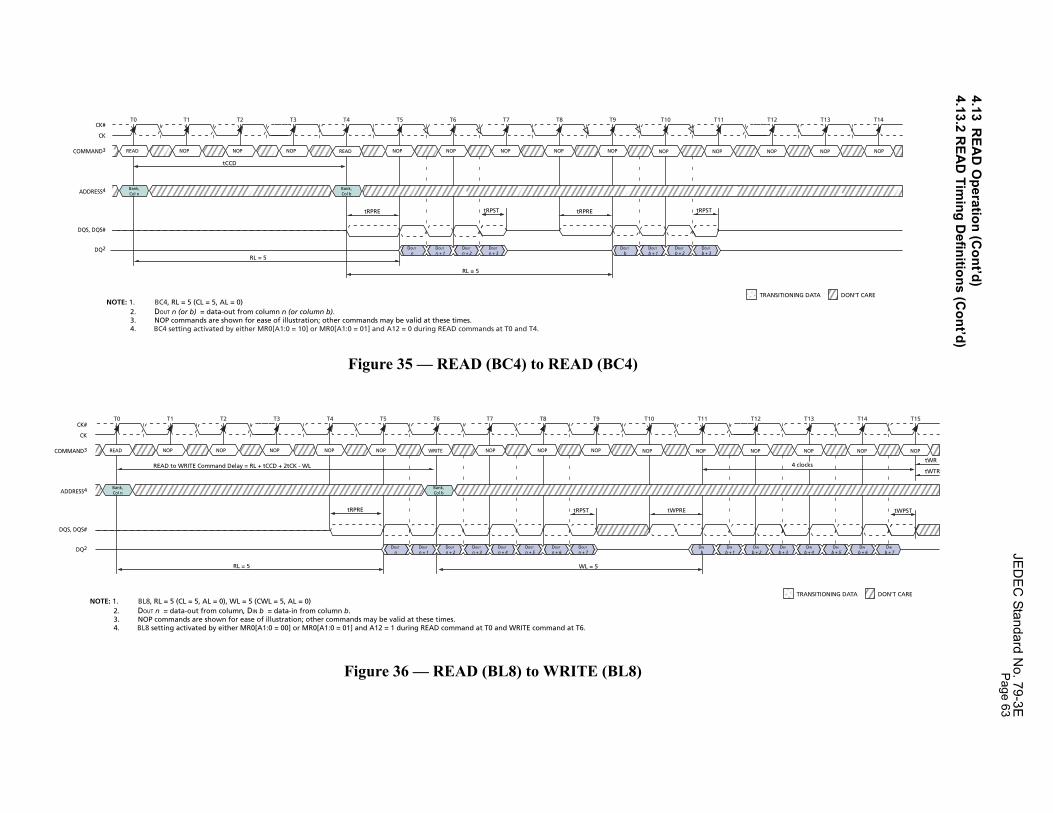
JED
EC
Standard No. 79-3EPage 63
COM
DQ
AD
DON’T CARETRANSITIONING DATA
T12 T13 T14
NOP NOP NOP
DON’T CARETRANSITIONING DATA
T12 T13 T14
DIN
b + 3DIN
b + 2N
1DIN
b + 7DIN
b + 6DIN
b + 5DIN
b + 4
tWPST
NOP NOP NOP
CK
CK
COMMAND
DQ
DQS, DQS
ADDRESS
T15
NOP
tWR
tWTR4 clocks
4.13R
EAD
Operation (C
ont’d)4.13.2 R
EAD
Timing D
efinitions (Cont’d)
Figure 35 — READ (BC4) to READ (BC4)
Figure 36 — READ (BL8) to WRITE (BL8)
NOP
NOTE: 1. BC4, RL = 5 (CL = 5, AL = 0) 2. DOUT n (or b) = data-out from column n (or column b). 3. NOP commands are shown for ease of illustration; other commands may be valid at these times. 4. BC4 setting activated by either MR0[A1:0 = 10] or MR0[A1:0 = 01] and A12 = 0 during READ commands at T0 and T4.
DOUT
n + 3DOUT
n + 2DOUT
n + 1DOUT
n
CK
CK#
MAND3
DQ2
S, DQS#
RL = 5
RL = 5
T0 T1 T2 T3 T4 T5 T6 T7 T8 T9
tCCD
tRPRE
DRESS4
T10 T11
READ READNOP NOP NOP NOP NOP NOP NOP NOP NOP
Bank,Col n
Bank,Col b
DOUT
b + 3DOUT
b + 2DOUT
b + 1DOUT
b
tRPRE tRPSTtRPST
NOTE: 1. BL8, RL = 5 (CL = 5, AL = 0), WL = 5 (CWL = 5, AL = 0) 2. DOUT n = data-out from column, DIN b = data-in from column b. 3. NOP commands are shown for ease of illustration; other commands may be valid at these times. 4. BL8 setting activated by either MR0[A1:0 = 00] or MR0[A1:0 = 01] and A12 = 1 during READ command at T0 and WRITE command at T6.
DOUT
n + 3DOUT
n + 2DOUT
n + 1DOUT
n
RL = 5 WL = 5
T0 T1 T2 T3 T4 T5 T6 T7 T8 T9
tRPRE
T10 T11
DOUT
n + 7DOUT
n + 6DOUT
n + 5DOUT n + 4
Bank,Col n
Bank,Col b
DI
b +DIN
b
tWPREtRPST
NOPREAD WRITENOP NOP NOP NOPNOP NOP NOP NOP NOP
#
3
2
#
4
READ to WRITE Command Delay = RL + tCCD + 2tCK - WL

JED
EC
Standard No. 79-3E
Page 64
DON’T CARETRANSITIONING DATA
T12 T13 T14
NOP NOP NOP
C
CK
COMMAND
DQ
DQS, DQ
ADDRES
T15
NOP
tWR
tWTR
DON’T CARETRANSITIONING DATA
T12 T13 T14
NOP NOP NOPCOM
DQ
AD
4.13R
EAD
Operation (C
ont’d)4.13.2
REA
D Tim
ing Definitions (C
ont’d)
Figure 37 — READ (BC4) to WRITE (BC4) OTF
Figure 38 — READ (BL8) to READ (BC4) OTF
NOTE: 1. BC4, RL = 5 (CL = 5, AL = 0), WL = 5 (CWL = 5, AL = 0) 2. DOUT n = data-out from column, DIN b = data-in from column b. 3. NOP commands are shown for ease of illustration; other commands may be valid at these times. 4. BC4 setting activated by MR0[A1:0 = 01] and A12 = 0 during READ command at T0 and WRITE command at T4.
DOUT
n + 3DOUT
n + 2DOUT
n + 1DOUT
n
RL = 5 WL = 5
T0 T1 T2 T3 T4 T5 T6 T7 T8 T9
tRPRE
T10 T11
Bank,Col n
Bank,Col b
DIN
b + 3DIN
b + 2DIN
b + 1DIN
b
tWPRE tWPSTtRPST
NOPREAD WRITENOP NOP NOPNOPNOP NOP NOP NOP NOP
K
#
3
2
S#
S4
READ to WRITE Command Delay = RL + tCCD / 2 + 2tCK - WL 4 clocks
NOTE: 1. RL = 5 (CL = 5, AL = 0) 2. DOUT n (or b) = data-out from column n (or column b). 3. NOP commands are shown for ease of illustration; other commands may be valid at these times. 4. BL8 setting activated by MR0[A1:0 = 01] and A12 = 1 during READ command at T0. BC4 setting activated by MR0[A1:0 = 01] and A12 = 0 during READ command at T4.
DOUT
n + 3DOUT
n + 2DOUT
n + 1DOUT
nRL = 5
RL = 5
T0 T1 T2 T3 T4 T5 T6 T7 T8 T9
tCCD
tRPRE
T10 T11
DOUT
n + 7DOUT
n + 6DOUT
n + 5DOUT n + 4
Bank,Col n
Bank,Col b
DOUT
b + 3DOUT
b + 2DOUT
b + 1DOUT
b
tRPST
NOPREAD READNOP NOP NOP NOP NOP NOP NOP NOP NOP
CK
CK#
MAND3
DQ2
S, DQS#
DRESS4
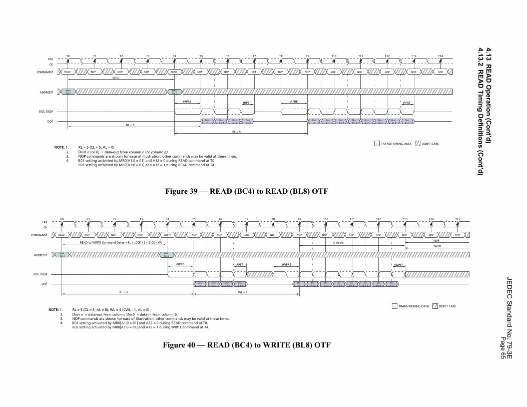
JED
EC
Standard No. 79-3EPage 65
DON’T CARETRANSITIONING DATA
T12 T13 T14
tRPST
NOP NOP NOPCOM
DQ
AD
DOUT
b+ 7DOUT
b+ 6DOUT
b+ 5OUT + 4
DON’T CARETRANSITIONING DATA
T12 T13 T14
DIN
b + 7DIN
b + 6N
5
tWPST
NOP NOP NOPCOMMAN
D
DQS, D
ADDRE
T15
NOP
tWR
tWTR
4.13R
EAD
Operation (C
ont’d)4.13.2
REA
D Tim
ing Definitions (C
ont’d)
Figure 39 — READ (BC4) to READ (BL8) OTF
Figure 40 — READ (BC4) to WRITE (BL8) OTF
NOTE: 1. RL = 5 (CL = 5, AL = 0) 2. DOUT n (or b) = data-out from column n (or column b). 3. NOP commands are shown for ease of illustration; other commands may be valid at these times. 4. BC4 setting activated by MR0[A1:0 = 01] and A12 = 0 during READ command at T0. BL8 setting activated by MR0[A1:0 = 01] and A12 = 1 during READ command at T4.
DOUT
n + 3DOUT
n + 2DOUT
n + 1DOUT
nRL = 5
RL = 5
T0 T1 T2 T3 T4 T5 T6 T7 T8 T9
tCCD
tRPRE
T10 T11
Bank,Col n
Bank,Col b
DOUT
b + 3DOUT
b + 2DOUT
b + 1DOUT
b
tRPST
NOPREAD READNOP NOP NOP NOP NOP NOP NOP NOP NOP
CK
CK#
MAND3
DQ2
S, DQS#
DRESS4
Db
tRPRE
NOTE: 1. RL = 5 (CL = 5, AL = 0), WL = 5 (CWL - 1, AL = 0) 2. DOUT n = data-out from column, DIN b = data-in from column b. 3. NOP commands are shown for ease of illustration; other commands may be valid at these times. 4. BC4 setting activated by MR0[A1:0 = 01] and A12 = 0 during READ command at T0. BL8 setting activated by MR0[A1:0 = 01] and A12 = 1 during WRITE command at T4.
DOUT
n + 3DOUT
n + 2DOUT
n + 1DOUT
n
RL = 5 WL = 5
T0 T1 T2 T3 T4 T5 T6 T7 T8 T9
tRPRE
T10 T11
Bank,Col n
Bank,Col b
DIN
b + 3DIN
b + 2DIN
b + 1DIN
bDI
b +DIN
b + 4
tWPREtRPST
NOPREAD WRITENOP NOP NOPNOPNOP NOP NOP NOP NOP
CK
CK#
D3
Q2
QS#
SS4
READ to WRITE Command Delay = RL + tCCD / 2 + 2tCK - WL 4 clocks
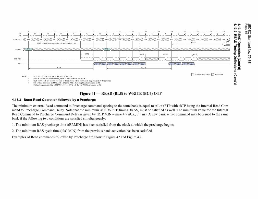
JED
EC
Standard No. 79-3E
Page 66
4.13.3
The m RTP being the Internal Read Com-mand e minimum value for the Internal Read C mmand may be issued to the same bank i
1. The
2. The
Examp
DON’T CARETRANSITIONING DATA
T12 T13 T14
DIN
b + 3DIN
b + 21
tWPST
NOP NOP NOP
CK
CK#
COMMAND3
DQ2
DQS, DQS#
ADDRESS4
T15
NOP
tWR
tWTR 4 clocks
4.13R
EAD
Operation (C
ont’d)4.13.2
REA
D Tim
ing Definitions (C
ont’d
Figure 41 — READ (BL8) to WRITE (BC4) OTFBurst Read Operation followed by a Precharge
inimum external Read command to Precharge command spacing to the same bank is equal to AL + tRTP with tto Precharge Command Delay. Note that the minimum ACT to PRE timing, tRAS, must be satisfied as well. Thommand to Precharge Command Delay is given by tRTP.MIN = max(4 × nCK, 7.5 ns). A new bank active co
f the following two conditions are satisfied simultaneously:
minimum RAS precharge time (tRP.MIN) has been satisfied from the clock at which the precharge begins.
minimum RAS cycle time (tRC.MIN) from the previous bank activation has been satisfied.
les of Read commands followed by Precharge are show in Figure 42 and Figure 43.
NOTE: 1. RL = 5 (CL = 5, AL = 0), WL = 5 (CWL= 5, AL = 0) 2. DOUT n = data-out from column, DIN b = data-in from column b. 3. NOP commands are shown for ease of illustration; other commands may be valid at these times. 4. BL8 setting activated by MR0[A1:0 = 01] and A12 = 1 during READ command at T0. BC4 setting activated by MR0[A1:0 = 01] and A12 = 0 during WRITE command at T6.
DOUT
n + 3DOUT
n + 2DOUT
n + 1DOUT
n
RL = 5 WL = 5
T0 T1 T2 T3 T4 T5 T6 T7 T8 T9
tRPRE
T10 T11
DOUT
n + 7DOUT
n + 6DOUT
n + 5DOUT n + 4
Bank,Col n
Bank,Col b
DIN
b + DIN
b
tWPREtRPST
NOPREAD WRITENOP NOP NOP NOPNOP NOP NOP NOP NOP
READ to WRITE Command Delay = RL + tCCD + 2tCK - WL
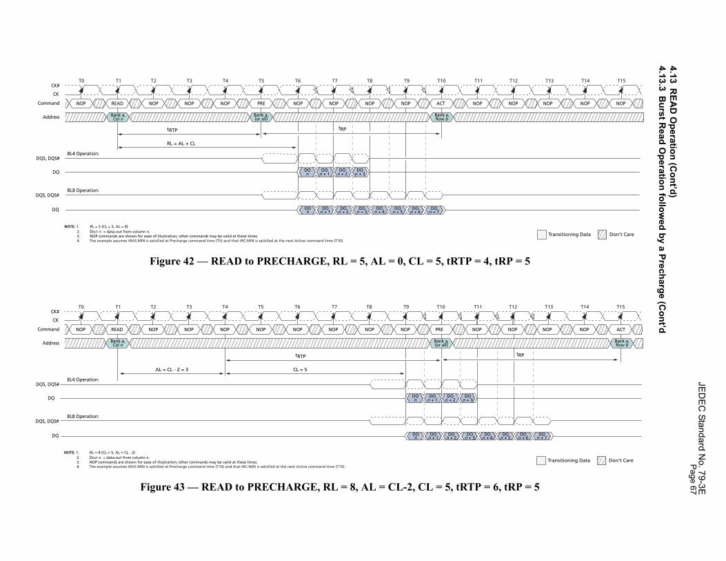
JED
EC
Standard No. 79-3EPage 67
P = 5
tRP = 5
CK
CK#
Don’t CareTransitioning Data
T12 T13 T14 T15
Command NOPNOP NOP NOP
Addres
DQS, DQS#
DQ
DQ
DQS, DQS#
CK
CK#
Don’t CareTransitioning Data
T12 T13 T14 T15
Command NOPNOP ACTNOP
Address Bank a,Row b
tRP
DQS, DQS#
DQ
DQ
DQS, DQS#
O+ 5
DOn + 6
DOn + 7
4.13R
EAD
Operation (C
ont’d)4.13.3
Burst R
ead Operation follow
ed by a Precharge (Cont’d
Figure 42 — READ to PRECHARGE, RL = 5, AL = 0, CL = 5, tRTP = 4, tR
Figure 43 — READ to PRECHARGE, RL = 8, AL = CL-2, CL = 5, tRTP = 6,
T0 T1 T2 T3 T4 T5 T6 T7 T8 T9 T10 T11
NOP NOP NOP NOP NOP NOP NOPACTNOPREAD NOP PRE
s Bank a,Col n
Bank a,(or all)
Bank a,Row b
tRPtRTP
RL = AL + CL
BL4 Operation:
BL8 Operation:
DOn
DOn + 1
DOn + 2
DOn + 3
DOn
DOn + 1
DOn + 2
DOn + 3
DOn + 4
DOn + 5
DOn + 6
DOn + 7
NOTE: 1. RL = 5 (CL = 5, AL = 0) 2. DOUT n = data-out from column n. 3. NOP commands are shown for ease of illustration; other commands may be valid at these times. 4. The example assumes tRAS.MIN is satisfied at Precharge command time (T5) and that tRC.MIN is satisfied at the next Active command time (T10).
T0 T1 T2 T3 T4 T5 T6 T7 T8 T9 T10 T11
NOP NOP NOP NOPNOP NOP NOPNOPNOPREAD NOP PRE
Bank a,Col n
Bank a,(or all)
tRTP
CL = 5AL = CL - 2 = 3
BL4 Operation:
BL8 Operation:
DOn
DOn + 1
DOn + 2
DOn + 3
DOn
DOn + 1
DOn + 2
DOn + 3
DOn + 4
Dn
NOTE: 1. RL = 8 (CL = 5, AL = CL - 2) 2. DOUT n = data-out from column n. 3. NOP commands are shown for ease of illustration; other commands may be valid at these times. 4. The example assumes tRAS.MIN is satisfied at Precharge command time (T10) and that tRC.MIN is satisfied at the next Active command time (T15).

JEDEC Standard No. 79-3EPage 68
4 DDR3 SDRAM Command Description and Operation (Cont’d)
4.14 WRITE Operation4.14.1 DDR3 Burst Operation
During a READ or WRITE command, DDR3 will support BC4 and BL8 on the fly using address A12 dur-ing the READ or WRITE (AUTO PRECHARGE can be enabled or disabled).
A12 = 0, BC4 (BC4 = burst chop, tCCD = 4)
A12 = 1, BL8
A12 is used only for burst length control, not as a column address.
4.14.2 WRITE Timing Violations
4.14.2.1 Motivation
Generally, if timing parameters are violated, a complete reset/initialization procedure has to be initiated to make sure that the DRAM works properly. However, it is desirable, for certain minor violations, that the DRAM is guaranteed not to “hang up,” and that errors are limited to that particular operation.
For the following, it will be assumed that there are no timing violations with regards to the Write command itself (including ODT, etc.) and that it does satisfy all timing requirements not mentioned below.
4.14.2.2 Data Setup and Hold Violations
Should the data to strobe timing requirements (tDS, tDH) be violated, for any of the strobe edges associ-ated with a write burst, then wrong data might be written to the memory location addressed with this WRITE command.
In the example (Figure 44 on page 69), the relevant strobe edges for write burst A are associated with the clock edges: T5, T5.5, T6, T6.5, T7, T7.5, T8, T8.5.
Subsequent reads from that location might result in unpredictable read data, however the DRAM will work properly otherwise.
4.14.2.3 Strobe to Strobe and Strobe to Clock Violations
Should the strobe timing requirements (tDQSH, tDQSL, tWPRE, tWPST) or the strobe to clock timing requirements (tDSS, tDSH, tDQSS) be violated, for any of the strobe edges associated with a Write burst, then wrong data might be written to the memory location addressed with the offending WRITE command. Subsequent reads from that location might result in unpredictable read data, however the DRAM will work properly otherwise.
In the example (Figure 52 on page 73) the relevant strobe edges for Write burst n are associated with the clock edges: T4, T4.5, T5, T5.5, T6, T6.5, T7, T7.5, T8, T8.5 and T9. Any timing requirements starting or ending on one of these strobe edges need to be fulfilled for a valid burst. For Write burst b the relevant edges are T8, T8.5, T9, T9.5, T10, T10.5, T11, T11.5, T12, T12.5 and T13. Some edges are associated with both bursts.
4.14.2.4 Write Timing Parameters
This drawing is for example only to enumerate the strobe edges that “belong” to a Write burst. No actual timing violations are shown here. For a valid burst all timing parameters for each edge of a burst need to be satisfied (not only for one edge - as shown).
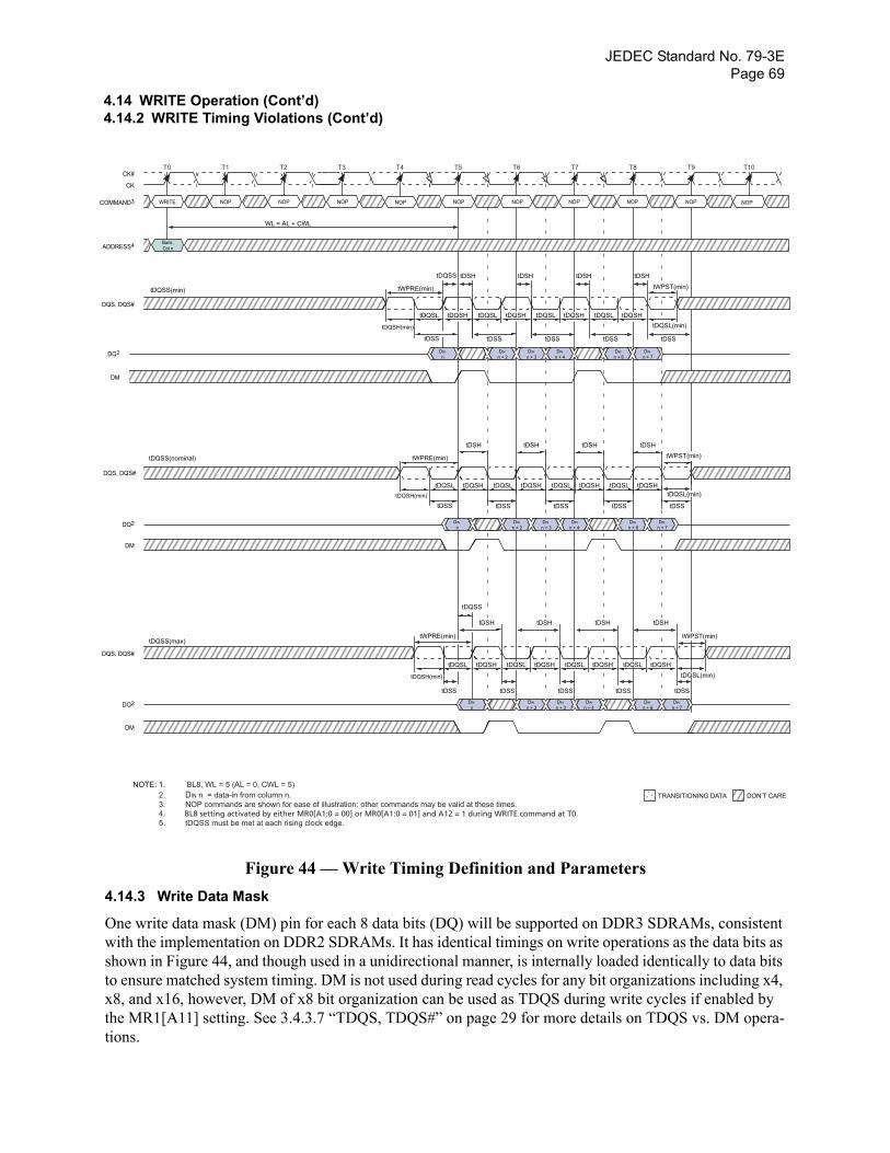
JEDEC Standard No. 79-3EPage 69
4.14 WRITE Operation (Cont’d)4.14.2 WRITE Timing Violations (Cont’d)
Figure 44 — Write Timing Definition and Parameters4.14.3 Write Data Mask
One write data mask (DM) pin for each 8 data bits (DQ) will be supported on DDR3 SDRAMs, consistent with the implementation on DDR2 SDRAMs. It has identical timings on write operations as the data bits as shown in Figure 44, and though used in a unidirectional manner, is internally loaded identically to data bits to ensure matched system timing. DM is not used during read cycles for any bit organizations including x4, x8, and x16, however, DM of x8 bit organization can be used as TDQS during write cycles if enabled by the MR1[A11] setting. See 3.4.3.7 “TDQS, TDQS#” on page 29 for more details on TDQS vs. DM opera-tions.
NOTE: 1. BL8, WL = 5 (AL = 0, CWL = 5) 2. DIN n = data-in from column n. 3. NOP commands are shown for ease of illustration; other commands may be valid at these times. 4. BL8 setting activated by either MR0[A1:0 = 00] or MR0[A1:0 = 01] and A12 = 1 during WRITE command at T0. 5. tDQSS must be met at each rising clock edge.
DIN
n + 3DIN
n + 2DIN
n + 1DIN
n
WL = AL + CWL
T0 T1 T2 T3 T4 T5 T6 T7 T8 T9 T10
DON’T CARETRANSITIONING DATA
DIN
n + 7DIN
n + 6DIN
n + 5DIN
n + 4
Bank,Col n
NOPWRITE NOPNOP NOP NOP NOP NOP NOP NOP NOP
CK
CK#
COMMAND3
DQ2
DQS, DQS#
ADDRESS4
tWPST(min)
tWPST(min)
tDQSL
tDQSS(min)
DIN
n + 3DIN
n + 2DIN
n + 1DIN
nDIN
n + 7DIN
n + 6DIN
n + 5DIN
n + 4DQ2
DIN
n + 3DIN
n + 2DIN
n + 1DIN
nDIN
n + 7DIN
n + 6DIN
n + 5DIN
n + 4DQ2
DQS, DQS#
DQS, DQS#
tDQSS(max)
tDQSS(nominal)
tDQSL
tWPRE(min)
tDQSL
tDQSS
tDQSS
tDSS tDSS tDSS tDSS tDSS
tDSH tDSH tDSH tDSH
tDSS tDSS tDSS tDSS tDSS
tDSS tDSS tDSS tDSS tDSS
tDSH tDSH tDSH tDSH
tDSH tDSH tDSH tDSH
tDQSLtDQSH tDQSLtDQSH tDQSLtDQSH tDQSH
tDQSLtDQSH tDQSLtDQSH tDQSLtDQSH tDQSH
tDQSLtDQSH tDQSLtDQSH tDQSLtDQSH tDQSH
tWPRE(min)
tWPRE(min)
tDQSH(min)
tDQSH(min)
tDQSH(min)
tWPST(min)
tDQSL(min)
tDQSL(min)
tDQSL(min)
DM
DM
DM

JEDEC Standard No. 79-3EPage 70
4 DDR3 SDRAM Command Description and Operation (Cont’d)4.14 WRITE Operation (Cont’d)
4.14.4 tWPRE Calculation
The method for calculating differential pulse widths for tWPRE is shown in Figure 45.
Figure 45 — Method for calculating tWPRE transitions and endpoints
4.14.5 tWPST Calculation
The method for calculating differential pulse widths for tWPST is shown in Figure 46.
Figure 46 — Method for calculating tWPST transitions and endpoints
CK
CK
VTT
DQS - DQS
t1tWPRE_begin
t2tWPRE
tWPRE
_endResulting differential signal
,
relevant for tWPRE
specification
0 V
CK
CK
tWPST
VTT
DQS - DQS t1
tWPST_begint2tWPST_end
Resulting differential signal,relevant for tWPSTspecification
0 V
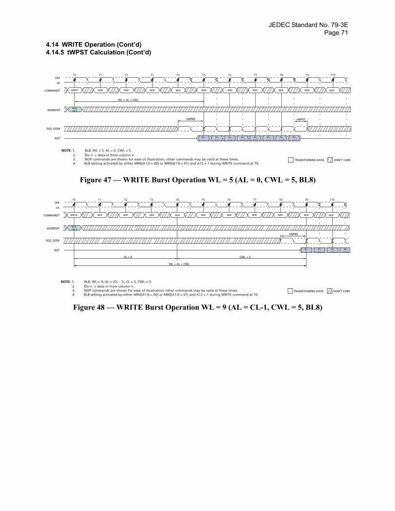
JEDEC Standard No. 79-3EPage 71
4.14 WRITE Operation (Cont’d)4.14.5 tWPST Calculation (Cont’d)
Figure 47 — WRITE Burst Operation WL = 5 (AL = 0, CWL = 5, BL8)
Figure 48 — WRITE Burst Operation WL = 9 (AL = CL-1, CWL = 5, BL8)
NOTE: 1. BL8, WL = 5; AL = 0, CWL = 5. 2. DIN n = data-in from column n. 3. NOP commands are shown for ease of illustration; other commands may be valid at these times. 4. BL8 setting activated by either MR0[A1:0 = 00] or MR0[A1:0 = 01] and A12 = 1 during WRITE command at T0.
DIN
n + 3DIN
n + 2DIN
n + 1DIN
n
WL = AL + CWL
T0 T1 T2 T3 T4 T5 T6 T7 T8 T9
tWPRE
T10
DON’T CARETRANSITIONING DATA
DIN
n + 7DIN
n + 6DIN
n + 5DIN
n + 4
Bank,Col n
NOPWRITE NOPNOP NOP NOP NOP NOP NOP NOP NOP
CK
CK#
COMMAND3
DQ2
DQS, DQS#
ADDRESS4
tWPST
NOTE: 1. BL8, WL = 9; AL = (CL - 1), CL = 5, CWL = 5. 2. DIN n = data-in from column n. 3. NOP commands are shown for ease of illustration; other commands may be valid at these times. 4. BL8 setting activated by either MR0[A1:0 = 00] or MR0[A1:0 = 01] and A12 = 1 during WRITE command at T0.
DIN
n + 3DIN
n + 2DIN
n + 1DIN
n
T0 T1 T2 T3 T4 T5 T6 T7 T8 T9
tWPRE
T10
DON’T CARETRANSITIONING DATA
Bank,Col n
NOPWRITE NOPNOP NOP NOP NOP NOP NOP NOP NOP
CK
CK#
COMMAND3
DQ2
DQS, DQS#
ADDRESS4
WL = AL + CWL
AL = 4 CWL = 5

JEDEC Standard No. 79-3EPage 72
COMMA
DQS, D
ADDR
Care
4.14 WRITE Operation (Cont’d)4.14.5 tWPST Calculation (Cont’d)
Figure 49 — WRITE (BC4) to READ (BC4) Operation
Figure 50 — WRITE (BC4) to PRECHARGE Operation
Figure 51 — WRITE (BC4) OTF to PRECHARGE Operation
NOTE: 1. BC4, WL = 5, RL = 5. 2. DIN n = data-in from column n; DOUT b = data-out from column b. 3. NOP commands are shown for ease of illustration; other commands may be valid at these times. 4. BC4 setting activated by MR0[A1:0 = 10] during WRITE command at T0 and READ command at Tn. 5. tWTR controls the write to read delay to the same device and starts with the first rising clock edge after the last write data shown at T7.
DIN
n + 3DIN
n + 2DIN
n + 1DIN
n
WL = 5 RL = 5
T0 T1 T2 T3 T4 T5 T6 T7 T8 T9 Tn
DON’T CARETRANSITIONING DATA
Bank,Col n
Bank,Col b
NOPWRITE READNOP NOP NOP NOP NOP NOP NOPNOP
CK
CK#
COMMAND3
DQ2
DQS, DQS#
ADDRESS4
tWPST
tWTR5
tWPRE
NOTE: 1. BC4, WL = 5, RL = 5. 2. DIN n = data-in from column n; DOUT b = data-out from column b. 3. NOP commands are shown for ease of illustration; other commands may be valid at these times. 4. BC4 setting activated by MR0[A1:0 = 10] during WRITE command at T0. 5. The write recovery time (tWR) referenced from the first rising clock edge after the last write data shown at T7. tWR specifies the last burst write cycle until the precharge command can be issued to the same bank .
DIN
n + 3DIN
n + 2DIN
n + 1DIN
n
WL = 5
T0 T1 T2 T3 T4 T5 T6 T7 T8 T9 Tn
DON’T CARETRANSITIONING DATA
Bank,Col n
NOPWRITE PRENOP NOP NOP NOP NOP NOP NOPNOP
CK
CK#
COMMAND3
DQ2
DQS, DQS#
ADDRESS4
tWPST
tWR5
tWPRE
NOTE: 1. BC4 OTF, WL = 5 (CWL = 5, AL = 0) 2. DIN n (or b) = data-in from column n. 3. NOP commands are shown for ease of illustration; other commands may be valid at these times. 4. BC4 OTF setting activated by MR0[A1:0 = 01] and A12 = 0 during WRITE command at T0. 5. The write recovery time (tWR) starts at the rising clock edge T9 (4 clocks from T5).
DIN
n + 3DIN
n + 2DIN
n + 1DIN
n
WL = 5
T0 T1 T2 T3 T4 T5 T6 T7 T8 T9
tWPRE
T10 T11 Ta0 Ta1 T14
Bank,Col n VALID
NOPWRITE NOPNOP NOP NOP NOP NOP NOP NOP NOP NOP NOP NOP
CK
CK#
ND3
DQ2
QS#
ESS4
tWPST
4 clocks
PRE
tWR5
Don’t ()()
()()
Time Break
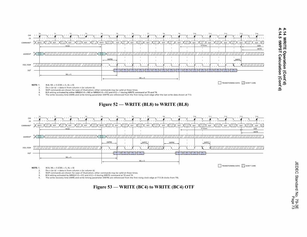
JED
EC
Standard No. 79-3EPage 73
DON’T CARETRANSITIONING DATA
T12 T13 T14
DIN
b + 7DIN
b + 6DIN
b + 5
NOP NOP NOPCOM
DQ
AD
tWPST
tWR
tWTR
DON’T CARETRANSITIONING DATA
T12 T13 T14
NOP NOP NOPCOM
DQ
AD
tWR
tWTR
4.14W
RITE O
peration (Cont’d)
4.14.5tW
PST Calculation (C
ont’d)
Figure 52 — WRITE (BL8) to WRITE (BL8)
Figure 53 — WRITE (BC4) to WRITE (BC4) OTF
NOTE: 1. BL8, WL = 5 (CWL = 5, AL = 0) 2. DIN n (or b) = data-in from column n (or column b). 3. NOP commands are shown for ease of illustration; other commands may be valid at these times. 4. BL8 setting activated by either MR0[A1:0 = 00] or MR0[A1:0 = 01] and A12 = 1 during WRITE command at T0 and T4. 5. The write recovery time (tWR) and write timing parameter (tWTR) are referenced from the first rising clock edge after the last write data shown at T13.
DIN
n + 3DIN
n + 2DIN
n + 1DIN
n
WL = 5
WL = 5
T0 T1 T2 T3 T4 T5 T6 T7 T8 T9
tCCD
tWPRE
T10 T11
DIN
n + 7DIN
n + 6DIN
n + 5DIN
n + 4
Bank,Col n
Bank,Col b
DIN
b + 3DIN
b + 2DIN
b + 1DIN
bDIN
b + 4
NOPWRITE WRITENOP NOP NOP NOP NOP NOP NOP NOP NOP
CK
CK#
MAND3
DQ2
S, DQS#
DRESS4
4 clocks
NOTE: 1. BC4, WL = 5 (CWL = 5, AL = 0) 2. DIN n (or b) = data-in from column n (or column b). 3. NOP commands are shown for ease of illustration; other commands may be valid at these times. 4. BC4 setting activated by MR0[A1:0 = 01] and A12 = 0 during WRITE command at T0 and T4. 5. The write recovery time (tWR) and write timing parameter (tWTR) are referenced from the first rising clock edge at T13 (4 clocks from T9).
DIN
n + 3DIN
n + 2DIN
n + 1DIN
n
WL = 5
WL = 5
T0 T1 T2 T3 T4 T5 T6 T7 T8 T9
tCCD
tWPRE
T10 T11
Bank,Col n
Bank,Col b
DIN
b + 3DIN
b + 2DIN
b + 1DIN
b
NOPWRITE WRITENOP NOP NOP NOP NOP NOP NOP NOP NOP
CK
CK#
MAND3
DQ2
S, DQS#
DRESS4
tWPSTtWPST tWPRE
4 clocks
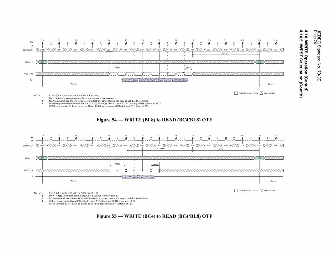
JED
EC
Standard No. 79-3E
Page 74
RL = 5
DON’T CARETRANSITIONING DATA
T12 T13 T14
Bank,Col b
READNOP NOPCOM
DQ
AD
RL = 5
DON’T CARETRANSITIONING DATA
T12 T13 T14
Bank,Col b
READNOP NOPCOM
DQ
AD
4.14W
RITE O
peration (Cont’d)
4.14.5tW
PST Calculation (C
ont’d)
Figure 54 — WRITE (BL8) to READ (BC4/BL8) OTF
Figure 55 — WRITE (BC4) to READ (BC4/BL8) OTF
NOTE: 1. RL = 5 (CL = 5, AL = 0), WL = 5 (CWL = 5, AL = 0) 2. DIN n = data-in from column n; DOUT b = data-out from column b. 3. NOP commands are shown for ease of illustration; other commands may be valid at these times. 4. BL8 setting activated by either MR0[A1:0 = 00] or MR0[A1:0 = 01] and A12 = 1 during WRITE command at T0. READ command at T13 can be either BC4 or BL8 depending on MR0[A1:0] and A12 status at T13.
DIN
n + 3DIN
n + 2DIN
n + 1DIN
n
WL = 5
T0 T1 T2 T3 T4 T5 T6 T7 T8 T9
tWPRE
T10 T11
DIN
n + 7DIN
n + 6DIN
n + 5DIN
n + 4
Bank,Col n
NOPWRITE NOP NOP NOP NOP NOP NOP NOP NOPNOP NOP
CK
CK#
MAND3
DQ2
S, DQS#
DRESS4
tWPST
tWTR
NOTE: 1. RL = 5 (CL = 5, AL = 0), WL = 5 (CWL =5, AL = 0) 2. DIN n = data-in from column n; DOUT b = data-out from column b. 3. NOP commands are shown for ease of illustration; other commands may be valid at these times. 4. BC4 setting activated by MR0[A1:0 = 01] and A12 = 0 during WRITE command at T0. READ command at T13 can be either BC4 or BL8 depending on A12 status at T13.
DIN
n + 3DIN
n + 2DIN
n + 1DIN
n
WL = 5
T0 T1 T2 T3 T4 T5 T6 T7 T8 T9
tWPRE
T10 T11
Bank,Col n
NOPWRITE NOP NOP NOP NOP NOP NOP NOP NOPNOP NOP
CK
CK#
MAND3
DQ2
S, DQS#
DRESS4
tWPST
tWTR 4 clocks
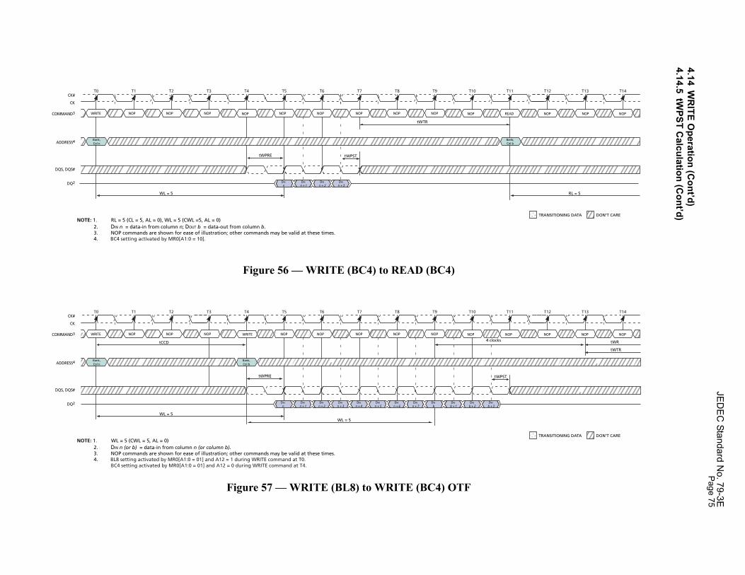
JED
EC
Standard No. 79-3EPage 75
RL = 5
DON’T CARETRANSITIONING DATA
T12 T13 T14
NOP NOP NOPCOM
DQ
AD
DON’T CARETRANSITIONING DATA
T12 T13 T14
NOP NOP NOPCOM
DQ
AD
tWR
tWTR
4.14W
RITE O
peration (Cont’d)
4.14.5tW
PST Calculation (C
ont’d)
Figure 56 — WRITE (BC4) to READ (BC4)
Figure 57 — WRITE (BL8) to WRITE (BC4) OTF
NOTE: 1. RL = 5 (CL = 5, AL = 0), WL = 5 (CWL =5, AL = 0) 2. DIN n = data-in from column n; DOUT b = data-out from column b. 3. NOP commands are shown for ease of illustration; other commands may be valid at these times. 4. BC4 setting activated by MR0[A1:0 = 10].
DIN
n + 3DIN
n + 2DIN
n + 1DIN
n
WL = 5
T0 T1 T2 T3 T4 T5 T6 T7 T8 T9
tWPRE
T10 T11
Bank,Col n
Bank,Col b
NOPWRITE READNOP NOP NOP NOP NOP NOP NOP NOPNOP
CK
CK#
MAND3
DQ2
S, DQS#
DRESS4
tWPST
tWTR
NOTE: 1. WL = 5 (CWL = 5, AL = 0) 2. DIN n (or b) = data-in from column n (or column b). 3. NOP commands are shown for ease of illustration; other commands may be valid at these times. 4. BL8 setting activated by MR0[A1:0 = 01] and A12 = 1 during WRITE command at T0. BC4 setting activated by MR0[A1:0 = 01] and A12 = 0 during WRITE command at T4.
DIN
n + 3DIN
n + 2DIN
n + 1DIN
n
WL = 5WL = 5
T0 T1 T2 T3 T4 T5 T6 T7 T8 T9
tCCD
tWPRE
T10 T11
DIN
n + 7DIN
n + 6DIN
n + 5DIN
n + 4
Bank,Col n
Bank,Col b
DIN
b + 3DIN
b + 2DIN
b + 1DIN
b
NOPWRITE WRITENOP NOP NOP NOP NOP NOP NOP NOP NOP
CK
CK#
MAND3
DQ2
S, DQS#
DRESS4
tWPST
4 clocks
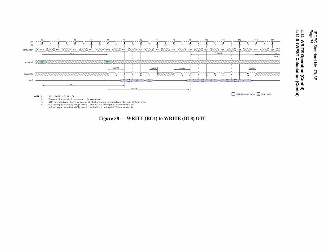
JED
EC
Standard No. 79-3E
Page 76
DON’T CARETRANSITIONING DATA
T12 T13 T14
DIN
b + 7DIN
b + 6DIN
b + 5
NOP NOP NOPCOM
DQ
AD
tWPST
tWR
tWTR
4.14W
RITE O
peration (Cont’d)
4.14.5tW
PST Calculation (C
ont’d)
Figure 58 — WRITE (BC4) to WRITE (BL8) OTF
NOTE: 1. WL = 5 (CWL = 5, AL = 0) 2. DIN n (or b) = data-in from column n (or column b). 3. NOP commands are shown for ease of illustration; other commands may be valid at these times. 4. BC4 setting activated by MR0[A1:0 = 01] and A12 = 0 during WRITE command at T0. BL8 setting activated by MR0[A1:0 = 01] and A12 = 1 during WRITE command at T4.
DIN
n + 3DIN
n + 2DIN
n + 1DIN
n
WL = 5
WL = 5
T0 T1 T2 T3 T4 T5 T6 T7 T8 T9
tCCD
tWPRE
T10 T11
Bank,Col n
Bank,Col b
DIN
b + 3DIN
b + 2DIN
b + 1DIN
bDIN
b + 4
NOPWRITE WRITENOP NOP NOP NOP NOP NOP NOP NOP NOP
CK
CK#
MAND3
DQ2
S, DQS#
DRESS4
tWPST tWPRE
4 clocks
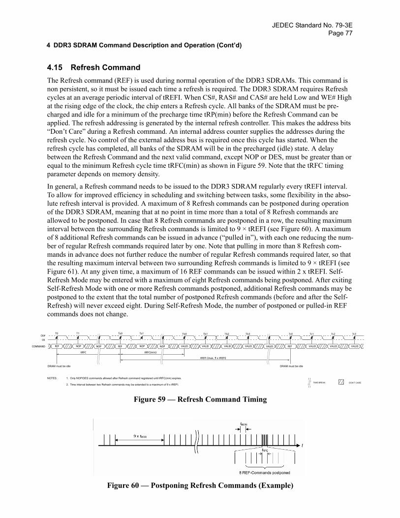
JEDEC Standard No. 79-3EPage 77
C
COMMA
E
4 DDR3 SDRAM Command Description and Operation (Cont’d)
4.15 Refresh CommandThe Refresh command (REF) is used during normal operation of the DDR3 SDRAMs. This command is non persistent, so it must be issued each time a refresh is required. The DDR3 SDRAM requires Refresh cycles at an average periodic interval of tREFI. When CS#, RAS# and CAS# are held Low and WE# High at the rising edge of the clock, the chip enters a Refresh cycle. All banks of the SDRAM must be pre-charged and idle for a minimum of the precharge time tRP(min) before the Refresh Command can be applied. The refresh addressing is generated by the internal refresh controller. This makes the address bits “Don’t Care” during a Refresh command. An internal address counter supplies the addresses during the refresh cycle. No control of the external address bus is required once this cycle has started. When the refresh cycle has completed, all banks of the SDRAM will be in the precharged (idle) state. A delay between the Refresh Command and the next valid command, except NOP or DES, must be greater than or equal to the minimum Refresh cycle time tRFC(min) as shown in Figure 59. Note that the tRFC timing parameter depends on memory density.
In general, a Refresh command needs to be issued to the DDR3 SDRAM regularly every tREFI interval. To allow for improved efficiency in scheduling and switching between tasks, some flexibility in the abso-lute refresh interval is provided. A maximum of 8 Refresh commands can be postponed during operation of the DDR3 SDRAM, meaning that at no point in time more than a total of 8 Refresh commands are allowed to be postponed. In case that 8 Refresh commands are postponed in a row, the resulting maximum interval between the surrounding Refresh commands is limited to 9 × tREFI (see Figure 60). A maximum of 8 additional Refresh commands can be issued in advance (“pulled in”), with each one reducing the num-ber of regular Refresh commands required later by one. Note that pulling in more than 8 Refresh com-mands in advance does not further reduce the number of regular Refresh commands required later, so that the resulting maximum interval between two surrounding Refresh commands is limited to 9 × tREFI (see Figure 61). At any given time, a maximum of 16 REF commands can be issued within 2 x tREFI. Self-Refresh Mode may be entered with a maximum of eight Refresh commands being postponed. After exiting Self-Refresh Mode with one or more Refresh commands postponed, additional Refresh commands may be postponed to the extent that the total number of postponed Refresh commands (before and after the Self-Refresh) will never exceed eight. During Self-Refresh Mode, the number of postponed or pulled-in REF commands does not change.
Figure 59 — Refresh Command Timing
Figure 60 — Postponing Refresh Commands (Example)
NOPREF NOPREF VALID VALID VALID VALID REF VALIDVALIDVALID
CK
K#
ND
tRFC tRFC(min)
tREFI (max. 9 x tREFI)
NOTES: 1. Only NOP/DES commands allowed after Refresh command registered until tRFC(min) expires. 2. Time interval between two Refresh commands may be extended to a maximum of 9 x tREFI.
DON’T CAR
()()
()()
TIME BREAK
T0 T1 Ta0 Ta1 Tb0 Tb1 Tb2 Tb3 Tc0 Tc1 Tc2 Tc3
VALIDNOPNOP
DRAM must be idle DRAM must be idle

JEDEC Standard No. 79-3EPage 78
4 DDR3 SDRAM Command Description and Operation (Cont’d)4.15 Self-Refresh Operation (Cont’d)
Figure 61 — Pulling-in Refresh Commands (Example)
JEDEC Standard No. 79-3EPage 79
4 DDR3 SDRAM Command Description and Operation (Cont’d)
4.16 Self-Refresh OperationThe Self-Refresh command can be used to retain data in the DDR3 SDRAM, even if the rest of the system is powered down. When in the Self-Refresh mode, the DDR3 SDRAM retains data without external clock-ing. The DDR3 SDRAM device has a built-in timer to accommodate Self-Refresh operation. The Self-Refresh-Entry (SRE) Command is defined by having CS#, RAS#, CAS#, and CKE held low with WE# high at the rising edge of the clock.
Before issuing the Self-Refresh-Entry command, the DDR3 SDRAM must be idle with all bank precharge state with tRP satisfied. ‘Idle state’ is defined as all banks are closed (tRP, tDAL, etc. satisfied), no data bursts are in progress, CKE is high, and all timings from previous operations are satisfied (tMRD, tMOD, tRFC, tZQinit, tZQoper, tZQCS, etc.) Also, on-die termination must be turned off before issuing Self-Refresh-Entry com-mand, by either registering ODT pin low “ODTL + 0.5tCK” prior to the Self-Refresh Entry command or using MRS to MR1 command. Once the Self-Refresh Entry command is registered, CKE must be held low to keep the device in Self-Refresh mode. During normal operation (DLL on), MR1 (A0 = 0), the DLL is automatically disabled upon entering Self-Refresh and is automatically enabled (including a DLL-Reset) upon exiting Self-Refresh.
When the DDR3 SDRAM has entered Self-Refresh mode, all of the external control signals, except CKE and RESET#, are “don’t care.” For proper Self-Refresh operation, all power supply and reference pins (VDD, VDDQ, VSS, VSSQ, VRefCA and VRefDQ) must be at valid levels. VrefDQ supply may be turned OFF and VREFDQ may take any value between VSS and VDD during Self Refresh operation, provided that VrefDQ is valid and stable prior to CKE going back High and that first Write operation or first Write Leveling Activity may not occur earlier than 512 nCK after exit from Self Refresh. The DRAM initiates a minimum of one Refresh command internally within tCKE period once it enters Self-Refresh mode.
The clock is internally disabled during Self-Refresh Operation to save power. The minimum time that the DDR3 SDRAM must remain in Self-Refresh mode is tCKESR. The user may change the external clock frequency or halt the external clock tCKSRE after Self-Refresh entry is registered, however, the clock must be restarted and stable tCKSRX before the device can exit Self-Refresh operation.
The procedure for exiting Self-Refresh requires a sequence of events. First, the clock must be stable prior to CKE going back HIGH. Once a Self-Refresh Exit command (SRX, combination of CKE going high and either NOP or Deselect on command bus) is registered, a delay of at least tXS must be satisfied before a valid command not requiring a locked DLL can be issued to the device to allow for any internal refresh in progress. Before a command that requires a locked DLL can be applied, a delay of at least tXSDLL must be satisfied. Depending on the system environment and the amount of time spent in Self-Refresh, ZQ cali-bration commands may be required to compensate for the voltage and temperature drift as described in “ZQ Calibration Commands” on page 107. To issue ZQ calibration commands, applicable timing require-ments must be satisfied (See Figure 90 — “ZQ Calibration Timing” on page 108).
CKE must remain HIGH for the entire Self-Refresh exit period tXSDLL for proper operation except for Self-Refresh re-entry. Upon exit from Self-Refresh, the DDR3 SDRAM can be put back into Self-Refresh mode after waiting at least tXS period and issuing one refresh command (refresh period of tRFC). NOP or deselect commands must be registered on each positive clock edge during the Self-Refresh exit interval tXS. ODT must be turned off during tXSDLL.
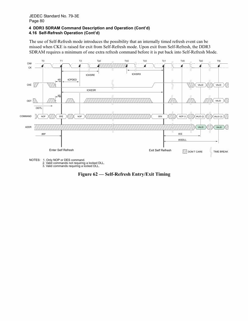
JEDEC Standard No. 79-3EPage 80
COMM
A
EAK
4 DDR3 SDRAM Command Description and Operation (Cont’d)4.16 Self-Refresh Operation (Cont’d)
The use of Self-Refresh mode introduces the possibility that an internally timed refresh event can be missed when CKE is raised for exit from Self-Refresh mode. Upon exit from Self-Refresh, the DDR3 SDRAM requires a minimum of one extra refresh command before it is put back into Self-Refresh Mode.
Figure 62 — Self-Refresh Entry/Exit Timing
CK
CK#
AND NOP NOPSRE
DDR
CKE
ODT
VALID
VALID (2)SRX NOP (1)
tRP tXS
tXSDLL
tCKESR
ODTL
tCPDEDtIS
tCKSRE tCKSRX
tIS
Enter Self Refresh Exit Self Refresh
T0 T1 T2 Tc0 Tc1 Td0Tb0
DON’T CARE
Te0
VALID
VALID (3)
VALID
VALID VALID
TIME BR
Ta0 Tf0
NOTES: 1. Only NOP or DES command. 2. Valid commands not requiring a locked DLL. 3. Valid commands requiring a locked DLL.
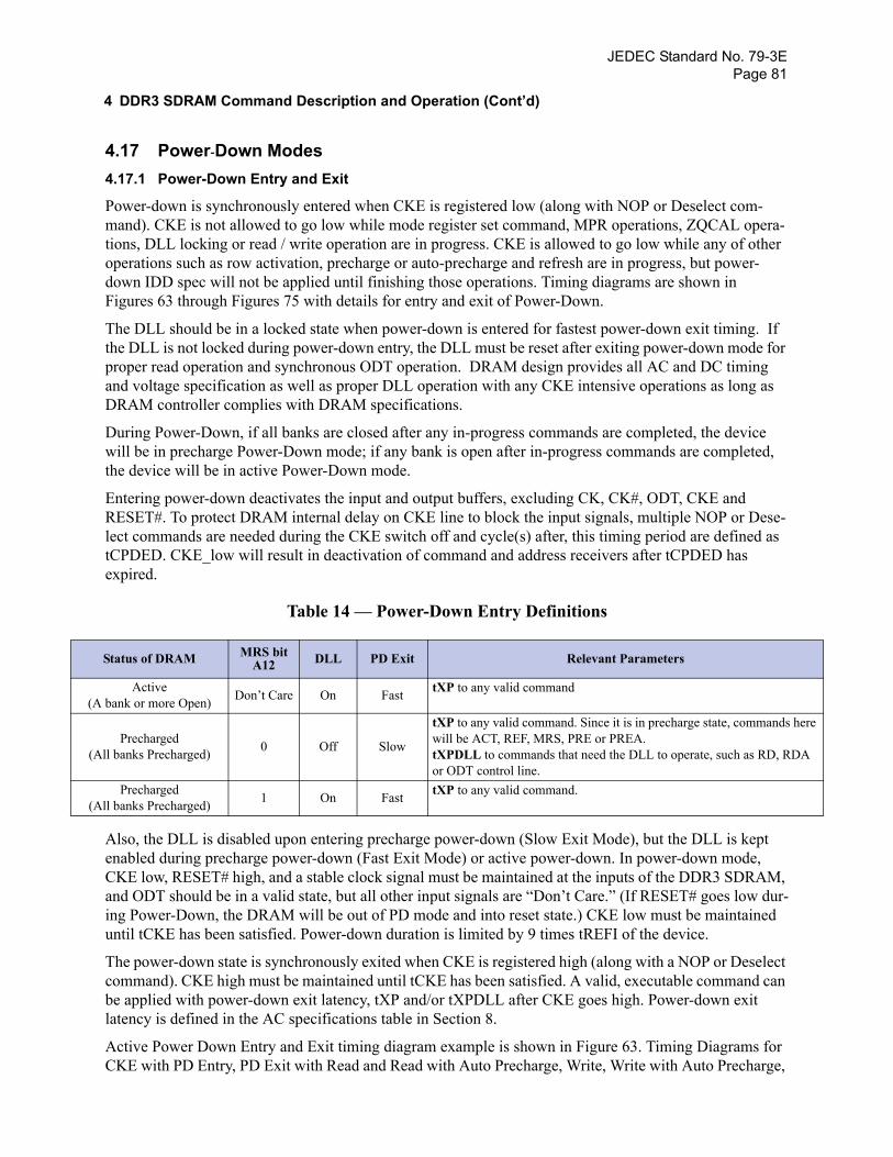
JEDEC Standard No. 79-3EPage 81
(
(
re
(
4 DDR3 SDRAM Command Description and Operation (Cont’d)
4.17 Power-Down Modes 4.17.1 Power-Down Entry and Exit
Power-down is synchronously entered when CKE is registered low (along with NOP or Deselect com-mand). CKE is not allowed to go low while mode register set command, MPR operations, ZQCAL opera-tions, DLL locking or read / write operation are in progress. CKE is allowed to go low while any of other operations such as row activation, precharge or auto-precharge and refresh are in progress, but power-down IDD spec will not be applied until finishing those operations. Timing diagrams are shown in Figures 63 through Figures 75 with details for entry and exit of Power-Down.
The DLL should be in a locked state when power-down is entered for fastest power-down exit timing. If the DLL is not locked during power-down entry, the DLL must be reset after exiting power-down mode for proper read operation and synchronous ODT operation. DRAM design provides all AC and DC timing and voltage specification as well as proper DLL operation with any CKE intensive operations as long as DRAM controller complies with DRAM specifications.
During Power-Down, if all banks are closed after any in-progress commands are completed, the device will be in precharge Power-Down mode; if any bank is open after in-progress commands are completed, the device will be in active Power-Down mode.
Entering power-down deactivates the input and output buffers, excluding CK, CK#, ODT, CKE and RESET#. To protect DRAM internal delay on CKE line to block the input signals, multiple NOP or Dese-lect commands are needed during the CKE switch off and cycle(s) after, this timing period are defined as tCPDED. CKE_low will result in deactivation of command and address receivers after tCPDED has expired.
Table 14 — Power-Down Entry Definitions
Also, the DLL is disabled upon entering precharge power-down (Slow Exit Mode), but the DLL is kept enabled during precharge power-down (Fast Exit Mode) or active power-down. In power-down mode, CKE low, RESET# high, and a stable clock signal must be maintained at the inputs of the DDR3 SDRAM, and ODT should be in a valid state, but all other input signals are “Don’t Care.” (If RESET# goes low dur-ing Power-Down, the DRAM will be out of PD mode and into reset state.) CKE low must be maintained until tCKE has been satisfied. Power-down duration is limited by 9 times tREFI of the device.
The power-down state is synchronously exited when CKE is registered high (along with a NOP or Deselect command). CKE high must be maintained until tCKE has been satisfied. A valid, executable command can be applied with power-down exit latency, tXP and/or tXPDLL after CKE goes high. Power-down exit latency is defined in the AC specifications table in Section 8.
Active Power Down Entry and Exit timing diagram example is shown in Figure 63. Timing Diagrams for CKE with PD Entry, PD Exit with Read and Read with Auto Precharge, Write, Write with Auto Precharge,
Status of DRAM MRS bit A12 DLL PD Exit Relevant Parameters
Active A bank or more Open) Don’t Care On Fast tXP to any valid command
PrechargedAll banks Precharged) 0 Off Slow
tXP to any valid command. Since it is in precharge state, commands hewill be ACT, REF, MRS, PRE or PREA.tXPDLL to commands that need the DLL to operate, such as RD, RDAor ODT control line.
PrechargedAll banks Precharged) 1 On Fast tXP to any valid command.
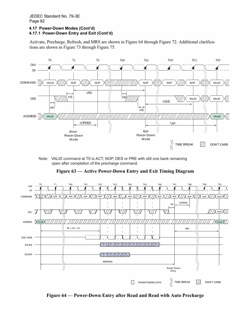
JEDEC Standard No. 79-3EPage 82
COM
AD
E
COMM
D
D
DQS,
AD
4.17 Power-Down Modes (Cont’d)4.17.1 Power-Down Entry and Exit (Cont’d)
Activate, Precharge, Refresh, and MRS are shown in Figure 64 through Figure 72. Additional clarifica-tions are shown in Figure 73 through Figure 75.
Figure 63 — Active Power-Down Entry and Exit Timing Diagram
Figure 64 — Power-Down Entry after Read and Read with Auto Precharge
CK
CK#
MAND NOP NOP NOP NOP NOP
DRESS
CKE
Enter Power-Down
Mode
ExitPower-Down
Mode
tPD
VALID
VALID
VALID
VALID
tCPDED
VALID
VALID
tIH
tIHtIS
tIS
T0 T1 T2 Ta0 Ta1 Tb0 Tb1 Tc0
NOP
tXP
tCKE
DON’T CAR()()
()()
TIME BREAK
Note: VALID command at T0 is ACT, NOP, DES or PRE with still one bank remaining open after completion of the precharge command.
T0 T1 Ta0 Ta1 Ta2 Ta3 Ta4 Ta5 Ta6 Ta7
RL = AL + CL
Ta8 Tb0
TRANSITIONING DATA
Tb1
DIN
b + 3DIN
b + 2DIN
b + 1DIN
bDIN
b + 7DIN
b + 6DIN
b + 5DIN
b + 4
NOP
VALID VALID
RD orRDA NOP NOP NOP NOP NOP NOP NOP NOP NOP NOP VALID
VALID
CK
CK#
AND
Q BL8
Q BC4
DQS#
DRESS
CKE
tCPDEDtIS
tPD
tRDPDEN
Power-Down Entry
DIN
bDIN
b + 1DIN
b + 2DIN
b + 3
DON’T CARE()()
()()
TIME BREAK
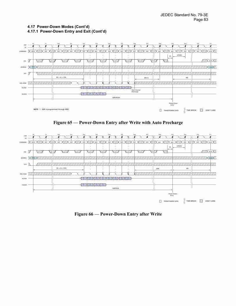
JEDEC Standard No. 79-3EPage 83
C
COMMA
DQ B
DQ B
DQS, DQ
ADDRE
A
C
ARE
C
COMMA
DQ
DQ
DQS, DQ
ADDR
A
C
RE
4.17 Power-Down Modes (Cont’d)4.17.1 Power-Down Entry and Exit (Cont’d)
Figure 65 — Power-Down Entry after Write with Auto Precharge
Figure 66 — Power-Down Entry after Write
T0 T1 Ta0 Ta1 Ta2 Ta3 Ta4 Ta5 Ta6 Ta7
WL = AL + CWL
Tb0 Tb1 Tb2 Tc0 Tc1
Bank,Col n
DIN
b + 3DIN
b + 2DIN
b + 1DIN
bDIN
b + 7DIN
b + 6DIN
b + 5DIN
b + 4
NOPWRITE NOP NOP NOP NOP NOP NOP NOP NOP NOP NOP NOP NOP
CK
K#
ND
L8
C4
S#
SS
10
KE
WR (1)
tCPDEDtIS
tPD
tWRAPDEN
Power-Down Entry
Start InternalPrecharge
DIN
n + 3DIN
n + 2DIN
n + 1DIN
n
NOTE: 1. tWR is programmed through MR0. TRANSITIONING DATA DON’T C
()()
()()
TIME BREAK
VALID
VALID
VALID
T0 T1 Ta0 Ta1 Ta2 Ta3 Ta4 Ta5 Ta6 Ta7
WL = AL + CWL
Tb0 Tb1 Tb2 Tc0 Tc1
Bank,Col n
DIN
b + 3DIN
b + 2DIN
b + 1DIN
bDIN
b + 7DIN
b + 6DIN
b + 5DIN
b + 4
NOPWRITE NOP NOP NOP NOP NOP NOP NOP NOP NOP NOP NOP NOP
CK
K#
ND
BL8
BC4
S#
ESS
10
KE
tWR
tCPDEDtIS
tPD
tWRPDEN
Power-Down Entry
DIN
n + 3DIN
n + 2DIN
n + 1DIN
n
TRANSITIONING DATA DON’T CA()()
()()
TIME BREAK
VALID
VALID
VALID
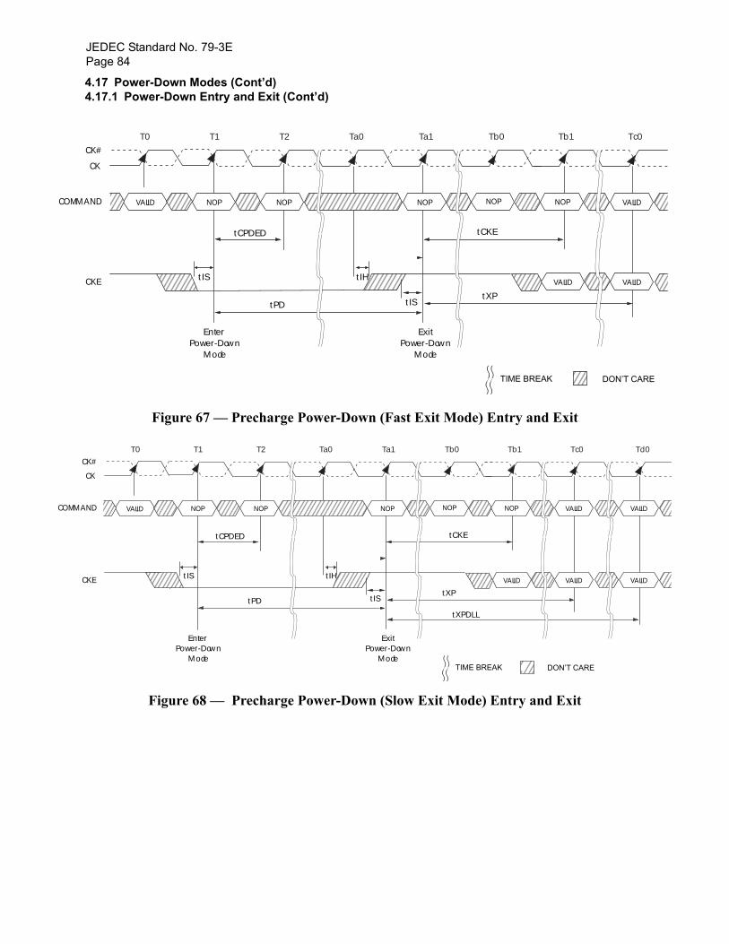
JEDEC Standard No. 79-3EPage 84
COM
COMM
4.17 Power-Down Modes (Cont’d)4.17.1 Power-Down Entry and Exit (Cont’d)
Figure 67 — Precharge Power-Down (Fast Exit Mode) Entry and Exit
Figure 68 — Precharge Power-Down (Slow Exit Mode) Entry and Exit
CK
CK#
MAND NOP NOP NOP NOP
CKE
Enter Power-Down
Mode
ExitPower-Down
Mode
tPD
VALIDVALID
tXP
tCPDED
tIS
tIHtIS
T0 T1 T2 Ta0 Ta1 Tb0 Tb1 Tc0
NOP NOP
tCKE
DON’T CARE()()
()()
TIME BREAK
VALID VALID
CK
CK#
AND NOP NOP NOP NOP
CKE
Enter Power-Down
Mode
ExitPower-Down
Mode
tPD
VALID
tXP
tXPDLL
tCPDED
tIS
tIHtIS
T0 T1 T2 Ta0 Ta1 Tb0 Tb1 Tc0
NOP NOP
tCKE
DON’T CARE()()
()()
TIME BREAK
VALID VALID
VALID
Td0
VALID
VALID
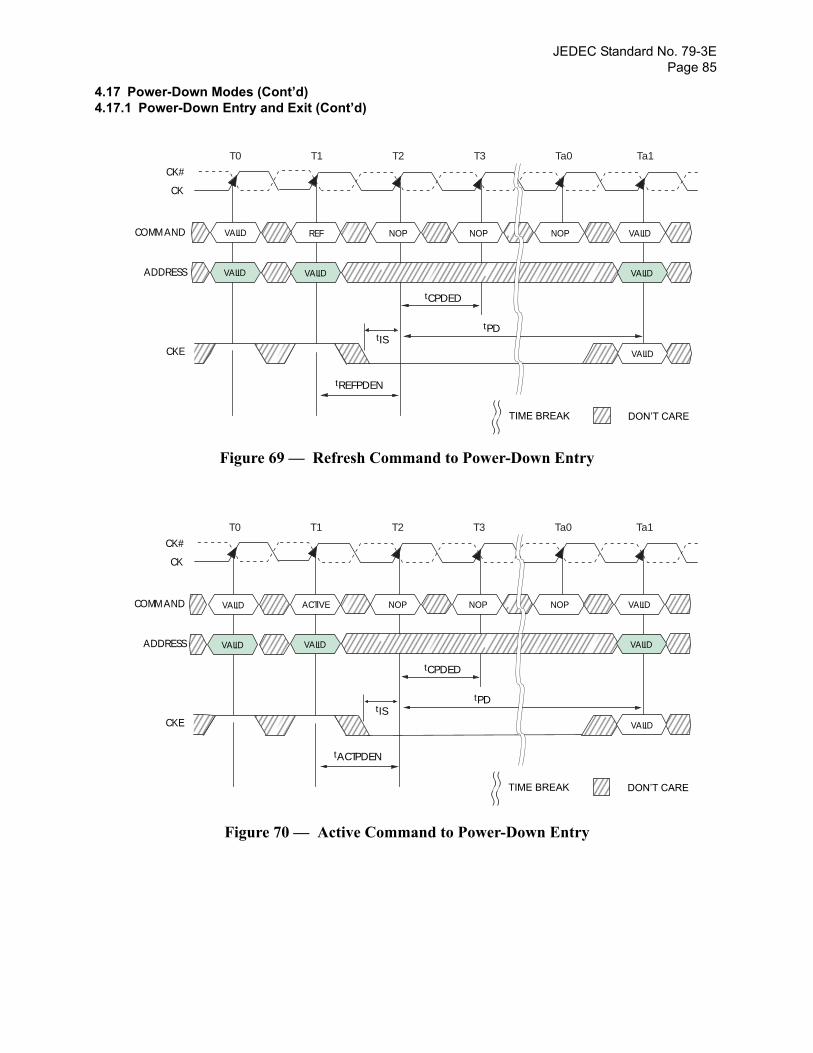
JEDEC Standard No. 79-3EPage 85
4.17 Power-Down Modes (Cont’d)4.17.1 Power-Down Entry and Exit (Cont’d)
Figure 69 — Refresh Command to Power-Down Entry
Figure 70 — Active Command to Power-Down Entry
CK
CK#
COMMAND
ADDRESS
REF NOP NOP NOP VALID
CKE
tCPDED
tREFPDEN
VALID VALID
tIS
T0 T1 T2 T3 Ta0 Ta1
tPD
DON’T CARE()()
()()
TIME BREAK
VALID
VALID
VALID
CK
CK#
COMMAND
ADDRESS
ACTIVE NOP NOP NOP VALID
CKE
tCPDED
tACTPDEN
VALID VALID
tIS
T0 T1 T2 T3 Ta0 Ta1
tPD
DON’T CARE()()
()()
TIME BREAK
VALID
VALID
VALID

JEDEC Standard No. 79-3EPage 86
4.17 Power-Down Modes (Cont’d)4.17.1 Power-Down Entry and Exit (Cont’d)
Figure 71 — Precharge / Precharge all Command to Power-Down Entry
Figure 72 — MRS Command to Power-Down Entry4.17.2 Power-Down clarifications - Case 1
When CKE is registered low for power-down entry, tPD(min) must be satisfied before CKE can be regis-tered high for power-down exit. The minimum value of parameter tPD(min) is equal to the minimum value
CK
CK#
COMMAND
ADDRESS
PRE or PREA NOP NOP NOP VALID
CKE
tCPDED
tPREPDEN
VALID VALID
tIS
T0 T1 T2 T3 Ta0 Ta1
tPD
DON’T CARE()()
()()
TIME BREAK
VALID
VALID
VALID
CK
CK#
COMMAND
ADDRESS
MRS NOPNOP NOP VALID
CKE
tCPDED
tMRSPDEN
VALID VALID
tIS
T0 T1 Ta0 Ta1 Tb0 Tb1
tPD
DON’T CARE()()
()()
TIME BREAK
VALID

JEDEC Standard No. 79-3EPage 87
4.17 Power-Down Modes (Cont’d)4.17.2 Power-Down clarifications - Case 1 (Cont’d)
of parameter tCKE(min) as shown in Table 68, Timing Parameters by Speed Bin. A detailed example of Case 1 is shown in Figure 73.
Figure 73 — Power-Down Entry/Exit Clarifications - Case 14.17.3 Power-Down clarifications - Case 2
For certain CKE intensive operations, for example, repeated ‘PD Exit - Refresh - PD Entry’ sequences, the number of clock cycles between PD Exit and PD Entry may be insufficient to keep the DLL updated. Therefore, the following conditions must be met in addition to tCKE in order to maintain proper DRAM operation when the Refresh command is issued between PD Exit and PD Entry. Power-down mode can be used in conjunction with the Refresh command if the following conditions are met: 1) tXP must be satis-fied before issuing the command. 2) tXPDLL must be satisfied (referenced to the registration of PD Exit) before the next power-down can be entered. A detailed example of Case 2 is shown in Figure 74.
Figure 74 — Power-Down Entry/Exit Clarifications - Case 2
CK
CK#
COMMAND NOP NOP NOP NOP NOP
ADDRESS
CKE
Enter Power-Down
Mode
Enter Power-Down
Mode
ExitPower-Down
Mode
tPD
NOPVALID
VALID
tCPDED tCPDED
tPD
tIH
tIHtIS
tIS
tIS
T0 T1 T2 Ta0 Ta1 Tb0 Tb1 Tb2
NOP
tCKE
DON’T CARE()()
()()
TIME BREAK
CK
CK#
COMMAND NOP NOP NOP NOP NOP
ADDRESS
CKE
Enter Power-Down
Mode
Enter Power-Down
Mode
ExitPower-Down
Mode
tPD
REFVALID
VALID
tCPDED
tIH
tIHtIS
tIS
T0 T1 T2 Ta0 Ta1 Tb0 Tb1 Tc0 Tc1 Td0
NOP NOP NOP
tXP
tXPDLL
tCKE
DON’T CARE()()
()()
TIME BREAK
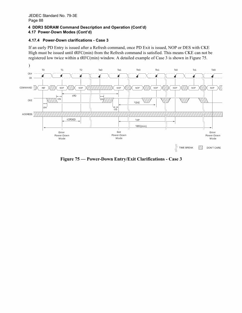
JEDEC Standard No. 79-3EPage 88
COMM
AD
n
RE
4 DDR3 SDRAM Command Description and Operation (Cont’d)4.17 Power-Down Modes (Cont’d)
4.17.4 Power-Down clarifications - Case 3
If an early PD Entry is issued after a Refresh command, once PD Exit is issued, NOP or DES with CKE High must be issued until tRFC(min) from the Refresh command is satisfied. This means CKE can not be registered low twice within a tRFC(min) window. A detailed example of Case 3 is shown in Figure 75.
)
Figure 75 — Power-Down Entry/Exit Clarifications - Case 3
CK
CK#
AND NOP NOP NOP NOP NOP
DRESS
CKE
Enter Power-Down
Mode
Enter Power-Dow
Mode
Exit Power-Down
Mode
tPD
REF
tCPDED
tIH
tIH tIS
tIS
T0 T1 T2 Ta0 Ta1 Tb0 Tb1 Tc0 Tc1 Td0
NOP NOP NOP NOP
tXP
tRFC(min)
tCKE
DON’T CA( ) ( )
( ) ( )
TIME BREAK

JEDEC Standard No. 79-3EPage 89
5 On-Die Termination (ODT)
ODT (On-Die Termination) is a feature of the DDR3 SDRAM that allows the DRAM to turn on/off termi-nation resistance for each DQ, DQS, DQS# and DM for x4 and x8 configuration (and TDQS, TDQS# for X8 configuration, when enabled via A11=1 in MR1) via the ODT control pin. For x16 configuration, ODT is applied to each DQU, DQL, DQSU, DQSU#, DQSL, DQSL#, DMU and DML signal via the ODT con-trol pin. The ODT feature is designed to improve signal integrity of the memory channel by allowing the DRAM controller to independently turn on/off termination resistance for any or all DRAM devices. More details about ODT control modes and ODT timing modes can be found further down in this document:
• The ODT control modes are described in 5.1.• The ODT synchronous mode is described in 5.2• The dynamic ODT feature is described in 5.3• The ODT asynchronous mode is described in 5.4• The transitions between ODT synchronous and asynchronous are described in 5.4.1 through 5.4.4The ODT feature is turned off and not supported in Self-Refresh mode. A simple functional representation of the DRAM ODT feature is shown in Figure 76.
Figure 76 — Functional Representation of ODTThe switch is enabled by the internal ODT control logic, which uses the external ODT pin and other con-trol information, see below. The value of RTT is determined by the settings of Mode Register bits (see Figure 10 on page 27 and Figure 11 on page 30). The ODT pin will be ignored if the Mode Registers MR1 and MR2 are programmed to disable ODT, and in self-refresh mode.
5.1 ODT Mode Register and ODT Truth TableThe ODT Mode is enabled if any of MR1 {A9, A6, A2} or MR2 {A10, A9} are non zero. In this case, the value of RTT is determined by the settings of those bits (see Figure on page 27).Application: Controller sends WR command together with ODT asserted.• One possible application: The rank that is being written to provides termination.• DRAM turns ON termination if it sees ODT asserted (unless ODT is disabled by MR).• DRAM does not use any write or read command decode information.• The Termination Truth Table is shown in Table 15.
Table 15 — Termination Truth TableODT pin DRAM Termination State
0 OFF1 ON, (OFF, if disabled by MR1 {A9, A6, A2} and MR2 {A10, A9} in general)
DQ, DQS, DM, TDQS
ODT
Switch
RTT
VDDQ / 2To other cir-cuitry like RCV, ...

JEDEC Standard No. 79-3EPage 90
5 On-Die Termination (ODT) (Cont’d)
5.2 Synchronous ODT ModeSynchronous ODT mode is selected whenever the DLL is turned on and locked. Based on the power-down definition, these modes are:
• Any bank active with CKE high• Refresh with CKE high• Idle mode with CKE high• Active power down mode (regardless of MR0 bit A12)• Precharge power down mode if DLL is enabled during precharge power down by MR0 bit A12.
The direct ODT feature is not supported during DLL-off mode. The on-die termination resistors must be disabled by continuously registering the ODT pin low and/or by programming the RTT_Nom bits MR1{A9,A6,A2} to {0,0,0} via a mode register set command during DLL-off mode.
In synchronous ODT mode, RTT will be turned on ODTLon clock cycles after ODT is sampled high by a rising clock edge and turned off ODTLoff clock cycles after ODT is registered low by a rising clock edge. The ODT latency is tied to the write latency (WL) by: ODTLon = WL - 2; ODTLoff = WL - 2 .
5.2.1 ODT Latency and Posted ODT
In Synchronous ODT Mode, the Additive Latency (AL) programmed into the Mode Register (MR1) also applies to the ODT signal. The DRAM internal ODT signal is delayed for a number of clock cycles defined by the Additive Latency (AL) relative to the external ODT signal. ODTLon = CWL + AL - 2; ODTLoff = CWL + AL - 2. For details, refer to the ODT Timing Parameters listed in Table 68 on page 169 and Table 69 on page 176.
5.2.2 Timing Parameters
In synchronous ODT mode, the following timing parameters apply (see also Figures 77):
ODTLon, ODTLoff, tAON,min,max, tAOF,min,max.
Minimum RTT turn-on time (tAONmin) is the point in time when the device leaves high impedance and ODT resistance begins to turn on. Maximum RTT turn on time (tAONmax) is the point in time when the ODT resistance is fully on. Both are measured from ODTLon.
Minimum RTT turn-off time (tAOFmin) is the point in time when the device starts to turn off the ODT resistance. Maximum RTT turn off time (tAOFmax) is the point in time when the on-die termination has reached high impedance. Both are measured from ODTLoff.
When ODT is asserted, it must remain high until ODTH4 is satisfied. If a Write command is registered by the SDRAM with ODT high, then ODT must remain high until ODTH4 (BL = 4) or ODTH8 (BL = 8) after the Write command (see Figure 78). ODTH4 and ODTH8 are measured from ODT registered high to ODT registered low or from the registration of a Write command until ODT is registered low.
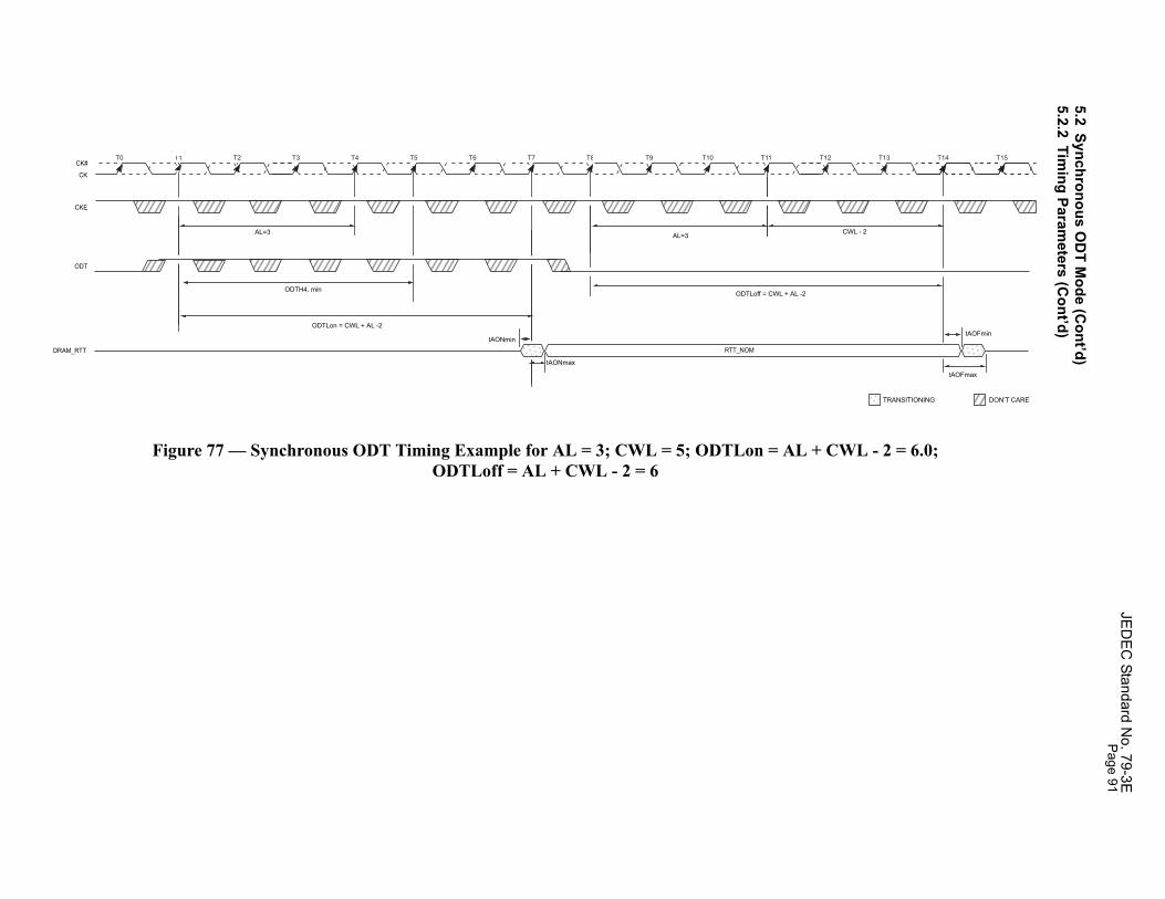
JED
EC
Standard No. 79-3EPage 91
+ CWL - 2 = 6.0;
CWL - 2
tAOFmax
tAOFmin
T12 T13 T14 T15
CK
CK#
CKE
DRAM_RTT
ODT
DON’T CARETRANSITIONING
5.2Synchronous O
DT M
ode (Cont’d)
5.2.2Tim
ing Parameters (C
ont’d)
Figure 77 — Synchronous ODT Timing Example for AL = 3; CWL = 5; ODTLon = ALODTLoff = AL + CWL - 2 = 6
T0 T1 T2 T3 T4 T5 T6 T7 T8 T9
ODTH4, min
AL=3AL=3
ODTLoff = CWL + AL -2
ODTLon = CWL + AL -2
tAONmin
tAONmax
T10 T11
RTT_NOM
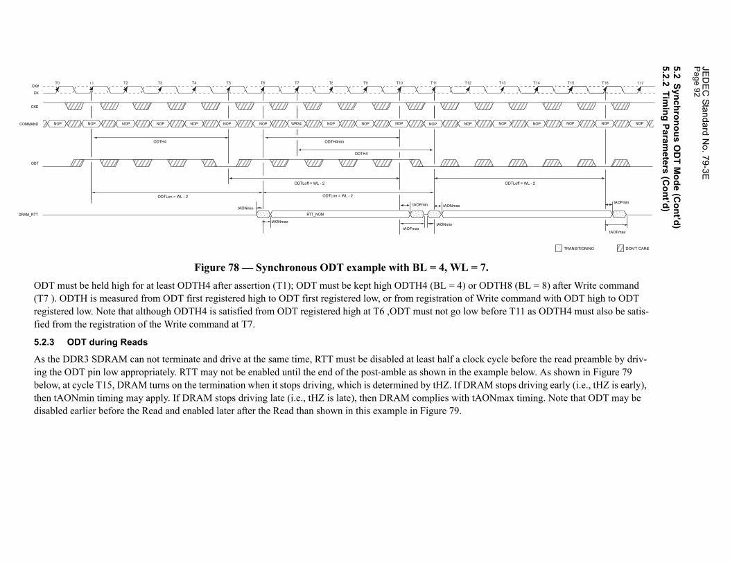
JED
EC
Standard No. 79-3E
Page 92
ODT m 8 (BL = 8) after Write command (T7 ). mmand with ODT high to ODT registe T11 as ODTH4 must also be satis-fied fr
5.2.3
As the before the read preamble by driv-ing the below. As shown in Figure 79 below, ps driving early (i.e., tHZ is early), then tA x timing. Note that ODT may be disable
T0
DTLoff = WL - 2
tAOFmax
tAOFmin
T14 T15 T17T16
CK
CK#
DRAM_RTT
ODT
CKE
NO NOP NOP NOP NOPCOMMAND
DON’T CARETRANSITIONING
5.2Synchronous O
DT M
ode (Cont’d)
5.2.2Tim
ing Parameters (C
ont’d)
Figure 78 — Synchronous ODT example with BL = 4, WL = 7. ust be held high for at least ODTH4 after assertion (T1); ODT must be kept high ODTH4 (BL = 4) or ODTH
ODTH is measured from ODT first registered high to ODT first registered low, or from registration of Write cored low. Note that although ODTH4 is satisfied from ODT registered high at T6 ,ODT must not go low beforeom the registration of the Write command at T7.
ODT during Reads
DDR3 SDRAM can not terminate and drive at the same time, RTT must be disabled at least half a clock cycle ODT pin low appropriately. RTT may not be enabled until the end of the post-amble as shown in the example at cycle T15, DRAM turns on the termination when it stops driving, which is determined by tHZ. If DRAM stoONmin timing may apply. If DRAM stops driving late (i.e., tHZ is late), then DRAM complies with tAONmad earlier before the Read and enabled later after the Read than shown in this example in Figure 79.
T1 T2 T3 T4 T5 T6 T7 T8 T9
ODTH4
ODTLon = WL - 2 ODTLon = WL - 2
ODTLoff = WL - 2 O
tAONmin
tAONmintAONmax
tAONmax
tAOFmax
tAOFmin
T10 T11 T12 T13
RTT_NOM
ODTH4min
ODTH4
NOP WRS4NOP NOP NOP NOP NOPP NOP NOP NOP NOP NOP NOP
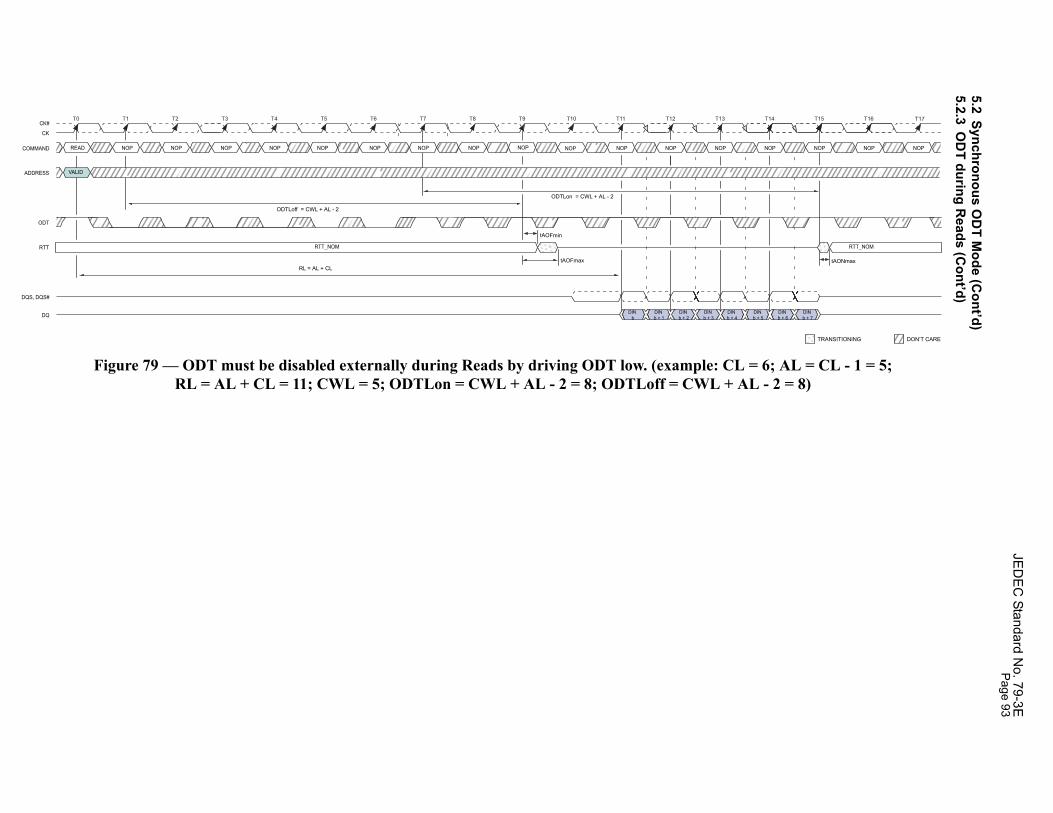
JED
EC
Standard No. 79-3EPage 93
L = 6; AL = CL - 1 = 5; AL - 2 = 8)
T0 T14 T15 T17T16
VALID
CK
CK#
COMMAND
ADDRESS
RTT
ODT
DIN b + 7
DIN b + 6
DIN b + 5
IN+ 4DQ
DQS, DQS#
RTT_NOM
tAONmax
NOP NOP NOP NOPREAD
DON’T CARETRANSITIONING
5.2Synchronous O
DT M
ode (Cont’d)
5.2.3O
DT during R
eads (Cont’d)
Figure 79 — ODT must be disabled externally during Reads by driving ODT low. (example: CRL = AL + CL = 11; CWL = 5; ODTLon = CWL + AL - 2 = 8; ODTLoff = CWL +
T1 T2 T3 T4 T5 T6 T7 T8 T9
RL = AL + CL
ODTLoff = CWL + AL - 2
ODTLon = CWL + AL - 2
T10 T11 T12 T13
NOP NOP NOP NOP NOP NOP NOP
RTT_NOM
DIN b + 3
DIN b + 2
DIN b + 1
DIN b
D b
RTT_NOM
tAOFmin
tAOFmax
NOP NOP NOP NOP NOPNOP
RTT_NOM

JEDEC Standard No. 79-3EPage 94
N
O
OD
O
O )
5 On-Die Termination (ODT) (Cont’d)
5.3 Dynamic ODTIn certain application cases and to further enhance signal integrity on the data bus, it is desirable that the termination strength of the DDR3 SDRAM can be changed without issuing an MRS command. This requirement is supported by the “Dynamic ODT” feature as described as follows:
5.3.1 Functional Description:
The Dynamic ODT Mode is enabled if bit (A9) or (A10) of MR2 is set to ’1’. The function is described as follows:
• Two RTT values are available: RTT_Nom and RTT_WR.• The value for RTT_Nom is preselected via bits A[9,6,2] in MR1.• The value for RTT_WR is preselected via bits A[10,9] in MR2.
• During operation without write commands, the termination is controlled as follows:• Nominal termination strength RTT_Nom is selected.• Termination on/off timing is controlled via ODT pin and latencies ODTLon and ODTLoff.
• When a write command (WR, WRA, WRS4, WRS8, WRAS4, WRAS8) is registered, and if Dynamic ODT is enabled, the termination is controlled as follows:• A latency ODTLcnw after the write command, termination strength RTT_WR is selected.• A latency ODTLcwn8 (for BL8, fixed by MRS or selected OTF) or ODTLcwn4 (for BC4, fixed by
MRS or selected OTF) after the write command, termination strength RTT_Nom is selected.• Termination on/off timing is controlled via ODT pin and ODTLon, ODTLoff.
Table 16 shows latencies and timing parameters which are relevant for the on-die termination control in Dynamic ODT mode.
The dynamic ODT feature is not supported at DLL-off mode. User must use MRS command to set Rtt_WR, MR2{A10, A9}={0,0}, to disable Dynamic ODT externally.
When ODT is asserted, it must remain high until ODTH4 is satisfied. If a Write command is registered by the SDRAM with ODT high, then ODT must remain high until ODTH4 (BL = 4) or ODTH8 (BL = 8) after the Write command (see Figure 78). ODTH4 and ODTH8 are measured from ODT registered high to ODT registered low or from the registration of a Write command until ODT is registered low.:
Table 16 — Latencies and timing parameters relevant for Dynamic ODT
ame and Description Abbr. Defined from Defined toDefinition for all DDR3 speed
bins Unit
ODT turn-on Latency ODTLon registering external ODT signal high
turning termination on ODTLon = WL – 2 tCK
DT turn-off Latency ODTLoff registering external ODT signal low
turning termination off ODTLoff = WL – 2 tCK
T Latency for changing from RTT_Nom to
RTT_WR
ODTLcnw registering external write command
change RTT strength from RTT_Nom to RTT_WR
ODTLcnw = WL – 2 tCK
DT Latency for change from RTT_WR to
RTT_Nom (BL = 4)
ODTLcwn4 registering external write command
change RTT strength from RTT_WR to RTT_Nom
ODTLcwn4 =4 + ODTLoff
tCK
DT Latency for change from RTT_WR to
RTT_Nom (BL = 8)
ODTLcwn8 registering external write command
change RTT strength from RTT_WR to RTT_Nom
ODTLcwn8 =6 + ODTLoff
tCK(avg
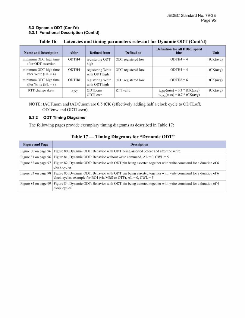
JEDEC Standard No. 79-3EPage 95
m )
m )
m )
)
F
FiguFiguFigu
Figu
Figu
N
5.3 Dynamic ODT (Cont’d)5.3.1 Functional Description (Cont’d)
NOTE: tAOF,nom and tADC,nom are 0.5 tCK (effectively adding half a clock cycle to ODTLoff, ODTcnw and ODTLcwn)
5.3.2 ODT Timing Diagrams
The following pages provide exemplary timing diagrams as described in Table 17:
inimum ODT high time after ODT assertion
ODTH4 registering ODT high
ODT registered low ODTH4 = 4 tCK(avg
inimum ODT high time after Write (BL = 4)
ODTH4 registering Write with ODT high
ODT registered low ODTH4 = 4 tCK(avg
inimum ODT high time after Write (BL = 8)
ODTH8 registering Write with ODT high
ODT registered low ODTH8 = 6 tCK(avg
RTT change skew tADC ODTLcnwODTLcwn
RTT valid tADC(min) = 0.3 * tCK(avg)tADC(max) = 0.7 * tCK(avg)
tCK(avg
Table 17 — Timing Diagrams for “Dynamic ODT”igure and Page Description
re 80 on page 96 Figure 80, Dynamic ODT: Behavior with ODT being asserted before and after the write.re 81 on page 96 Figure 81, Dynamic ODT: Behavior without write command, AL = 0, CWL = 5.re 82 on page 97 Figure 82, Dynamic ODT: Behavior with ODT pin being asserted together with write command for a duration of 6
clock cycles.re 83 on page 98 Figure 83, Dynamic ODT: Behavior with ODT pin being asserted together with write command for a duration of 6
clock cycles, example for BC4 (via MRS or OTF), AL = 0, CWL = 5.re 84 on page 99 Figure 84, Dynamic ODT: Behavior with ODT pin being asserted together with write command for a duration of 4
clock cycles.
Table 16 — Latencies and timing parameters relevant for Dynamic ODT (Cont’d)
ame and Description Abbr. Defined from Defined toDefinition for all DDR3 speed
bins Unit
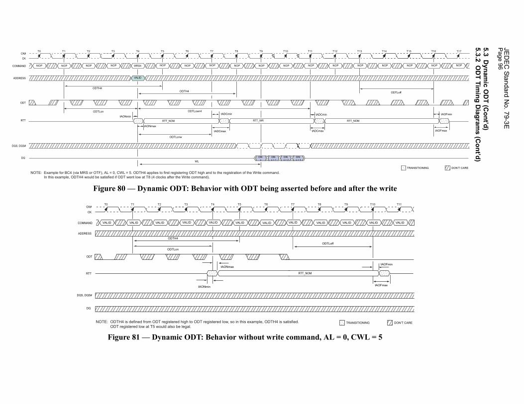
JED
EC
Standard No. 79-3E
Page 96
the write
L = 5
T0 T1 T2 T3 T4 T5 T6 T7 T8 T9
ODTLoff
tAOFmax
tAOFmin
T10 T11 T12 T13 T14 T15 T17T16
CK
CK#
COMMAND
ADDRESS
RTT
ODT
DQ
DQS, DQS#
NOP NOP NOP NOP NOP
DON’T CARETRANSITIONING
NOTE:
tAOFmin
tAOFmax
T10 T11
DON’T CAREING
VALID VALID
5.3D
ynamic O
DT (C
ont’d)5.3.2
OD
T Timing D
iagrams (C
ont’d)
Figure 80 — Dynamic ODT: Behavior with ODT being asserted before and after
Figure 81 — Dynamic ODT: Behavior without write command, AL = 0, CW
ODTH4ODTH4
ODTLon ODTLcwn4
ODTLcnw
WL
tAONmin
tAONmax
tADCmax tADCmax
tADCmin tADCmin
RTT_NOM RTT_NOM
VALID
RTT_WR
WRS4NOP NOP NOP NOP NOP NOP NOP NOP NOP NOP NOP NOP
DIN n + 3
DIN n + 2
DIN n + 1
DIN n
Example for BC4 (via MRS or OTF), AL = 0, CWL = 5. ODTH4 applies to first registering ODT high and to the registration of the Write command. In this example, ODTH4 would be satisfied if ODT went low at T8 (4 clocks after the Write command).
T0 T1 T2 T3 T4 T5 T6 T7 T8 T9
ODTLoff
ODTH4
ODTLon
tAONmin
tAONmax
CK
CK#
ADDRESS
RTT
ODT
DQ
DQS, DQS#
RTT_NOM
TRANSITION
COMMAND VALID VALID VALID VALID VALID VALID VALID VALID VALID VALID
NOTE: ODTH4 is defined from ODT registered high to ODT registered low, so in this example, ODTH4 is satisfied. ODT registered low at T5 would also be legal.
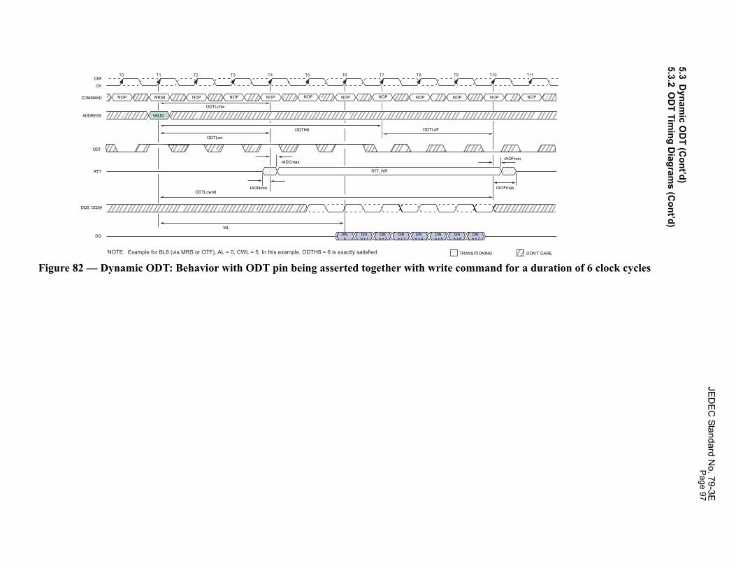
JED
EC
Standard No. 79-3EPage 97
Figu r a duration of 6 clock cycles
Fmin
x
T11
DON’T CARE
NOP
5.3D
ynamic O
DT (C
ont’d)5.3.2
OD
T Timing D
iagrams (C
ont’d)
re 82 — Dynamic ODT: Behavior with ODT pin being asserted together with write command fo
T0 T1 T2 T3 T4 T5 T6 T7 T8 T9
ODTLoff ODTH8
ODTLcwn8
ODTLon
ODTLcnw
WL
tAO
tAONmin tAOFma
tADCmax
T10
CK
CK#
ADDRESS
RTT
ODT
DQ
DQS, DQS#
RTT_WR
DIN b + 3
DIN b + 2
DIN b + 1
DIN b
DIN b + 7
DIN b + 6
DIN b + 5
DIN b + 4
VALID
TRANSITIONING
COMMAND WRS8NOP NOPNOP NOP NOP NOP NOP NOP NOP NOP
NOTE: Example for BL8 (via MRS or OTF), AL = 0, CWL = 5. In this example, ODTH8 = 6 is exactly satisfied.
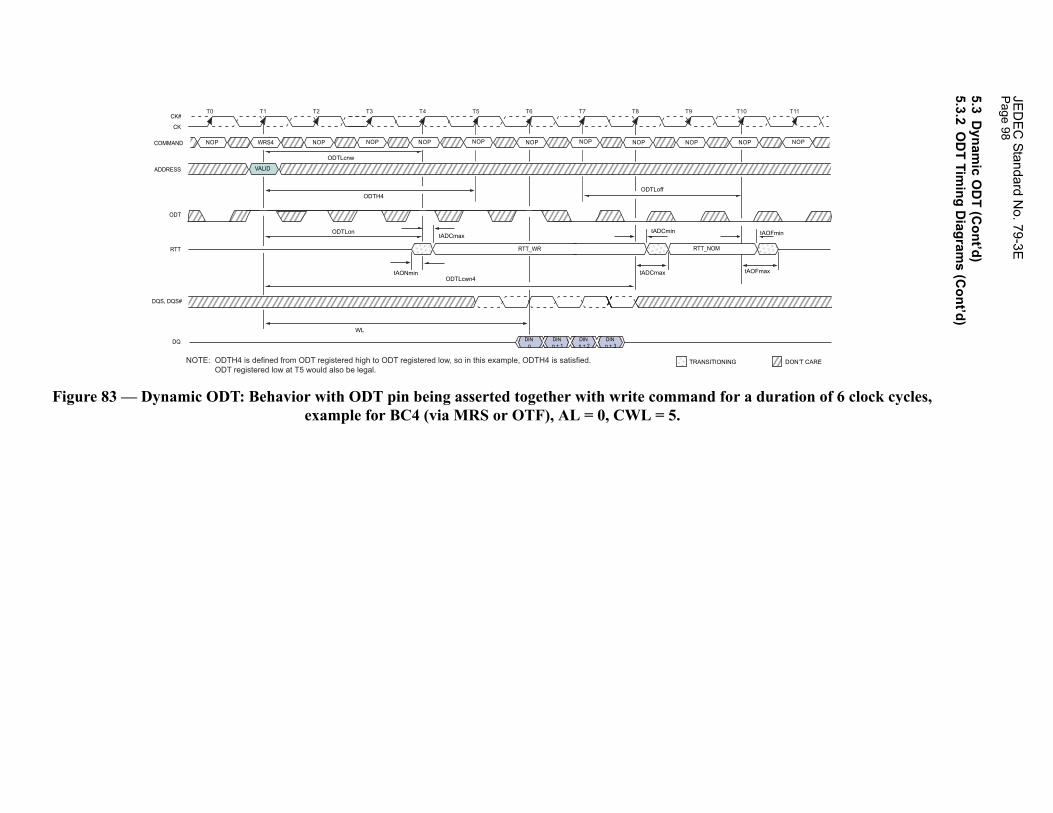
JED
EC
Standard No. 79-3E
Page 98
Figur r a duration of 6 clock cycles,
tAOFmin
tAOFmax
T10 T11
NOP NOP
DON’T CAREG
5.3D
ynamic O
DT (C
ont’d)5.3.2
OD
T Timing D
iagrams (C
ont’d)
e 83 — Dynamic ODT: Behavior with ODT pin being asserted together with write command foexample for BC4 (via MRS or OTF), AL = 0, CWL = 5.
T0 T1 T2 T3 T4 T5 T6 T7 T8 T9
ODTLoff
ODTLcwn4
ODTLon
ODTH4
ODTLcnw
WL
tADCmin
tAONmin tADCmax
tADCmax
CK
CK#
ADDRESS
RTT
ODT
DQ
DQS, DQS#
VALID
DIN n + 3
DIN n + 2
DIN n + 1
DIN n
RTT_WR RTT_NOM
COMMAND WRS4NOP NOPNOP NOP NOP NOP NOP NOP NOP
TRANSITIONINNOTE: ODTH4 is defined from ODT registered high to ODT registered low, so in this example, ODTH4 is satisfied. ODT registered low at T5 would also be legal.

JED
EC
Standard No. 79-3EPage 99
Figu r a duration of 4 clock cycles
T10 T11
NOP NOP
DON’T CAREG
5.3D
ynamic O
DT (C
ont’d)5.3.2
OD
T Timing D
iagrams (C
ont’d)
re 84 — Dynamic ODT: Behavior with ODT pin being asserted together with write command fo
T0 T1 T2 T3 T4 T5 T6 T7 T8 T9
ODTLoff
ODTLcwn4
ODTLon
ODTH4
ODTLcnw
WL
tAOFmin
tAONmin tAOFmax
tADCmax
CK
CK#
ADDRESS
RTT
ODT
DQ
DQS, DQS#
VALID
DIN n + 3
DIN n + 2
DIN n + 1
DIN n
RTT_WR
COMMAND WRS4NOP NOPNOP NOP NOP NOP NOP NOP NOP
TRANSITIONINNOTE: Example for BC4 (via MRS or OTF), AL = 0, CWL = 5. In this example, ODTH4 = 4 is exactly satisfied.
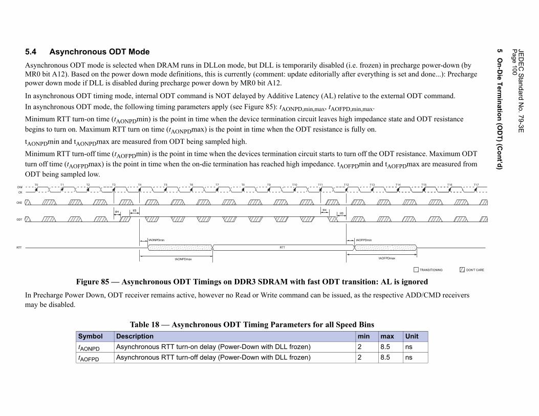
JED
EC
Standard No. 79-3E
Page 100
5.4Async n) in precharge power-down (by MR0 b thing is set and done...): Precharge power
In asy e external ODT command.In asy Minim nce state and ODT resistance begins . tAONP
Minim e ODT resistance. Maximum ODT turn of nd tAOFPDmax are measured from ODT b
: AL is ignoredIn Pre espective ADD/CMD receivers may b
max Unit8.5 ns8.5 ns
T0
tAOFPDmax
T14 T15 T17T16
CK
CK#
RTT
ODT
CKE
DON’T CARETRANSITIONING
5 O
n-Die Term
ination (OD
T) (Cont’d)
Asynchronous ODT Modehronous ODT mode is selected when DRAM runs in DLLon mode, but DLL is temporarily disabled (i.e. frozeit A12). Based on the power down mode definitions, this is currently (comment: update editorially after every
down mode if DLL is disabled during precharge power down by MR0 bit A12.
nchronous ODT timing mode, internal ODT command is NOT delayed by Additive Latency (AL) relative to thnchronous ODT mode, the following timing parameters apply (see Figure 85): tAONPD,min,max, tAOFPD,min,max.um RTT turn-on time (tAONPDmin) is the point in time when the device termination circuit leaves high impeda to turn on. Maximum RTT turn on time (tAONPDmax) is the point in time when the ODT resistance is fully on
Dmin and tAONPDmax are measured from ODT being sampled high.um RTT turn-off time (tAOFPDmin) is the point in time when the devices termination circuit starts to turn off thf time (tAOFPDmax) is the point in time when the on-die termination has reached high impedance. tAOFPDmin aeing sampled low.
Figure 85 — Asynchronous ODT Timings on DDR3 SDRAM with fast ODT transitioncharge Power Down, ODT receiver remains active, however no Read or Write command can be issued, as the re disabled.
Table 18 — Asynchronous ODT Timing Parameters for all Speed BinsSymbol Description mintAONPD Asynchronous RTT turn-on delay (Power-Down with DLL frozen) 2tAOFPD Asynchronous RTT turn-off delay (Power-Down with DLL frozen) 2
T1 T2 T3 T4 T5 T6 T7 T8 T9
tAONPDmin
tIStIStIH tIH
tAONPDmax
tAOFPDmin
T10 T11 T12 T13
RTT
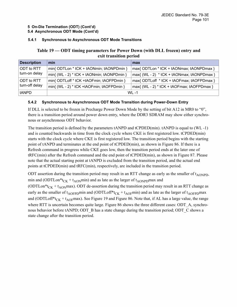
JEDEC Standard No. 79-3EPage 101
DeODturn
}}
ODturn
}
tAN
5 On-Die Termination (ODT) (Cont’d)5.4 Asynchronous ODT Mode (Cont’d)
5.4.1 Synchronous to Asynchronous ODT Mode Transitions
5.4.2 Synchronous to Asynchronous ODT Mode Transition during Power-Down Entry
If DLL is selected to be frozen in Precharge Power Down Mode by the setting of bit A12 in MR0 to “0”, there is a transition period around power down entry, where the DDR3 SDRAM may show either synchro-nous or asynchronous ODT behavior.
The transition period is defined by the parameters tANPD and tCPDED(min). tANPD is equal to (WL -1) and is counted backwards in time from the clock cycle where CKE is first registered low. tCPDED(min) starts with the clock cycle where CKE is first registered low. The transition period begins with the starting point of tANPD and terminates at the end point of tCPDED(min), as shown in Figure 86. If there is a Refresh command in progress while CKE goes low, then the transition period ends at the later one of tRFC(min) after the Refresh command and the end point of tCPDED(min), as shown in Figure 87. Please note that the actual starting point at tANPD is excluded from the transition period, and the actual end points at tCPDED(min) and tRFC(min), respectively, are included in the transition period.
ODT assertion during the transition period may result in an RTT change as early as the smaller of tAONPD-min and (ODTLon*tCK + tAONmin) and as late as the larger of tAONPDmax and (ODTLon*tCK + tAONmax). ODT de-assertion during the transition period may result in an RTT change as early as the smaller of tAOFPDmin and (ODTLoff*tCK + tAOFmin) and as late as the larger of tAOFPDmax and (ODTLoff*tCK + tAOFmax). See Figure 19 and Figure 86. Note that, if AL has a large value, the range where RTT is uncertain becomes quite large. Figure 86 shows the three different cases: ODT_A, synchro-nous behavior before tANPD; ODT_B has a state change during the transition period; ODT_C shows a state change after the transition period.
Table 19 — ODT timing parameters for Power Down (with DLL frozen) entry and exit transition period
scription min maxT to RTT -on delay
min{ ODTLon * tCK + tAONmin; tAONPDmin } max{ ODTLon * tCK + tAONmax; tAONPDmax min{ (WL - 2) * tCK + tAONmin; tAONPDmin } max{ (WL - 2) * tCK + tAONmax; tAONPDmax
T to RTT -off delay
min{ ODTLoff * tCK +tAOFmin; tAOFPDmin } max{ ODTLoff * tCK + tAOFmax; tAOFPDmax min{ (WL - 2) * tCK +tAOFmin; tAOFPDmin } max{ (WL - 2) * tCK + tAOFmax; tAOFPDmax }
PD WL -1
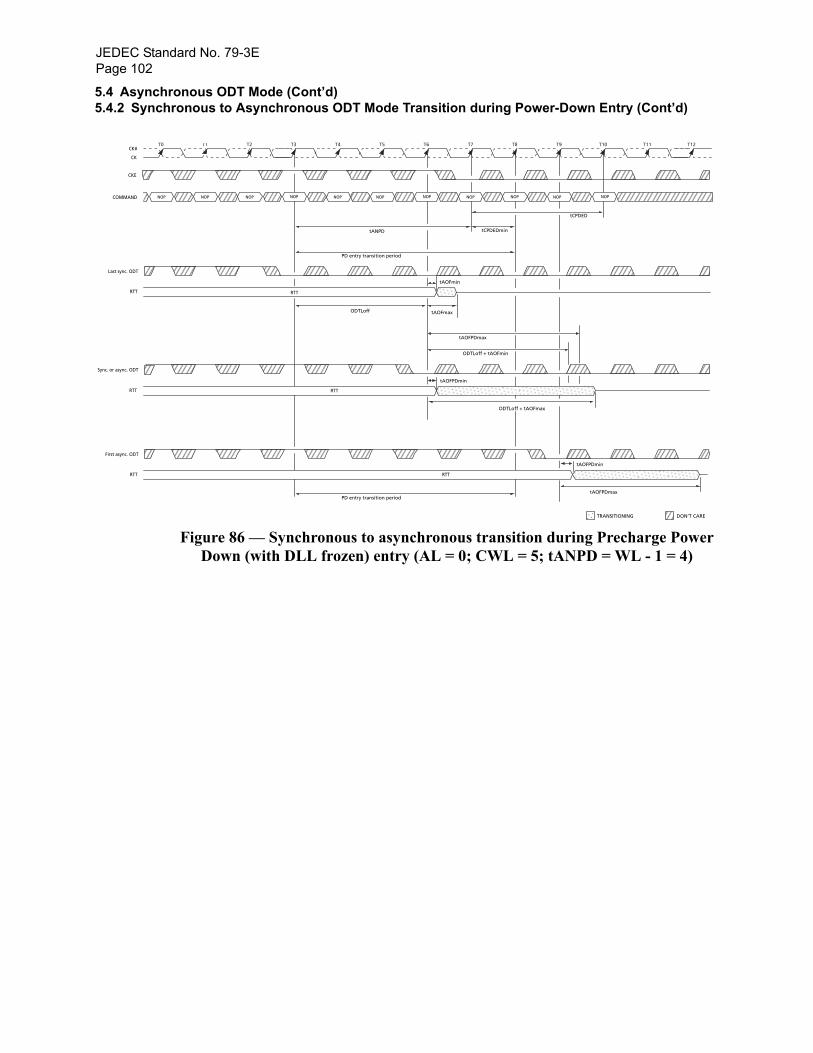
JEDEC Standard No. 79-3EPage 102
5.4 Asynchronous ODT Mode (Cont’d)5.4.2 Synchronous to Asynchronous ODT Mode Transition during Power-Down Entry (Cont’d)
Figure 86 — Synchronous to asynchronous transition during Precharge Power Down (with DLL frozen) entry (AL = 0; CWL = 5; tANPD = WL - 1 = 4)
T0 T1 T2 T3 T4 T5 T6 T7 T8 T9
tAOFPDmax
tAOFmax
tAOFPDmax
tAOFPDmin
tAOFmin
ODTLoff
tANPD
PD entry transition period
tAOFPDmin
ODTLoff + tAOFmin
T10 T11 T12
CK
CK#
RTT
RTT
RTT
Last sync. ODT
CKE
Sync. or async. ODT
First async. ODT
NOP NOP NOPNOPCOMMAND
PD entry transition period
NOP NOP NOP
RTT
RTT
RTT
DON’T CARETRANSITIONING
NOP NOP
tCPDEDmin
tCPDED
NOPNOP
ODTLoff + tAOFmax
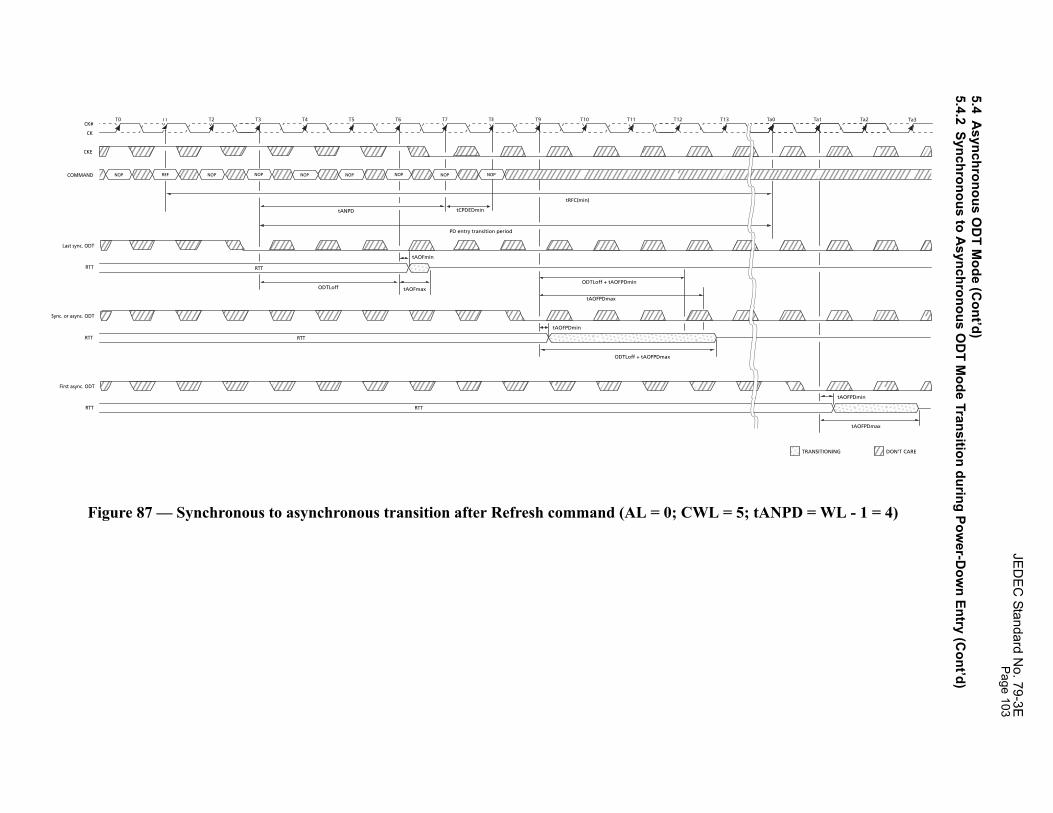
JED
EC
Standard No. 79-3EPage 103
5; tANPD = WL - 1 = 4)
tAOFPDmax
tAOFPDmin
Ta0 Ta1 Ta3Ta2
Last sync.
C
Sync. or async.
First async.
COMMA
DON’T CARETRANSITIONING
5.4A
synchronous OD
T Mode (C
ont’d)5.4.2
Synchronous to Asynchronous O
DT M
ode Transition during Power-D
own Entry (C
ont’d)
Figure 87 — Synchronous to asynchronous transition after Refresh command (AL = 0; CWL =
T0 T1 T2 T3 T4 T5 T6 T7 T8 T9
tAOFmax
ODTLoff + tAOFPDmax
ODTLoff + tAOFPDmin
tAOFmin
ODTLoff
tANPD
tRFC(min)
PD entry transition period
tAOFPDmin
tAOFPDmax
T10 T11 T12 T13
CK
CK#
RTT
RTT
RTT
ODT
KE
ODT
ODT
NOP NOP NOPNOPND NOPREF NOP NOP
RTT
RTT
RTT
tCPDEDmin
NOP
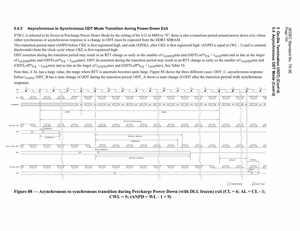
JED
EC
Standard No. 79-3E
Page 104
5.4.3 Asynchronous to Synchronous ODT Mode Transition during Power-Down Exit
If DLL eriod around power down exit, where either sThis tra D is equal to (WL - 1) and is counted (backwODT a + tAONmin) and as late as the larger of tAON rly as the smaller of tAOFPDmin and (ODTL
Note th es: ODT_C, asynchronous response before nsition period with synchronous respon
Figur n) exit (CL = 6; AL = CL - 1;
tAOFmaxODTLoff
tAOFmin
Tc1 Td0 Td1Tc2
CK
CK#
RTT
RTT
RTT
DON’T CARETRANSITIONING
Last async. ODT
CKE
Sync. or async. ODT
First sync. ODT
COMMAND NOP NOP NOP NOP
5O
n-Die Term
ination (OD
T) (Cont’d)
5.4A
synchronous OD
T Mode (C
ont’d)
is selected to be frozen in Precharge Power Down Mode by the setting of bit A12 in MR0 to “0”, there is also a transition pynchronous or asynchronous response to a change in ODT must be expected from the DDR3 SDRAM.nsition period starts tANPD before CKE is first registered high, and ends tXPDLL after CKE is first registered high. tANPards) from the clock cycle where CKE is first registered high. ssertion during the transition period may result in an RTT change as early as the smaller of tAONPDmin and (ODTLon*tCK
PDmax and (ODTLon*tCK + tAONmax). ODT de-assertion during the transition period may result in an RTT change as eaoff*tCK + tAOFmin) and as late as the larger of tAOFPDmax and (ODTLoff*tCK + tAOFmax). See Table 19.
at, if AL has a large value, the range where RTT is uncertain becomes quite large. Figure 88 shows the three different castANPD; ODT_B has a state change of ODT during the transition period; ODT_A shows a state change of ODT after the trase.
e 88 — Asynchronous to synchronous transition during Precharge Power Down (with DLL frozeCWL = 5; tANPD = WL - 1 = 9)
T0 T1 T2 Ta0 Ta1 Ta2 Ta3 Ta4 Ta5 Ta6
tAOFPDmax
ODTLoff + tAOFmax
ODTLoff + tAOFmin
tAOFPDmin
tANPD tXPDLL
PD exit transition period
tAOFPDmin
tAOFPDmax
Tb0 Tb1 Tb2 Tc0
NOP NOPNOP NOP NOP NOP NOP NOP
RTT
RTT
RTT
NOPNOP

JED
EC
Standard No. 79-3EPage 105
5.4.4
If the t xit may overlap (see Figure 89). In this ca nchronous from the start of the PD entry t od).
If the e response of the DDR3 SDRAMs RTT to ion period to the end of the PD entry t progress when Idle state was entere
lapping
T12 T13 T14
NOP NOP NOPCOM
DON’T CARETRANSITIONING
5O
n-Die Term
ination (OD
T) (Cont’d)
5.4A
synchronous OD
T Mode (C
ont’d)
Asynchronous to Synchronous ODT Mode during short CKE high and short CKE low periodsotal time in Precharge Power Down state or Idle state is very short, the transition periods for PD entry and PD ese, the response of the DDR3 SDRAMs RTT to a change in ODT state at the input may be synchronous OR asyransition period to the end of the PD exit transition period (even if the entry period ends later than the exit peri
total time in Idle state is very short, the transition periods for PD exit and PD entry may overlap. In this case th a change in ODT state at the input may be synchronous OR asynchronous from the start of the PD exit transit
ransition period. Note that in the bottom part of Figure 89 it is assumed that there was no Refresh command ind.
Figure 89 — Transition period for short CKE cycles, entry and exit period over(AL = 0, WL = 5, tANPD = WL - 1 = 4)
T0 T1 T2 T3 T4 T5 T6 T7 T8 T9 T10 T11
CK
CK#
CKE
NOP NOP NOP NOP NOP NOPMAND NOPREF NOP NOP
CKE
NOP
tANPD
tANPD
tANPD
tXPDLL
short CKE high transition period
PD exit transition period
tXPDLL
short CKE low transition period
PD entry transition period
tRFC(min)
NOP

JEDEC Standard No. 79-3EPage 106
This page left blank.
JEDEC Standard No. 79-3EPage 107
4 DDR3 SDRAM Command Description and Operation (Cont’d)
5.5 ZQ Calibration Commands5.5.1 ZQ Calibration Description
ZQ Calibration command is used to calibrate DRAM Ron & ODT values. DDR3 SDRAM needs longer time to calibrate output driver and on-die termination circuits at initialization and relatively smaller time to perform periodic calibrations.
ZQCL command is used to perform the initial calibration during power-up initialization sequence. This command may be issued at any time by the controller depending on the system environment. ZQCL com-mand triggers the calibration engine inside the DRAM and, once calibration is achieved, the calibrated val-ues are transferred from the calibration engine to DRAM IO, which gets reflected as updated output driver and on-die termination values.
The first ZQCL command issued after reset is allowed a timing period of tZQinit to perform the full cali-bration and the transfer of values. All other ZQCL commands except the first ZQCL command issued after RESET are allowed a timing period of tZQoper.
ZQCS command is used to perform periodic calibrations to account for voltage and temperature variations. A shorter timing window is provided to perform the calibration and transfer of values as defined by timing parameter tZQCS. One ZQCS command can effectively correct a minimum of 0.5 % (ZQ Correction) of RON and RTT impedance error within 64 nCK for all speed bins assuming the maximum sensitivities specified in the ‘Output Driver Voltage and Temperature Sensitivity’ and ‘ODT Voltage and Temperature Sensitivity’ tables. The appropriate interval between ZQCS commands can be determined from these tables and other application-specific parameters. One method for calculating the interval between ZQCS commands, given the temperature (Tdriftrate) and voltage (Vdriftrate) drift rates that the SDRAM is sub-ject to in the application, is illustrated. The interval could be defined by the following formula:
where TSens = max(dRTTdT, dRONdTM) and VSens = max(dRTTdV, dRONdVM) define the SDRAM temperature and voltage sensitivities.
For example, if TSens = 1.5% / oC, VSens = 0.15% / mV, Tdriftrate = 1 oC / sec and Vdriftrate = 15 mV / sec, then the interval between ZQCS commands is calculated as:
No other activities should be performed on the DRAM channel by the controller for the duration of tZQinit, tZQoper, or tZQCS. The quiet time on the DRAM channel allows accurate calibration of output driver and on-die termination values. Once DRAM calibration is achieved, the DRAM should disable ZQ current consumption path to reduce power.
All banks must be precharged and tRP met before ZQCL or ZQCS commands are issued by the controller. See “[BA=Bank Address, RA=Row Address, CA=Column Address, BC#=Burst Chop, X=Don’t Care, V=Valid]” on page 33 for a description of the ZQCL and ZQCS commands.
ZQ calibration commands can also be issued in parallel to DLL lock time when coming out of self refresh. Upon Self-Refresh exit, DDR3 SDRAM will not perform an IO calibration without an explicit ZQ calibra-tion command. The earliest possible time for ZQ Calibration command (short or long) after self refresh exit is tXS.
ZQCorrectionTSens Tdriftrate×( ) VSens Vdriftrate×( )+
-----------------------------------------------------------------------------------------------------------------
0.51.5 1×( ) 0.15 15×( )+
------------------------------------------------------- 0.133= 128ms≈
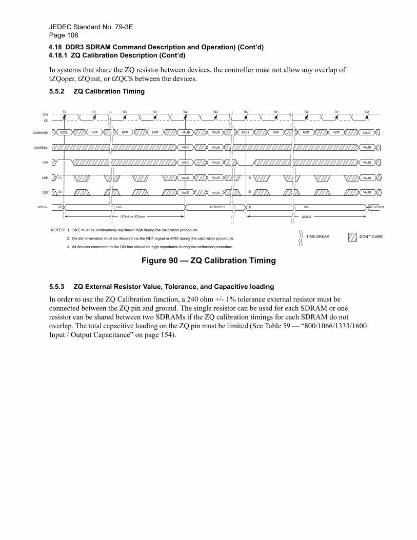
JEDEC Standard No. 79-3EPage 108
VITIES
C
COMMA
ADDRE
C
A
DQ B
O
ARE
4.18 DDR3 SDRAM Command Description and Operation) (Cont’d)4.18.1 ZQ Calibration Description (Cont’d)
In systems that share the ZQ resistor between devices, the controller must not allow any overlap of tZQoper, tZQinit, or tZQCS between the devices.
5.5.2 ZQ Calibration Timing
Figure 90 — ZQ Calibration Timing
5.5.3 ZQ External Resistor Value, Tolerance, and Capacitive loading
In order to use the ZQ Calibration function, a 240 ohm +/- 1% tolerance external resistor must be connected between the ZQ pin and ground. The single resistor can be used for each SDRAM or one resistor can be shared between two SDRAMs if the ZQ calibration timings for each SDRAM do not overlap. The total capacitive loading on the ZQ pin must be limited (See Table 59 — “800/1066/1333/1600 Input / Output Capacitance” on page 154).
T0 T1 Ta0 Ta1 Ta2 Ta3 Tb0 Tb1 Tc0 Tc1 Tc2
NOTES: 1. CKE must be continuously registered high during the calibration procedure.
2. On-die termination must be disabled via the ODT signal or MRS during the calibration procedure.
3. All devices connected to the DQ bus should be high impedance during the calibration procedure.
VALID
VALID
VALID
VALID
VALID
VALID
VALID
VALID
NOPZQCL
HI-Z HI-ZACTIVITIES ACTI
NOP NOP VALID VALID
VALID
VALID
VALID
VALID
ZQCS NOP NOP NOP VALID
CK
K#
ND
SS
KE
10
us
tZQCS
DT
tZQinit or tZQoper
(1)
(2)
(3)
(1)
(2)
(3)
DON’T C()()
()()
TIME BREAK
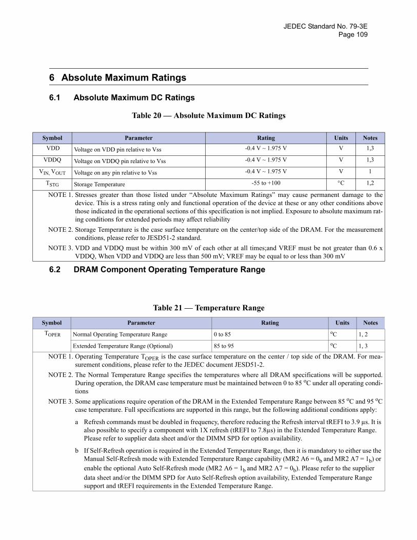
JEDEC Standard No. 79-3EPage 109
S s
V
heveat-
nt
x
S s
a-
ed.di-
oC:
is .
he or
6 Absolute Maximum Ratings
6.1 Absolute Maximum DC Ratings
Table 20 — Absolute Maximum DC Ratings
6.2 DRAM Component Operating Temperature Range
ymbol Parameter Rating Units Note
VDD Voltage on VDD pin relative to Vss -0.4 V ~ 1.975 V V 1,3
VDDQ Voltage on VDDQ pin relative to Vss -0.4 V ~ 1.975 V V 1,3
IN, VOUT Voltage on any pin relative to Vss -0.4 V ~ 1.975 V V 1
TSTG Storage Temperature -55 to +100 °C 1,2
NOTE 1. Stresses greater than those listed under “Absolute Maximum Ratings” may cause permanent damage to tdevice. This is a stress rating only and functional operation of the device at these or any other conditions abothose indicated in the operational sections of this specification is not implied. Exposure to absolute maximum ring conditions for extended periods may affect reliability
NOTE 2. Storage Temperature is the case surface temperature on the center/top side of the DRAM. For the measuremeconditions, please refer to JESD51-2 standard.
NOTE 3. VDD and VDDQ must be within 300 mV of each other at all times;and VREF must be not greater than 0.6VDDQ, When VDD and VDDQ are less than 500 mV; VREF may be equal to or less than 300 mV
Table 21 — Temperature Range
ymbol Parameter Rating Units Note
TOPER Normal Operating Temperature Range 0 to 85 oC 1, 2
Extended Temperature Range (Optional) 85 to 95 oC 1, 3
NOTE 1. Operating Temperature TOPER is the case surface temperature on the center / top side of the DRAM. For mesurement conditions, please refer to the JEDEC document JESD51-2.
NOTE 2. The Normal Temperature Range specifies the temperatures where all DRAM specifications will be supportDuring operation, the DRAM case temperature must be maintained between 0 to 85 oC under all operating contions
NOTE 3. Some applications require operation of the DRAM in the Extended Temperature Range between 85 oC and 95 case temperature. Full specifications are supported in this range, but the following additional conditions apply
a Refresh commands must be doubled in frequency, therefore reducing the Refresh interval tREFI to 3.9 µs. Italso possible to specify a component with 1X refresh (tREFI to 7.8µs) in the Extended Temperature RangePlease refer to supplier data sheet and/or the DIMM SPD for option availability.
b If Self-Refresh operation is required in the Extended Temperature Range, then it is mandatory to either use tManual Self-Refresh mode with Extended Temperature Range capability (MR2 A6 = 0b and MR2 A7 = 1b) enable the optional Auto Self-Refresh mode (MR2 A6 = 1b and MR2 A7 = 0b). Please refer to the supplier data sheet and/or the DIMM SPD for Auto Self-Refresh option availability, Extended Temperature Range support and tREFI requirements in the Extended Temperature Range.

JEDEC Standard No. 79-3EPage 110
Ths page left blank.

JEDEC Standard No. 79-3EPage 111
Ss
7 AC & DC Operating Conditions
7.1 Recommended DC Operating Conditions
Table 22 — Recommended DC Operating Conditions
ymbol Parameter
RatingUnit Note
Min Typ MaxVDD Supply Voltage 1.425 1.5 1.575 V 1, 2
VDDQ Supply Voltage for Output 1.425 1.5 1.575 V 1, 2NOTE 1. Under all conditions VDDQ must be less than or equal to VDD.NOTE 2. VDDQ tracks with VDD. AC parameters are measured with VDD and VDDQ tied together.

JEDEC Standard No. 79-3EPage 112
Ths page left blank.

JEDEC Standard No. 79-3EPage 113
8 AC and DC Input Measurement Levels
8.1 AC and DC Logic Input Levels for Single-Ended Signals8.1.1 AC and DC Input Levels for Single-Ended Command and Address Signals
Table 23 — Single-Ended AC and DC Input Levels for Command and Address
Symbol ParameterDDR3-800/1066/1333/1600 DDR3-1866/2133
Unit NotesMin Max Min Max
VIH.CA(DC100) DC input logic high Vref + 0.100 VDD Vref + 0.100 VDD V 1, 5VIL.CA(DC100) DC input logic low VSS Vref - 0.100 VSS Vref - 0.100 V 1, 6VIH.CA(AC175) AC input logic high Vref + 0.175 Note 2 - - V 1, 2, 7VIL.CA(AC175) AC input logic low Note 2 Vref - 0.175 - - V 1, 2, 8VIH.CA(AC150) AC input logic high Vref + 0.150 Note 2 - - V 1, 2, 7VIL.CA(AC150) AC input logic low Note 2 Vref - 0.150 - - V 1, 2, 8VIH.CA(AC135) AC input logic high - - Vref + 0.135 Note 2 V 1, 2, 7VIL.CA(AC135) AC input logic low - - Note 2 Vref - 0.135 V 1, 2, 8VIH.CA(AC125) AC input logic high - - Vref + 0.125 Note 2 V 1, 2, 7VIL.CA(AC125) AC input logic low - - Note 2 Vref - 0.125 V 1, 2, 8
VRefCA(DC) Reference Voltage for ADD, CMD inputs
0.49 * VDD 0.51 * VDD 0.49 * VDD 0.51 * VDD V 3, 4
NOTE 1. For input only pins except RESET#. Vref = VrefCA(DC).NOTE 2. See 9.6 “Overshoot and Undershoot Specifications” on page 126.NOTE 3. The ac peak noise on VRef may not allow VRef to deviate from VRefCA(DC) by more than +/-1% VDD (for
reference: approx. +/- 15 mV).NOTE 4. For reference: approx. VDD/2 +/- 15 mV.NOTE 5. VIH(dc) is used as a simplified symbol for VIH.CA(DC100)NOTE 6. VIL(dc) is used as a simplified symbol for VIL.CA(DC100)NOTE 7. VIH(ac) is used as a simplified symbol for VIH.CA(AC175), VIH.CA(AC150), VIH.CA(AC135), and
VIH.CA(AC125); VIH.CA(AC175) value is used when Vref + 0.175V is referenced, VIH.CA(AC150)value is used when Vref + 0.150V is referenced, VIH.CA(AC135) value is used when Vref + 0.135V isreferenced, and VIH.CA(AC125) value is used when Vref + 0.125V is referenced.
NOTE 8. VIL(ac) is used as a simplified symbol for VIL.CA(AC175), VIL.CA(AC150), VIL.CA(AC135) andVIL.CA(AC125); VIL.CA(AC175) value is used when Vref - 0.175V is referenced, VIL.CA(AC150)value is used when Vref - 0.150V is referenced, VIL.CA(AC135) value is used when Vref - 0.135V isreferenced, and VIL.CA(AC125) value is used when Vref - 0.125V is referenced.
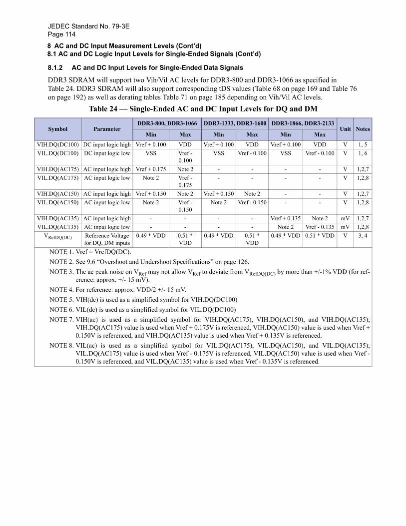
JEDEC Standard No. 79-3EPage 114
es
VIVI
VI 7VI 8
VI 7VI 8
VI 7VI 8
f-
); +
); -
8 AC and DC Input Measurement Levels (Cont’d)8.1 AC and DC Logic Input Levels for Single-Ended Signals (Cont’d)
8.1.2 AC and DC Input Levels for Single-Ended Data Signals
DDR3 SDRAM will support two Vih/Vil AC levels for DDR3-800 and DDR3-1066 as specified in Table 24. DDR3 SDRAM will also support corresponding tDS values (Table 68 on page 169 and Table 76 on page 192) as well as derating tables Table 71 on page 185 depending on Vih/Vil AC levels.
Table 24 — Single-Ended AC and DC Input Levels for DQ and DM
Symbol ParameterDDR3-800, DDR3-1066 DDR3-1333, DDR3-1600 DDR3-1866, DDR3-2133
Unit NotMin Max Min Max Min Max
H.DQ(DC100) DC input logic high Vref + 0.100 VDD Vref + 0.100 VDD Vref + 0.100 VDD V 1, 5L.DQ(DC100) DC input logic low VSS Vref -
0.100VSS Vref - 0.100 VSS Vref - 0.100 V 1, 6
H.DQ(AC175) AC input logic high Vref + 0.175 Note 2 - - - - V 1,2,L.DQ(AC175) AC input logic low Note 2 Vref -
0.175- - - - V 1,2,
H.DQ(AC150) AC input logic high Vref + 0.150 Note 2 Vref + 0.150 Note 2 - - V 1,2,L.DQ(AC150) AC input logic low Note 2 Vref -
0.150Note 2 Vref - 0.150 - - V 1,2,
H.DQ(AC135) AC input logic high - - - - Vref + 0.135 Note 2 mV 1,2,L.DQ(AC135) AC input logic low - - - - Note 2 Vref - 0.135 mV 1,2,VRefDQ(DC) Reference Voltage
for DQ, DM inputs0.49 * VDD 0.51 *
VDD0.49 * VDD 0.51 *
VDD0.49 * VDD 0.51 * VDD V 3, 4
NOTE 1. Vref = VrefDQ(DC).NOTE 2. See 9.6 “Overshoot and Undershoot Specifications” on page 126.NOTE 3. The ac peak noise on VRef may not allow VRef to deviate from VRefDQ(DC) by more than +/-1% VDD (for re
erence: approx. +/- 15 mV).NOTE 4. For reference: approx. VDD/2 +/- 15 mV.NOTE 5. VIH(dc) is used as a simplified symbol for VIH.DQ(DC100)NOTE 6. VIL(dc) is used as a simplified symbol for VIL.DQ(DC100)NOTE 7. VIH(ac) is used as a simplified symbol for VIH.DQ(AC175), VIH.DQ(AC150), and VIH.DQ(AC135
VIH.DQ(AC175) value is used when Vref + 0.175V is referenced, VIH.DQ(AC150) value is used when Vref0.150V is referenced, and VIH.DQ(AC135) value is used when Vref + 0.135V is referenced.
NOTE 8. VIL(ac) is used as a simplified symbol for VIL.DQ(AC175), VIL.DQ(AC150), and VIL.DQ(AC135VIL.DQ(AC175) value is used when Vref - 0.175V is referenced, VIL.DQ(AC150) value is used when Vref0.150V is referenced, and VIL.DQ(AC135) value is used when Vref - 0.135V is referenced.
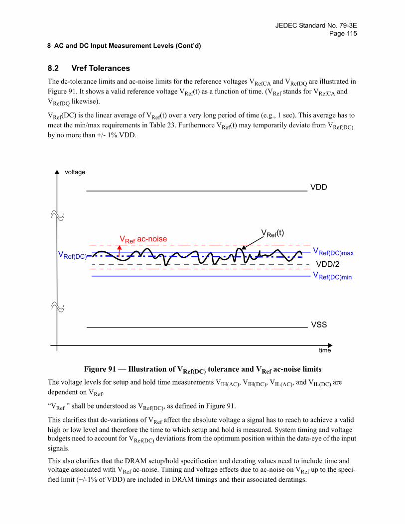
JEDEC Standard No. 79-3EPage 115
8 AC and DC Input Measurement Levels (Cont’d)
8.2 Vref TolerancesThe dc-tolerance limits and ac-noise limits for the reference voltages VRefCA and VRefDQ are illustrated in Figure 91. It shows a valid reference voltage VRef(t) as a function of time. (VRef stands for VRefCA and VRefDQ likewise).
VRef(DC) is the linear average of VRef(t) over a very long period of time (e.g., 1 sec). This average has to meet the min/max requirements in Table 23. Furthermore VRef(t) may temporarily deviate from VRef(DC) by no more than +/- 1% VDD.
Figure 91 — Illustration of VRef(DC) tolerance and VRef ac-noise limitsThe voltage levels for setup and hold time measurements VIH(AC), VIH(DC), VIL(AC), and VIL(DC) are dependent on VRef.
“VRef ” shall be understood as VRef(DC), as defined in Figure 91.
This clarifies that dc-variations of VRef affect the absolute voltage a signal has to reach to achieve a valid high or low level and therefore the time to which setup and hold is measured. System timing and voltage budgets need to account for VRef(DC) deviations from the optimum position within the data-eye of the input signals.
This also clarifies that the DRAM setup/hold specification and derating values need to include time and voltage associated with VRef ac-noise. Timing and voltage effects due to ac-noise on VRef up to the speci-fied limit (+/-1% of VDD) are included in DRAM timings and their associated deratings.
VDD
VSS
VDD/2VRef(DC)
VRef ac-noise
voltage
time
VRef(DC)max
VRef(DC)min
VRef(t)
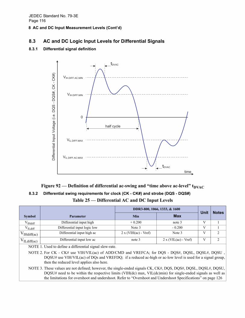
JEDEC Standard No. 79-3EPage 116
Ss
VV
VIHVIL
,p,
U, as6
8 AC and DC Input Measurement Levels (Cont’d)
8.3 AC and DC Logic Input Levels for Differential Signals8.3.1 Differential signal definition
Figure 92 — Definition of differential ac-swing and “time above ac-level” tDVAC8.3.2 Differential swing requirements for clock (CK - CK#) and strobe (DQS - DQS#)
Table 25 — Differential AC and DC Input Levels
ymbol Parameter
DDR3-800, 1066, 1333, & 1600Unit Note
Min Max
IHdiff Differential input high + 0.200 note 3 V 1
ILdiff Differential input logic low Note 3 - 0.200 V 1
diff(ac) Differential input high ac 2 x (VIH(ac) - Vref) Note 3 V 2
diff(ac) Differential input low ac note 3 2 x (VIL(ac) - Vref) V 2
NOTE 1. Used to define a differential signal slew-rate.NOTE 2. For CK - CK# use VIH/VIL(ac) of ADD/CMD and VREFCA; for DQS - DQS#, DQSL, DQSL#, DQSU
DQSU# use VIH/VIL(ac) of DQs and VREFDQ; if a reduced ac-high or ac-low level is used for a signal grouthen the reduced level applies also here.
NOTE 3. These values are not defined; however, the single-ended signals CK, CK#, DQS, DQS#, DQSL, DQSL#, DQSDQSU# need to be within the respective limits (VIH(dc) max, VIL(dc)min) for single-ended signals as wellthe limitations for overshoot and undershoot. Refer to “Overshoot and Undershoot Specifications” on page 12
VIL.DIFF.MAX
0
VIH.DIFF.MIN
VIH.DIFF.AC.MIN
VIL.DIFF.AC.MAX
tDVAC
tDVAC
half cycle
time
Diff
eren
tial I
nput
Vol
tage
(i.e
. DQ
S -
DQ
S#,
CK
- C
K#)
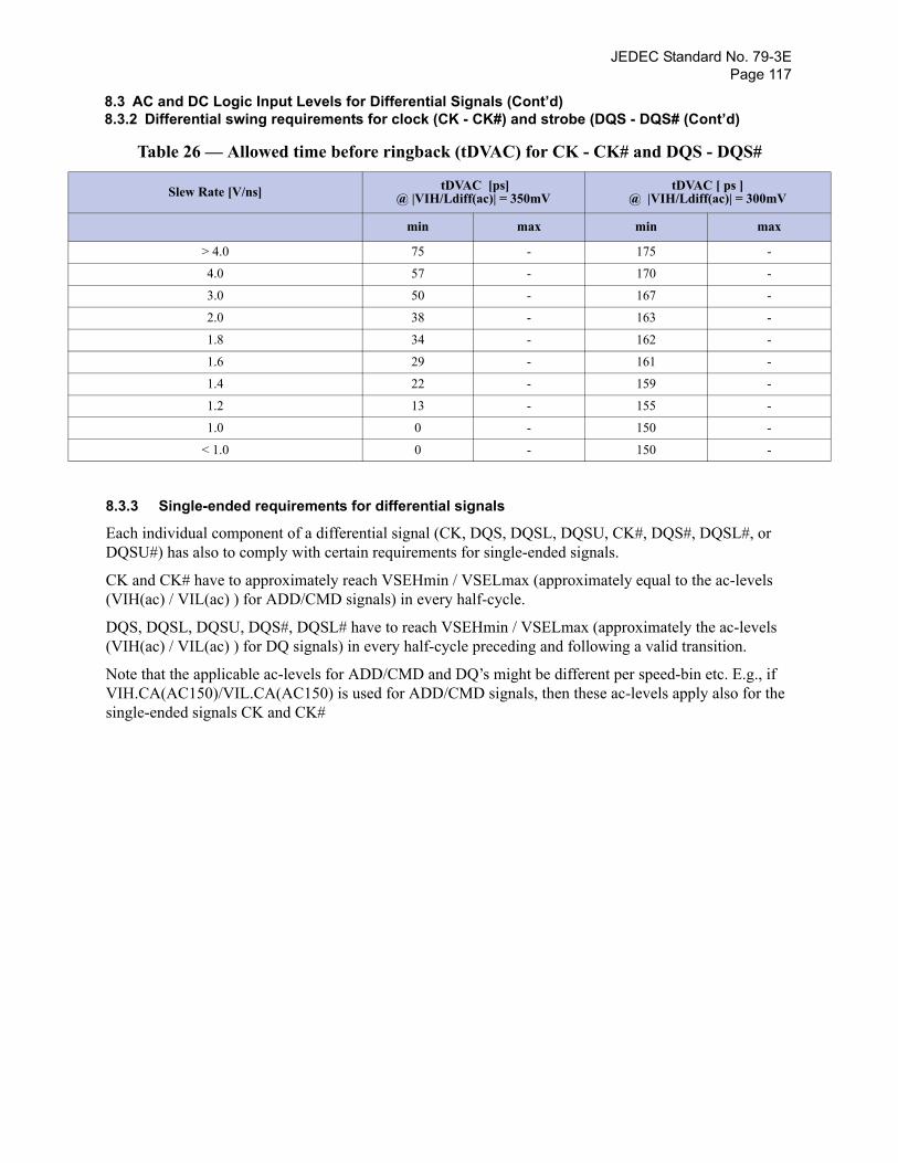
JEDEC Standard No. 79-3EPage 117
8.3 AC and DC Logic Input Levels for Differential Signals (Cont’d)8.3.2 Differential swing requirements for clock (CK - CK#) and strobe (DQS - DQS# (Cont’d)
Table 26 — Allowed time before ringback (tDVAC) for CK - CK# and DQS - DQS#
8.3.3 Single-ended requirements for differential signals
Each individual component of a differential signal (CK, DQS, DQSL, DQSU, CK#, DQS#, DQSL#, or DQSU#) has also to comply with certain requirements for single-ended signals.
CK and CK# have to approximately reach VSEHmin / VSELmax (approximately equal to the ac-levels (VIH(ac) / VIL(ac) ) for ADD/CMD signals) in every half-cycle.
DQS, DQSL, DQSU, DQS#, DQSL# have to reach VSEHmin / VSELmax (approximately the ac-levels (VIH(ac) / VIL(ac) ) for DQ signals) in every half-cycle preceding and following a valid transition.
Note that the applicable ac-levels for ADD/CMD and DQ’s might be different per speed-bin etc. E.g., if VIH.CA(AC150)/VIL.CA(AC150) is used for ADD/CMD signals, then these ac-levels apply also for the single-ended signals CK and CK#
Slew Rate [V/ns] tDVAC [ps]@ |VIH/Ldiff(ac)| = 350mV
tDVAC [ ps ]@ |VIH/Ldiff(ac)| = 300mV
min max min max
> 4.0 75 - 175 -
4.0 57 - 170 -
3.0 50 - 167 -
2.0 38 - 163 -
1.8 34 - 162 -
1.6 29 - 161 -
1.4 22 - 159 -
1.2 13 - 155 -
1.0 0 - 150 -
< 1.0 0 - 150 -

JEDEC Standard No. 79-3EPage 118
e
a
#,sn
8.3 AC and DC Logic Input Levels for Differential Signals (Cont’d)8.3.3 Single-ended requirements for differential signals (Cont’d)
Figure 93 — Single-ended requirement for differential signals.Note that, while ADD/CMD and DQ signal requirements are with respect to Vref, the single-ended compo-nents of differential signals have a requirement with respect to VDD / 2; this is nominally the same. The transition of single-ended signals through the ac-levels is used to measure setup time. For single-ended components of differential signals the requirement to reach VSELmax, VSEHmin has no bearing on tim-ing, but adds a restriction on the common mode characteristics of these signals.
8.4 Differential Input Cross Point VoltageTo guarantee tight setup and hold times as well as output skew parameters with respect to clock and strobe, each cross point voltage of differential input signals (CK, CK# and DQS, DQS#) must meet the require-
Table 27 — Single-ended levels for CK, DQS, DQSL, DQSU, CK#, DQS#, DQSL# or DQSU#
Symbol ParameterDDR3-800, 1066, 1333, & 1600
Unit NotesMin Max
VSEH Single-ended high level for strobes (VDD / 2) + 0.175 note 3 V 1, 2Single-ended high level for CK, CK# (VDD / 2) + 0.175 note 3 V 1, 2
VSEL Single-ended low level for strobes note 3 (VDD / 2) - 0.175 V 1, 2Single-ended low level for CK, CK# note 3 (VDD / 2) - 0.175 V 1, 2
NOTE 1. For CK, CK# use VIH/VIL(ac) of ADD/CMD; for strobes (DQS, DQS#, DQSL, DQSL#, DQSU, DQSU#) usVIH/VIL(ac) of DQs.
NOTE 2. VIH(ac)/VIL(ac) for DQs is based on VREFDQ; VIH(ac)/VIL(ac) for ADD/CMD is based on VREFCA; ifreduced ac-high or ac-low level is used for a signal group, then the reduced level applies also here
NOTE 3. These values are not defined, however the single-ended signals CK, CK#, DQS, DQS#, DQSL, DQSLDQSU, DQSU# need to be within the respective limits (VIH(dc) max, VIL(dc)min) for single-ended signals awell as the limitations for overshoot and undershoot. Refer to “Overshoot and Undershoot Specifications” opage 126
VSS or VSSQ
VDD or VDDQ
VSELmax
VSEHmin
VSEH
VSELtime
VDD/2 or VDDQ/2
CK or DQS
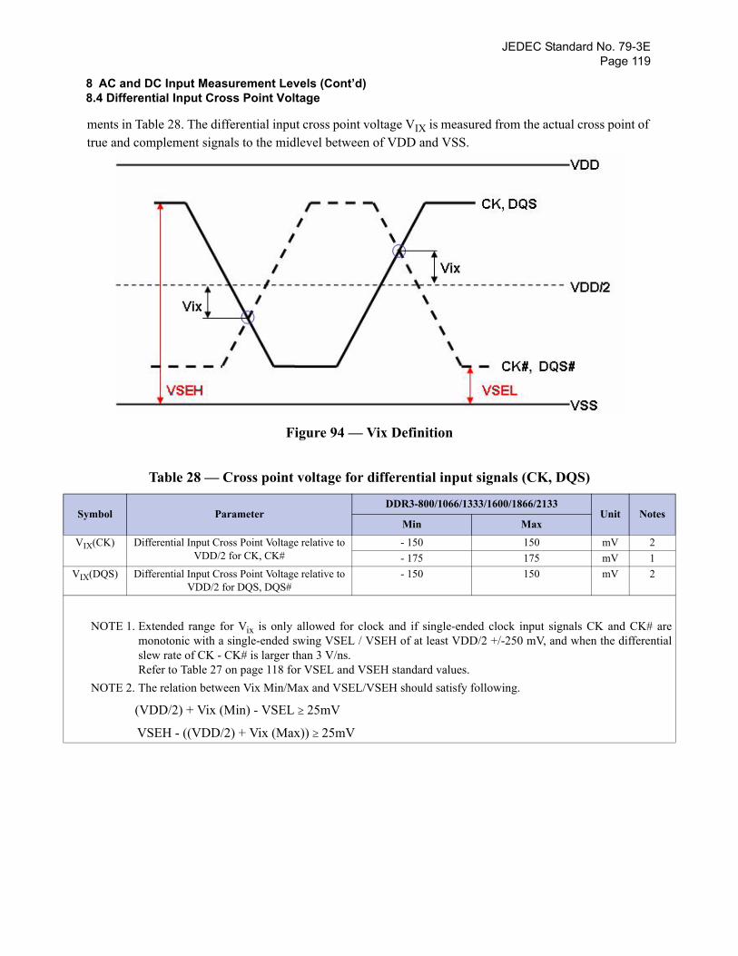
JEDEC Standard No. 79-3EPage 119
V
V
eal
8 AC and DC Input Measurement Levels (Cont’d)8.4 Differential Input Cross Point Voltage
ments in Table 28. The differential input cross point voltage VIX is measured from the actual cross point of true and complement signals to the midlevel between of VDD and VSS.
Figure 94 — Vix Definition
Table 28 — Cross point voltage for differential input signals (CK, DQS)
Symbol ParameterDDR3-800/1066/1333/1600/1866/2133
Unit NotesMin Max
IX(CK) Differential Input Cross Point Voltage relative to VDD/2 for CK, CK#
- 150 150 mV 2- 175 175 mV 1
IX(DQS) Differential Input Cross Point Voltage relative to VDD/2 for DQS, DQS#
- 150 150 mV 2
NOTE 1. Extended range for Vix is only allowed for clock and if single-ended clock input signals CK and CK# armonotonic with a single-ended swing VSEL / VSEH of at least VDD/2 +/-250 mV, and when the differentislew rate of CK - CK# is larger than 3 V/ns. Refer to Table 27 on page 118 for VSEL and VSEH standard values.
NOTE 2. The relation between Vix Min/Max and VSEL/VSEH should satisfy following.
(VDD/2) + Vix (Min) - VSEL ≥ 25mV
VSEH - ((VDD/2) + Vix (Max)) ≥ 25mV
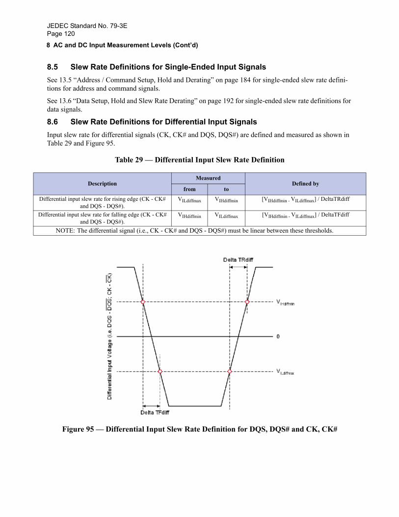
JEDEC Standard No. 79-3EPage 120
D
D
8 AC and DC Input Measurement Levels (Cont’d)
8.5 Slew Rate Definitions for Single-Ended Input SignalsSee 13.5 “Address / Command Setup, Hold and Derating” on page 184 for single-ended slew rate defini-tions for address and command signals.
See 13.6 “Data Setup, Hold and Slew Rate Derating” on page 192 for single-ended slew rate definitions for data signals.
8.6 Slew Rate Definitions for Differential Input SignalsInput slew rate for differential signals (CK, CK# and DQS, DQS#) are defined and measured as shown in Table 29 and Figure 95.
Table 29 — Differential Input Slew Rate Definition
Figure 95 — Differential Input Slew Rate Definition for DQS, DQS# and CK, CK#
DescriptionMeasured
Defined byfrom to
ifferential input slew rate for rising edge (CK - CK# and DQS - DQS#).
VILdiffmax VIHdiffmin [VIHdiffmin - VILdiffmax] / DeltaTRdiff
ifferential input slew rate for falling edge (CK - CK# and DQS - DQS#).
VIHdiffmin VILdiffmax [VIHdiffmin - VILdiffmax] / DeltaTFdiff
NOTE: The differential signal (i.e., CK - CK# and DQS - DQS#) must be linear between these thresholds.

JEDEC Standard No. 79-3EPage 121
Ths page left blank.

JEDEC Standard No. 79-3EPage 122
S s
VVVVV
ng
s
VV
ngial
9 AC and DC Output Measurement Levels (Cont’d)
9 AC and DC Output Measurement Levels
9.1 Single Ended AC and DC Output LevelsTable 30 shows the output levels used for measurements of single ended signals.
Table 30 — Single-ended AC and DC Output Levels
9.2 Differential AC and DC Output LevelsTable 31 shows the output levels used for measurements of differential signals.
Table 31 — Differential AC and DC Output Levels
ymbol Parameter DDR3-800, 1066, 1333, and 1600 Unit Note
OH(DC) DC output high measurement level (for IV curve linearity) 0.8 x VDDQ V
OM(DC) DC output mid measurement level (for IV curve linearity) 0.5 x VDDQ V
OL(DC) DC output low measurement level (for IV curve linearity) 0.2 x VDDQ V
OH(AC) AC output high measurement level (for output SR) VTT + 0.1 x VDDQ V 1
OL(AC) AC output low measurement level (for output SR) VTT - 0.1 x VDDQ V 1NOTE 1. The swing of ± 0.1 × VDDQ is based on approximately 50% of the static single-ended output high or low swi
with a driver impedance of 40 Ω and an effective test load of 25 Ω to VTT = VDDQ/2.
Symbol Parameter DDR3-800, 1066, 1333, and 1600 Unit Note
OHdiff(AC) AC differential output high measurement level (for output SR) + 0.2 x VDDQ V 1
OLdiff(AC) AC differential output low measurement level (for output SR) - 0.2 x VDDQ V 1NOTE 1. The swing of ± 0.2 × VDDQ is based on approximately 50% of the static single-ended output high or low swi
with a driver impedance of 40 Ω and an effective test load of 25 Ω to VTT = VDDQ/2 at each of the differentoutputs.
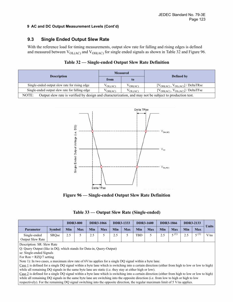
JEDEC Standard No. 79-3EPage 123
N
its
SOu
ns
DesQ: Qse: ForNotCas h) whiCas h) whiresp
9 AC and DC Output Measurement Levels (Cont’d)
9.3 Single Ended Output Slew RateWith the reference load for timing measurements, output slew rate for falling and rising edges is defined and measured between VOL(AC) and VOH(AC) for single ended signals as shown in Table 32 and Figure 96.
Table 32 — Single-ended Output Slew Rate Definition
Figure 96 — Single-ended Output Slew Rate Definition
Table 33 — Output Slew Rate (Single-ended)
DescriptionMeasured
Defined byfrom to
Single-ended output slew rate for rising edge VOL(AC) VOH(AC) [VOH(AC) - VOL(AC)] / DeltaTRseSingle-ended output slew rate for falling edge VOH(AC) VOL(AC) [VOH(AC) - VOL(AC)] / DeltaTFse
OTE: Output slew rate is verified by design and characterization, and may not be subject to production test.
DDR3-800 DDR3-1066 DDR3-1333 DDR3-1600 DDR3-1866 DDR3-2133Un
Parameter Symbol Min Max Min Max Min Max Min Max Min Max Min Max
ingle-ended tput Slew Rate
SRQse 2.5 5 2.5 5 2.5 5 TBD 5 2.5 5 (1) 2.5 5 (1) V/
cription: SR: Slew Rateuery Output (like in DQ, which stands for Data-in, Query-Output)
Single-ended Signals Ron = RZQ/7 settinge 1): In two cases, a maximum slew rate of 6V/ns applies for a single DQ signal within a byte lane.e 1 is defined for a single DQ signal within a byte lane which is switching into a certain direction (either from high to low or low to higle all remaining DQ signals in the same byte lane are static (i.e. they stay at either high or low).e 2 is defined for a single DQ signal within a byte lane which is switching into a certain direction (either from high to low or low to higle all remaining DQ signals in the same byte lane are switching into the opposite direction (i.e. from low to high or high to low ectively). For the remaining DQ signal switching into the opposite direction, the regular maximum limit of 5 V/ns applies.
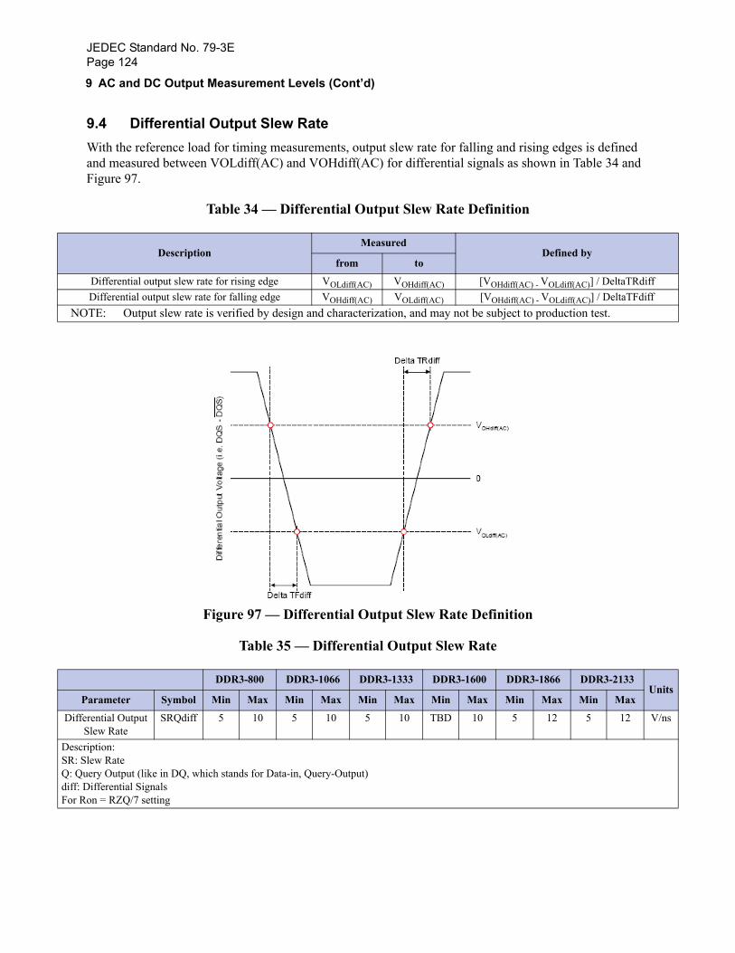
JEDEC Standard No. 79-3EPage 124
N
its
Dif ns
DesSR:Q: QdiffFor
9 AC and DC Output Measurement Levels (Cont’d)
9.4 Differential Output Slew RateWith the reference load for timing measurements, output slew rate for falling and rising edges is defined and measured between VOLdiff(AC) and VOHdiff(AC) for differential signals as shown in Table 34 and Figure 97.
Table 34 — Differential Output Slew Rate Definition
Figure 97 — Differential Output Slew Rate Definition
Table 35 — Differential Output Slew Rate
DescriptionMeasured
Defined byfrom to
Differential output slew rate for rising edge VOLdiff(AC) VOHdiff(AC) [VOHdiff(AC) - VOLdiff(AC)] / DeltaTRdiffDifferential output slew rate for falling edge VOHdiff(AC) VOLdiff(AC) [VOHdiff(AC) - VOLdiff(AC)] / DeltaTFdiff
OTE: Output slew rate is verified by design and characterization, and may not be subject to production test.
DDR3-800 DDR3-1066 DDR3-1333 DDR3-1600 DDR3-1866 DDR3-2133Un
Parameter Symbol Min Max Min Max Min Max Min Max Min Max Min Max
ferential Output Slew Rate
SRQdiff 5 10 5 10 5 10 TBD 10 5 12 5 12 V/
cription: Slew Rateuery Output (like in DQ, which stands for Data-in, Query-Output)
: Differential Signals Ron = RZQ/7 setting
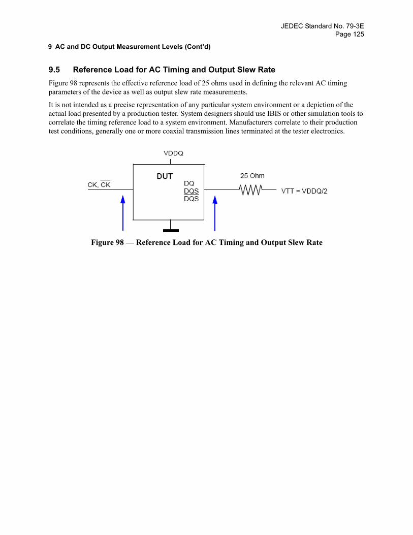
JEDEC Standard No. 79-3EPage 125
9 AC and DC Output Measurement Levels (Cont’d)
9.5 Reference Load for AC Timing and Output Slew RateFigure 98 represents the effective reference load of 25 ohms used in defining the relevant AC timing parameters of the device as well as output slew rate measurements.
It is not intended as a precise representation of any particular system environment or a depiction of the actual load presented by a production tester. System designers should use IBIS or other simulation tools to correlate the timing reference load to a system environment. Manufacturers correlate to their production test conditions, generally one or more coaxial transmission lines terminated at the tester electronics.
Figure 98 — Reference Load for AC Timing and Output Slew Rate
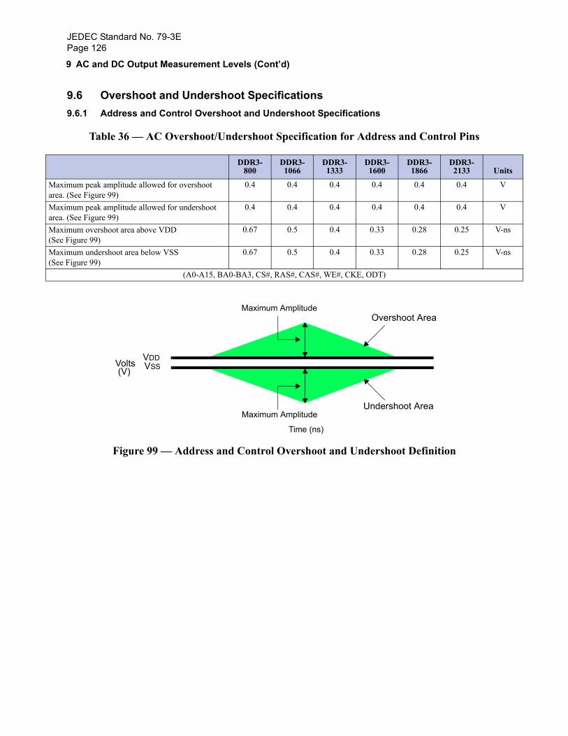
JEDEC Standard No. 79-3EPage 126
MaareMaareMa(SeMa(Se
9 AC and DC Output Measurement Levels (Cont’d)
9.6 Overshoot and Undershoot Specifications9.6.1 Address and Control Overshoot and Undershoot Specifications
Table 36 — AC Overshoot/Undershoot Specification for Address and Control Pins
Figure 99 — Address and Control Overshoot and Undershoot Definition
DDR3-800
DDR3-1066
DDR3-1333
DDR3-1600
DDR3-1866
DDR3-2133 Units
ximum peak amplitude allowed for overshoot a. (See Figure 99)
0.4 0.4 0.4 0.4 0.4 0.4 V
ximum peak amplitude allowed for undershoot a. (See Figure 99)
0.4 0.4 0.4 0.4 0.4 0.4 V
ximum overshoot area above VDDe Figure 99)
0.67 0.5 0.4 0.33 0.28 0.25 V-ns
ximum undershoot area below VSSe Figure 99)
0.67 0.5 0.4 0.33 0.28 0.25 V-ns
(A0-A15, BA0-BA3, CS#, RAS#, CAS#, WE#, CKE, ODT)
Overshoot AreaMaximum Amplitude
VDD
Undershoot AreaMaximum Amplitude
VSSVolts(V)
Time (ns)
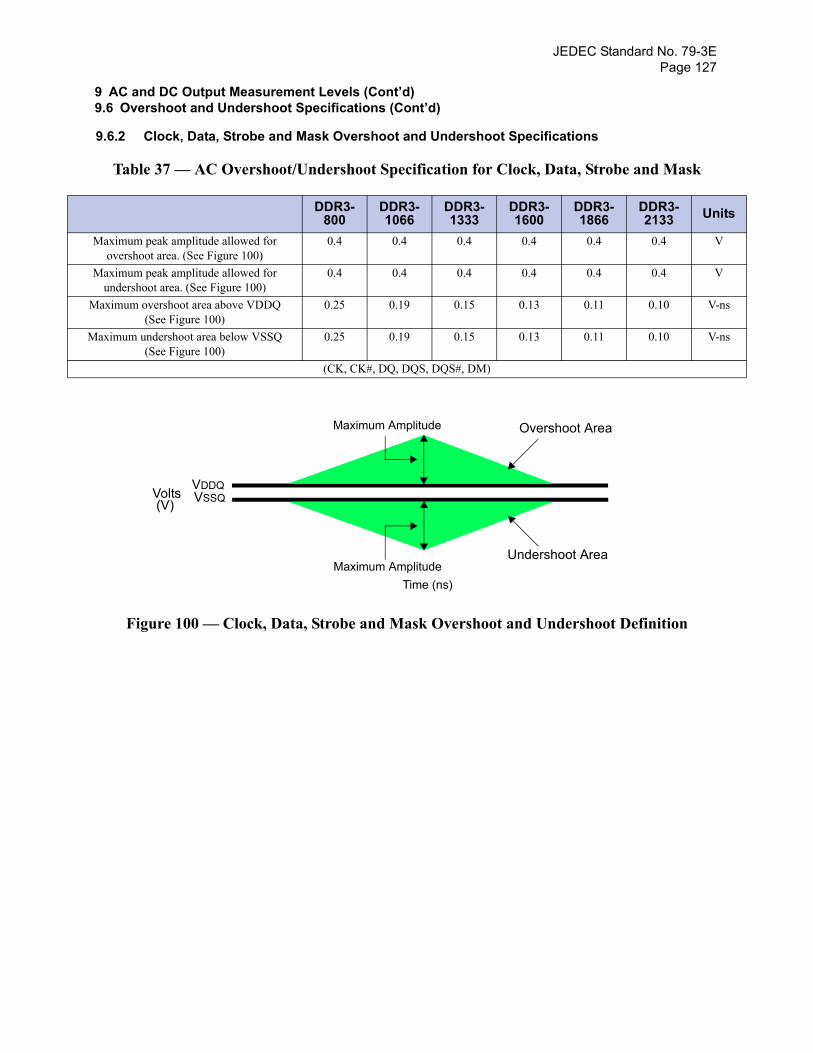
JEDEC Standard No. 79-3EPage 127
9 AC and DC Output Measurement Levels (Cont’d)9.6 Overshoot and Undershoot Specifications (Cont’d)
9.6.2 Clock, Data, Strobe and Mask Overshoot and Undershoot Specifications
Table 37 — AC Overshoot/Undershoot Specification for Clock, Data, Strobe and Mask
Figure 100 — Clock, Data, Strobe and Mask Overshoot and Undershoot Definition
DDR3-800
DDR3-1066
DDR3-1333
DDR3-1600
DDR3-1866
DDR3-2133 Units
Maximum peak amplitude allowed for overshoot area. (See Figure 100)
0.4 0.4 0.4 0.4 0.4 0.4 V
Maximum peak amplitude allowed for undershoot area. (See Figure 100)
0.4 0.4 0.4 0.4 0.4 0.4 V
Maximum overshoot area above VDDQ (See Figure 100)
0.25 0.19 0.15 0.13 0.11 0.10 V-ns
Maximum undershoot area below VSSQ (See Figure 100)
0.25 0.19 0.15 0.13 0.11 0.10 V-ns
(CK, CK#, DQ, DQS, DQS#, DM)
Overshoot AreaMaximum Amplitude
VDDQ
Undershoot AreaMaximum Amplitude
VSSQVolts(V)
Time (ns)
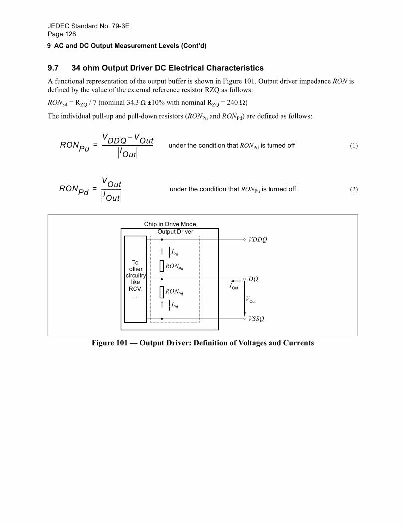
JEDEC Standard No. 79-3EPage 128
9 AC and DC Output Measurement Levels (Cont’d)
9.7 34 ohm Output Driver DC Electrical CharacteristicsA functional representation of the output buffer is shown in Figure 101. Output driver impedance RON is defined by the value of the external reference resistor RZQ as follows:
RON34 = RZQ / 7 (nominal 34.3 Ω ±10% with nominal RZQ = 240 Ω)
The individual pull-up and pull-down resistors (RONPu and RONPd) are defined as follows:
under the condition that RONPd is turned off (1)
under the condition that RONPu is turned off (2)
Figure 101 — Output Driver: Definition of Voltages and Currents
RONPuVDDQ VOut–
IOut--------------------------------------=
RONPdVOutIOut---------------=
VDDQ
VSSQ
Chip in Drive Mode
DQ
VOut
IOut
RONPu
RONPd
Output Driver
Toother
circuitrylike
RCV,...
IPu
IPd

JEDEC Standard No. 79-3EPage 129
T
MisMM
9 AC and DC Output Measurement Levels (Cont’d)9.7 34 ohm Output Driver DC Electrical Characteristics (Cont’d)
NOTE 1. The tolerance limits are specified after calibration with stable voltage and temperature. For the behav-ior of the tolerance limits if temperature or voltage changes after calibration, see following section onvoltage and temperature sensitivity.
NOTE 2. The tolerance limits are specified under the condition that VDDQ = VDD and that VSSQ = VSS.NOTE 3. Pull-down and pull-up output driver impedances are recommended to be calibrated at 0.5 × VDDQ.
Other calibration schemes may be used to achieve the linearity spec shown above, e.g. calibration at0.2 × VDDQ and 0.8 × VDDQ.
NOTE 4. Measurement definition for mismatch between pull-up and pull-down, MMPuPd:Measure RONPu and RONPd, both at 0.5 * VDDQ:
9.7.1 Output Driver Temperature and Voltage sensitivity
If temperature and/or voltage change after calibration, the tolerance limits widen according to Table 39 and Table 40.
ΔT = T - T(@calibration); ΔV= VDDQ - VDDQ(@calibration); VDD = VDDQ
NOTE: dRONdT and dRONdV are not subject to production test but are verified by design and characterization.
able 38 — Output Driver DC Electrical Characteristics, assuming RZQ = 240 Ω ; entire operatingtemperature range; after proper ZQ calibration
RONNom Resistor VOut min nom max Unit Notes
34 Ω RON34Pd VOLdc = 0.2 × VDDQ 0.6 1.0 1.1 RZQ/7 1, 2, 3VOMdc = 0.5 × VDDQ 0.9 1.0 1.1 RZQ/7 1, 2, 3VOHdc = 0.8 × VDDQ 0.9 1.0 1.4 RZQ/7 1, 2, 3
RON34Pu VOLdc = 0.2 × VDDQ 0.9 1.0 1.4 RZQ/7 1, 2, 3VOMdc = 0.5 × VDDQ 0.9 1.0 1.1 RZQ/7 1, 2, 3VOHdc = 0.8 × VDDQ 0.6 1.0 1.1 RZQ/7 1, 2, 3
40 Ω RON40Pd VOLdc = 0.2 × VDDQ 0.6 1.0 1.1 RZQ/6 1, 2, 3VOMdc = 0.5 × VDDQ 0.9 1.0 1.1 RZQ/6 1, 2, 3VOHdc = 0.8 × VDDQ 0.9 1.0 1.4 RZQ/6 1, 2, 3
RON40Pu VOLdc = 0.2 × VDDQ 0.9 1.0 1.4 RZQ/6 1, 2, 3VOMdc = 0.5 × VDDQ 0.9 1.0 1.1 RZQ/6 1, 2, 3VOHdc = 0.8 × VDDQ 0.6 1.0 1.1 RZQ/6 1, 2, 3
match between pull-up and pull-down, PuPd
VOMdc 0.5 × VDDQ
-10 +10 % 1, 2, 4
MMPuPdRONPu RONPd–
RONNom-------------------------------------------------x100=
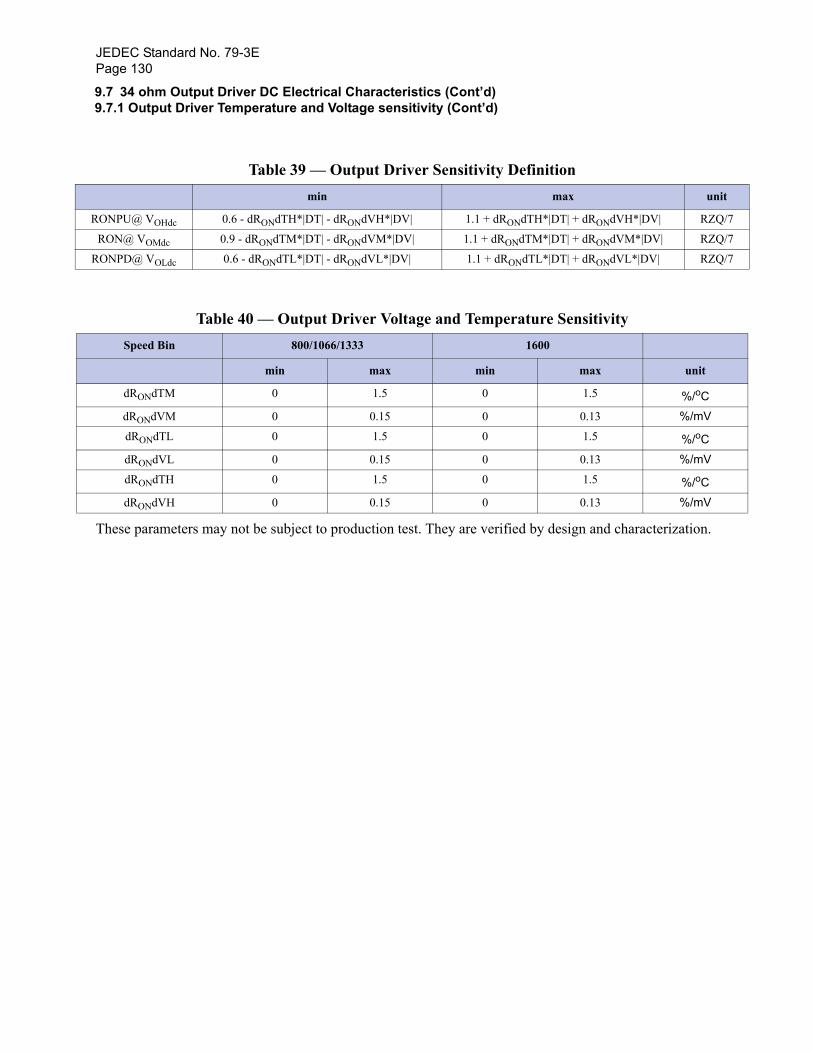
JEDEC Standard No. 79-3EPage 130
9.7 34 ohm Output Driver DC Electrical Characteristics (Cont’d)9.7.1 Output Driver Temperature and Voltage sensitivity (Cont’d)
These parameters may not be subject to production test. They are verified by design and characterization.
Table 39 — Output Driver Sensitivity Definitionmin max unit
RONPU@ VOHdc 0.6 - dRONdTH*|DT| - dRONdVH*|DV| 1.1 + dRONdTH*|DT| + dRONdVH*|DV| RZQ/7
RON@ VOMdc 0.9 - dRONdTM*|DT| - dRONdVM*|DV| 1.1 + dRONdTM*|DT| + dRONdVM*|DV| RZQ/7
RONPD@ VOLdc 0.6 - dRONdTL*|DT| - dRONdVL*|DV| 1.1 + dRONdTL*|DT| + dRONdVL*|DV| RZQ/7
Table 40 — Output Driver Voltage and Temperature SensitivitySpeed Bin 800/1066/1333 1600
min max min max unit
dRONdTM 0 1.5 0 1.5 %/oC
dRONdVM 0 0.15 0 0.13 %/mV
dRONdTL 0 1.5 0 1.5 %/oC
dRONdVL 0 0.15 0 0.13 %/mV
dRONdTH 0 1.5 0 1.5 %/oC
dRONdVH 0 0.15 0 0.13 %/mV
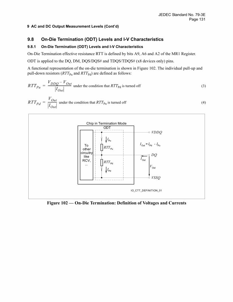
JEDEC Standard No. 79-3EPage 131
9 AC and DC Output Measurement Levels (Cont’d)
9.8 On-Die Termination (ODT) Levels and I-V Characteristics9.8.1 On-Die Termination (ODT) Levels and I-V Characteristics
On-Die Termination effective resistance RTT is defined by bits A9, A6 and A2 of the MR1 Register.
ODT is applied to the DQ, DM, DQS/DQS# and TDQS/TDQS# (x8 devices only) pins.
A functional representation of the on-die termination is shown in Figure 102. The individual pull-up and pull-down resistors (RTTPu and RTTPd) are defined as follows:
under the condition that RTTPd is turned off (3)
under the condition that RTTPu is turned off (4)
Figure 102 — On-Die Termination: Definition of Voltages and Currents
RTTPuVDDQ VOut–
IOut-------------------------------=
RTTPdVOutIOut------------=
IO_CTT_DEFINITION_01
VDDQ
VSSQ
Chip in Termination Mode
DQ
VOut
IOut
RTTPu
RTTPd
ODT
Toother
circuitrylike
RCV,...
IPu
IPd
IOut = IPd - IPu

JEDEC Standard No. 79-3EPage 132
,
,,
,
,,
,
,,
,
,,
9 AC and DC Output Measurement Levels (Cont’d)9.8 On-Die Termination (ODT) Levels and I-V Characteristics (Cont’d)
9.8.2 ODT DC Electrical Characteristics
Table 41 provides an overview of the ODT DC electrical characteristics. The values for RTT60Pd120, RTT60Pu120, RTT120Pd240, RTT120Pu240, RTT40Pd80, RTT40Pu80, RTT30Pd60, RTT30Pu60 , RTT20Pd40, RTT20Pu40 are not specification requirements, but can be used as design guide lines:
Table 41 — ODT DC Electrical Characteristics, assuming RZQ = 240 Ω +/- 1% entire operating temperature range; after proper ZQ calibration
MR1 A9, A6, A2 RTT Resistor VOut min nom max Unit Notes
0, 1, 0 120 Ω RTT120Pd240 VOLdc 0.2 × VDDQ
0.6 1.00 1.1 RZQ 1, 2, 3, 4
0.5 × VDDQ 0.9 1.00 1.1 RZQ 1, 2, 3, 4VOHdc
0.8 × VDDQ 0.9 1.00 1.4 RZQ 1, 2, 3, 4
RTT120Pu240 VOLdc 0.2 × VDDQ
0.9 1.00 1.4 RZQ 1, 2, 3, 4
0.5 × VDDQ 0.9 1.00 1.1 RZQ 1, 2, 3, 4VOHdc
0.8 × VDDQ 0.6 1.00 1.1 RZQ 1, 2, 3, 4
RTT120 VIL(ac) to VIH(ac) 0.9 1.00 1.6 RZQ/2 1, 2, 5,0, 0, 1 60 Ω RTT60Pd120 VOLdc
0.2 × VDDQ 0.6 1.00 1.1 RZQ/2 1, 2, 3, 4
0.5 × VDDQ 0.9 1.00 1.1 RZQ/2 1, 2, 3, 4VOHdc
0.8 × VDDQ 0.9 1.00 1.4 RZQ/2 1, 2, 3, 4
RTT60Pu120 VOLdc 0.2 × VDDQ
0.9 1.00 1.4 RZQ/2 1, 2, 3, 4
0.5 × VDDQ 0.9 1.00 1.1 RZQ/2 1, 2, 3, 4VOHdc
0.8 × VDDQ 0.6 1.00 1.1 RZQ/2 1, 2, 3, 4
RTT60 VIL(ac) to VIH(ac) 0.9 1.00 1.6 RZQ/4 1, 2, 5,

JEDEC Standard No. 79-3EPage 133
,
,,
,
,,
,
,,
,
,,
,
,,
,
,,
,
9.8 On-Die Termination (ODT) Levels and I-V Characteristics (Cont’d)9.8.2 ODT DC Electrical Characteristics (Cont’d)
NOTE 1. The tolerance limits are specified after calibration with stable voltage and temperature. For the behav-ior of the tolerance limits if temperature or voltage changes after calibration, see following section onvoltage and temperature sensitivity.
NOTE 2. The tolerance limits are specified under the condition that VDDQ = VDD and that VSSQ = VSS.NOTE 3. Pull-down and pull-up ODT resistors are recommended to be calibrated at 0.5 × VDDQ. Other calibra-
tion schemes may be used to achieve the linearity spec shown above, e.g. calibration at 0.2 × VDDQand 0.8 × VDDQ.
NOTE 4. Not a specification requirement, but a design guide line.
0, 1, 1 40 Ω RTT40Pd80 VOLdc 0.2 × VDDQ
0.6 1.00 1.1 RZQ/3 1, 2, 3, 4
0.5 × VDDQ 0.9 1.00 1.1 RZQ/3 1, 2, 3, 4VOHdc
0.8 × VDDQ 0.9 1.00 1.4 RZQ/3 1, 2, 3, 4
RTT40Pu80 VOLdc 0.2 × VDDQ
0.9 1.00 1.4 RZQ/3 1, 2, 3, 4
0.5 × VDDQ 0.9 1.00 1.1 RZQ/3 1, 2, 3, 4VOHdc
0.8 × VDDQ 0.6 1.00 1.1 RZQ/3 1, 2, 3, 4
RTT40 VIL(ac) to VIH(ac) 0.9 1.00 1.6 RZQ/6 1, 2, 5,1, 0, 1 30 Ω RTT30Pd60 VOLdc
0.2 × VDDQ 0.6 1.00 1.1 RZQ/4 1, 2, 3, 4
0.5 × VDDQ 0.9 1.00 1.1 RZQ/4 1, 2, 3, 4VOHdc
0.8 × VDDQ 0.9 1.00 1.4 RZQ/4 1, 2, 3, 4
RTT30Pu60 VOLdc 0.2 × VDDQ
0.9 1.00 1.4 RZQ/4 1, 2, 3, 4
0.5 × VDDQ 0.9 1.00 1.1 RZQ/4 1, 2, 3, 4VOHdc
0.8 × VDDQ 0.6 1.00 1.1 RZQ/4 1, 2, 3, 4
RTT30 VIL(ac) to VIH(ac) 0.9 1.00 1.6 RZQ/8 1, 2, 5,1, 0, 0 20 Ω RTT20Pd40 VOLdc
0.2 × VDDQ 0.6 1.00 1.1 RZQ/6 1, 2, 3, 4
0.5 × VDDQ 0.9 1.00 1.1 RZQ/6 1, 2, 3, 4VOHdc
0.8 × VDDQ 0.9 1.00 1.4 RZQ/6 1, 2, 3, 4
RTT20Pu40 VOLdc 0.2 × VDDQ
0.9 1.00 1.4 RZQ/6 1, 2, 3, 4
0.5 × VDDQ 0.9 1.00 1.1 RZQ/6 1, 2, 3, 4VOHdc
0.8 × VDDQ 0.6 1.00 1.1 RZQ/6 1, 2, 3, 4
RTT20 VIL(ac) to VIH(ac) 0.9 1.00 1.6 RZQ/12 1, 2, 5,Deviation of VM w.r.t. VDDQ/2, DVM -5 +5 % 1, 2, 5, 6
Table 41 — ODT DC Electrical Characteristics, assuming RZQ = 240 Ω +/- 1% entire operating temperature range; after proper ZQ calibration (Cont’d)
MR1 A9, A6, A2 RTT Resistor VOut min nom max Unit Notes

JEDEC Standard No. 79-3EPage 134
9.8 On-Die Termination (ODT) Levels and I-V Characteristics (Cont’d)9.8.2 ODT DC Electrical Characteristics (Cont’d)
NOTE 5. Measurement definition for RTT: Apply VIH(ac) to pin under test and measure current I(VIH(ac)), then apply VIL(ac) to pin under test andmeasure current I(VIL(ac)) respectively.
NOTE 6. Measurement definition for VM and DVM:Measure voltage (VM) at test pin (midpoint) with no load:
RTT VIH(ac) VIL(ac)–I(VIH(ac)) I(VIL(ac))–---------------------------------------------------------=
VMΔ 2 VM×VDDQ------------------ 1–⎝ ⎠
⎛ ⎞ 100×=
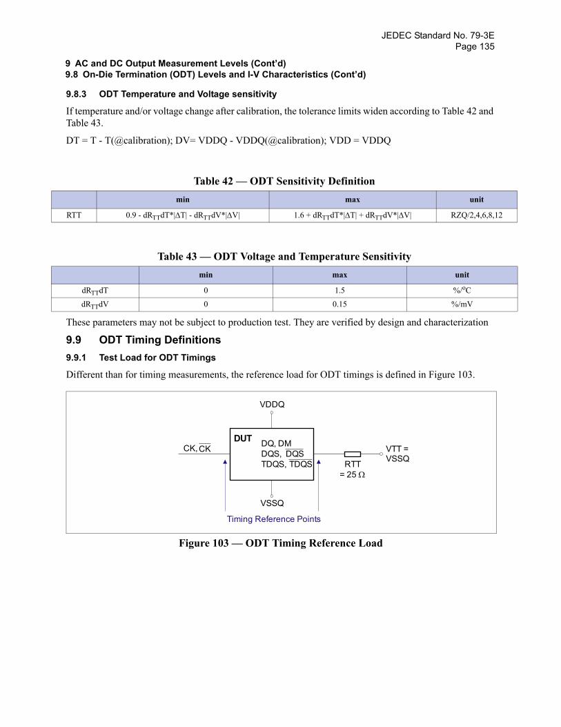
JEDEC Standard No. 79-3EPage 135
9 AC and DC Output Measurement Levels (Cont’d)9.8 On-Die Termination (ODT) Levels and I-V Characteristics (Cont’d)
9.8.3 ODT Temperature and Voltage sensitivity
If temperature and/or voltage change after calibration, the tolerance limits widen according to Table 42 and Table 43.
DT = T - T(@calibration); DV= VDDQ - VDDQ(@calibration); VDD = VDDQ
These parameters may not be subject to production test. They are verified by design and characterization
9.9 ODT Timing Definitions9.9.1 Test Load for ODT Timings
Different than for timing measurements, the reference load for ODT timings is defined in Figure 103.
Figure 103 — ODT Timing Reference Load
Table 42 — ODT Sensitivity Definitionmin max unit
RTT 0.9 - dRTTdT*|ΔT| - dRTTdV*|ΔV| 1.6 + dRTTdT*|ΔT| + dRTTdV*|ΔV| RZQ/2,4,6,8,12
Table 43 — ODT Voltage and Temperature Sensitivitymin max unit
dRTTdT 0 1.5 %/oC
dRTTdV 0 0.15 %/mV
BD_REFLOAD_ODT
CKCK,
VDDQ
DQSDQS,TDQSTDQS,
DQ, DMDUTVTT =VSSQRTT
= 25 Ω
VSSQ
Timing Reference Points

JEDEC Standard No. 79-3EPage 136
Sy
t
tA
t
tA
t
Me
9 AC and DC Output Measurement Levels (Cont’d)9.9 ODT Timing Definitions (Cont’d)
9.9.2 ODT Timing Definitions
Definitions for tAON, tAONPD, tAOF, tAOFPD and tADC are provided in Table 44 and subsequent figures. Mea-surement reference settings are provided in Table 45.
Table 44 — ODT Timing Definitions mbol Begin Point Definition End Point Definition Figure
AON Rising edge of CK - CK# defined by the end point of ODTLon
Extrapolated point at VSSQ Figure 104
ONPD Rising edge of CK - CK# with ODT being first registered high
Extrapolated point at VSSQ Figure 105
AOF Rising edge of CK - CK#defined by the end point of ODTLoff
End point: Extrapolated point at VRTT_Nom Figure 106
OFPD Rising edge of CK - CK# with ODT being first registered low
End point: Extrapolated point at VRTT_Nom Figure 107
ADC Rising edge of CK - CK# defined by the end point of ODTLcnw, ODTLcwn4 or ODTLcwn8
End point: Extrapolated point at VRTT_Wr and VRTT_Nom respectively
Figure 108
Table 45 — Reference Settings for ODT Timing Measurements asured Parameter RTT_Nom Setting RTT_Wr Setting VSW1 [V] VSW2 [V] Note
tAON RZQ/4 NA 0.05 0.10RZQ/12 NA 0.10 0.20
tAONPD RZQ/4 NA 0.05 0.10RZQ/12 NA 0.10 0.20
tAOF RZQ/4 NA 0.05 0.10RZQ/12 NA 0.10 0.20
tAOFPD RZQ/4 NA 0.05 0.10RZQ/12 NA 0.10 0.20
tADC RZQ/12 RZQ/2 0.20 0.30
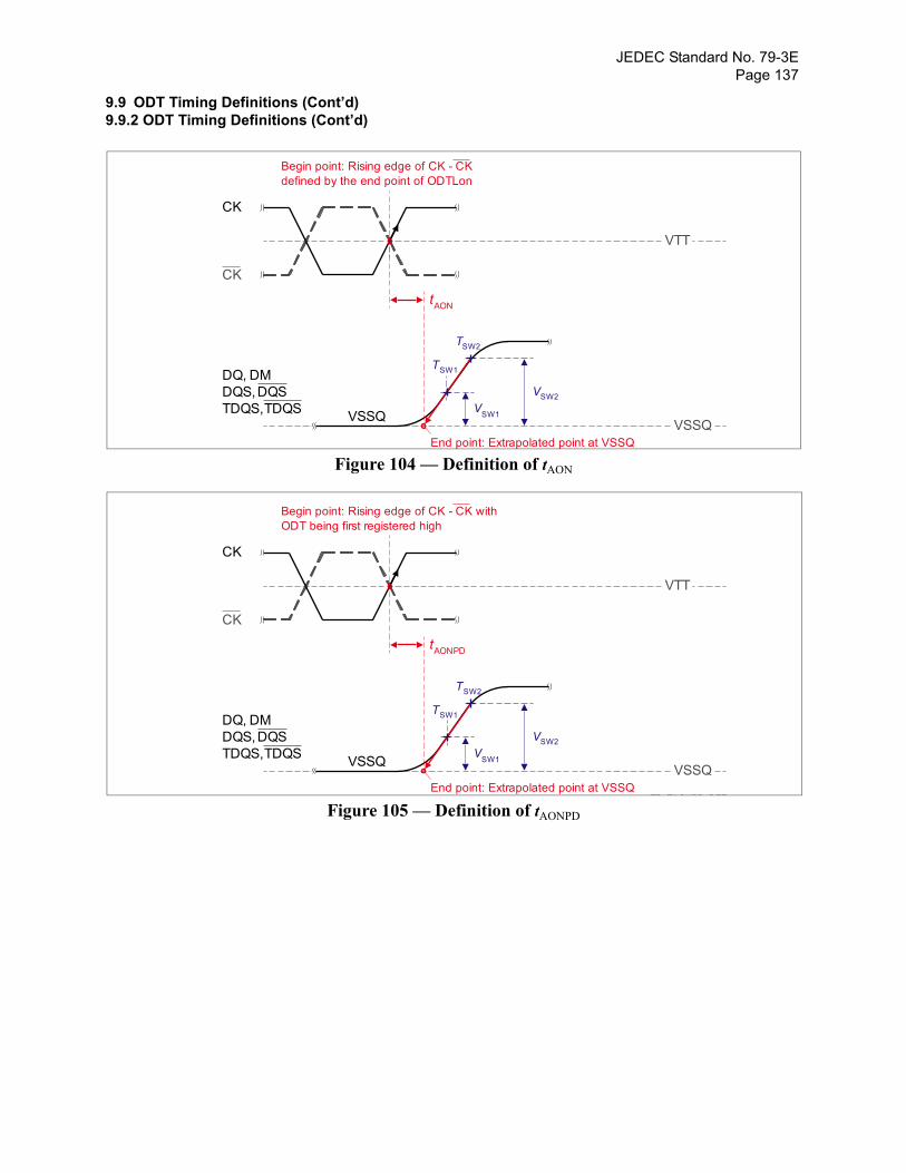
JEDEC Standard No. 79-3EPage 137
9.9 ODT Timing Definitions (Cont’d)9.9.2 ODT Timing Definitions (Cont’d)
Figure 104 — Definition of tAON
Figure 105 — Definition of tAONPD
CK
CK
VTT
tAON
VSSQ
DQSDQ, DM
VSSQ
DQS,TDQSTDQS,
Begin point: Rising edge of CK - CKdefined by the end point of ODTLon
VSW1
VSW2
End point: Extrapolated point at VSSQ
TSW1
TSW2
CK
CK
VTT
TD TAONPD DEF
tAONPD
VSSQ
DQSDQ, DM
VSSQ
DQS,TDQSTDQS,
Begin point: Rising edge of CK - CK withODT being first registered high
VSW1
VSW2
End point: Extrapolated point at VSSQ
TSW1
TSW2

JEDEC Standard No. 79-3EPage 138
9.9 ODT Timing Definitions (Cont’d)9.9.2 ODT Timing Definitions (Cont’d)
Figure 106 — Definition of tAOF
Figure 107 — Definition of tAOFPD
CK
CK
VTT
tAOF
DQSDQ, DMDQS,
TDQSTDQS,
Begin point: Rising edge of CK - CKdefined by the end point of ODTLoff
End point: Extrapolated point at VRTT_NomVRTT_Nom
VSSQVSW1
VSW2
TSW1
TSW2
CK
CK
VTT
tAOFPD
DQSDQ, DMDQS,
TDQSTDQS,
Begin point: Rising edge of CK - CK withODT being first registered low
End point: Extrapolated point at VRTT_NomVRTT_Nom
VSSQVSW1
VSW2
TSW1
TSW2
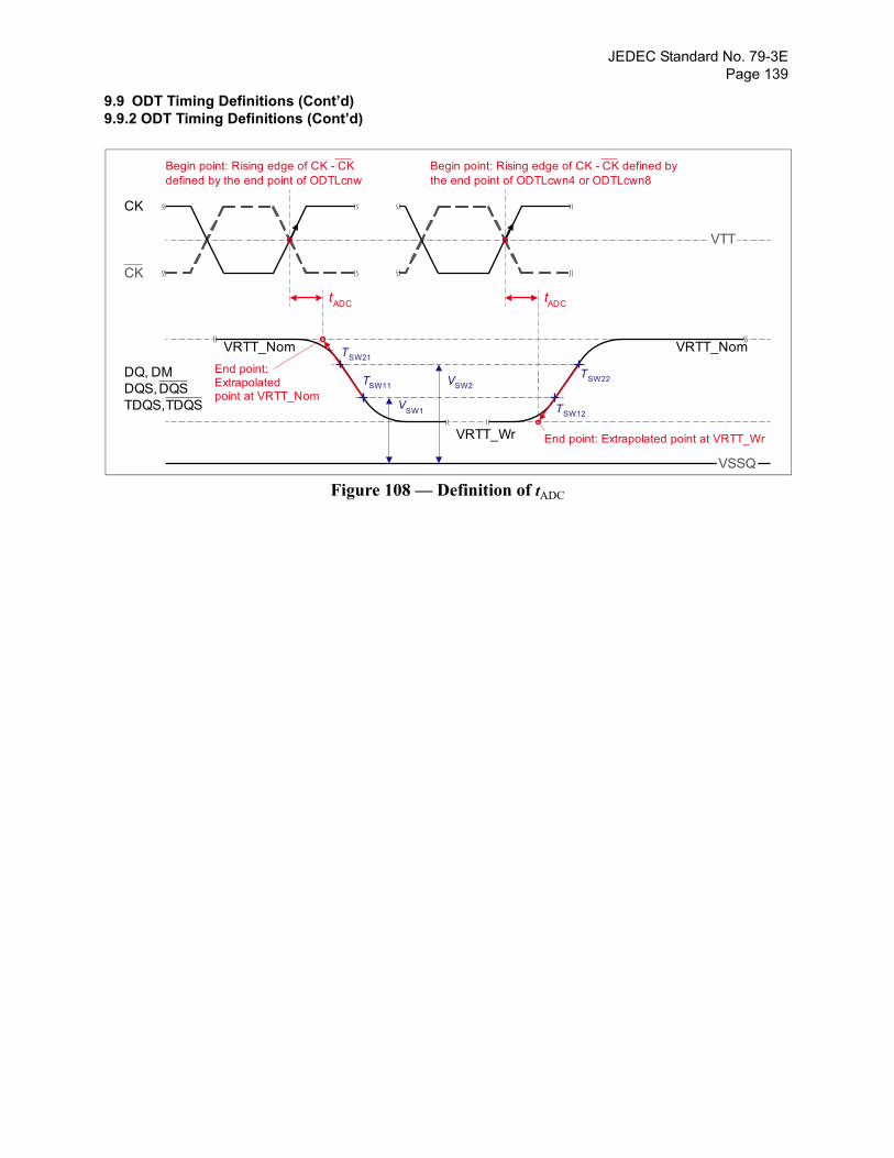
JEDEC Standard No. 79-3EPage 139
9.9 ODT Timing Definitions (Cont’d)9.9.2 ODT Timing Definitions (Cont’d)
Figure 108 — Definition of tADC
CK
CK
tADC
DQSDQ, DMDQS,
TDQSTDQS, VSW1
VSW2
End point:Extrapolatedpoint at VRTT_Nom
TSW11
TSW21
tADC
End point: Extrapolated point at VRTT_Wr
VTT
VSSQ
VRTT_Nom
VRTT_Wr
VRTT_Nom
TSW12
TSW22
Begin point: Rising edge of CK - CKdefined by the end point of ODTLcnw
Begin point: Rising edge of CK - CK defined bythe end point of ODTLcwn4 or ODTLcwn8
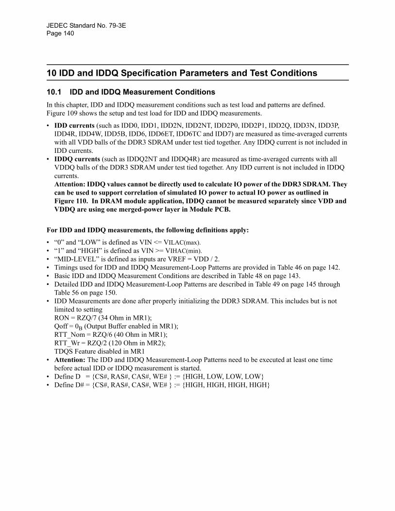
JEDEC Standard No. 79-3EPage 140
10 IDD and IDDQ Specification Parameters and Test Conditions
10.1 IDD and IDDQ Measurement ConditionsIn this chapter, IDD and IDDQ measurement conditions such as test load and patterns are defined. Figure 109 shows the setup and test load for IDD and IDDQ measurements.
• IDD currents (such as IDD0, IDD1, IDD2N, IDD2NT, IDD2P0, IDD2P1, IDD2Q, IDD3N, IDD3P, IDD4R, IDD4W, IDD5B, IDD6, IDD6ET, IDD6TC and IDD7) are measured as time-averaged currents with all VDD balls of the DDR3 SDRAM under test tied together. Any IDDQ current is not included in IDD currents.
• IDDQ currents (such as IDDQ2NT and IDDQ4R) are measured as time-averaged currents with all VDDQ balls of the DDR3 SDRAM under test tied together. Any IDD current is not included in IDDQ currents.Attention: IDDQ values cannot be directly used to calculate IO power of the DDR3 SDRAM. They can be used to support correlation of simulated IO power to actual IO power as outlined in Figure 110. In DRAM module application, IDDQ cannot be measured separately since VDD and VDDQ are using one merged-power layer in Module PCB.
For IDD and IDDQ measurements, the following definitions apply:
• “0” and “LOW” is defined as VIN <= VILAC(max).• “1” and “HIGH” is defined as VIN >= VIHAC(min).• “MID-LEVEL” is defined as inputs are VREF = VDD / 2.• Timings used for IDD and IDDQ Measurement-Loop Patterns are provided in Table 46 on page 142.• Basic IDD and IDDQ Measurement Conditions are described in Table 48 on page 143.• Detailed IDD and IDDQ Measurement-Loop Patterns are described in Table 49 on page 145 through
Table 56 on page 150.• IDD Measurements are done after properly initializing the DDR3 SDRAM. This includes but is not
limited to setting RON = RZQ/7 (34 Ohm in MR1); Qoff = 0B (Output Buffer enabled in MR1); RTT_Nom = RZQ/6 (40 Ohm in MR1); RTT_Wr = RZQ/2 (120 Ohm in MR2);TDQS Feature disabled in MR1
• Attention: The IDD and IDDQ Measurement-Loop Patterns need to be executed at least one time before actual IDD or IDDQ measurement is started.
• Define D = {CS#, RAS#, CAS#, WE# } := {HIGH, LOW, LOW, LOW}• Define D# = {CS#, RAS#, CAS#, WE# } := {HIGH, HIGH, HIGH, HIGH}

JEDEC Standard No. 79-3EPage 141
10 IDD and IDDQ Specification Parameters and Test Conditions (Cont’d)10.1 IDD and IDDQ Measurement Conditions (Cont’d)
Figure 109 — Measurement Setup and Test Load for IDD and IDDQ (optional) Measurements
Figure 110 — Correlation from simulated Channel IO Power to actual Channel IO Power supported by IDDQ Measurement.
IDD
CK/CK#
CS#CKE
ODT
VDD VDDQ
VSS VSSQ
RESET#
RAS#, CAS#, WE#
ZQ
A, BA
IDDQ
DQS, DQS#,DQ, DM,
TDQS, TDQS#VDDQ / 2
RTT = 25 Ω
DDR3SDRAM
(optional)
NOTE: DIMM level Output test load conditionmay be different from above.
Application spec ific memory channel
env ironment
Channel IO Power Simulation
IDDQ Test Load
IDDQSimulation
IDDQ Measurement
Correlation
Correction
Channel IO Power Number
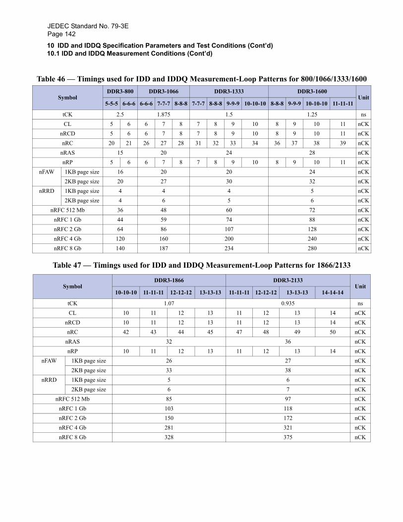
JEDEC Standard No. 79-3EPage 142
Ta 0
nit
sKKKKK
n KK
n KKKKKKK
it
n
10 IDD and IDDQ Specification Parameters and Test Conditions (Cont’d)10.1 IDD and IDDQ Measurement Conditions (Cont’d)
Table 47 — Timings used for IDD and IDDQ Measurement-Loop Patterns for 1866/2133
ble 46 — Timings used for IDD and IDDQ Measurement-Loop Patterns for 800/1066/1333/160
SymbolDDR3-800 DDR3-1066 DDR3-1333 DDR3-1600
U5-5-5 6-6-6 6-6-6 7-7-7 8-8-8 7-7-7 8-8-8 9-9-9 10-10-10 8-8-8 9-9-9 10-10-10 11-11-11
tCK 2.5 1.875 1.5 1.25 nCL 5 6 6 7 8 7 8 9 10 8 9 10 11 nC
nRCD 5 6 6 7 8 7 8 9 10 8 9 10 11 nCnRC 20 21 26 27 28 31 32 33 34 36 37 38 39 nC
nRAS 15 20 24 28 nCnRP 5 6 6 7 8 7 8 9 10 8 9 10 11 nC
FAW 1KB page size 16 20 20 24 nC2KB page size 20 27 30 32 nC
RRD 1KB page size 4 4 4 5 nC2KB page size 4 6 5 6 nC
nRFC 512 Mb 36 48 60 72 nCnRFC 1 Gb 44 59 74 88 nCnRFC 2 Gb 64 86 107 128 nCnRFC 4 Gb 120 160 200 240 nCnRFC 8 Gb 140 187 234 280 nC
SymbolDDR3-1866 DDR3-2133
Un10-10-10 11-11-11 12-12-12 13-13-13 11-11-11 12-12-12 13-13-13 14-14-14
tCK 1.07 0.935 nsCL 10 11 12 13 11 12 13 14 nCK
nRCD 10 11 12 13 11 12 13 14 nCKnRC 42 43 44 45 47 48 49 50 nCK
nRAS 32 36 nCKnRP 10 11 12 13 11 12 13 14 nCK
FAW 1KB page size 26 27 nCK2KB page size 33 38 nCK
nRRD 1KB page size 5 6 nCK2KB page size 6 7 nCK
nRFC 512 Mb 85 97 nCKnRFC 1 Gb 103 118 nCKnRFC 2 Gb 150 172 nCKnRFC 4 Gb 281 321 nCKnRFC 8 Gb 328 375 nCK
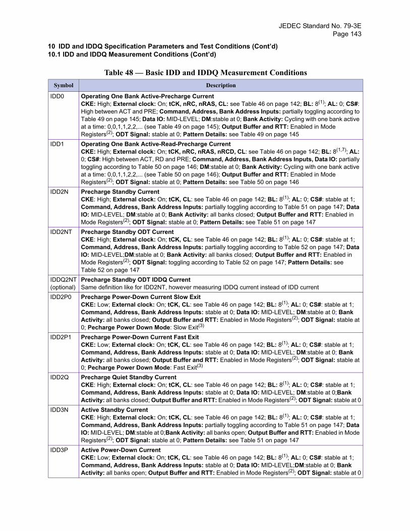
JEDEC Standard No. 79-3EPage 143
10 IDD and IDDQ Specification Parameters and Test Conditions (Cont’d)10.1 IDD and IDDQ Measurement Conditions (Cont’d)
Table 48 — Basic IDD and IDDQ Measurement ConditionsSymbol Description
IDD0 Operating One Bank Active-Precharge CurrentCKE: High; External clock: On; tCK, nRC, nRAS, CL: see Table 46 on page 142; BL: 8(1); AL: 0; CS#: High between ACT and PRE; Command, Address, Bank Address Inputs: partially toggling according to Table 49 on page 145; Data IO: MID-LEVEL; DM:stable at 0; Bank Activity: Cycling with one bank active at a time: 0,0,1,1,2,2,... (see Table 49 on page 145); Output Buffer and RTT: Enabled in Mode Registers(2); ODT Signal: stable at 0; Pattern Details: see Table 49 on page 145
IDD1 Operating One Bank Active-Read-Precharge CurrentCKE: High; External clock: On; tCK, nRC, nRAS, nRCD, CL: see Table 46 on page 142; BL: 8(1,7); AL: 0; CS#: High between ACT, RD and PRE; Command, Address, Bank Address Inputs, Data IO: partially toggling according to Table 50 on page 146; DM:stable at 0; Bank Activity: Cycling with one bank active at a time: 0,0,1,1,2,2,... (see Table 50 on page 146); Output Buffer and RTT: Enabled in Mode Registers(2); ODT Signal: stable at 0; Pattern Details: see Table 50 on page 146
IDD2N Precharge Standby CurrentCKE: High; External clock: On; tCK, CL: see Table 46 on page 142; BL: 8(1); AL: 0; CS#: stable at 1; Command, Address, Bank Address Inputs: partially toggling according to Table 51 on page 147; Data IO: MID-LEVEL; DM:stable at 0; Bank Activity: all banks closed; Output Buffer and RTT: Enabled in Mode Registers(2); ODT Signal: stable at 0; Pattern Details: see Table 51 on page 147
IDD2NT Precharge Standby ODT CurrentCKE: High; External clock: On; tCK, CL: see Table 46 on page 142; BL: 8(1); AL: 0; CS#: stable at 1; Command, Address, Bank Address Inputs: partially toggling according to Table 52 on page 147; Data IO: MID-LEVEL;DM:stable at 0; Bank Activity: all banks closed; Output Buffer and RTT: Enabled in Mode Registers(2); ODT Signal: toggling according to Table 52 on page 147; Pattern Details: see Table 52 on page 147
IDDQ2NT(optional)
Precharge Standby ODT IDDQ CurrentSame definition like for IDD2NT, however measuring IDDQ current instead of IDD current
IDD2P0 Precharge Power-Down Current Slow ExitCKE: Low; External clock: On; tCK, CL: see Table 46 on page 142; BL: 8(1); AL: 0; CS#: stable at 1; Command, Address, Bank Address Inputs: stable at 0; Data IO: MID-LEVEL; DM:stable at 0; Bank Activity: all banks closed; Output Buffer and RTT: Enabled in Mode Registers(2); ODT Signal: stable at 0; Pecharge Power Down Mode: Slow Exit(3)
IDD2P1 Precharge Power-Down Current Fast ExitCKE: Low; External clock: On; tCK, CL: see Table 46 on page 142; BL: 8(1); AL: 0; CS#: stable at 1; Command, Address, Bank Address Inputs: stable at 0; Data IO: MID-LEVEL; DM:stable at 0; Bank Activity: all banks closed; Output Buffer and RTT: Enabled in Mode Registers(2); ODT Signal: stable at 0; Pecharge Power Down Mode: Fast Exit(3)
IDD2Q Precharge Quiet Standby CurrentCKE: High; External clock: On; tCK, CL: see Table 46 on page 142; BL: 8(1); AL: 0; CS#: stable at 1; Command, Address, Bank Address Inputs: stable at 0; Data IO: MID-LEVEL; DM:stable at 0;Bank Activity: all banks closed; Output Buffer and RTT: Enabled in Mode Registers(2); ODT Signal: stable at 0
IDD3N Active Standby CurrentCKE: High; External clock: On; tCK, CL: see Table 46 on page 142; BL: 8(1); AL: 0; CS#: stable at 1; Command, Address, Bank Address Inputs: partially toggling according to Table 51 on page 147; Data IO: MID-LEVEL; DM:stable at 0;Bank Activity: all banks open; Output Buffer and RTT: Enabled in Mode Registers(2); ODT Signal: stable at 0; Pattern Details: see Table 51 on page 147
IDD3P Active Power-Down CurrentCKE: Low; External clock: On; tCK, CL: see Table 46 on page 142; BL: 8(1); AL: 0; CS#: stable at 1; Command, Address, Bank Address Inputs: stable at 0; Data IO: MID-LEVEL;DM:stable at 0; Bank Activity: all banks open; Output Buffer and RTT: Enabled in Mode Registers(2); ODT Signal: stable at 0

JEDEC Standard No. 79-3EPage 144
10 IDD and IDDQ Specification Parameters and Test Conditions (Cont’d)10.1 IDD and IDDQ Measurement Conditions (Cont’d)
IDD4R Operating Burst Read CurrentCKE: High; External clock: On; tCK, CL: see Table 46 on page 142; BL: 8(1,7); AL: 0; CS#: High between RD; Command, Address, Bank Address Inputs: partially toggling according to Table 53 on page 148; Data IO: seamless read data burst with different data between one burst and the next one according to Table 53 on page 148; DM:stable at 0; Bank Activity: all banks open, RD commands cycling through banks: 0,0,1,1,2,2,... (see Table 53 on page 148); Output Buffer and RTT: Enabled in Mode Registers(2); ODT Signal: stable at 0; Pattern Details: see Table 53 on page 148
IDDQ4R(optional)
Operating Burst Read IDDQ CurrentSame definition like for IDD4R, however measuring IDDQ current instead of IDD current
IDD4W Operating Burst Write CurrentCKE: High; External clock: On; tCK, CL: see Table 46 on page 142; BL: 8(1); AL: 0; CS#: High between WR; Command, Address, Bank Address Inputs: partially toggling according to Table 54 on page 148; Data IO: seamless write data burst with different data between one burst and the next one according to Table 54 on page 148; DM: stable at 0; Bank Activity: all banks open, WR commands cycling through banks: 0,0,1,1,2,2,... (see Table 54 on page 148); Output Buffer and RTT: Enabled in Mode Registers(2); ODT Signal: stable at HIGH; Pattern Details: see Table 54 on page 148
IDD5B Burst Refresh CurrentCKE: High; External clock: On; tCK, CL, nRFC: see Table 46 on page 142; BL: 8(1); AL: 0; CS#: High between REF; Command, Address, Bank Address Inputs: partially toggling according to Table 55 on page 149; Data IO: MID-LEVEL;DM:stable at 0; Bank Activity: REF command every nRFC (see Table 55 on page 149); Output Buffer and RTT: Enabled in Mode Registers(2); ODT Signal: stable at 0; Pattern Details: see Table 55 on page 149
IDD6 Self Refresh Current: Normal Temperature RangeTCASE: 0 - 85°C; Auto Self-Refresh (ASR): Disabled(4); Self-Refresh Temperature Range (SRT): Normal(5); CKE: Low; External clock: Off; CK and CK#: LOW; CL: see Table 46 on page 142; BL: 8(1); AL: 0; CS#, Command, Address, Bank Address, Data IO: MID-LEVEL;DM:stable at 0; Bank Activity: Self-Refresh operation; Output Buffer and RTT: Enabled in Mode Registers(2); ODT Signal: MID-LEVEL
IDD6ET Self-Refresh Current: Extended Temperature Range (optional)(6)
TCASE: 0 - 95°C; Auto Self-Refresh (ASR): Disabled(4); Self-Refresh Temperature Range (SRT): Extended(5); CKE: Low; External clock: Off; CK and CK#: LOW; CL: see Table 46 on page 142; BL: 8(1); AL: 0; CS#, Command, Address, Bank Address, Data IO: MID-LEVEL;DM:stable at 0; Bank Activity: Extended Temperature Self-Refresh operation; Output Buffer and RTT: Enabled in Mode Registers(2); ODT Signal: MID-LEVEL
IDD6TC Auto Self-Refresh Current (optional)(6)
TCASE: 0 - 95°C; Auto Self-Refresh (ASR): Enabled(4); Self-Refresh Temperature Range (SRT): Normal(5); CKE: Low; External clock: Off; CK and CK#: LOW; CL: see Table 46 on page 142; BL: 8(1); AL: 0; CS#, Command, Address, Bank Address, Data IO: MID-LEVEL; DM:stable at 0; Bank Activity: Auto Self-Refresh operation; Output Buffer and RTT: Enabled in Mode Registers(2); ODT Signal: MID-LEVEL
IDD7 Operating Bank Interleave Read CurrentCKE: High; External clock: On; tCK, nRC, nRAS, nRCD, nRRD, nFAW, CL: see Table 46 on page 142; BL: 8(1,7); AL: CL-1; CS#: High between ACT and RDA; Command, Address, Bank Address Inputs: partially toggling according to Table 56 on page 150; Data IO: read data bursts with different data between one burst and the next one according to Table 56 on page 150; DM:stable at 0; Bank Activity: two times interleaved cycling through banks (0, 1, ...7) with different addressing, see Table 56 on page 150; Output Buffer and RTT: Enabled in Mode Registers(2); ODT Signal: stable at 0; Pattern Details: see Table 56 on page 150
Table 48 — Basic IDD and IDDQ Measurement ConditionsSymbol Description
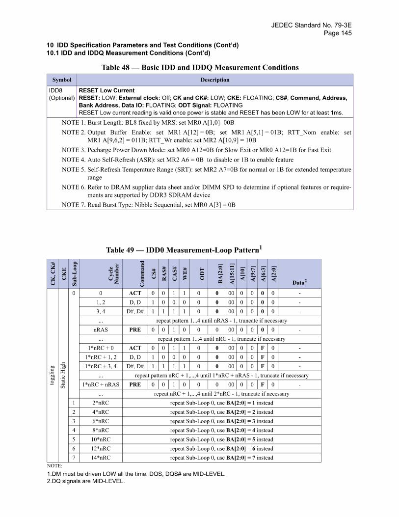
JEDEC Standard No. 79-3EPage 145
10 IDD Specification Parameters and Test Conditions (Cont’d)10.1 IDD and IDDQ Measurement Conditions (Cont’d)
IDD8(Optional)
RESET Low CurrentRESET: LOW; External clock: Off; CK and CK#: LOW; CKE: FLOATING; CS#, Command, Address, Bank Address, Data IO: FLOATING; ODT Signal: FLOATINGRESET Low current reading is valid once power is stable and RESET has been LOW for at least 1ms.
NOTE 1. Burst Length: BL8 fixed by MRS: set MR0 A[1,0]=00BNOTE 2. Output Buffer Enable: set MR1 A[12] = 0B; set MR1 A[5,1] = 01B; RTT_Nom enable: set
MR1 A[9,6,2] = 011B; RTT_Wr enable: set MR2 A[10,9] = 10BNOTE 3. Pecharge Power Down Mode: set MR0 A12=0B for Slow Exit or MR0 A12=1B for Fast ExitNOTE 4. Auto Self-Refresh (ASR): set MR2 A6 = 0B to disable or 1B to enable featureNOTE 5. Self-Refresh Temperature Range (SRT): set MR2 A7=0B for normal or 1B for extended temperature
rangeNOTE 6. Refer to DRAM supplier data sheet and/or DIMM SPD to determine if optional features or require-
ments are supported by DDR3 SDRAM deviceNOTE 7. Read Burst Type: Nibble Sequential, set MR0 A[3] = 0B
Table 49 — IDD0 Measurement-Loop Pattern1
NOTE:1.DM must be driven LOW all the time. DQS, DQS# are MID-LEVEL.
CK
, CK
#
CK
E
Sub-
Loo
p
Cyc
leN
umbe
r
Com
man
d
CS#
RA
S#
CA
S#
WE
#
OD
T
BA
[2:0
]
A[1
5:11
]
A[1
0]
A[9
:7]
A[6
:3]
A[2
:0]
Data2
2.DQ signals are MID-LEVEL.
togg
ling
Stat
ic H
igh
0 0 ACT 0 0 1 1 0 0 00 0 0 0 0 -1, 2 D, D 1 0 0 0 0 0 00 0 0 0 0 -3, 4 D#, D# 1 1 1 1 0 0 00 0 0 0 0 -... repeat pattern 1...4 until nRAS - 1, truncate if necessary
nRAS PRE 0 0 1 0 0 0 00 0 0 0 0 -... repeat pattern 1...4 until nRC - 1, truncate if necessary
1*nRC + 0 ACT 0 0 1 1 0 0 00 0 0 F 0 -1*nRC + 1, 2 D, D 1 0 0 0 0 0 00 0 0 F 0 -1*nRC + 3, 4 D#, D# 1 1 1 1 0 0 00 0 0 F 0 -
... repeat pattern nRC + 1,...,4 until 1*nRC + nRAS - 1, truncate if necessary1*nRC + nRAS PRE 0 0 1 0 0 0 00 0 0 F 0 -
... repeat nRC + 1,...,4 until 2*nRC - 1, truncate if necessary1 2*nRC repeat Sub-Loop 0, use BA[2:0] = 1 instead2 4*nRC repeat Sub-Loop 0, use BA[2:0] = 2 instead3 6*nRC repeat Sub-Loop 0, use BA[2:0] = 3 instead4 8*nRC repeat Sub-Loop 0, use BA[2:0] = 4 instead5 10*nRC repeat Sub-Loop 0, use BA[2:0] = 5 instead6 12*nRC repeat Sub-Loop 0, use BA[2:0] = 6 instead7 14*nRC repeat Sub-Loop 0, use BA[2:0] = 7 instead
Table 48 — Basic IDD and IDDQ Measurement ConditionsSymbol Description
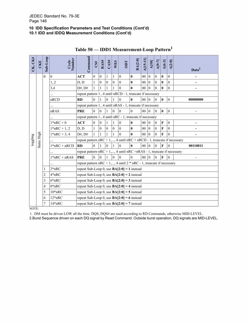
JEDEC Standard No. 79-3EPage 146
10 IDD Specification Parameters and Test Conditions (Cont’d)10.1 IDD and IDDQ Measurement Conditions (Cont’d)
Table 50 — IDD1 Measurement-Loop Pattern1
NOTE:1. DM must be driven LOW all the time. DQS, DQS# are used according to RD Commands, otherwise MID-LEVEL.
CK
, CK
#
CK
E
Sub-
Loo
p
Cyc
leN
umbe
r
Com
man
d
CS#
RA
S#
CA
S#
WE
#
OD
T
BA
[2:0
]
A[1
5:11
]
A[1
0]
A[9
:7]
A[6
:3]
A[2
:0]
Data2
2.Burst Sequence driven on each DQ signal by Read Command. Outside burst operation, DQ signals are MID-LEVEL.
togg
ling
Stat
ic H
igh
0 0 ACT 0 0 1 1 0 0 00 0 0 0 0 -1, 2 D, D 1 0 0 0 0 0 00 0 0 0 0 -3,4 D#, D# 1 1 1 1 0 0 00 0 0 0 0 -... repeat pattern 1...4 until nRCD - 1, truncate if necessary nRCD RD 0 1 0 1 0 0 00 0 0 0 0 00000000... repeat pattern 1...4 until nRAS - 1, truncate if necessary nRAS PRE 0 0 1 0 0 0 00 0 0 0 0 -... repeat pattern 1...4 until nRC - 1, truncate if necessary1*nRC + 0 ACT 0 0 1 1 0 0 00 0 0 F 0 -1*nRC + 1, 2 D, D 1 0 0 0 0 0 00 0 0 F 0 -1*nRC + 3, 4 D#, D# 1 1 1 1 0 0 00 0 0 F 0 -... repeat pattern nRC + 1,..., 4 until nRC + nRCD - 1, truncate if necessary1*nRC + nRCD RD 0 1 0 1 0 0 00 0 0 F 0 00110011... repeat pattern nRC + 1,..., 4 until nRC +nRAS - 1, truncate if necessary1*nRC + nRAS PRE 0 0 1 0 0 0 00 0 0 F 0 -... repeat pattern nRC + 1,..., 4 until 2 * nRC - 1, truncate if necessary
1 2*nRC repeat Sub-Loop 0, use BA[2:0] = 1 instead2 4*nRC repeat Sub-Loop 0, use BA[2:0] = 2 instead3 6*nRC repeat Sub-Loop 0, use BA[2:0] = 3 instead4 8*nRC repeat Sub-Loop 0, use BA[2:0] = 4 instead5 10*nRC repeat Sub-Loop 0, use BA[2:0] = 5 instead6 12*nRC repeat Sub-Loop 0, use BA[2:0] = 6 instead7 14*nRC repeat Sub-Loop 0, use BA[2:0] = 7 instead
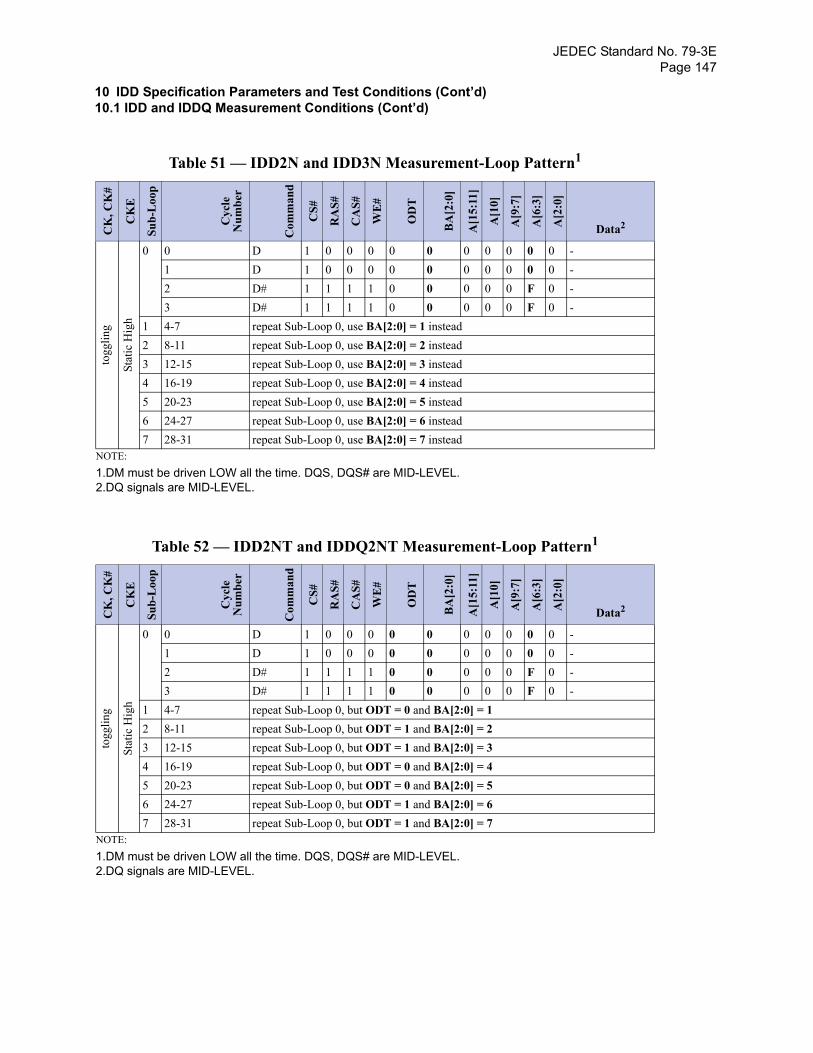
JEDEC Standard No. 79-3EPage 147
10 IDD Specification Parameters and Test Conditions (Cont’d)10.1 IDD and IDDQ Measurement Conditions (Cont’d)
Table 51 — IDD2N and IDD3N Measurement-Loop Pattern1
NOTE:1.DM must be driven LOW all the time. DQS, DQS# are MID-LEVEL.
CK
, CK
#
CK
E
Sub-
Loo
p
Cyc
leN
umbe
r
Com
man
d
CS#
RA
S#
CA
S#
WE
#
OD
T
BA
[2:0
]
A[1
5:11
]
A[1
0]
A[9
:7]
A[6
:3]
A[2
:0]
Data2
2.DQ signals are MID-LEVEL.
togg
ling
Stat
ic H
igh
0 0 D 1 0 0 0 0 0 0 0 0 0 0 -1 D 1 0 0 0 0 0 0 0 0 0 0 -2 D# 1 1 1 1 0 0 0 0 0 F 0 -3 D# 1 1 1 1 0 0 0 0 0 F 0 -
1 4-7 repeat Sub-Loop 0, use BA[2:0] = 1 instead2 8-11 repeat Sub-Loop 0, use BA[2:0] = 2 instead3 12-15 repeat Sub-Loop 0, use BA[2:0] = 3 instead4 16-19 repeat Sub-Loop 0, use BA[2:0] = 4 instead5 20-23 repeat Sub-Loop 0, use BA[2:0] = 5 instead6 24-27 repeat Sub-Loop 0, use BA[2:0] = 6 instead7 28-31 repeat Sub-Loop 0, use BA[2:0] = 7 instead
Table 52 — IDD2NT and IDDQ2NT Measurement-Loop Pattern1
NOTE:1.DM must be driven LOW all the time. DQS, DQS# are MID-LEVEL.
CK
, CK
#
CK
E
Sub-
Loo
p
Cyc
leN
umbe
r
Com
man
d
CS#
RA
S#
CA
S#
WE
#
OD
T
BA
[2:0
]
A[1
5:11
]
A[1
0]
A[9
:7]
A[6
:3]
A[2
:0]
Data2
2.DQ signals are MID-LEVEL.
togg
ling
Stat
ic H
igh
0 0 D 1 0 0 0 0 0 0 0 0 0 0 -1 D 1 0 0 0 0 0 0 0 0 0 0 -2 D# 1 1 1 1 0 0 0 0 0 F 0 -3 D# 1 1 1 1 0 0 0 0 0 F 0 -
1 4-7 repeat Sub-Loop 0, but ODT = 0 and BA[2:0] = 12 8-11 repeat Sub-Loop 0, but ODT = 1 and BA[2:0] = 23 12-15 repeat Sub-Loop 0, but ODT = 1 and BA[2:0] = 34 16-19 repeat Sub-Loop 0, but ODT = 0 and BA[2:0] = 45 20-23 repeat Sub-Loop 0, but ODT = 0 and BA[2:0] = 56 24-27 repeat Sub-Loop 0, but ODT = 1 and BA[2:0] = 67 28-31 repeat Sub-Loop 0, but ODT = 1 and BA[2:0] = 7

JEDEC Standard No. 79-3EPage 148
10 IDD Specification Parameters and Test Conditions (Cont’d)10.1 IDD and IDDQ Measurement Conditions (Cont’d)
Table 53 — IDD4R and IDDQ4R Measurement-Loop Pattern1
NOTE:1.DM must be driven LOW all the time. DQS, DQS# are used according to RD Commands, otherwise MID-LEVEL.
CK
, CK
#
CK
E
Sub-
Loo
p
Cyc
leN
umbe
r
Com
man
d
CS#
RA
S#
CA
S#
WE
#
OD
T
BA
[2:0
]
A[1
5:11
]
A[1
0]
A[9
:7]
A[6
:3]
A[2
:0]
Data2
2.Burst Sequence driven on each DQ signal by Read Command. Outside burst operation, DQ signals are MID-LEVEL.
togg
ling
Stat
ic H
igh
0 0 RD 0 1 0 1 0 0 00 0 0 0 0 000000001 D 1 0 0 0 0 0 00 0 0 0 0 -2, 3 D#,D# 1 1 1 1 0 0 00 0 0 0 0 -4 RD 0 1 0 1 0 0 00 0 0 F 0 001100115 D 1 0 0 0 0 0 00 0 0 F 0 -6, 7 D#,D# 1 1 1 1 0 0 00 0 0 F 0 -
1 8-15 repeat Sub-Loop 0, but BA[2:0] = 12 16-23 repeat Sub-Loop 0, but BA[2:0] = 23 24-31 repeat Sub-Loop 0, but BA[2:0] = 34 32-39 repeat Sub-Loop 0, but BA[2:0] = 45 40-47 repeat Sub-Loop 0, but BA[2:0] = 56 48-55 repeat Sub-Loop 0, but BA[2:0] = 67 56-63 repeat Sub-Loop 0, but BA[2:0] = 7
Table 54 — IDD4W Measurement-Loop Pattern1
NOTE:1.DM must be driven LOW all the time. DQS, DQS# are used according to WR Commands, otherwise MID-LEVEL.
CK
, CK
#
CK
E
Sub-
Loo
p
Cyc
leN
umbe
r
Com
man
d
CS#
RA
S#
CA
S#
WE
#
OD
T
BA
[2:0
]
A[1
5:11
]
A[1
0]
A[9
:7]
A[6
:3]
A[2
:0]
Data2
2.Burst Sequence driven on each DQ signal by Write Command. Outside burst operation, DQ signals are MID-LEVEL.
togg
ling
Stat
ic H
igh
0 0 WR 0 1 0 0 1 0 00 0 0 0 0 000000001 D 1 0 0 0 1 0 00 0 0 0 0 -2, 3 D#,D# 1 1 1 1 1 0 00 0 0 0 0 -4 WR 0 1 0 0 1 0 00 0 0 F 0 001100115 D 1 0 0 0 1 0 00 0 0 F 0 -6, 7 D#,D# 1 1 1 1 1 0 00 0 0 F 0 -
1 8-15 repeat Sub-Loop 0, but BA[2:0] = 12 16-23 repeat Sub-Loop 0, but BA[2:0] = 23 24-31 repeat Sub-Loop 0, but BA[2:0] = 34 32-39 repeat Sub-Loop 0, but BA[2:0] = 45 40-47 repeat Sub-Loop 0, but BA[2:0] = 56 48-55 repeat Sub-Loop 0, but BA[2:0] = 67 56-63 repeat Sub-Loop 0, but BA[2:0] = 7
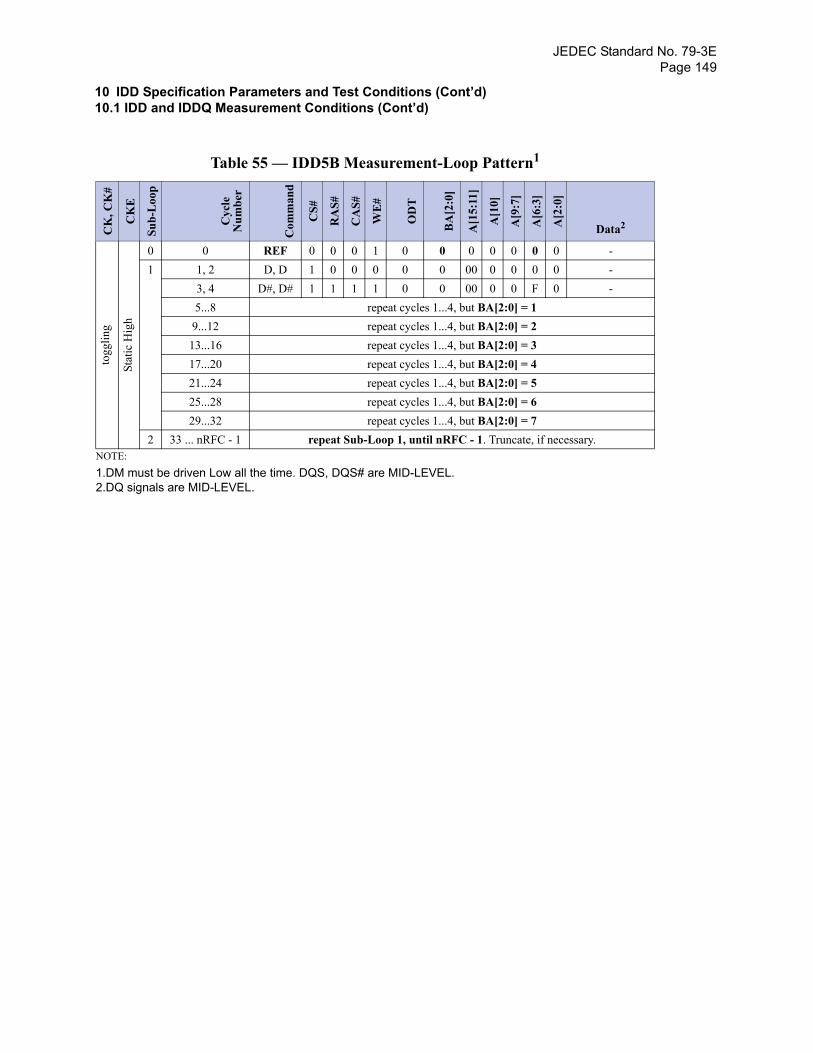
JEDEC Standard No. 79-3EPage 149
10 IDD Specification Parameters and Test Conditions (Cont’d)10.1 IDD and IDDQ Measurement Conditions (Cont’d)
Table 55 — IDD5B Measurement-Loop Pattern1
NOTE:1.DM must be driven Low all the time. DQS, DQS# are MID-LEVEL.
CK
, CK
#
CK
E
Sub-
Loo
p
Cyc
leN
umbe
r
Com
man
d
CS#
RA
S#
CA
S#
WE
#
OD
T
BA
[2:0
]
A[1
5:11
]
A[1
0]
A[9
:7]
A[6
:3]
A[2
:0]
Data2
2.DQ signals are MID-LEVEL.
togg
ling
Stat
ic H
igh
0 0 REF 0 0 0 1 0 0 0 0 0 0 0 -1 1, 2 D, D 1 0 0 0 0 0 00 0 0 0 0 -
3, 4 D#, D# 1 1 1 1 0 0 00 0 0 F 0 -5...8 repeat cycles 1...4, but BA[2:0] = 1
9...12 repeat cycles 1...4, but BA[2:0] = 213...16 repeat cycles 1...4, but BA[2:0] = 317...20 repeat cycles 1...4, but BA[2:0] = 421...24 repeat cycles 1...4, but BA[2:0] = 525...28 repeat cycles 1...4, but BA[2:0] = 629...32 repeat cycles 1...4, but BA[2:0] = 7
2 33 ... nRFC - 1 repeat Sub-Loop 1, until nRFC - 1. Truncate, if necessary.

JEDEC Standard No. 79-3EPage 150
10 IDD Specification Parameters and Test Conditions (Cont’d)10.1 IDD and IDDQ Measurement Conditions (Cont’d)
Table 56 — IDD7 Measurement-Loop Pattern1
ATTENTION: Sub-Loops 10-19 have inverse A[6:3] Pattern and Data Pattern than Sub-Loops 0-9
NOTE:1.DM must be driven LOW all the time. DQS, DQS# are used according to RD Commands, otherwise MID-LEVEL
CK
, CK
#
CK
E
Sub-
Loo
p
Cyc
leN
umbe
r
Com
man
d
CS#
RA
S#
CA
S#
WE
#
OD
T
BA
[2:0
]
A[1
5:11
]
A[1
0]
A[9
:7]
A[6
:3]
A[2
:0]
Data2
2.Burst Sequence driven on each DQ signal by Read Command. Outside burst operation, DQ signals are MID-LEVEL.
togg
ling
Stat
ic H
igh
0 0 ACT 0 0 1 1 0 0 00 0 0 0 0 -1 RDA 0 1 0 1 0 0 00 1 0 0 0 000000002 D 1 0 0 0 0 0 00 0 0 0 0 -... repeat above D Command until nRRD - 1
1 nRRD ACT 0 0 1 1 0 1 00 0 0 F 0 -nRRD + 1 RDA 0 1 0 1 0 1 00 1 0 F 0 00110011nRRD + 2 D 1 0 0 0 0 1 00 0 0 F 0 -... repeat above D Command until 2 * nRRD -1
2 2 * nRRD repeat Sub-Loop 0, but BA[2:0] = 23 3 * nRRD repeat Sub-Loop 1, but BA[2:0] = 34 4 * nRRD D 1 0 0 0 0 3 00 0 0 F 0 -
Assert and repeat above D Command until nFAW - 1, if necessary5 nFAW repeat Sub-Loop 0, but BA[2:0] = 46 nFAW+nRRD repeat Sub-Loop 1, but BA[2:0] = 57 nFAW+2*nRRD repeat Sub-Loop 0, but BA[2:0] = 68 nFAW+3*nRRD repeat Sub-Loop 1, but BA[2:0] = 79 nFAW+4*nRRD D 1 0 0 0 0 7 00 0 0 F 0 -
Assert and repeat above D Command until 2 * nFAW - 1, if necessary
10 2*nFAW+0 ACT 0 0 1 1 0 0 00 0 0 F 0 -2*nFAW+1 RDA 0 1 0 1 0 0 00 1 0 F 0 001100112*nFAW+2 D 1 0 0 0 0 0 00 0 0 F 0 -
Repeat above D Command until 2 * nFAW + nRRD - 111 2*nFAW+nRRD ACT 0 0 1 1 0 1 00 0 0 0 0 -
2*nFAW+nRRD+1 RDA 0 1 0 1 0 1 00 1 0 0 0 000000002*nFAW+nRRD+2 D 1 0 0 0 0 1 00 0 0 0 0 -
repeat above D Command until 2 * nFAW + 2 * nRRD -112 2*nFAW+2*nRRD repeat Sub-Loop 10, but BA[2:0] = 213 2*nFAW+3*nRRD repeat Sub-Loop 11, but BA[2:0] = 314 2*nFAW+4 * nRRD D 1 0 0 0 0 3 00 0 0 0 0 -
Assert and repeat above D Command until 3 * nFAW - 1, if necessary15 3*nFAW repeat Sub-Loop 10, but BA[2:0] = 416 3*nFAW+nRRD repeat Sub-Loop 11, but BA[2:0] = 517 3*nFAW+2*nRRD repeat Sub-Loop 10, but BA[2:0] = 618 3*nFAW+3*nRRD repeat Sub-Loop 11, but BA[2:0] = 719 3*nFAW+4*nRRD D 1 0 0 0 0 7 00 0 0 0 0 -
Assert and repeat above D Command until 4 * nFAW - 1, if necessary

JEDEC Standard No. 79-3EPage 151
SpeBin
Sym
IDD
IDD
IDD 6
IDD 6
IDD 6
IDD
IDD
IDD 6
IDD 6
IDD 6
IDD
IDD
IDD
IDD 6
IDD n IDD
IDDIDD
M
10 IDD Specification Parameters and Test Conditions (Cont’d)
10.2 IDD SpecificationsIDD values are for full operating range of voltage and temperature unless otherwise noted.
Table 57 — IDD Specification Example 512M DDR3ed Grade DDR3 - 800
5-5-5DDR3 - 1066
7-7-7DDR3 - 1333
8-8-8DDR3 - 1600
9-9-9
Unit Notesbol Max. Max. Max. Max.
0 mA x4/x8mA x16
1 mA x4/x8mA x16
2P (0) slow exit mA x4/x8/x1
2P (1) fast exit mA x4/x8/x1
2N mA x4/x8/x1
2NT mA x4/x8mA x16
Q2NT (Optional) mA x4/x8mA x16
2Q mA x4/x8/x1
3P (fast exit) mA x4/x8/x1
3N mA x4/x8/x1
4R mA x4mA x8mA x16
Q4R (Optional) mA x4mA x8mA x16
4W mA x4mA x8mA x16
5B mA x4/x8/x1
6 mA Refer toTable 58 o
page 1526ET1 mA
6TC1 mA
7 mA x4/x8mA x16
NOTE 1. Users should refer to the DRAM supplier data sheet and/or the DIMM SPD to determine if DDR3 SDRAdevices support the following options or requirements referred to in this material.
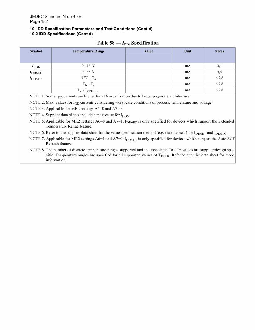
JEDEC Standard No. 79-3EPage 152
ed
elf
e-re
Table 58 — IDD6 SpecificationSymbol Temperature Range Value Unit Notes
IDD6 0 - 85 oC mA 3,4IDD6ET 0 - 95 oC mA 5,6IDD6TC 0 oC ~ Ta mA 6,7,8
Tb ~ Ty mA 6,7,8Tz ~ TOPERmax mA 6,7,8
NOTE 1. Some IDD currents are higher for x16 organization due to larger page-size architecture.NOTE 2. Max. values for IDD currents considering worst case conditions of process, temperature and voltage.NOTE 3. Applicable for MR2 settings A6=0 and A7=0.NOTE 4. Supplier data sheets include a max value for IDD6.NOTE 5. Applicable for MR2 settings A6=0 and A7=1. IDD6ET is only specified for devices which support the Extend
Temperature Range feature.NOTE 6. Refer to the supplier data sheet for the value specification method (e.g. max, typical) for IDD6ET and IDD6TCNOTE 7. Applicable for MR2 settings A6=1 and A7=0. IDD6TC is only specified for devices which support the Auto S
Refresh feature.NOTE 8. The number of discrete temperature ranges supported and the associated Ta - Tz values are supplier/design sp
cific. Temperature ranges are specified for all supported values of TOPER. Refer to supplier data sheet for moinformation.
10 IDD Specification Parameters and Test Conditions (Cont’d)10.2 IDD Specifications (Cont’d)

JEDEC Standard No. 79-3EPage 153
This page left blank.
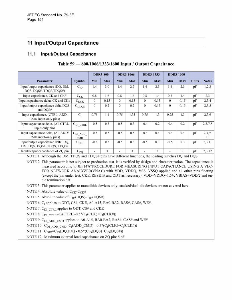
JEDEC Standard No. 79-3EPage 154
es
Inp ,3
IInpu ,4Inp ,5
In ,6
Inp ,8
Inp 9,
InpDM
11
Inp 12
isC-ngn-
11 Input/Output Capacitance
11.1 Input/Output Capacitance
Table 59 — 800/1066/1333/1600 Input / Output Capacitance
DDR3-800 DDR3-1066 DDR3-1333 DDR3-1600
Parameter Symbol Min Max Min Max Min Max Min Max Units Not
ut/output capacitance (DQ, DM, DQS, DQS#, TDQS,TDQS#)
CIO 1.4 3.0 1.4 2.7 1.4 2.5 1.4 2.3 pF 1,2
nput capacitance, CK and CK# CCK 0.8 1.6 0.8 1.6 0.8 1.4 0.8 1.4 pF 2,3t capacitance delta, CK and CK# CDCK 0 0.15 0 0.15 0 0.15 0 0.15 pF 2,3ut/output capacitance delta DQS
and DQS#CDDQS 0 0.2 0 0.2 0 0.15 0 0.15 pF 2,3
put capacitance, (CTRL, ADD, CMD input-only pins)
CI 0.75 1.4 0.75 1.35 0.75 1.3 0.75 1.3 pF 2,3
ut capacitance delta, (All CTRL input-only pins
CDI_CTRL -0.5 0.3 -0.5 0.3 -0.4 0.2 -0.4 0.2 pF 2,3,7
ut capacitance delta, (All ADD/CMD input-only pins)
CDI_ADD_CMD
-0.5 0.5 -0.5 0.5 -0.4 0.4 -0.4 0.4 pF 2,3,10
ut/output capacitance delta, DQ, , DQS, DQS#, TDQS, TDQS#
CDIO -0.5 0.3 -0.5 0.3 -0.5 0.3 -0.5 0.3 pF 2,3,
ut/output capacitance of ZQ pin CZQ - 3 - 3 - 3 - 3 pF 2,3,NOTE 1. Although the DM, TDQS and TDQS# pins have different functions, the loading matches DQ and DQSNOTE 2. This parameter is not subject to production test. It is verified by design and characterization. The capacitance
measured according to JEP147(“PROCEDURE FOR MEASURING INPUT CAPACITANCE USING A VETOR NETWORK ANALYZER(VNA)”) with VDD, VDDQ, VSS, VSSQ applied and all other pins floati(except the pin under test, CKE, RESET# and ODT as necessary). VDD=VDDQ=1.5V, VBIAS=VDD/2 and odie termination off.
NOTE 3. This parameter applies to monolithic devices only; stacked/dual-die devices are not covered hereNOTE 4. Absolute value of CCK-CCK#NOTE 5. Absolute value of CIO(DQS)-CIO(DQS#)NOTE 6. CI applies to ODT, CS#, CKE, A0-A15, BA0-BA2, RAS#, CAS#, WE#. NOTE 7. CDI_CTRL applies to ODT, CS# and CKENOTE 8. CDI_CTRL=CI(CTRL)-0.5*(CI(CLK)+CI(CLK#))NOTE 9. CDI_ADD_CMD applies to A0-A15, BA0-BA2, RAS#, CAS# and WE#NOTE 10. CDI_ADD_CMD=CI(ADD_CMD) - 0.5*(CI(CLK)+CI(CLK#))NOTE 11. CDIO=CIO(DQ,DM) - 0.5*(CIO(DQS)+CIO(DQS#))NOTE 12. Maximum external load capacitance on ZQ pin: 5 pF.
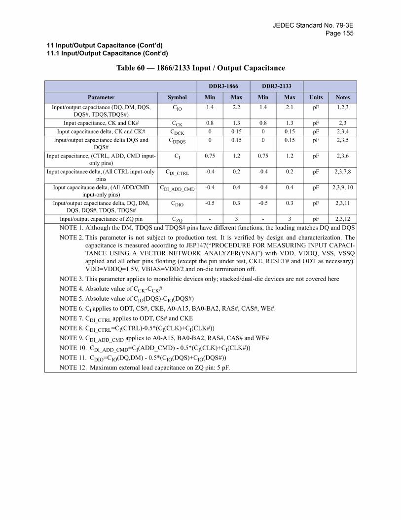
JEDEC Standard No. 79-3EPage 155
Table 60 — 1866/2133 Input / Output Capacitance
DDR3-1866 DDR3-2133
Parameter Symbol Min Max Min Max Units Notes
Input/output capacitance (DQ, DM, DQS, DQS#, TDQS,TDQS#)
CIO 1.4 2.2 1.4 2.1 pF 1,2,3
Input capacitance, CK and CK# CCK 0.8 1.3 0.8 1.3 pF 2,3Input capacitance delta, CK and CK# CDCK 0 0.15 0 0.15 pF 2,3,4
Input/output capacitance delta DQS and DQS#
CDDQS 0 0.15 0 0.15 pF 2,3,5
Input capacitance, (CTRL, ADD, CMD input-only pins)
CI 0.75 1.2 0.75 1.2 pF 2,3,6
Input capacitance delta, (All CTRL input-only pins
CDI_CTRL -0.4 0.2 -0.4 0.2 pF 2,3,7,8
Input capacitance delta, (All ADD/CMD input-only pins)
CDI_ADD_CMD -0.4 0.4 -0.4 0.4 pF 2,3,9, 10
Input/output capacitance delta, DQ, DM, DQS, DQS#, TDQS, TDQS#
CDIO -0.5 0.3 -0.5 0.3 pF 2,3,11
Input/output capacitance of ZQ pin CZQ - 3 - 3 pF 2,3,12NOTE 1. Although the DM, TDQS and TDQS# pins have different functions, the loading matches DQ and DQSNOTE 2. This parameter is not subject to production test. It is verified by design and characterization. The
capacitance is measured according to JEP147(“PROCEDURE FOR MEASURING INPUT CAPACI-TANCE USING A VECTOR NETWORK ANALYZER(VNA)”) with VDD, VDDQ, VSS, VSSQapplied and all other pins floating (except the pin under test, CKE, RESET# and ODT as necessary).VDD=VDDQ=1.5V, VBIAS=VDD/2 and on-die termination off.
NOTE 3. This parameter applies to monolithic devices only; stacked/dual-die devices are not covered hereNOTE 4. Absolute value of CCK-CCK#NOTE 5. Absolute value of CIO(DQS)-CIO(DQS#)NOTE 6. CI applies to ODT, CS#, CKE, A0-A15, BA0-BA2, RAS#, CAS#, WE#. NOTE 7. CDI_CTRL applies to ODT, CS# and CKENOTE 8. CDI_CTRL=CI(CTRL)-0.5*(CI(CLK)+CI(CLK#))NOTE 9. CDI_ADD_CMD applies to A0-A15, BA0-BA2, RAS#, CAS# and WE#NOTE 10. CDI_ADD_CMD=CI(ADD_CMD) - 0.5*(CI(CLK)+CI(CLK#))NOTE 11. CDIO=CIO(DQ,DM) - 0.5*(CIO(DQS)+CIO(DQS#))NOTE 12. Maximum external load capacitance on ZQ pin: 5 pF.
11 Input/Output Capacitance (Cont’d)11.1 Input/Output Capacitance (Cont’d)

JEDEC Standard No. 79-3EPage 156
This page left blank.
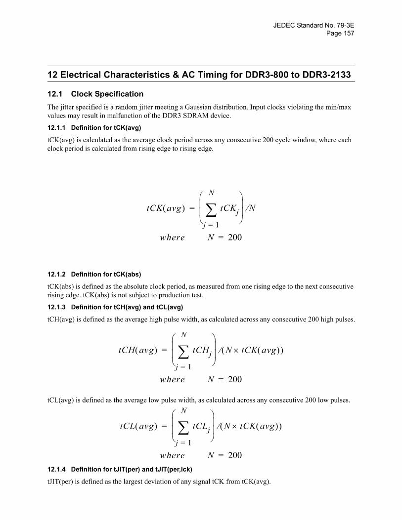
JEDEC Standard No. 79-3EPage 157
12 Electrical Characteristics & AC Timing for DDR3-800 to DDR3-2133
12.1 Clock SpecificationThe jitter specified is a random jitter meeting a Gaussian distribution. Input clocks violating the min/max values may result in malfunction of the DDR3 SDRAM device.
12.1.1 Definition for tCK(avg)
tCK(avg) is calculated as the average clock period across any consecutive 200 cycle window, where each clock period is calculated from rising edge to rising edge.
12.1.2 Definition for tCK(abs)
tCK(abs) is defined as the absolute clock period, as measured from one rising edge to the next consecutive rising edge. tCK(abs) is not subject to production test.
12.1.3 Definition for tCH(avg) and tCL(avg)
tCH(avg) is defined as the average high pulse width, as calculated across any consecutive 200 high pulses.
tCL(avg) is defined as the average low pulse width, as calculated across any consecutive 200 low pulses.
12.1.4 Definition for tJIT(per) and tJIT(per,lck)
tJIT(per) is defined as the largest deviation of any signal tCK from tCK(avg).
tCK avg( ) tCKjj 1=
N
∑⎝ ⎠⎜ ⎟⎜ ⎟⎛ ⎞
N⁄=
where N 200=
tCH avg( ) tCHjj 1=
N
∑⎝ ⎠⎜ ⎟⎜ ⎟⎛ ⎞
N tCK avg( )×( )⁄=
where N 200=
tCL avg( ) tCLjj 1=
N
∑⎝ ⎠⎜ ⎟⎜ ⎟⎛ ⎞
N tCK avg( )×( )⁄=
where N 200=
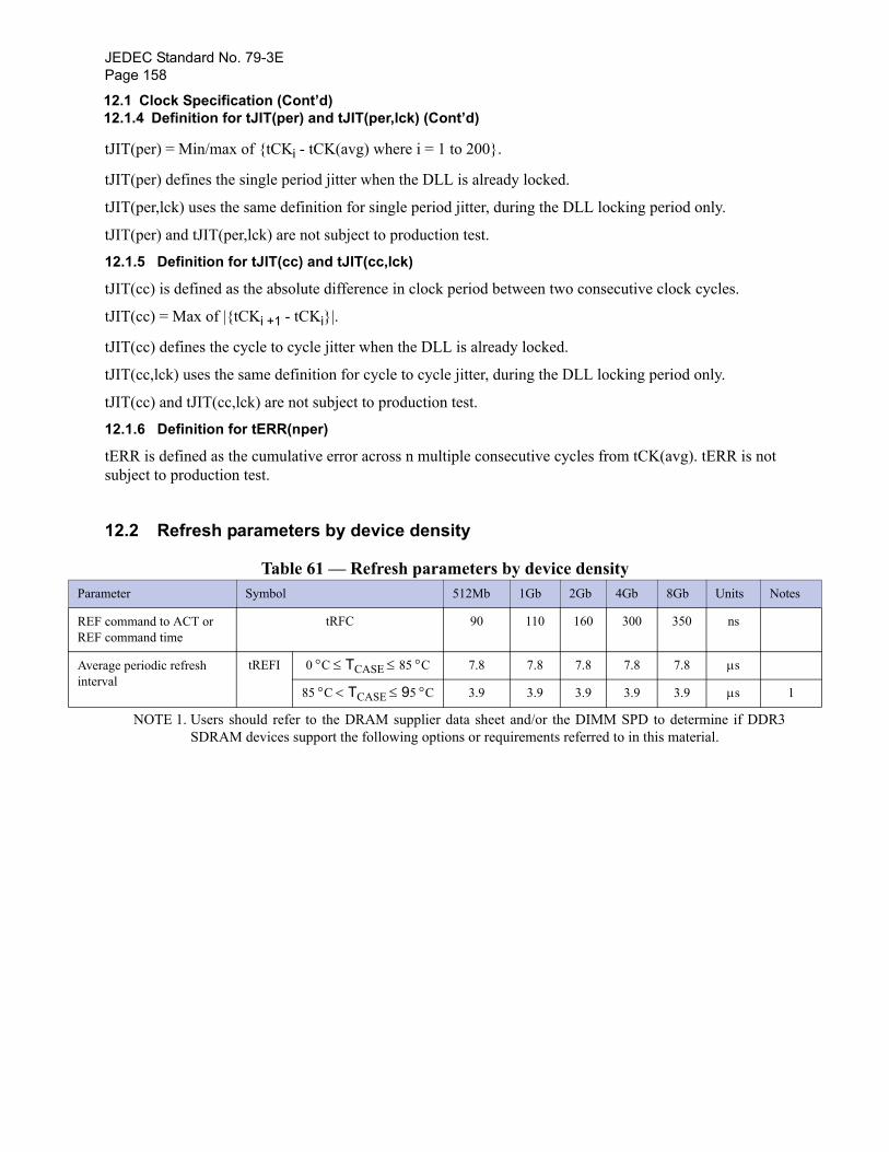
JEDEC Standard No. 79-3EPage 158
Par
RERE
Avinte
12.1 Clock Specification (Cont’d)12.1.4 Definition for tJIT(per) and tJIT(per,lck) (Cont’d)
tJIT(per) = Min/max of {tCKi - tCK(avg) where i = 1 to 200}.
tJIT(per) defines the single period jitter when the DLL is already locked.
tJIT(per,lck) uses the same definition for single period jitter, during the DLL locking period only.
tJIT(per) and tJIT(per,lck) are not subject to production test.
12.1.5 Definition for tJIT(cc) and tJIT(cc,lck)
tJIT(cc) is defined as the absolute difference in clock period between two consecutive clock cycles.
tJIT(cc) = Max of |{tCKi +1 - tCKi}|.
tJIT(cc) defines the cycle to cycle jitter when the DLL is already locked.
tJIT(cc,lck) uses the same definition for cycle to cycle jitter, during the DLL locking period only.
tJIT(cc) and tJIT(cc,lck) are not subject to production test.
12.1.6 Definition for tERR(nper)
tERR is defined as the cumulative error across n multiple consecutive cycles from tCK(avg). tERR is not subject to production test.
12.2 Refresh parameters by device density
Table 61 — Refresh parameters by device density
NOTE 1. Users should refer to the DRAM supplier data sheet and/or the DIMM SPD to determine if DDR3SDRAM devices support the following options or requirements referred to in this material.
ameter Symbol 512Mb 1Gb 2Gb 4Gb 8Gb Units Notes
F command to ACT or F command time
tRFC 90 110 160 300 350 ns
erage periodic refresh rval
tREFI 0 °C ≤ TCASE ≤ 85 °C 7.8 7.8 7.8 7.8 7.8 μs
85 °C < TCASE ≤ 95 °C 3.9 3.9 3.9 3.9 3.9 μs 1
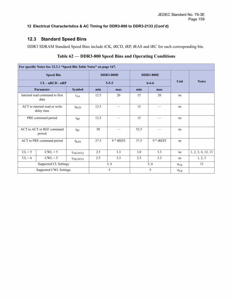
JEDEC Standard No. 79-3EPage 159
For
In
A
AC
A
C 13
C
12 Electrical Characteristics & AC Timing for DDR3-800 to DDR3-2133 (Cont’d)
12.3 Standard Speed BinsDDR3 SDRAM Standard Speed Bins include tCK, tRCD, tRP, tRAS and tRC for each corresponding bin.
Table 62 — DDR3-800 Speed Bins and Operating Conditions
specific Notes See 12.3.1 “Speed Bin Table Notes” on page 167.
Speed Bin DDR3-800D DDR3-800E
Unit NotesCL - nRCD - nRP 5-5-5 6-6-6
Parameter Symbol min max min max
ternal read command to first data
tAA 12.5 20 15 20 ns
CT to internal read or write delay time
tRCD 12.5 — 15 — ns
PRE command period tRP 12.5 — 15 — ns
T to ACT or REF command period
tRC 50 — 52.5 — ns
CT to PRE command period tRAS 37.5 9 * tREFI 37.5 9 * tREFI ns
L = 5 CWL = 5 tCK(AVG) 2.5 3.3 3.0 3.3 ns 1, 2, 3, 4, 12,
L = 6 CWL = 5 tCK(AVG) 2.5 3.3 2.5 3.3 ns 1, 2, 3
Supported CL Settings 5, 6 5, 6 nCK 13
Supported CWL Settings 5 5 nCK

JEDEC Standard No. 79-3EPage 160
For
In
AC
A
CL ,13
CL
CL
CL
12 Electrical Characteristics & AC Timing for DDR3-800 to DDR3-2133 (Cont’d)12.3 Standard Speed Bins (Cont’d)
Table 63 — DDR3-1066 Speed Bins and Operating Conditions
specific Notes See 12.3.1 “Speed Bin Table Notes” on page 167.
Speed Bin DDR3-1066E DDR3-1066F DDR3-1066G
Unit NoteCL - nRCD - nRP 6-6-6 7-7-7 8-8-8
Parameter Symbol min max min max min max
ternal read command to first data
tAA 11.25 20 13.125 20 15 20 ns
T to internal read or write delay time
tRCD 11.25 — 13.125 — 15 — ns
PRE command period tRP 11.25 — 13.125 — 15 — ns
ACT to ACT or REF command period
tRC 48.75 — 50.625 — 52.5 — ns
CT to PRE command period
tRAS 37.5 9 * tREFI 37.5 9 * tREFI 37.5 9 * tREFI ns
= 5 CWL = 5 tCK(AVG) 2.5 3.3 3.0 3.3 3.0 3.3 ns 1,2,3,4,6,12
CWL = 6 tCK(AVG) Reserved Reserved Reserved ns 4,
= 6 CWL = 5 tCK(AVG) 2.5 3.3 2.5 3.3 2.5 3.3 ns 1,2,3,6,
CWL = 6 tCK(AVG) 1.875< 2.5
Reserved Reserved ns 1,2,3,4,
= 7 CWL = 5 tCK(AVG) Reserved Reserved Reserved ns 4,
CWL = 6 tCK(AVG) 1.875 < 2.5 1.875 < 2.5 Reserved ns 1,2,3,4,
= 8 CWL = 5 tCK(AVG) Reserved Reserved Reserved ns 4,
CWL = 6 tCK(AVG) 1.875 < 2.5 1.875 < 2.5 1.875 < 2.5 ns 1,2,3,
Supported CL Settings 5, 6, 7, 8 5, 6, 7, 8 5, 6, 8 nCK 13
Supported CWL Settings 5, 6 5, 6 5, 6 nCK

JEDEC Standard No. 79-3EPage 161
For sp
te
Interna
ACT w
PRE
ACTco
ACT
CL = ,7,12,
CL = 3,7
,4,7
CL =
,4,7
3,4
CL =
3,7
3,4
CL =
3,4
CL = 1
,3
12 Electrical Characteristics & AC Timing for DDR3-800 to DDR3-2133 (Cont’d)12.3 Standard Speed Bins (Cont’d)
Table 64 — DDR3-1333 Speed Bins and Operating Conditions
ecific Notes See 12.3.1 “Speed Bin Table Notes” on page 167.
Speed Bin DDR3-1333F (optional) DDR3-1333G DDR3-1333H DDR3-1333J
(optional)Unit No
CL - nRCD - nRP 7-7-7 8-8-8 9-9-9 10-10-10
Parameter Symbol min max min max min max min max
l read command to first data
tAA 10.5 20 12 20 13.5(13.125)5,11
20 15 20 ns
to internal read or rite delay time
tRCD 10.5 — 12 — 13.5(13.125)5,11
— 15 — ns
command period tRP 10.5 — 12 — 13.5(13.125)5,11
— 15 — ns
to ACT or REF mmand period
tRC 46.5 — 48 — 49.5(49.125)5,11
— 51 — ns
to PRE command period
tRAS 36 9 * tREFI
36 9 * tREFI
36 9 * tREFI
36 9 * tREFI
ns
5 CWL = 5 tCK(AVG) 2.5 3.3 2.5 3.3 3.0 3.3 3.0 3.3 ns 1,2,3,413
CWL = 6, 7 tCK(AVG) Reserved Reserved Reserved Reserved ns 4
6 CWL = 5 tCK(AVG) 2.5 3.3 2.5 3.3 2.5 3.3 2.5 3.3 ns 1,2,
CWL = 6 tCK(AVG) 1.875 < 2.5 Reserved Reserved Reserved ns 1,2,3
CWL = 7 tCK(AVG) Reserved Reserved Reserved Reserved ns 4
7 CWL = 5 tCK(AVG) Reserved Reserved Reserved Reserved ns 4
CWL = 6 tCK(AVG) 1.875 < 2.5 1.875 < 2.5 1.875 < 2.5 Reserved ns 1,2,3
(Optional)5,11
CWL = 7 tCK(AVG) 1.5 <1.875 Reserved Reserved Reserved ns 1,2,
8 CWL = 5 tCK(AVG) Reserved Reserved Reserved Reserved ns 4
CWL = 6 tCK(AVG) 1.875 < 2.5 1.875 < 2.5 1.875 < 2.5 1.875 < 2.5 ns 1,2,
CWL = 7 tCK(AVG) 1.5 <1.875 1.5 <1.875 Reserved Reserved ns 1,2,
9 CWL = 5, 6 tCK(AVG) Reserved Reserved Reserved Reserved ns 4
CWL = 7 tCK(AVG) 1.5 <1.875 1.5 <1.875 1.5 <1.875 Reserved ns 1,2,
0 CWL = 5, 6 tCK(AVG) Reserved Reserved Reserved Reserved ns 4
CWL = 7 tCK(AVG) 1.5 <1.875 1.5 <1.875 1.5 <1.875 1.5 <1.875 ns 1,2(Optional) (Optional) (Optional) ns 5
Supported CL Settings 5, 6, 7, 8, 9, (10) 5, 6, 7, 8, 9, (10) 5, 6, 8, (7), 9, (10) 5, 6, 8, 10 nCK
Supported CWL Settings 5, 6, 7 5, 6, 7 5, 6, 7 5, 6, 7 nCK
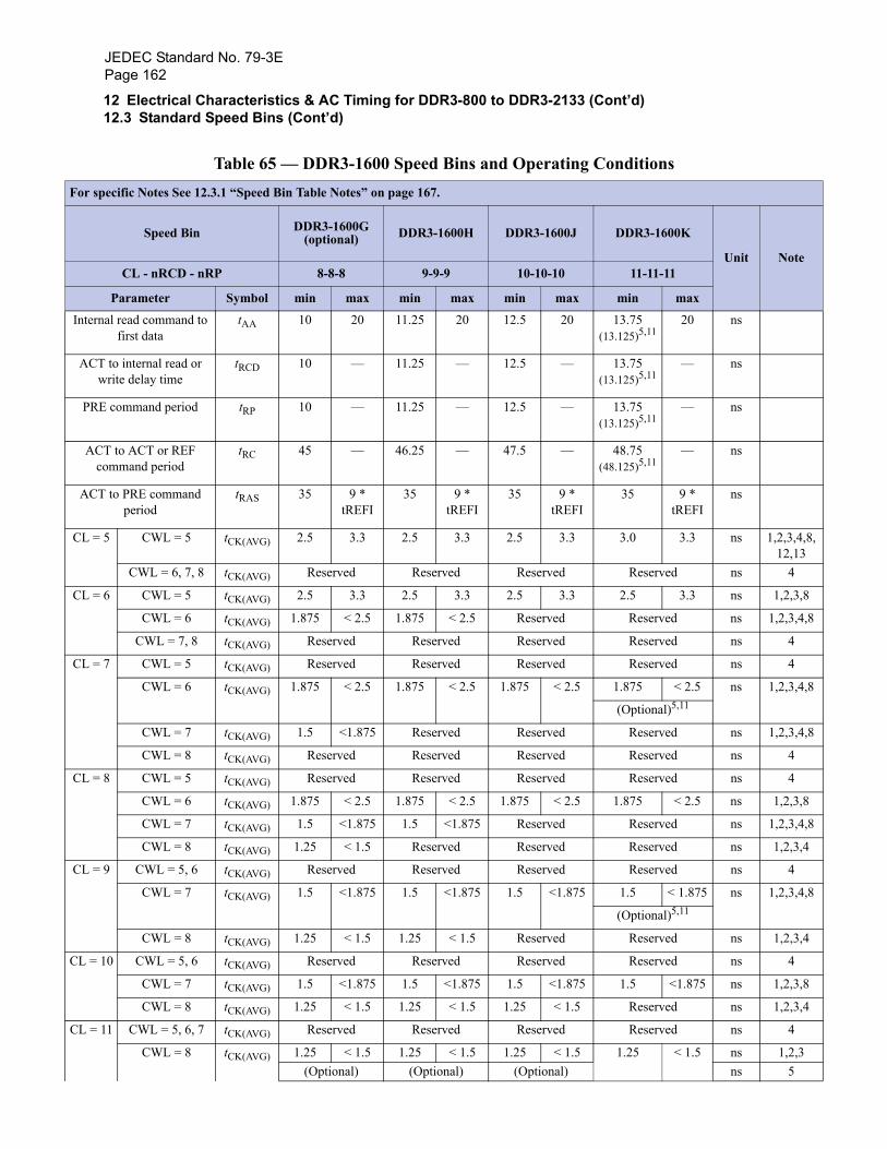
JEDEC Standard No. 79-3EPage 162
For
e
Inte
AC
PR
A
AC
CL ,8,3
CL ,8
4,8
CL
4,8
4,8
CL
,8
4,8
,4
CL
4,8
,4
CL =
,8
,4
CL =
3
12 Electrical Characteristics & AC Timing for DDR3-800 to DDR3-2133 (Cont’d)12.3 Standard Speed Bins (Cont’d)
Table 65 — DDR3-1600 Speed Bins and Operating Conditionsspecific Notes See 12.3.1 “Speed Bin Table Notes” on page 167.
Speed Bin DDR3-1600G (optional) DDR3-1600H DDR3-1600J DDR3-1600K
Unit NotCL - nRCD - nRP 8-8-8 9-9-9 10-10-10 11-11-11
Parameter Symbol min max min max min max min max
rnal read command to first data
tAA 10 20 11.25 20 12.5 20 13.75(13.125)5,11
20 ns
T to internal read or write delay time
tRCD 10 — 11.25 — 12.5 — 13.75(13.125)5,11
— ns
E command period tRP 10 — 11.25 — 12.5 — 13.75(13.125)5,11
— ns
CT to ACT or REF command period
tRC 45 — 46.25 — 47.5 — 48.75(48.125)5,11
— ns
T to PRE command period
tRAS 35 9 * tREFI
35 9 * tREFI
35 9 * tREFI
35 9 * tREFI
ns
= 5 CWL = 5 tCK(AVG) 2.5 3.3 2.5 3.3 2.5 3.3 3.0 3.3 ns 1,2,3,412,1
CWL = 6, 7, 8 tCK(AVG) Reserved Reserved Reserved Reserved ns 4
= 6 CWL = 5 tCK(AVG) 2.5 3.3 2.5 3.3 2.5 3.3 2.5 3.3 ns 1,2,3
CWL = 6 tCK(AVG) 1.875 < 2.5 1.875 < 2.5 Reserved Reserved ns 1,2,3,
CWL = 7, 8 tCK(AVG) Reserved Reserved Reserved Reserved ns 4
= 7 CWL = 5 tCK(AVG) Reserved Reserved Reserved Reserved ns 4
CWL = 6 tCK(AVG) 1.875 < 2.5 1.875 < 2.5 1.875 < 2.5 1.875 < 2.5 ns 1,2,3,
(Optional)5,11
CWL = 7 tCK(AVG) 1.5 <1.875 Reserved Reserved Reserved ns 1,2,3,
CWL = 8 tCK(AVG) Reserved Reserved Reserved Reserved ns 4
= 8 CWL = 5 tCK(AVG) Reserved Reserved Reserved Reserved ns 4
CWL = 6 tCK(AVG) 1.875 < 2.5 1.875 < 2.5 1.875 < 2.5 1.875 < 2.5 ns 1,2,3
CWL = 7 tCK(AVG) 1.5 <1.875 1.5 <1.875 Reserved Reserved ns 1,2,3,
CWL = 8 tCK(AVG) 1.25 < 1.5 Reserved Reserved Reserved ns 1,2,3
= 9 CWL = 5, 6 tCK(AVG) Reserved Reserved Reserved Reserved ns 4
CWL = 7 tCK(AVG) 1.5 <1.875 1.5 <1.875 1.5 <1.875 1.5 < 1.875 ns 1,2,3,
(Optional)5,11
CWL = 8 tCK(AVG) 1.25 < 1.5 1.25 < 1.5 Reserved Reserved ns 1,2,3
10 CWL = 5, 6 tCK(AVG) Reserved Reserved Reserved Reserved ns 4
CWL = 7 tCK(AVG) 1.5 <1.875 1.5 <1.875 1.5 <1.875 1.5 <1.875 ns 1,2,3
CWL = 8 tCK(AVG) 1.25 < 1.5 1.25 < 1.5 1.25 < 1.5 Reserved ns 1,2,3
11 CWL = 5, 6, 7 tCK(AVG) Reserved Reserved Reserved Reserved ns 4
CWL = 8 tCK(AVG) 1.25 < 1.5 1.25 < 1.5 1.25 < 1.5 1.25 < 1.5 ns 1,2,(Optional) (Optional) (Optional) ns 5
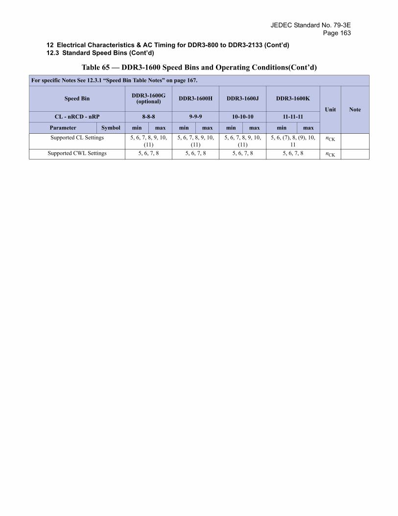
JEDEC Standard No. 79-3EPage 163
For
e
12 Electrical Characteristics & AC Timing for DDR3-800 to DDR3-2133 (Cont’d)12.3 Standard Speed Bins (Cont’d)
Supported CL Settings 5, 6, 7, 8, 9, 10, (11)
5, 6, 7, 8, 9, 10, (11)
5, 6, 7, 8, 9, 10, (11)
5, 6, (7), 8, (9), 10, 11
nCK
Supported CWL Settings 5, 6, 7, 8 5, 6, 7, 8 5, 6, 7, 8 5, 6, 7, 8 nCK
Table 65 — DDR3-1600 Speed Bins and Operating Conditions(Cont’d)specific Notes See 12.3.1 “Speed Bin Table Notes” on page 167.
Speed Bin DDR3-1600G (optional) DDR3-1600H DDR3-1600J DDR3-1600K
Unit NotCL - nRCD - nRP 8-8-8 9-9-9 10-10-10 11-11-11
Parameter Symbol min max min max min max min max
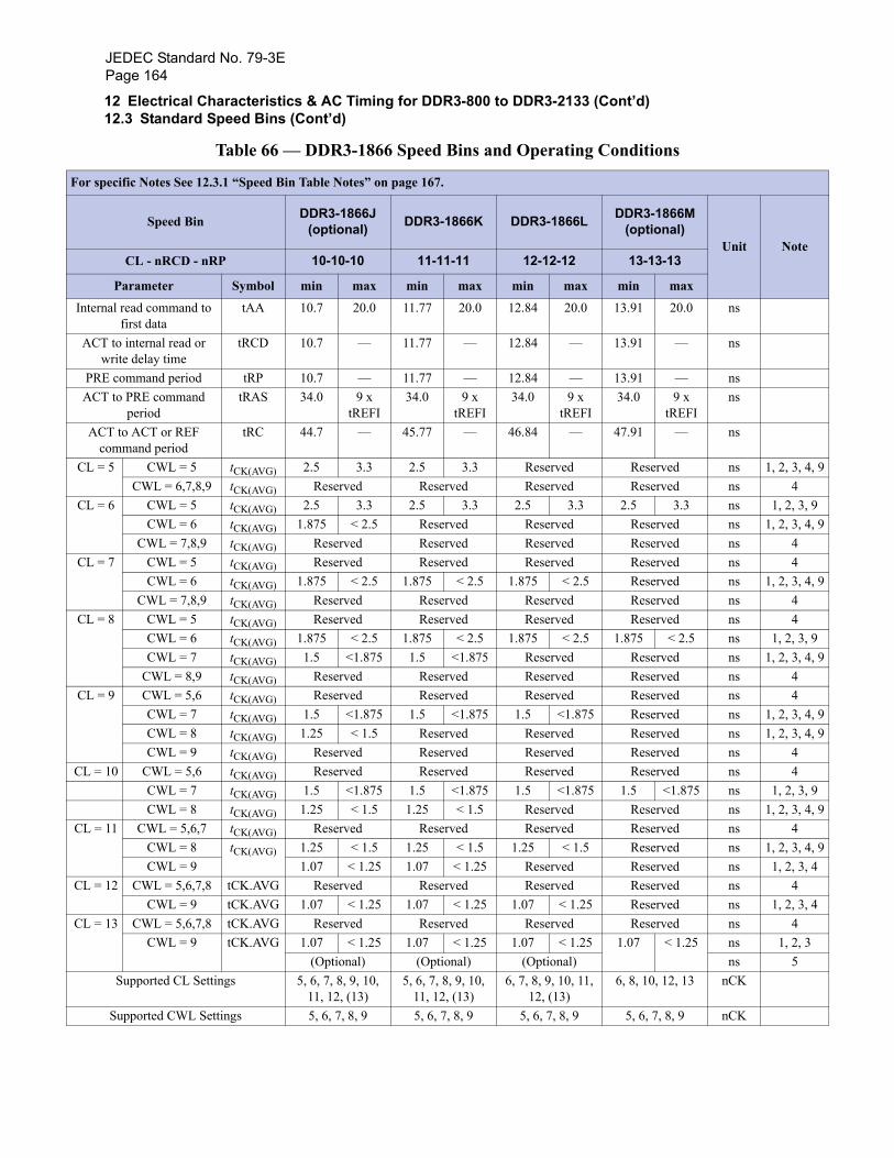
JEDEC Standard No. 79-3EPage 164
For
Inte
AC
PAC
A
CL 4, 9
CL , 94, 9
CL4, 9
CL, 94, 9
CL4, 94, 9
CL , 94, 9
CL 4, 9, 4
CL , 4
CL 3
12 Electrical Characteristics & AC Timing for DDR3-800 to DDR3-2133 (Cont’d)12.3 Standard Speed Bins (Cont’d)
Table 66 — DDR3-1866 Speed Bins and Operating Conditions
specific Notes See 12.3.1 “Speed Bin Table Notes” on page 167.
Speed Bin DDR3-1866J (optional) DDR3-1866K DDR3-1866L DDR3-1866M
(optional)Unit Note
CL - nRCD - nRP 10-10-10 11-11-11 12-12-12 13-13-13
Parameter Symbol min max min max min max min max
rnal read command to first data
tAA 10.7 20.0 11.77 20.0 12.84 20.0 13.91 20.0 ns
T to internal read or write delay time
tRCD 10.7 — 11.77 — 12.84 — 13.91 — ns
RE command period tRP 10.7 — 11.77 — 12.84 — 13.91 — nsT to PRE command
periodtRAS 34.0 9 x
tREFI34.0 9 x
tREFI34.0 9 x
tREFI34.0 9 x
tREFIns
CT to ACT or REF command period
tRC 44.7 — 45.77 — 46.84 — 47.91 — ns
= 5 CWL = 5 tCK(AVG) 2.5 3.3 2.5 3.3 Reserved Reserved ns 1, 2, 3, CWL = 6,7,8,9 tCK(AVG) Reserved Reserved Reserved Reserved ns 4
= 6 CWL = 5 tCK(AVG) 2.5 3.3 2.5 3.3 2.5 3.3 2.5 3.3 ns 1, 2, 3CWL = 6 tCK(AVG) 1.875 < 2.5 Reserved Reserved Reserved ns 1, 2, 3,
CWL = 7,8,9 tCK(AVG) Reserved Reserved Reserved Reserved ns 4 = 7 CWL = 5 tCK(AVG) Reserved Reserved Reserved Reserved ns 4
CWL = 6 tCK(AVG) 1.875 < 2.5 1.875 < 2.5 1.875 < 2.5 Reserved ns 1, 2, 3, CWL = 7,8,9 tCK(AVG) Reserved Reserved Reserved Reserved ns 4
= 8 CWL = 5 tCK(AVG) Reserved Reserved Reserved Reserved ns 4CWL = 6 tCK(AVG) 1.875 < 2.5 1.875 < 2.5 1.875 < 2.5 1.875 < 2.5 ns 1, 2, 3CWL = 7 tCK(AVG) 1.5 <1.875 1.5 <1.875 Reserved Reserved ns 1, 2, 3,
CWL = 8,9 tCK(AVG) Reserved Reserved Reserved Reserved ns 4 = 9 CWL = 5,6 tCK(AVG) Reserved Reserved Reserved Reserved ns 4
CWL = 7 tCK(AVG) 1.5 <1.875 1.5 <1.875 1.5 <1.875 Reserved ns 1, 2, 3, CWL = 8 tCK(AVG) 1.25 < 1.5 Reserved Reserved Reserved ns 1, 2, 3, CWL = 9 tCK(AVG) Reserved Reserved Reserved Reserved ns 4
= 10 CWL = 5,6 tCK(AVG) Reserved Reserved Reserved Reserved ns 4CWL = 7 tCK(AVG) 1.5 <1.875 1.5 <1.875 1.5 <1.875 1.5 <1.875 ns 1, 2, 3CWL = 8 tCK(AVG) 1.25 < 1.5 1.25 < 1.5 Reserved Reserved ns 1, 2, 3,
= 11 CWL = 5,6,7 tCK(AVG) Reserved Reserved Reserved Reserved ns 4CWL = 8 tCK(AVG) 1.25 < 1.5 1.25 < 1.5 1.25 < 1.5 Reserved ns 1, 2, 3, CWL = 9 1.07 < 1.25 1.07 < 1.25 Reserved Reserved ns 1, 2, 3
= 12 CWL = 5,6,7,8 tCK.AVG Reserved Reserved Reserved Reserved ns 4CWL = 9 tCK.AVG 1.07 < 1.25 1.07 < 1.25 1.07 < 1.25 Reserved ns 1, 2, 3
= 13 CWL = 5,6,7,8 tCK.AVG Reserved Reserved Reserved Reserved ns 4CWL = 9 tCK.AVG 1.07 < 1.25 1.07 < 1.25 1.07 < 1.25 1.07 < 1.25 ns 1, 2,
(Optional) (Optional) (Optional) ns 5Supported CL Settings 5, 6, 7, 8, 9, 10,
11, 12, (13)5, 6, 7, 8, 9, 10,
11, 12, (13)6, 7, 8, 9, 10, 11,
12, (13)6, 8, 10, 12, 13 nCK
Supported CWL Settings 5, 6, 7, 8, 9 5, 6, 7, 8, 9 5, 6, 7, 8, 9 5, 6, 7, 8, 9 nCK
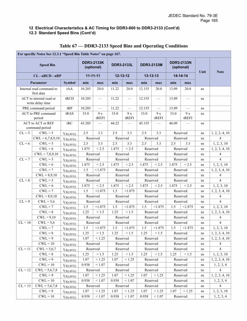
JEDEC Standard No. 79-3EPage 165
For s
e
Inte
AC
PRAC
A
CL = 4, 10
CL = , 104, 10
CL =, 104, 10
CL =, 104, 10
CL =, 104, 10
CL =, 104, 104, 10
CL =, 104, 10, 4
CL =4, 10, 4
CL =, 10, 4
12 Electrical Characteristics & AC Timing for DDR3-800 to DDR3-2133 (Cont’d)12.3 Standard Speed Bins (Cont’d)
Table 67 — DDR3-2133 Speed Bins and Operating Conditionspecific Notes See 12.3.1 “Speed Bin Table Notes” on page 167.
Speed Bin DDR3-2133K (optional) DDR3-2133L DDR3-2133M DDR3-2133N
(optional)Unit Not
CL - nRCD - nRP 11-11-11 12-12-12 13-13-13 14-14-14
Parameter Symbol min max min max min max min max
rnal read command to first data
tAA 10.285 20.0 11.22 20.0 12.155 20.0 13.09 20.0 ns
T to internal read or write delay time
tRCD 10.285 — 11.22 — 12.155 — 13.09 — ns
E command period tRP 10.285 — 11.22 — 12.155 — 13.09 — nsT to PRE command
periodtRAS 33.0 9 x
tREFI33.0 9 x
tREFI33.0 9 x
tREFI33.0 9 x
tREFIns
CT to ACT or REF command period
tRC 43.285 — 44.22 — 45.155 — 46.09 — ns
5 CWL = 5 tCK(AVG) 2.5 3.3 2.5 3.3 2.5 3.3 Reserved ns 1, 2, 3, CWL = 6,7,8,9,10 tCK(AVG) Reserved Reserved Reserved Reserved ns 4
6 CWL = 5 tCK(AVG) 2.5 3.3 2.5 3.3 2.5 3.3 2.5 3.3 ns 1, 2, 3CWL = 6 tCK(AVG) 1.875 < 2.5 1.875 < 2.5 Reserved Reserved ns 1, 2, 3,
CWL = 7,8,9,10 tCK(AVG) Reserved Reserved Reserved Reserved ns 4 7 CWL = 5 tCK(AVG) Reserved Reserved Reserved Reserved ns 4
CWL = 6 tCK(AVG) 1.875 < 2.5 1.875 < 2.5 1.875 < 2.5 1.875 < 2.5 ns 1, 2, 3CWL = 7 tCK(AVG) 1.5 < 1.875 Reserved Reserved Reserved ns 1, 2, 3,
CWL = 8,9,10 tCK(AVG) Reserved Reserved Reserved Reserved ns 4 8 CWL = 5 tCK(AVG) Reserved Reserved Reserved Reserved ns 4
CWL = 6 tCK(AVG) 1.875 < 2.5 1.875 < 2.5 1.875 < 2.5 1.875 < 2.5 ns 1, 2, 3CWL = 7 tCK(AVG) 1.5 <1.875 1.5 <1.875 Reserved Reserved ns 1, 2, 3,
CWL = 8,9,10 tCK(AVG) Reserved Reserved Reserved Reserved ns 4 9 CWL = 5,6 tCK(AVG) Reserved Reserved Reserved Reserved ns 4
CWL = 7 tCK(AVG) 1.5 <1.875 1.5 <1.875 1.5 <1.875 1.5 <1.875 ns 1, 2, 3CWL = 8 tCK(AVG) 1.25 < 1.5 1.25 < 1.5 Reserved Reserved ns 1, 2, 3,
CWL = 9,10 tCK(AVG) Reserved Reserved Reserved Reserved ns 4 10 CWL = 5,6 tCK(AVG) Reserved Reserved Reserved Reserved ns 4
CWL = 7 tCK(AVG) 1.5 <1.875 1.5 <1.875 1.5 <1.875 1.5 <1.875 ns 1, 2, 3CWL = 8 tCK(AVG) 1.25 < 1.5 1.25 < 1.5 1.25 < 1.5 Reserved ns 1, 2, 3, CWL = 9 tCK(AVG) 1.07 < 1.25 Reserved Reserved Reserved ns 1, 2, 3, CWL = 10 tCK(AVG) Reserved Reserved Reserved Reserved ns 4
11 CWL = 5,6,7 tCK(AVG) Reserved Reserved Reserved Reserved ns 4CWL = 8 tCK(AVG) 1.25 < 1.5 1.25 < 1.5 1.25 < 1.5 1.25 < 1.5 ns 1, 2, 3CWL = 9 tCK(AVG) 1.07 < 1.25 1.07 < 1.25 Reserved Reserved ns 1, 2, 3, CWL = 10 tCK(AVG) 0.938 < 1.07 Reserved Reserved Reserved ns 1, 2, 3
12 CWL = 5,6,7,8 tCK(AVG) Reserved Reserved Reserved Reserved ns 4CWL = 9 tCK(AVG) 1.07 < 1.25 1.07 < 1.25 1.07 < 1.25 Reserved ns 1, 2, 3, CWL = 10 tCK(AVG) 0.938 < 1.07 0.938 < 1.07 Reserved Reserved ns 1, 2, 3
13 CWL = 5,6,7,8 tCK(AVG) Reserved Reserved Reserved Reserved ns 4CWL = 9 tCK(AVG) 1.07 < 1.25 1.07 < 1.25 1.07 < 1.25 1.07 < 1.25 ns 1, 2, 3CWL = 10 tCK(AVG) 0.938 < 1.07 0.938 < 1.07 0.938 < 1.07 Reserved ns 1, 2, 3
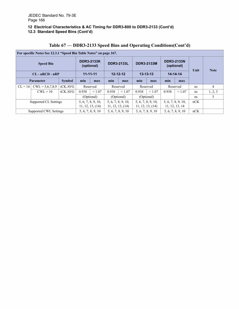
JEDEC Standard No. 79-3EPage 166
CL = 3
For s
e
12 Electrical Characteristics & AC Timing for DDR3-800 to DDR3-2133 (Cont’d)12.3 Standard Speed Bins (Cont’d)
14 CWL = 5,6,7,8,9 tCK.AVG Reserved Reserved Reserved Reserved ns 4CWL = 10 tCK.AVG 0.938 < 1.07 0.938 < 1.07 0.938 < 1.07 0.938 < 1.07 ns 1, 2,
(Optional) (Optional) (Optional) ns 5Supported CL Settings 5, 6, 7, 8, 9, 10,
11, 12, 13, (14)5, 6, 7, 8, 9, 10, 11, 12, 13, (14)
5, 6, 7, 8, 9, 10, 11, 12, 13, (14)
5, 6, 7, 8, 9, 10, 11, 12, 13, 14
nCK
Supported CWL Settings 5, 6, 7, 8, 9, 10 5, 6, 7, 8, 9, 10 5, 6, 7, 8, 9, 10 5, 6, 7, 8, 9, 10 nCK
Table 67 — DDR3-2133 Speed Bins and Operating Conditions(Cont’d)pecific Notes See 12.3.1 “Speed Bin Table Notes” on page 167.
Speed Bin DDR3-2133K (optional) DDR3-2133L DDR3-2133M DDR3-2133N
(optional)Unit Not
CL - nRCD - nRP 11-11-11 12-12-12 13-13-13 14-14-14
Parameter Symbol min max min max min max min max
JEDEC Standard No. 79-3EPage 167
12 Electrical Characteristics & AC Timing for DDR3-800 to DDR3-2133 (Cont’d)12.3 Standard Speed Bins (Cont’d)
12.3.1 Speed Bin Table Notes
Absolute Specification (TOPER; VDDQ = VDD = 1.5V +/- 0.075 V);
NOTE 1. The CL setting and CWL setting result in tCK(AVG).MIN and tCK(AVG).MAX requirements.When making a selection of tCK(AVG), both need to be fulfilled: Requirements from CL settingas well as requirements from CWL setting.
NOTE 2. tCK(AVG).MIN limits: Since CAS Latency is not purely analog - data and strobe output are syn-chronized by the DLL - all possible intermediate frequencies may not be guaranteed. An applica-tion should use the next smaller JEDEC standard tCK(AVG) value (3.0, 2.5, 1.875, 1.5, 1.25,1.07, or 0.938 ns) when calculating CL [nCK] = tAA [ns] / tCK(AVG) [ns], rounding up to thenext ‘Supported CL’, where tCK(AVG) = 3.0 ns should only be used for CL = 5 calculation.
NOTE 3. tCK(AVG).MAX limits: Calculate tCK(AVG) = tAA.MAX / CL SELECTED and round theresulting tCK(AVG) down to the next valid speed bin (i.e. 3.3ns or 2.5ns or 1.875 ns or 1.5 ns or1.25 ns or 1.07 ns or 0.938 ns). This result is tCK(AVG).MAX corresponding to CLSELECTED.
NOTE 4. ‘Reserved’ settings are not allowed. User must program a different value.NOTE 5. ‘Optional’ settings allow certain devices in the industry to support this setting, however, it is not
a mandatory feature. Refer to supplier’s data sheet and/or the DIMM SPD information if andhow this setting is supported.
NOTE 6. Any DDR3-1066 speed bin also supports functional operation at lower frequencies as shown inthe table which are not subject to Production Tests but verified by Design/Characterization.
NOTE 7. Any DDR3-1333 speed bin also supports functional operation at lower frequencies as shown inthe table which are not subject to Production Tests but verified by Design/Characterization.
NOTE 8. Any DDR3-1600 speed bin also supports functional operation at lower frequencies as shown inthe table which are not subject to Production Tests but verified by Design/Characterization.
NOTE 9. Any DDR3-1866 speed bin also supports functional operation at lower frequencies as shown inthe table which are not subject to Production Tests but verified by Design/Characterization.
NOTE 10.Any DDR3-2133 speed bin also supports functional operation at lower frequencies as shown inthe table which are not subject to Production Tests but verified by Design/Characterization.
NOTE 11.For devices supporting optional down binning to CL=7 and CL=9, tAA/tRCD/tRPmin must be13.125 ns or lower. SPD settings must be programmed to match. For example, DDR3-1333Hdevices supporting down binning to DDR3-1066F should program 13.125 ns in SPD bytes fortAAmin (Byte 16), tRCDmin (Byte 18), and tRPmin (Byte 20). DDR3-1600K devices support-ing down binning to DDR3-1333H or DDR3-1066F should program 13.125 ns in SPD bytes fortAAmin (Byte16), tRCDmin (Byte 18), and tRPmin (Byte 20). Once tRP (Byte 20) is pro-grammed to 13.125ns, tRCmin (Byte 21,23) also should be programmed accodingly. For exam-ple, 49.125ns (tRASmin + tRPmin = 36 ns + 13.125 ns) for DDR3-1333H and 48.125ns(tRASmin + tRPmin = 35 ns + 13.125 ns) for DDR3-1600K.
NOTE 12.DDR3 800 AC timing apply if DRAM operates at lower than 800 MT/s data rate.NOTE 13.For CL5 support, refer to DIMM SPD information. DRAM is required to support CL5. CL5 is
not mandatory in SPD coding.

JEDEC Standard No. 79-3EPage 168
This page left blank.
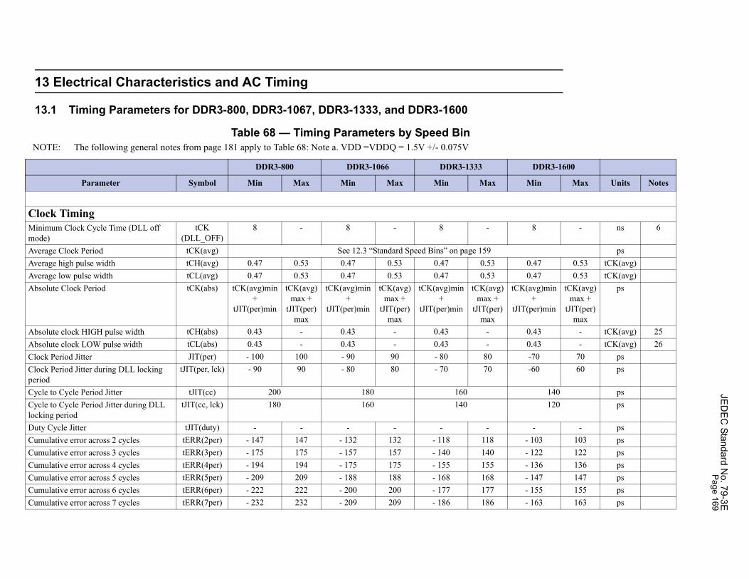
JED
EC
Standard No. 79-3EPage 169
13 E
13.1
NOTE:
DDR3-1600
Min Max Units Notes
Clock TMinimummode)
8 - ns 6
Average C psAverage h 0.47 0.53 tCK(avg)Average l 0.47 0.53 tCK(avg)Absolute K(avg)min
+ T(per)min
tCK(avg)max +
tJIT(per)max
ps
Absolute 0.43 - tCK(avg) 25Absolute 0.43 - tCK(avg) 26Clock Per -70 70 psClock Perperiod
-60 60 ps
Cycle to C 140 psCycle to Clocking p
120 ps
Duty Cyc - - psCumulati - 103 103 psCumulati - 122 122 psCumulati - 136 136 psCumulati - 147 147 psCumulati - 155 155 psCumulati - 163 163 ps
lectrical Characteristics and AC Timing
Timing Parameters for DDR3-800, DDR3-1067, DDR3-1333, and DDR3-1600
Table 68 — Timing Parameters by Speed Bin The following general notes from page 181 apply to Table 68: Note a. VDD =VDDQ = 1.5V +/- 0.075V
DDR3-800 DDR3-1066 DDR3-1333
Parameter Symbol Min Max Min Max Min Max
iming Clock Cycle Time (DLL off tCK
(DLL_OFF)8 - 8 - 8 -
lock Period tCK(avg) See 12.3 “Standard Speed Bins” on page 159igh pulse width tCH(avg) 0.47 0.53 0.47 0.53 0.47 0.53ow pulse width tCL(avg) 0.47 0.53 0.47 0.53 0.47 0.53Clock Period tCK(abs) tCK(avg)min
+ tJIT(per)min
tCK(avg)max +
tJIT(per)max
tCK(avg)min +
tJIT(per)min
tCK(avg)max +
tJIT(per)max
tCK(avg)min +
tJIT(per)min
tCK(avg)max +
tJIT(per)max
tC
tJI
clock HIGH pulse width tCH(abs) 0.43 - 0.43 - 0.43 -clock LOW pulse width tCL(abs) 0.43 - 0.43 - 0.43 -iod Jitter JIT(per) - 100 100 - 90 90 - 80 80iod Jitter during DLL locking tJIT(per, lck) - 90 90 - 80 80 - 70 70
ycle Period Jitter tJIT(cc) 200 180 160ycle Period Jitter during DLL
eriodtJIT(cc, lck) 180 160 140
le Jitter tJIT(duty) - - - - - -ve error across 2 cycles tERR(2per) - 147 147 - 132 132 - 118 118ve error across 3 cycles tERR(3per) - 175 175 - 157 157 - 140 140ve error across 4 cycles tERR(4per) - 194 194 - 175 175 - 155 155ve error across 5 cycles tERR(5per) - 209 209 - 188 188 - 168 168ve error across 6 cycles tERR(6per) - 222 222 - 200 200 - 177 177ve error across 7 cycles tERR(7per) - 232 232 - 209 209 - 186 186

JED
EC
Standard No. 79-3E
Page 170
Cumulativ - 169 169 psCumulativ - 175 175 psCumulativ - 180 180 psCumulativ - 184 184 psCumulativ - 188 188 psCumulativ50 cycles
ps 24
Data TDQS, DQaccess
- 100 ps 13
DQ outpu 0.38 - tCK(avg) 13, gDQ low-i - 450 225 ps 13, 14, fDQ high i - 225 ps 13, 14, fData setupto Vih(ac)
- ps d, 17
Data setupto Vih(ac)
10 ps d, 17
Data holdreferenced
45 ps d, 17
DQ and Dinput
360 - ps 28
Data SDQS,DQS 0.9 Note 19 tCK(avg) 13, 19, gDQS, DQ 0.3 Note 11 tCK(avg) 11, 13, gDQS, DQ 0.40 - tCK(avg) 13, gDQS, DQ 0.40 - tCK(avg) 13, gDQS, DQ 0.9 - tCK(avg) 1DQS, DQPostamble
0.3 - tCK(avg) 1
DQS, DQtime from
- 225 225 ps 13, f
NOTE:
DDR3-1600
Min Max Units Notes
13Electrical C
haracteristics and AC
Timing (C
ont’d)13.1 Tim
ing Parameters for D
DR
3-800, DD
R3-1067, D
DR
3-1333, and DD
R3-1600 (C
ont’d
e error across 8 cycles tERR(8per) - 241 241 - 217 217 - 193 193e error across 9 cycles tERR(9per) - 249 249 - 224 224 - 200 200e error across 10 cycles tERR(10per) - 257 257 - 231 231 - 205 205e error across 11 cycles tERR(11per) - 263 263 - 237 237 - 210 210e error across 12 cycles tERR(12per) - 269 269 - 242 242 - 215 215e error across n = 13, 14 . . . 49, tERR(nper) tERR(nper)min = (1 + 0.68ln(n)) * tJIT(per)min
tERR(nper)max = (1 + 0.68ln(n)) * tJIT(per)max
imingS# to DQ skew, per group, per tDQSQ - 200 - 150 - 125
t hold time from DQS, DQS# tQH 0.38 - 0.38 - 0.38 -mpedance time from CK, CK# tLZ(DQ) - 800 400 - 600 300 - 500 250mpedance time from CK, CK# tHZ(DQ) - 400 - 300 - 250 time to DQS, DQS# referenced / Vil(ac) levels
tDS(base) AC175
75 25 -
time to DQS, DQS# referenced / Vil(ac) levels
tDS(base) AC150
125 75 30
time from DQS, DQS# to Vih(dc) / Vil(dc) levels
tDH(base) DC100
150 100 65
M Input pulse width for each tDIPW 600 - 490 - 400 -
trobe Timing# differential READ Preamble tRPRE 0.9 Note 19 0.9 Note 19 0.9 Note 19
S# differential READ Postamble tRPST 0.3 Note 11 0.3 Note 11 0.3 Note 11S# differential output high time tQSH 0.38 - 0.38 - 0.40 -S# differential output low time tQSL 0.38 - 0.38 - 0.40 -S# differential WRITE Preamble tWPRE 0.9 - 0.9 - 0.9 -S# differential WRITE tWPST 0.3 - 0.3 - 0.3 -
S# rising edge output access rising CK, CK#
tDQSCK - 400 400 - 300 300 - 255 255
Table 68 — Timing Parameters by Speed Bin (Cont’d)The following general notes from page 181 apply to Table 68: Note a. VDD =VDDQ = 1.5V +/- 0.075V
DDR3-800 DDR3-1066 DDR3-1333
Parameter Symbol Min Max Min Max Min Max
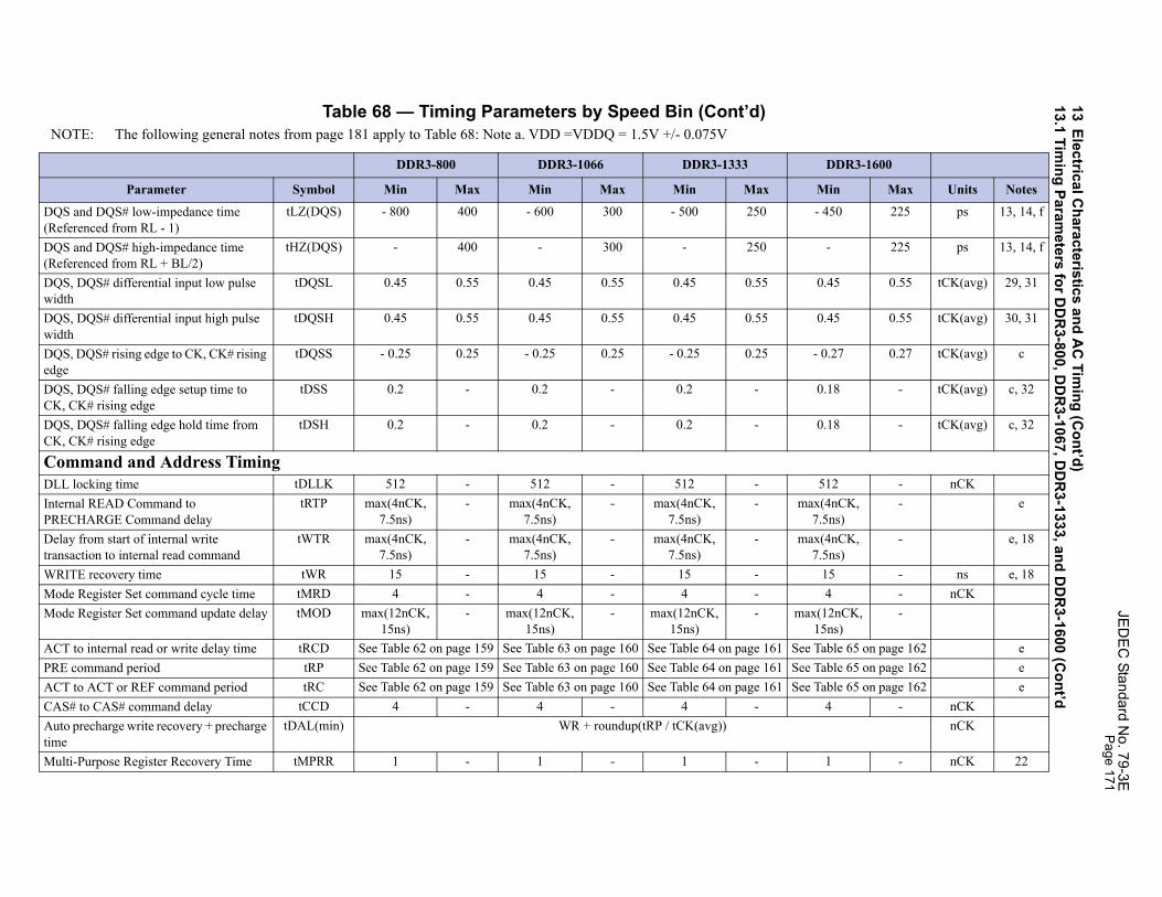
JED
EC
Standard No. 79-3EPage 171
DQS and (Referenc
- 450 225 ps 13, 14, f
DQS and (Referenc
- 225 ps 13, 14, f
DQS, DQwidth
0.45 0.55 tCK(avg) 29, 31
DQS, DQwidth
0.45 0.55 tCK(avg) 30, 31
DQS, DQedge
- 0.27 0.27 tCK(avg) c
DQS, DQCK, CK#
0.18 - tCK(avg) c, 32
DQS, DQCK, CK#
0.18 - tCK(avg) c, 32
CommDLL lock 512 - nCKInternal RPRECHA
ax(4nCK, 7.5ns)
- e
Delay frotransactio
ax(4nCK, 7.5ns)
- e, 18
WRITE r 15 - ns e, 18Mode Reg 4 - nCKMode Reg x(12nCK,
15ns)-
ACT to in Table 65 on page 162 ePRE com Table 65 on page 162 eACT to A Table 65 on page 162 eCAS# to 4 - nCKAuto prectime
nCK
Multi-Pur 1 - nCK 22
NOTE:
DDR3-1600
Min Max Units Notes
13Electrical C
haracteristics and AC
Timing (C
ont’d)13.1 Tim
ing Parameters for D
DR
3-800, DD
R3-1067, D
DR
3-1333, and DD
R3-1600 (C
ont’d
DQS# low-impedance time ed from RL - 1)
tLZ(DQS) - 800 400 - 600 300 - 500 250
DQS# high-impedance time ed from RL + BL/2)
tHZ(DQS) - 400 - 300 - 250
S# differential input low pulse tDQSL 0.45 0.55 0.45 0.55 0.45 0.55
S# differential input high pulse tDQSH 0.45 0.55 0.45 0.55 0.45 0.55
S# rising edge to CK, CK# rising tDQSS - 0.25 0.25 - 0.25 0.25 - 0.25 0.25
S# falling edge setup time to rising edge
tDSS 0.2 - 0.2 - 0.2 -
S# falling edge hold time from rising edge
tDSH 0.2 - 0.2 - 0.2 -
and and Address Timinging time tDLLK 512 - 512 - 512 -EAD Command to RGE Command delay
tRTP max(4nCK, 7.5ns)
- max(4nCK, 7.5ns)
- max(4nCK, 7.5ns)
- m
m start of internal write n to internal read command
tWTR max(4nCK, 7.5ns)
- max(4nCK, 7.5ns)
- max(4nCK, 7.5ns)
- m
ecovery time tWR 15 - 15 - 15 -ister Set command cycle time tMRD 4 - 4 - 4 -ister Set command update delay tMOD max(12nCK,
15ns)- max(12nCK,
15ns)- max(12nCK,
15ns)- ma
ternal read or write delay time tRCD See Table 62 on page 159 See Table 63 on page 160 See Table 64 on page 161 Seemand period tRP See Table 62 on page 159 See Table 63 on page 160 See Table 64 on page 161 SeeCT or REF command period tRC See Table 62 on page 159 See Table 63 on page 160 See Table 64 on page 161 See
CAS# command delay tCCD 4 - 4 - 4 -harge write recovery + precharge tDAL(min) WR + roundup(tRP / tCK(avg))
pose Register Recovery Time tMPRR 1 - 1 - 1 -
Table 68 — Timing Parameters by Speed Bin (Cont’d)The following general notes from page 181 apply to Table 68: Note a. VDD =VDDQ = 1.5V +/- 0.075V
DDR3-800 DDR3-1066 DDR3-1333
Parameter Symbol Min Max Min Max Min Max
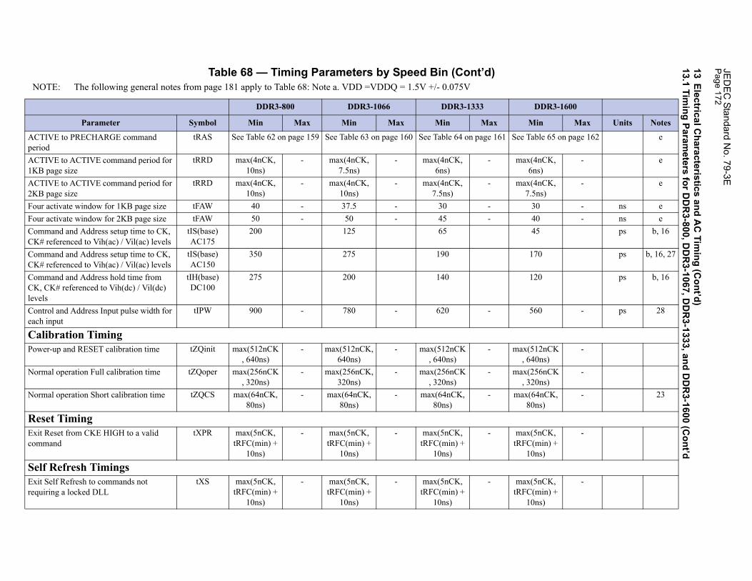
JED
EC
Standard No. 79-3E
Page 172
ACTIVE period
Table 65 on page 162 e
ACTIVE 1KB page
ax(4nCK, 6ns)
- e
ACTIVE 2KB page
ax(4nCK, 7.5ns)
- e
Four activ 30 - ns eFour activ 40 - ns eCommandCK# refer
45 ps b, 16
CommandCK# refer
170 ps b, 16, 27
CommandCK, CK#levels
120 ps b, 16
Control aneach inpu
560 - ps 28
CalibraPower-up x(512nCK
, 640ns)-
Normal o x(256nCK, 320ns)
-
Normal o x(64nCK, 80ns)
- 23
Reset TExit Resecommand
ax(5nCK, FC(min) +
10ns)
-
Self ReExit Self requiring
ax(5nCK, FC(min) +
10ns)
-
NOTE:
DDR3-1600
Min Max Units Notes
13Electrical C
haracteristics and AC
Timing (C
ont’d)13.1 Tim
ing Parameters for D
DR
3-800, DD
R3-1067, D
DR
3-1333, and DD
R3-1600 (C
ont’d
to PRECHARGE command tRAS See Table 62 on page 159 See Table 63 on page 160 See Table 64 on page 161 See
to ACTIVE command period for size
tRRD max(4nCK, 10ns)
- max(4nCK, 7.5ns)
- max(4nCK, 6ns)
- m
to ACTIVE command period for size
tRRD max(4nCK, 10ns)
- max(4nCK, 10ns)
- max(4nCK, 7.5ns)
- m
ate window for 1KB page size tFAW 40 - 37.5 - 30 -ate window for 2KB page size tFAW 50 - 50 - 45 - and Address setup time to CK, enced to Vih(ac) / Vil(ac) levels
tIS(base) AC175
200 125 65
and Address setup time to CK, enced to Vih(ac) / Vil(ac) levels
tIS(base) AC150
350 275 190
and Address hold time from referenced to Vih(dc) / Vil(dc)
tIH(base) DC100
275 200 140
d Address Input pulse width for t
tIPW 900 - 780 - 620 -
tion Timing and RESET calibration time tZQinit max(512nCK
, 640ns)- max(512nCK,
640ns)- max(512nCK
, 640ns)- ma
peration Full calibration time tZQoper max(256nCK, 320ns)
- max(256nCK, 320ns)
- max(256nCK, 320ns)
- ma
peration Short calibration time tZQCS max(64nCK, 80ns)
- max(64nCK, 80ns)
- max(64nCK, 80ns)
- ma
imingt from CKE HIGH to a valid tXPR max(5nCK,
tRFC(min) + 10ns)
- max(5nCK, tRFC(min) +
10ns)
- max(5nCK, tRFC(min) +
10ns)
- mtR
fresh TimingsRefresh to commands not a locked DLL
tXS max(5nCK, tRFC(min) +
10ns)
- max(5nCK, tRFC(min) +
10ns)
- max(5nCK, tRFC(min) +
10ns)
- mtR
Table 68 — Timing Parameters by Speed Bin (Cont’d)The following general notes from page 181 apply to Table 68: Note a. VDD =VDDQ = 1.5V +/- 0.075V
DDR3-800 DDR3-1066 DDR3-1333
Parameter Symbol Min Max Min Max Min Max

JED
EC
Standard No. 79-3EPage 173
Exit Self locked DL
LLK(min) - nCK
Minimumentry to e
KE(min) + 1 nCK
-
Valid CloRefresh EEntry (PD
ax(5 nCK, 10 ns)
-
Valid CloRefresh E(PDX) or
ax(5 nCK, 10 ns)
-
Power Exit Powevalid comDown wirequiring
ax(3nCK, 6ns)
-
Exit Prechfrozen to DLL
x(10nCK, 24ns)
- 2
CKE min ax(3nCK, 5ns)
-
Command 1 - nCKPower Do KE(min) 9 * tREFI 15Timing ofentry
1 - nCK 20
Timing ofPower Do
1 - nCK 20
Timing ofDown ent
L + 4 + 1 -nCK
Timing ofentry (BL
L + 4 + (tWR / K(avg))
- nCK 9
NOTE:
DDR3-1600
Min Max Units Notes
13Electrical C
haracteristics and AC
Timing (C
ont’d)13.1 Tim
ing Parameters for D
DR
3-800, DD
R3-1067, D
DR
3-1333, and DD
R3-1600 (C
ont’d
Refresh to commands requiring a L
tXSDLL tDLLK(min) - tDLLK(min) - tDLLK(min) - tD
CKE low width for Self Refresh xit timing
tCKESR tCKE(min) + 1 nCK
- tCKE(min) + 1 nCK
- tCKE(min) + 1 nCK
- tC
ck Requirement after Self ntry (SRE) or Power-Down E)
tCKSRE max(5 nCK, 10 ns)
- max(5 nCK, 10 ns)
- max(5 nCK, 10 ns)
- m
ck Requirement before Self xit (SRX) or Power-Down Exit Reset Exit
tCKSRX max(5 nCK, 10 ns)
- max(5 nCK, 10 ns)
- max(5 nCK, 10 ns)
- m
Down Timingsr Down with DLL on to any mand; Exit Precharge Power
th DLL frozen to commands not a locked DLL
tXP max(3nCK, 7.5ns)
- max(3nCK, 7.5ns)
- max(3nCK, 6ns)
- m
arge Power Down with DLL commands requiring a locked
tXPDLL max(10nCK, 24ns)
- max(10nCK, 24ns)
- max(10nCK, 24ns)
- ma
imum pulse width tCKE max(3nCK 7.5ns)
- max(3nCK, 5.625ns)
- max(3nCK, 5.625ns)
- m
pass disable delay tCPDED 1 - 1 - 1 -wn Entry to Exit Timing tPD tCKE(min) 9 * tREFI tCKE(min) 9 * tREFI tCKE(min) 9 * tREFI tC ACT command to Power Down tACTPDEN 1 - 1 - 1 -
PRE or PREA command to wn entry
tPRPDEN 1 - 1 - 1 -
RD/RDA command to Power ry
tRDPDEN RL + 4 + 1 - RL + 4 + 1 - RL + 4 + 1 - R
WR command to Power Down 8OTF, BL8MRS, BC4OTF)
tWRPDEN WL + 4 + (tWR /
tCK(avg))
- WL + 4 + (tWR /
tCK(avg))
- WL + 4 + (tWR /
tCK(avg))
- W
tC
Table 68 — Timing Parameters by Speed Bin (Cont’d)The following general notes from page 181 apply to Table 68: Note a. VDD =VDDQ = 1.5V +/- 0.075V
DDR3-800 DDR3-1066 DDR3-1333
Parameter Symbol Min Max Min Max Min Max
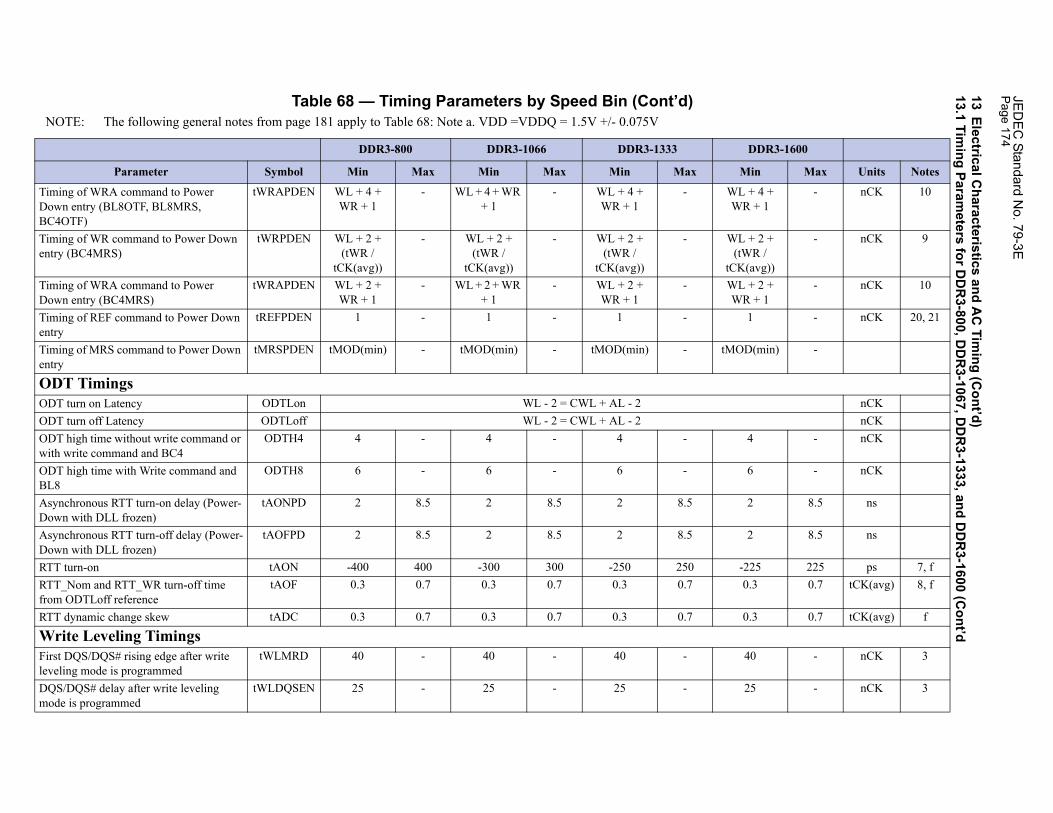
JED
EC
Standard No. 79-3E
Page 174
Timing ofDown entBC4OTF)
L + 4 + WR + 1
- nCK 10
Timing ofentry (BC
L + 2 + (tWR / K(avg))
- nCK 9
Timing ofDown ent
L + 2 + WR + 1
- nCK 10
Timing ofentry
1 - nCK 20, 21
Timing ofentry
OD(min) -
ODT TODT turn nCKODT turn nCKODT highwith write
4 - nCK
ODT highBL8
6 - nCK
AsynchroDown wit
2 8.5 ns
AsynchroDown wit
2 8.5 ns
RTT turn- -225 225 ps 7, fRTT_Nomfrom ODT
0.3 0.7 tCK(avg) 8, f
RTT dyna 0.3 0.7 tCK(avg) f
Write LFirst DQSleveling m
40 - nCK 3
DQS/DQSmode is p
25 - nCK 3
NOTE:
DDR3-1600
Min Max Units Notes
13Electrical C
haracteristics and AC
Timing (C
ont’d)13.1 Tim
ing Parameters for D
DR
3-800, DD
R3-1067, D
DR
3-1333, and DD
R3-1600 (C
ont’d
WRA command to Power ry (BL8OTF, BL8MRS,
tWRAPDEN WL + 4 + WR + 1
- WL + 4 + WR + 1
- WL + 4 + WR + 1
- W
WR command to Power Down 4MRS)
tWRPDEN WL + 2 + (tWR /
tCK(avg))
- WL + 2 + (tWR /
tCK(avg))
- WL + 2 + (tWR /
tCK(avg))
- W
tC WRA command to Power ry (BC4MRS)
tWRAPDEN WL + 2 + WR + 1
- WL + 2 + WR + 1
- WL + 2 + WR + 1
- W
REF command to Power Down tREFPDEN 1 - 1 - 1 -
MRS command to Power Down tMRSPDEN tMOD(min) - tMOD(min) - tMOD(min) - tM
imings on Latency ODTLon WL - 2 = CWL + AL - 2 off Latency ODTLoff WL - 2 = CWL + AL - 2 time without write command or command and BC4
ODTH4 4 - 4 - 4 -
time with Write command and ODTH8 6 - 6 - 6 -
nous RTT turn-on delay (Power-h DLL frozen)
tAONPD 2 8.5 2 8.5 2 8.5
nous RTT turn-off delay (Power-h DLL frozen)
tAOFPD 2 8.5 2 8.5 2 8.5
on tAON -400 400 -300 300 -250 250 and RTT_WR turn-off time Loff reference
tAOF 0.3 0.7 0.3 0.7 0.3 0.7
mic change skew tADC 0.3 0.7 0.3 0.7 0.3 0.7
eveling Timings/DQS# rising edge after write ode is programmed
tWLMRD 40 - 40 - 40 -
# delay after write leveling rogrammed
tWLDQSEN 25 - 25 - 25 -
Table 68 — Timing Parameters by Speed Bin (Cont’d)The following general notes from page 181 apply to Table 68: Note a. VDD =VDDQ = 1.5V +/- 0.075V
DDR3-800 DDR3-1066 DDR3-1333
Parameter Symbol Min Max Min Max Min Max
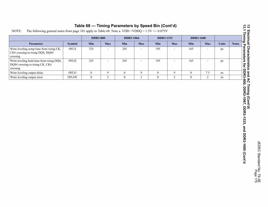
JED
EC
Standard No. 79-3EPage 175
Write levCK# croscrossing
165 - ps
Write leveDQS# crocrossing
165 - ps
Write lev 0 7.5 nsWrite lev 0 2 ns
NOTE:
DDR3-1600
Min Max Units Notes
13Electrical C
haracteristics and AC
Timing (C
ont’d)13.1 Tim
ing Parameters for D
DR
3-800, DD
R3-1067, D
DR
3-1333, and DD
R3-1600 (C
ont’d
eling setup time from rising CK, sing to rising DQS, DQS#
tWLS 325 - 245 - 195 -
ling hold time from rising DQS, ssing to rising CK, CK#
tWLH 325 - 245 - 195 -
eling output delay tWLO 0 9 0 9 0 9eling output error tWLOE 0 2 0 2 0 2
Table 68 — Timing Parameters by Speed Bin (Cont’d)The following general notes from page 181 apply to Table 68: Note a. VDD =VDDQ = 1.5V +/- 0.075V
DDR3-800 DDR3-1066 DDR3-1333
Parameter Symbol Min Max Min Max Min Max
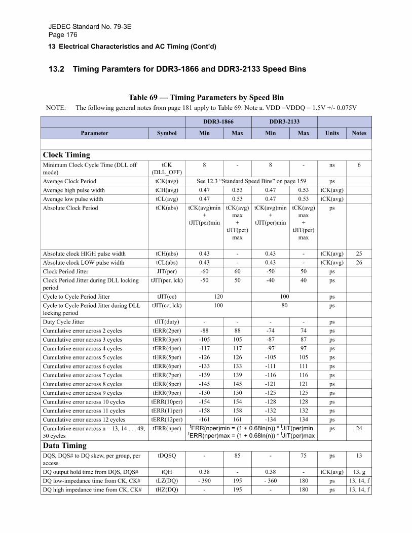
JEDEC Standard No. 79-3EPage 176
13 Electrical Characteristics and AC Timing (Cont’d)
13.2 Timing Paramters for DDR3-1866 and DDR3-2133 Speed Bins
Table 69 — Timing Parameters by Speed Bin NOTE: The following general notes from page 181 apply to Table 69: Note a. VDD =VDDQ = 1.5V +/- 0.075V
DDR3-1866 DDR3-2133
Parameter Symbol Min Max Min Max Units Notes
Clock TimingMinimum Clock Cycle Time (DLL off mode)
tCK (DLL_OFF)
8 - 8 - ns 6
Average Clock Period tCK(avg) See 12.3 “Standard Speed Bins” on page 159 psAverage high pulse width tCH(avg) 0.47 0.53 0.47 0.53 tCK(avg)Average low pulse width tCL(avg) 0.47 0.53 0.47 0.53 tCK(avg)Absolute Clock Period tCK(abs) tCK(avg)min
+tJIT(per)min
tCK(avg)max
+tJIT(per)
max
tCK(avg)min+
tJIT(per)min
tCK(avg)max
+tJIT(per)
max
ps
Absolute clock HIGH pulse width tCH(abs) 0.43 - 0.43 - tCK(avg) 25Absolute clock LOW pulse width tCL(abs) 0.43 - 0.43 - tCK(avg) 26Clock Period Jitter JIT(per) -60 60 -50 50 psClock Period Jitter during DLL locking period
tJIT(per, lck) -50 50 -40 40 ps
Cycle to Cycle Period Jitter tJIT(cc) 120 100 psCycle to Cycle Period Jitter during DLL locking period
tJIT(cc, lck) 100 80 ps
Duty Cycle Jitter tJIT(duty) - - - - psCumulative error across 2 cycles tERR(2per) -88 88 -74 74 psCumulative error across 3 cycles tERR(3per) -105 105 -87 87 psCumulative error across 4 cycles tERR(4per) -117 117 -97 97 psCumulative error across 5 cycles tERR(5per) -126 126 -105 105 psCumulative error across 6 cycles tERR(6per) -133 133 -111 111 psCumulative error across 7 cycles tERR(7per) -139 139 -116 116 psCumulative error across 8 cycles tERR(8per) -145 145 -121 121 psCumulative error across 9 cycles tERR(9per) -150 150 -125 125 psCumulative error across 10 cycles tERR(10per) -154 154 -128 128 psCumulative error across 11 cycles tERR(11per) -158 158 -132 132 psCumulative error across 12 cycles tERR(12per) -161 161 -134 134 psCumulative error across n = 13, 14 . . . 49, 50 cycles
tERR(nper) tERR(nper)min = (1 + 0.68ln(n)) * tJIT(per)mintERR(nper)max = (1 + 0.68ln(n)) * tJIT(per)max
ps 24
Data TimingDQS, DQS# to DQ skew, per group, per access
tDQSQ - 85 - 75 ps 13
DQ output hold time from DQS, DQS# tQH 0.38 - 0.38 - tCK(avg) 13, gDQ low-impedance time from CK, CK# tLZ(DQ) - 390 195 - 360 180 ps 13, 14, fDQ high impedance time from CK, CK# tHZ(DQ) - 195 - 180 ps 13, 14, f
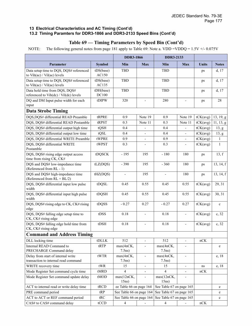
JEDEC Standard No. 79-3EPage 177
13 Electrical Characteristics and AC Timing (Cont’d)13.2 Timing Paramters for DDR3-1866 and DDR3-2133 Speed Bins (Cont’d)
Data setup time to DQS, DQS# referenced to Vih(ac) / Vil(ac) levels
tDS(base) AC150
TBD TBD ps d, 17
Data setup time to DQS, DQS# referenced to Vih(ac) / Vil(ac) levels
tDS(base) AC135
TBD TBD ps d, 17
Data hold time from DQS, DQS# referenced to Vih(dc) / Vil(dc) levels
tDH(base) DC100
TBD TBD ps d, 17
DQ and DM Input pulse width for each input
tDIPW 320 - 280 - ps 28
Data Strobe TimingDQS,DQS# differential READ Preamble tRPRE 0.9 Note 19 0.9 Note 19 tCK(avg) 13, 19, gDQS, DQS# differential READ Postamble tRPST 0.3 Note 11 0.3 Note 11 tCK(avg) 11, 13, gDQS, DQS# differential output high time tQSH 0.4 - 0.4 - tCK(avg) 13, gDQS, DQS# differential output low time tQSL 0.4 - 0.4 - tCK(avg) 13, gDQS, DQS# differential WRITE Preamble tWPRE 0.9 - 0.9 - tCK(avg) 1DQS, DQS# differential WRITE Postamble
tWPST 0.3 - 0.3 - tCK(avg) 1
DQS, DQS# rising edge output access time from rising CK, CK#
tDQSCK - 195 195 - 180 180 ps 13, f
DQS and DQS# low-impedance time (Referenced from RL - 1)
tLZ(DQS) - 390 195 - 360 180 ps 13, 14, f
DQS and DQS# high-impedance time (Referenced from RL + BL/2)
tHZ(DQS) - 195 - 180 ps 13, 14, f
DQS, DQS# differential input low pulse width
tDQSL 0.45 0.55 0.45 0.55 tCK(avg) 29, 31
DQS, DQS# differential input high pulse width
tDQSH 0.45 0.55 0.45 0.55 tCK(avg) 30, 31
DQS, DQS# rising edge to CK, CK# rising edge
tDQSS - 0.27 0.27 - 0.27 0.27 tCK(avg) c
DQS, DQS# falling edge setup time to CK, CK# rising edge
tDSS 0.18 - 0.18 - tCK(avg) c, 32
DQS, DQS# falling edge hold time from CK, CK# rising edge
tDSH 0.18 - 0.18 - tCK(avg) c, 32
Command and Address TimingDLL locking time tDLLK 512 - 512 - nCKInternal READ Command to PRECHARGE Command delay
tRTP max(4nCK, 7.5ns)
- max(4nCK, 7.5ns)
- e
Delay from start of internal write transaction to internal read command
tWTR max(4nCK, 7.5ns)
- max(4nCK, 7.5ns)
- e, 18
WRITE recovery time tWR 15 - 15 - ns e, 18Mode Register Set command cycle time tMRD 4 - 4 - nCKMode Register Set command update delay tMOD max(12nCK,
15ns)- max(12nCK,
15ns)-
ACT to internal read or write delay time tRCD ee Table 66 on page 164 See Table 67 on page 165 ePRE command period tRP See Table 66 on page 164 See Table 67 on page 165 eACT to ACT or REF command period tRC See Table 66 on page 164 See Table 67 on page 165 eCAS# to CAS# command delay tCCD 4 - 4 - nCK
Table 69 — Timing Parameters by Speed Bin (Cont’d)NOTE: The following general notes from page 181 apply to Table 69: Note a. VDD =VDDQ = 1.5V +/- 0.075V
DDR3-1866 DDR3-2133
Parameter Symbol Min Max Min Max Units Notes
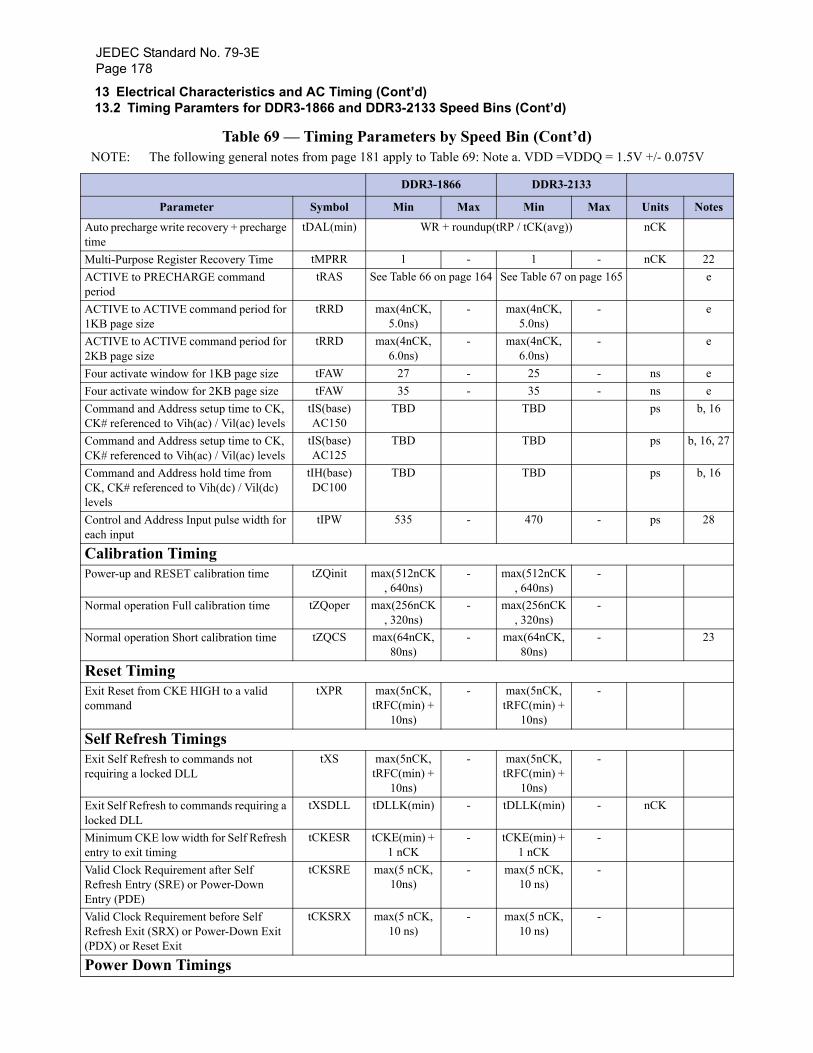
JEDEC Standard No. 79-3EPage 178
13 Electrical Characteristics and AC Timing (Cont’d)13.2 Timing Paramters for DDR3-1866 and DDR3-2133 Speed Bins (Cont’d)
Auto precharge write recovery + precharge time
tDAL(min) WR + roundup(tRP / tCK(avg)) nCK
Multi-Purpose Register Recovery Time tMPRR 1 - 1 - nCK 22ACTIVE to PRECHARGE command period
tRAS See Table 66 on page 164 See Table 67 on page 165 e
ACTIVE to ACTIVE command period for 1KB page size
tRRD max(4nCK, 5.0ns)
- max(4nCK, 5.0ns)
- e
ACTIVE to ACTIVE command period for 2KB page size
tRRD max(4nCK, 6.0ns)
- max(4nCK, 6.0ns)
- e
Four activate window for 1KB page size tFAW 27 - 25 - ns eFour activate window for 2KB page size tFAW 35 - 35 - ns eCommand and Address setup time to CK, CK# referenced to Vih(ac) / Vil(ac) levels
tIS(base) AC150
TBD TBD ps b, 16
Command and Address setup time to CK, CK# referenced to Vih(ac) / Vil(ac) levels
tIS(base) AC125
TBD TBD ps b, 16, 27
Command and Address hold time from CK, CK# referenced to Vih(dc) / Vil(dc) levels
tIH(base) DC100
TBD TBD ps b, 16
Control and Address Input pulse width for each input
tIPW 535 - 470 - ps 28
Calibration TimingPower-up and RESET calibration time tZQinit max(512nCK
, 640ns)- max(512nCK
, 640ns)-
Normal operation Full calibration time tZQoper max(256nCK, 320ns)
- max(256nCK, 320ns)
-
Normal operation Short calibration time tZQCS max(64nCK, 80ns)
- max(64nCK, 80ns)
- 23
Reset TimingExit Reset from CKE HIGH to a valid command
tXPR max(5nCK, tRFC(min) +
10ns)
- max(5nCK, tRFC(min) +
10ns)
-
Self Refresh TimingsExit Self Refresh to commands not requiring a locked DLL
tXS max(5nCK, tRFC(min) +
10ns)
- max(5nCK, tRFC(min) +
10ns)
-
Exit Self Refresh to commands requiring a locked DLL
tXSDLL tDLLK(min) - tDLLK(min) - nCK
Minimum CKE low width for Self Refresh entry to exit timing
tCKESR tCKE(min) + 1 nCK
- tCKE(min) + 1 nCK
-
Valid Clock Requirement after Self Refresh Entry (SRE) or Power-Down Entry (PDE)
tCKSRE max(5 nCK, 10ns)
- max(5 nCK, 10 ns)
-
Valid Clock Requirement before Self Refresh Exit (SRX) or Power-Down Exit (PDX) or Reset Exit
tCKSRX max(5 nCK, 10 ns)
- max(5 nCK, 10 ns)
-
Power Down Timings
Table 69 — Timing Parameters by Speed Bin (Cont’d)NOTE: The following general notes from page 181 apply to Table 69: Note a. VDD =VDDQ = 1.5V +/- 0.075V
DDR3-1866 DDR3-2133
Parameter Symbol Min Max Min Max Units Notes
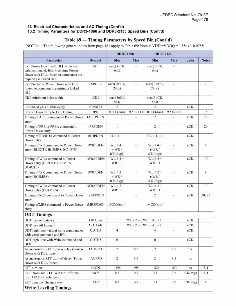
JEDEC Standard No. 79-3EPage 179
13 Electrical Characteristics and AC Timing (Cont’d)13.2 Timing Paramters for DDR3-1866 and DDR3-2133 Speed Bins (Cont’d)
Exit Power Down with DLL on to any valid command; Exit Precharge Power Down with DLL frozen to commands not requiring a locked DLL
tXP max(3nCK, 6ns)
- max(3nCK, 6ns)
-
Exit Precharge Power Down with DLL frozen to commands requiring a locked DLL
tXPDLL max(10nCK, 24ns)
- max(10nCK, 24ns)
- 2
CKE minimum pulse width tCKE max(3nCK 5ns)
- max(3nCK, 5ns)
-
Command pass disable delay tCPDED 2 - 2 - nCKPower Down Entry to Exit Timing tPD tCKE(min) 9 * tREFI tCKE(min) 9 * tREFI 15Timing of ACT command to Power Down entry
tACTPDEN 1 - 2 - nCK 20
Timing of PRE or PREA command to Power Down entry
tPRPDEN 1 - 2 - nCK 20
Timing of RD/RDA command to Power Down entry
tRDPDEN RL + 4 + 1 - RL + 4 + 1 - nCK
Timing of WR command to Power Down entry (BL8OTF, BL8MRS, BC4OTF)
tWRPDEN WL + 4 + (tWR /
tCK(avg))
- WL + 4 + (tWR /
tCK(avg))
- nCK 9
Timing of WRA command to Power Down entry (BL8OTF, BL8MRS, BC4OTF)
tWRAPDEN WL + 4 + WR + 1
- WL + 4 + WR + 1
- nCK 10
Timing of WR command to Power Down entry (BC4MRS)
tWRPDEN WL + 2 + (tWR /
tCK(avg))
- WL + 2 + (tWR /
tCK(avg))
- nCK 9
Timing of WRA command to Power Down entry (BC4MRS)
tWRAPDEN WL + 2 + WR + 1
- WL + 2 + WR + 1
- nCK 10
Timing of REF command to Power Down entry
tREFPDEN 1 - 2 - nCK 20, 21
Timing of MRS command to Power Down entry
tMRSPDEN tMOD(min) - tMOD(min) -
ODT TimingsODT turn on Latency ODTLon WL - 2 = CWL + AL - 2 nCKODT turn off Latency ODTLoff WL - 2 = CWL + AL - 2 nCKODT high time without write command or with write command and BC4
ODTH4 4 - 4 - nCK
ODT high time with Write command and BL8
ODTH8 6 - 6 - nCK
Asynchronous RTT turn-on delay (Power-Down with DLL frozen)
tAONPD 2 8.5 2 8.5 ns
Asynchronous RTT turn-off delay (Power-Down with DLL frozen)
tAOFPD 2 8.5 2 8.5 ns
RTT turn-on tAON - 195 195 - 180 180 ps 7, fRTT_Nom and RTT_WR turn-off time from ODTLoff reference
tAOF 0.3 0.7 0.3 0.7 tCK(avg) 8, f
RTT dynamic change skew tADC 0.3 0.7 0.3 0.7 tCK(avg) f
Write Leveling Timings
Table 69 — Timing Parameters by Speed Bin (Cont’d)NOTE: The following general notes from page 181 apply to Table 69: Note a. VDD =VDDQ = 1.5V +/- 0.075V
DDR3-1866 DDR3-2133
Parameter Symbol Min Max Min Max Units Notes
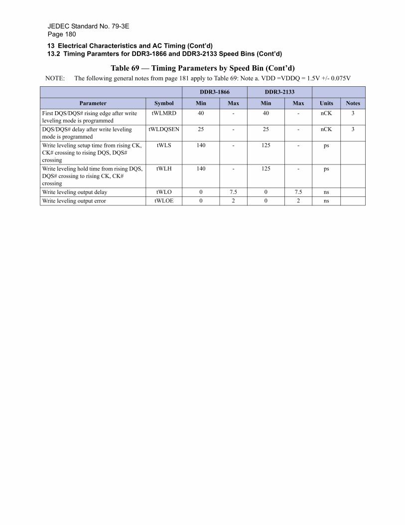
JEDEC Standard No. 79-3EPage 180
13 Electrical Characteristics and AC Timing (Cont’d)13.2 Timing Paramters for DDR3-1866 and DDR3-2133 Speed Bins (Cont’d)
First DQS/DQS# rising edge after write leveling mode is programmed
tWLMRD 40 - 40 - nCK 3
DQS/DQS# delay after write leveling mode is programmed
tWLDQSEN 25 - 25 - nCK 3
Write leveling setup time from rising CK, CK# crossing to rising DQS, DQS# crossing
tWLS 140 - 125 - ps
Write leveling hold time from rising DQS, DQS# crossing to rising CK, CK# crossing
tWLH 140 - 125 - ps
Write leveling output delay tWLO 0 7.5 0 7.5 nsWrite leveling output error tWLOE 0 2 0 2 ns
Table 69 — Timing Parameters by Speed Bin (Cont’d)NOTE: The following general notes from page 181 apply to Table 69: Note a. VDD =VDDQ = 1.5V +/- 0.075V
DDR3-1866 DDR3-2133
Parameter Symbol Min Max Min Max Units Notes
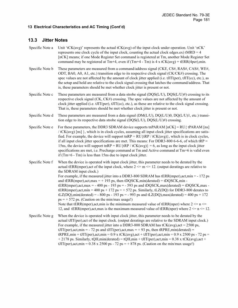
JEDEC Standard No. 79-3EPage 181
13 Electrical Characteristics and AC Timing (Cont’d)
13.3 Jitter NotesSpecific Note a Unit ‘tCK(avg)’ represents the actual tCK(avg) of the input clock under operation. Unit ‘nCK’
represents one clock cycle of the input clock, counting the actual clock edges.ex) tMRD = 4 [nCK] means; if one Mode Register Set command is registered at Tm, another Mode Register Set command may be registered at Tm+4, even if (Tm+4 - Tm) is 4 x tCK(avg) + tERR(4per),min.
Specific Note b These parameters are measured from a command/address signal (CKE, CS#, RAS#, CAS#, WE#, ODT, BA0, A0, A1, etc.) transition edge to its respective clock signal (CK/CK#) crossing. The spec values are not affected by the amount of clock jitter applied (i.e. tJIT(per), tJIT(cc), etc.), as the setup and hold are relative to the clock signal crossing that latches the command/address. That is, these parameters should be met whether clock jitter is present or not.
Specific Note c These parameters are measured from a data strobe signal (DQS(L/U), DQS(L/U)#) crossing to its respective clock signal (CK, CK#) crossing. The spec values are not affected by the amount of clock jitter applied (i.e. tJIT(per), tJIT(cc), etc.), as these are relative to the clock signal crossing. That is, these parameters should be met whether clock jitter is present or not.
Specific Note d These parameters are measured from a data signal (DM(L/U), DQ(L/U)0, DQ(L/U)1, etc.) transi-tion edge to its respective data strobe signal (DQS(L/U), DQS(L/U)#) crossing.
Specific Note e For these parameters, the DDR3 SDRAM device supports tnPARAM [nCK] = RU{ tPARAM [ns] / tCK(avg) [ns] }, which is in clock cycles, assuming all input clock jitter specifications are satis-fied. For example, the device will support tnRP = RU{tRP / tCK(avg)}, which is in clock cycles, if all input clock jitter specifications are met. This means: For DDR3-800 6-6-6, of which tRP = 15ns, the device will support tnRP = RU{tRP / tCK(avg)} = 6, as long as the input clock jitter specifications are met, i.e. Precharge command at Tm and Active command at Tm+6 is valid even if (Tm+6 - Tm) is less than 15ns due to input clock jitter.
Specific Note f When the device is operated with input clock jitter, this parameter needs to be derated by the actual tERR(mper),act of the input clock, where 2 <= m <= 12. (output deratings are relative to the SDRAM input clock.)For example, if the measured jitter into a DDR3-800 SDRAM has tERR(mper),act,min = - 172 ps and tERR(mper),act,max = + 193 ps, then tDQSCK,min(derated) = tDQSCK,min - tERR(mper),act,max = - 400 ps - 193 ps = - 593 ps and tDQSCK,max(derated) = tDQSCK,max - tERR(mper),act,min = 400 ps + 172 ps = + 572 ps. Similarly, tLZ(DQ) for DDR3-800 derates to tLZ(DQ),min(derated) = - 800 ps - 193 ps = - 993 ps and tLZ(DQ),max(derated) = 400 ps + 172 ps = + 572 ps. (Caution on the min/max usage!)Note that tERR(mper),act,min is the minimum measured value of tERR(nper) where 2 <= n <= 12, and tERR(mper),act,max is the maximum measured value of tERR(nper) where 2 <= n <= 12.
Specific Note g When the device is operated with input clock jitter, this parameter needs to be derated by the actual tJIT(per),act of the input clock. (output deratings are relative to the SDRAM input clock.)For example, if the measured jitter into a DDR3-800 SDRAM has tCK(avg),act = 2500 ps, tJIT(per),act,min = - 72 ps and tJIT(per),act,max = + 93 ps, then tRPRE,min(derated) = tRPRE,min + tJIT(per),act,min = 0.9 x tCK(avg),act + tJIT(per),act,min = 0.9 x 2500 ps - 72 ps = + 2178 ps. Similarly, tQH,min(derated) = tQH,min + tJIT(per),act,min = 0.38 x tCK(avg),act + tJIT(per),act,min = 0.38 x 2500 ps - 72 ps = + 878 ps. (Caution on the min/max usage!)
JEDEC Standard No. 79-3EPage 182
13 Electrical Characteristics and AC Timing (Cont’d)
13.4 Timing Parameter NotesNOTE 1. Actual value dependant upon measurement level definitions See Figure 45 — “Method for calcu-
lating tWPRE transitions and endpoints” on page 70 and See Figure 46 — “Method for calculat-ing tWPST transitions and endpoints” on page 70.
NOTE 2. Commands requiring a locked DLL are: READ (and RAP) and synchronous ODT commands.NOTE 3. The max values are system dependent.NOTE 4. WR as programmed in mode registerNOTE 5. Value must be rounded-up to next higher integer valueNOTE 6. There is no maximum cycle time limit besides the need to satisfy the refresh interval, tREFI.NOTE 7. For definition of RTT turn-on time tAON See 5.2.2 “Timing Parameters” on page 90.NOTE 8. For definition of RTT turn-off time tAOF See 5.2.2 “Timing Parameters” on page 90.NOTE 9. tWR is defined in ns, for calculation of tWRPDEN it is necessary to round up tWR / tCK to the
next integer.NOTE 10. WR in clock cycles as programmed in MR0.NOTE 11. The maximum read postamble is bound by tDQSCK(min) plus tQSH(min) on the left side and
tHZ(DQS)max on the right side. See Figure 28 — “Clock to Data Strobe Relationship” onpage 58
NOTE 12. Output timing deratings are relative to the SDRAM input clock. When the device is operatedwith input clock jitter, this parameter needs to be derated by t.b.d.
NOTE 13. Value is only valid for RON34NOTE 14. Single ended signal parameter. Refer to chapter <t.b.d.> for definition and measurement
method.NOTE 15. tREFI depends on TOPERNOTE 16. tIS(base) and tIH(base) values are for 1V/ns CMD/ADD single-ended slew rate and 2V/ns CK,
CK# differential slew rate. Note for DQ and DM signals, VREF(DC) = VRefDQ(DC). Forinput only pins except RESET#, VRef(DC) = VRefCA(DC). See 13.5 “Address / CommandSetup, Hold and Derating” on page 184
NOTE 17. tDS(base) and tDH(base) values are for 1V/ns DQ single-ended slew rate and 2V/ns DQS,DQS# differential slew rate. Note for DQ and DM signals, VREF(DC) = VRefDQ(DC). Forinput only pins except RESET#, VRef(DC) = VRefCA(DC). See 13.6 “Data Setup, Hold andSlew Rate Derating” on page 192.
NOTE 18. Start of internal write transaction is defined as follows:
For BL8 (fixed by MRS and on- the-fly): Rising clock edge 4 clock cycles after WL.
For BC4 (on- the- fly): Rising clock edge 4 clock cycles after WL.
For BC4 (fixed by MRS): Rising clock edge 2 clock cycles after WL.
NOTE 19. The maximum read preamble is bound by tLZ(DQS)min on the left side and tDQSCK(max) onthe right side. See Figure 28 — “Clock to Data Strobe Relationship” on page 58
NOTE 20. CKE is allowed to be registered low while operations such as row activation, precharge, auto-precharge or refresh are in progress, but power-down IDD spec will not be applied until finish-ing those operations.
NOTE 21. Although CKE is allowed to be registered LOW after a REFRESH command once tREFP-DEN(min) is satisfied, there are cases where additional time such as tXPDLL(min) is alsorequired. See 4.17.3 “Power-Down clarifications - Case 2” on page 87
JEDEC Standard No. 79-3EPage 183
13 Electrical Characteristics and AC Timing (Cont’d)13.4 Data Setup, Hold and Slew Rate Derating (Cont’d)
NOTE 22. Defined between end of MPR read burst and MRS which reloads MPR or disables MPR func-tion.
NOTE 23. One ZQCS command can effectively correct a minimum of 0.5 % (ZQ Correction) of RONand RTT impedance error within 64 nCK for all speed bins assuming the maximum sensitivi-ties specified in the ‘Output Driver Voltage and Temperature Sensitivity’ and ‘ODT Voltageand Temperature Sensitivity’ tables. The appropriate interval between ZQCS commands canbe determined from these tables and other application-specific parameters.
One method for calculating the interval between ZQCS commands, given the temperature (Tdriftrate) and voltage (Vdriftrate) drift rates that the SDRAM is subject to in the application, is illustrated. The interval could be defined by the following formula:
where TSens = max(dRTTdT, dRONdTM) and VSens = max(dRTTdV, dRONdVM) define the SDRAM temperature and voltage sensitivities.
For example, if TSens = 1.5% / oC, VSens = 0.15% / mV, Tdriftrate = 1 oC / sec and Vdriftrate = 15 mV / sec, then the interval between ZQCS commands is calculated as:
NOTE 24. n = from 13 cycles to 50 cycles. This row defines 38 parameters.NOTE 25. tCH(abs) is the absolute instantaneous clock high pulse width, as measured from one rising
edge to the following falling edge.NOTE 26. tCL(abs) is the absolute instantaneous clock low pulse width, as measured from one falling
edge to the following rising edge.NOTE 27. The tIS(base) AC150 specifications are adjusted from the tIS(base) specification by adding an
additional 100 ps of derating to accommodate for the lower alternate threshold of 150 mV andanother 25 ps to account for the earlier reference point [(175 mv - 150 mV) / 1 V/ns].
NOTE 28. Pulse width of a input signal is defined as the width between the first crossing of Vref(dc) andthe consecutive crossing of Vref(dc).
NOTE 29. tDQSL describes the instantaneous differential input low pulse width on DQS - DQS#, as mea-sured from one falling edge to the next consecutive rising edge.
NOTE 30. tDQSH describes the instantaneous differential input high pulse width on DQS - DQS#, asmeasured from one rising edge to the next consecutive falling edge.
NOTE 31. tDQSH,act + tDQSL,act = 1 tCK,act ; with tXYZ,act being the actual measured value of therespective timing parameter in the application.
NOTE 32. tDSH,act + tDSS,act = 1 tCK,act ; with tXYZ,act being the actual measured value of therespective timing parameter in the application.
ZQCorrectionTSens Tdriftrate×( ) VSens Vdriftrate×( )+
-----------------------------------------------------------------------------------------------------------------
0.51.5 1×( ) 0.15 15×( )+
------------------------------------------------------- 0.133= 128ms≈

JEDEC Standard No. 79-3EPage 184
Symb Units
tIS(base) A ps
tIS(base) A ps
tIS(base) A ps
tIS(base) A ps
tIH(base) D ps
13 Electrical Characteristics and AC Timing (Cont’d)
13.5 Address / Command Setup, Hold and DeratingFor all input signals the total tIS (setup time) and tIH (hold time) required is calculated by adding the data sheet tIS(base) and tIH(base) value (see Table 70) to the ΔtIS and ΔtIH derating value (see Table 71) respectively. Example: tIS (total setup time) = tIS(base) + ΔtIS
Setup (tIS) nominal slew rate for a rising signal is defined as the slew rate between the last crossing of VREF(dc) and the first crossing of VIH(ac)min. Setup (tIS) nominal slew rate for a falling signal is defined as the slew rate between the last crossing of VREF(dc) and the first crossing of Vil(ac)max. If the actual signal is always earlier than the nominal slew rate line between shaded ‘VREF(dc) to ac region’, use nominal slew rate for derating value (see Figure 111). If the actual signal is later than the nominal slew rate line any-where between shaded ‘VREF(dc) to ac region’, the slew rate of a tangent line to the actual signal from the ac level to VREF(dc) level is used for derating value (see Figure 113).
Hold (tIH) nominal slew rate for a rising signal is defined as the slew rate between the last crossing of Vil(dc)max and the first crossing of VREF(dc). Hold (tIH) nominal slew rate for a falling signal is defined as the slew rate between the last crossing of Vih(dc)min and the first crossing of VREF(dc). If the actual signal is always later than the nominal slew rate line between shaded ‘dc to VREF(dc) region’, use nominal slew rate for derating value (see Figure 112). If the actual signal is earlier than the nominal slew rate line any-where between shaded ‘dc to VREF(dc) region’, the slew rate of a tangent line to the actual signal from the dc level to VREF(dc) level is used for derating value (see Figure 114).
For a valid transition the input signal has to remain above/below VIH/IL(ac) for some time tVAC (see Table 75).
Although for slow slew rates the total setup time might be negative (i.e. a valid input signal will not have reached VIH/IL(ac) at the time of the rising clock transition, a valid input signal is still required to complete the transition and reach VIH/IL(ac).
For slew rates in between the values listed in Table 71, the derating values may obtained by linear interpo-lation.
These values are typically not subject to production test. They are verified by design and characterization.
Table 70 — ADD/CMD Setup and Hold Base-Values for 1V/ns
NOTE 1. (ac/dc referenced for 1V/ns Address/Command slew rate and 2 V/ns differential CK-CK# slew rate)NOTE 2. The tIS(base) AC150 specifications are adjusted from the tIS(base) AC175 specification by adding an
additional 125 ps for DDR3-800/1066 or 100ps for DDR3-1333/1600 of derating to accommodate forthe lower alternate threshold of 150 mV and another 25 ps to account for the earlier reference point[(175 mv - 150 mV) / 1 V/ns].
NOTE 3. The tIS(base) AC125 specifications are adjusted from the tIS(base) AC135 specification by adding anadditional 75 ps for DDR3-1866 and 65ps for DDR3-2133 to accommodate for the lower alternatethreshold of 125 mV and another 10 ps to account for the earlier reference point [(135 mv - 125 mV) /1 V/ns].
ol Reference DDR3-800 DDR3-1066 DDR3-1333 DDR3-1600 DDR3-1866 DDR3-2133
C175 VIH/L(ac) 200 125 65 45 - -
C150 VIH/L(ac) 350 275 190 170 - -
C135 VIH/L(ac) - - - -
C125 VIH/L(ac) - - - -
C100 VIH/L(dc) 275 200 140 120

JEDEC Standard No. 79-3EPage 185
IH
CMADSle ra V/
0
4
0
6
0
4
4
0
0
IH
CMADSle ra V/
0
4
0
6
0
4
4
0
0
13 Electrical Characteristics and AC Timing (Cont’d)13.5 Address / Command Setup, Hold and Derating (Cont’d)
Table 71 — Derating values DDR3-800/1066/1333/1600 tIS/tIH - ac/dc based AC175 Threshold
Table 72 — Derating values DDR3-800/1066/1333/1600 tIS/tIH - ac/dc based - Alternate AC150 Threshold
ΔtIS, ΔtIH derating in [ps] AC/DC basedAC175 Threshold -> VIH(ac)=VREF(dc)+175mV, VIL(ac)=VREF(dc)-175mV
CK,CK# Differential Slew Rate
4.0 V/ns 3.0 V/ns 2.0 V/ns 1.8 V/ns 1.6 V/ns 1.4 V/ns 1.2 V/ns 1.0 V/ns
ΔtIS ΔtIH ΔtIS ΔtIH ΔtIS ΔtIH ΔtIS ΔtIH ΔtIS ΔtIH ΔtIS ΔtIH ΔtIS ΔtIH ΔtIS Δt
D/Dwtens
2.0 88 50 88 50 88 50 96 58 104 66 112 74 120 84 128 10
1.5 59 34 59 34 59 34 67 42 75 50 83 58 91 68 99 8
1.0 0 0 0 0 0 0 8 8 16 16 24 24 32 34 40 5
0.9 -2 -4 -2 -4 -2 -4 6 4 14 12 22 20 30 30 38 4
0.8 -6 -10 -6 -10 -6 -10 2 -2 10 6 18 14 26 24 34 4
0.7 -11 -16 -11 -16 -11 -16 -3 -8 5 0 13 8 21 18 29 3
0.6 -17 -26 -17 -26 -17 -26 -9 -18 -1 -10 7 -2 15 8 23 2
0.5 -35 -40 -35 -40 -35 -40 -27 -32 -19 -24 -11 -16 -2 -6 5 1
0.4 -62 -60 -62 -60 -62 -60 -54 -52 -46 -44 -38 -36 -30 -26 -22 -1
ΔtIS, ΔtIH derating in [ps] AC/DC basedAlternate AC150 Threshold -> VIH(ac)=VREF(dc)+150mV, VIL(ac)=VREF(dc)-150mV
CK,CK# Differential Slew Rate
4.0 V/ns 3.0 V/ns 2.0 V/ns 1.8 V/ns 1.6 V/ns 1.4 V/ns 1.2 V/ns 1.0 V/ns
ΔtIS ΔtIH ΔtIS ΔtIH ΔtIS ΔtIH ΔtIS ΔtIH ΔtIS ΔtIH ΔtIS ΔtIH ΔtIS ΔtIH ΔtIS Δt
D/Dwtens
2.0 75 50 75 50 75 50 83 58 91 66 99 74 107 84 115 10
1.5 50 34 50 34 50 34 58 42 66 50 74 58 82 68 90 8
1.0 0 0 0 0 0 0 8 8 16 16 24 24 32 34 40 5
0.9 0 -4 0 -4 0 -4 8 4 16 12 24 20 32 30 40 4
0.8 0 -10 0 -10 0 -10 8 -2 16 6 24 14 32 24 40 4
0.7 0 -16 0 -16 0 -16 8 -8 16 0 24 8 32 18 40 3
0.6 -1 -26 -1 -26 -1 -26 7 -18 15 -10 23 -2 31 8 39 2
0.5 -10 -40 -10 -40 -10 -40 -2 -32 6 -24 14 -16 22 -6 30 1
0.4 -25 -60 -25 -60 -25 -60 -17 -52 -9 -44 -1 -36 7 -26 15 -1

JEDEC Standard No. 79-3EPage 186
IH
CMADSle ra V/
0
4
0
6
0
4
4
0
0
IH
CMADSle ra V/
0
4
0
6
0
4
4
0
0
13 Electrical Characteristics and AC Timing (Cont’d)13.5 Address / Command Setup, Hold and Derating (Cont’d)
Table 73 — Derating values DDR3-1866/2133 tIS/tIH - ac/dc based Alternate AC135 Threshold
Table 74 — Derating values DDR3-1866/2133 tIS/tIH - ac/dc based Alternate AC125 Threshold
ΔtIS, ΔtIH derating in [ps] AC/DC basedAlternate AC125 Threshold -> VIH(ac)=VREF(dc)+135mV, VIL(ac)=VREF(dc)-135mV
CK,CK# Differential Slew Rate
4.0 V/ns 3.0 V/ns 2.0 V/ns 1.8 V/ns 1.6 V/ns 1.4 V/ns 1.2 V/ns 1.0 V/ns
ΔtIS ΔtIH ΔtIS ΔtIH ΔtIS ΔtIH ΔtIS ΔtIH ΔtIS ΔtIH ΔtIS ΔtIH ΔtIS ΔtIH ΔtIS Δt
D/Dwtens
2.0 68 50 68 50 68 50 76 58 84 66 92 74 100 84 108 10
1.5 45 34 45 34 45 34 53 42 61 50 69 58 77 68 85 8
1.0 0 0 0 0 0 0 8 8 16 16 24 24 32 34 40 5
0.9 2 -4 2 -4 2 -4 10 4 18 12 26 20 34 30 42 4
0.8 3 -10 3 -10 3 -10 11 -2 19 6 27 14 35 24 43 4
0.7 6 -16 6 -16 6 -16 14 -8 22 0 30 8 38 18 46 3
0.6 9 -26 9 -26 9 -26 17 -18 25 -10 33 -2 41 8 49 2
0.5 5 -40 5 -40 5 -40 13 -32 21 -24 29 -16 37 -6 45 1
0.4 -3 -60 -3 -60 -3 -60 6 -52 14 -44 22 -36 30 -26 38 -1
ΔtIS, ΔtIH derating in [ps] AC/DC basedAlternate AC125 Threshold -> VIH(ac)=VREF(dc)+125mV, VIL(ac)=VREF(dc)-125mV
CK,CK# Differential Slew Rate
4.0 V/ns 3.0 V/ns 2.0 V/ns 1.8 V/ns 1.6 V/ns 1.4 V/ns 1.2 V/ns 1.0 V/ns
ΔtIS ΔtIH ΔtIS ΔtIH ΔtIS ΔtIH ΔtIS ΔtIH ΔtIS ΔtIH ΔtIS ΔtIH ΔtIS ΔtIH ΔtIS Δt
D/Dwtens
2.0 63 50 63 50 63 50 71 58 79 66 87 74 95 84 103 10
1.5 42 34 42 34 42 34 50 42 58 50 66 58 74 68 82 8
1.0 0 0 0 0 0 0 8 8 16 16 24 24 32 34 40 5
0.9 4 -4 4 -4 4 -4 12 4 20 12 28 20 36 30 44 4
0.8 6 -10 6 -10 6 -10 14 -2 22 6 30 14 38 24 46 4
0.7 11 -16 11 -16 11 -16 19 -8 27 0 35 8 43 18 51 3
0.6 16 -26 16 -26 16 -26 24 -18 32 -10 40 -2 48 8 56 2
0.5 15 -40 15 -40 15 -40 23 -32 31 -24 39 -16 47 -6 55 1
0.4 13 -60 13 -60 13 -60 21 -52 29 -44 37 -36 45 -26 53 -1
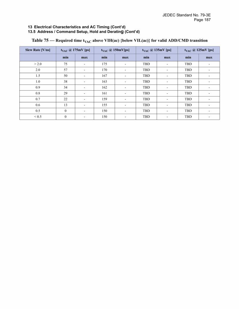
JEDEC Standard No. 79-3EPage 187
13 Electrical Characteristics and AC Timing (Cont’d)13.5 Address / Command Setup, Hold and Derating (Cont’d)
Table 75 — Required time tVAC above VIH(ac) {below VIL(ac)} for valid ADD/CMD transition
Slew Rate [V/ns] tVAC @ 175mV [ps] tVAC @ 150mV[ps] tVAC @ 135mV [ps] tVAC @ 125mV [ps]
min max min max min max min max
> 2.0 75 - 175 - TBD - TBD -
2.0 57 - 170 - TBD - TBD -
1.5 50 - 167 - TBD - TBD -
1.0 38 - 163 - TBD - TBD -
0.9 34 - 162 - TBD - TBD -
0.8 29 - 161 - TBD - TBD -
0.7 22 - 159 - TBD - TBD -
0.6 13 - 155 - TBD - TBD -
0.5 0 - 150 - TBD - TBD -
< 0.5 0 - 150 - TBD - TBD -
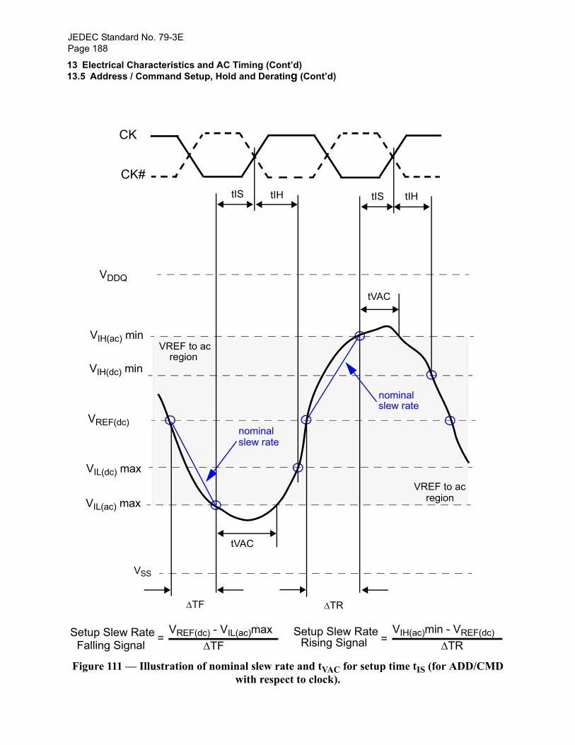
JEDEC Standard No. 79-3EPage 188
13 Electrical Characteristics and AC Timing (Cont’d)13.5 Address / Command Setup, Hold and Derating (Cont’d)
Figure 111 — Illustration of nominal slew rate and tVAC for setup time tIS (for ADD/CMD with respect to clock).
VSS
Setup Slew RateSetup Slew RateRising SignalFalling Signal
ΔTF ΔTR
VREF(dc) - VIL(ac)maxΔTF
=VIH(ac)min - VREF(dc)
ΔTR=
VDDQ
VIH(ac) min
VIH(dc) min
VREF(dc)
VIL(dc) max
VIL(ac) max
nominal
nominalslew rate
VREF to ac region
VREF to ac region
tVAC
tVAC
slew rate
CK#
CK
tIS tIH tIS tIH
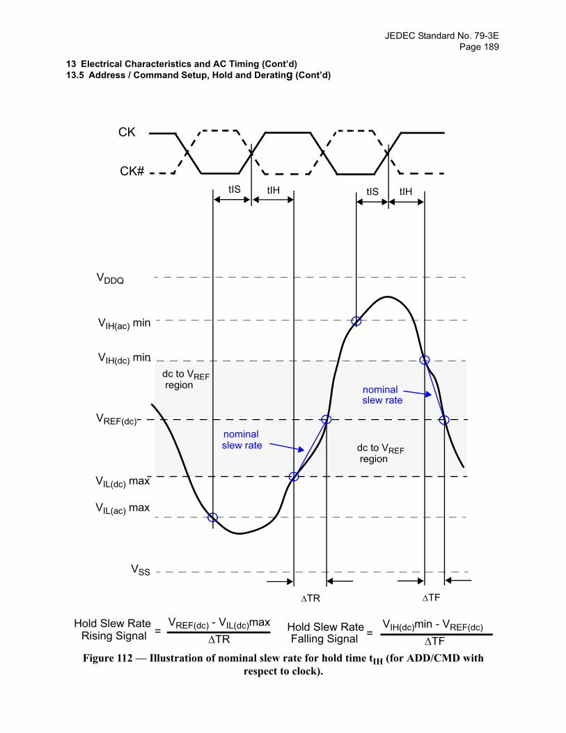
JEDEC Standard No. 79-3EPage 189
13 Electrical Characteristics and AC Timing (Cont’d)13.5 Address / Command Setup, Hold and Derating (Cont’d)
Figure 112 — Illustration of nominal slew rate for hold time tIH (for ADD/CMD with respect to clock).
VSS
Hold Slew RateHold Slew Rate Falling SignalRising Signal
ΔTR ΔTF
VREF(dc) - VIL(dc)maxΔTR
= VIH(dc)min - VREF(dc)ΔTF
=
VDDQ
VIH(ac) min
VIH(dc) min
VREF(dc)
VIL(dc) max
VIL(ac) max
nominalslew rate
nominalslew rate
dc to VREF region
dc to VREF region
CK#
CK
tIS tIH tIS tIH

JEDEC Standard No. 79-3EPage 190
13 Electrical Characteristics and AC Timing (Cont’d)13.5 Address / Command Setup, Hold and Derating (Cont’d)
Figure 113 — Illustration of tangent line for setup time tIS (for ADD/CMD with respect to clock)
VSS
Setup Slew Rate
Setup Slew Rate
Rising Signal
Falling SignalΔTF
ΔTR
tangent line[VREF(dc) - VIL(ac)max]ΔTF=
tangent line[VIH(ac)min - VREF(dc)]
ΔTR=
VDDQ
VIH(ac) min
VIH(dc) min
VREF(dc)
VIL(dc) max
VIL(ac) max
tangent
tangent
VREF to ac region
VREF to ac region
line
line
nominal line
nominal line
tVAC
tVAC
CK#
CK
tIS tIH tIS tIH
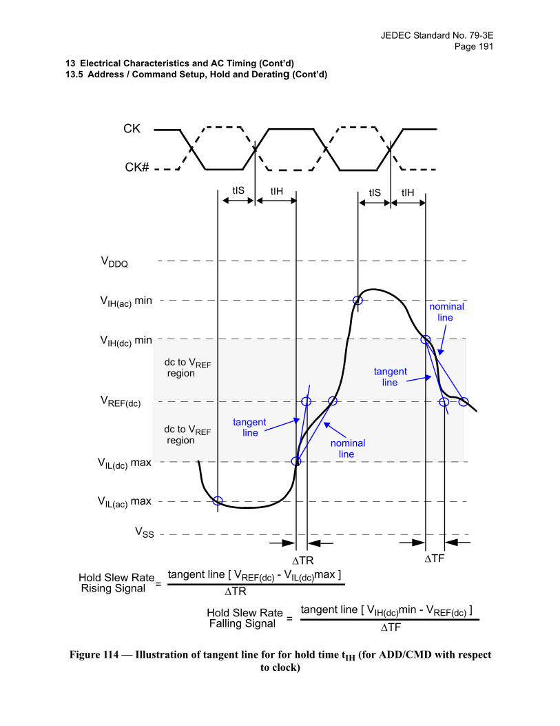
JEDEC Standard No. 79-3EPage 191
13 Electrical Characteristics and AC Timing (Cont’d)13.5 Address / Command Setup, Hold and Derating (Cont’d)
Figure 114 — Illustration of tangent line for for hold time tIH (for ADD/CMD with respect to clock)
VSS
Hold Slew Rate
ΔTFΔTR
tangent line [ VIH(dc)min - VREF(dc) ]ΔTF
=
VDDQ
VIH(ac) min
VIH(dc) min
VREF(dc)
VIL(dc) max
VIL(ac) max
tangent
tangentdc to VREF region
dc to VREF region
line
linenominal line
nominal line
Falling Signal
Hold Slew Rate tangent line [ VREF(dc) - VIL(dc)max ]ΔTR= Rising Signal
CK#
CK
tIS tIH tIS tIH
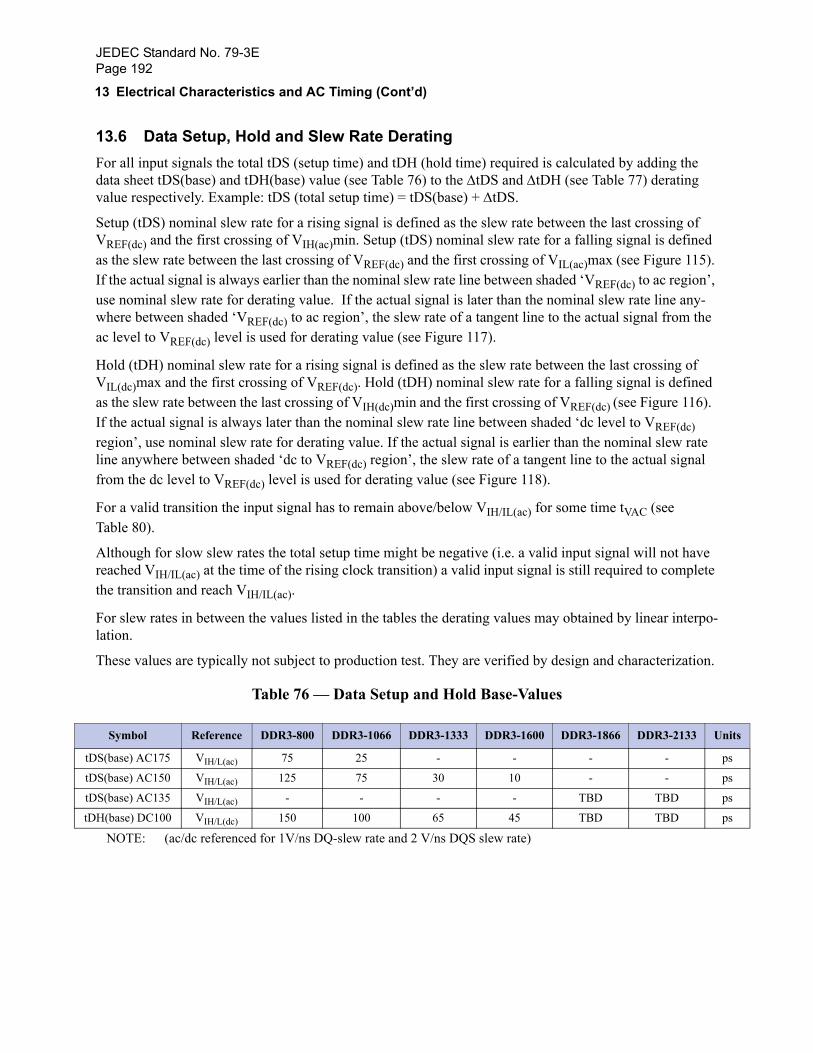
JEDEC Standard No. 79-3EPage 192
ts
13 Electrical Characteristics and AC Timing (Cont’d)
13.6 Data Setup, Hold and Slew Rate DeratingFor all input signals the total tDS (setup time) and tDH (hold time) required is calculated by adding the data sheet tDS(base) and tDH(base) value (see Table 76) to the ΔtDS and ΔtDH (see Table 77) derating value respectively. Example: tDS (total setup time) = tDS(base) + ΔtDS.
Setup (tDS) nominal slew rate for a rising signal is defined as the slew rate between the last crossing of VREF(dc) and the first crossing of VIH(ac)min. Setup (tDS) nominal slew rate for a falling signal is defined as the slew rate between the last crossing of VREF(dc) and the first crossing of VIL(ac)max (see Figure 115). If the actual signal is always earlier than the nominal slew rate line between shaded ‘VREF(dc) to ac region’, use nominal slew rate for derating value. If the actual signal is later than the nominal slew rate line any-where between shaded ‘VREF(dc) to ac region’, the slew rate of a tangent line to the actual signal from the ac level to VREF(dc) level is used for derating value (see Figure 117).
Hold (tDH) nominal slew rate for a rising signal is defined as the slew rate between the last crossing of VIL(dc)max and the first crossing of VREF(dc). Hold (tDH) nominal slew rate for a falling signal is defined as the slew rate between the last crossing of VIH(dc)min and the first crossing of VREF(dc) (see Figure 116). If the actual signal is always later than the nominal slew rate line between shaded ‘dc level to VREF(dc) region’, use nominal slew rate for derating value. If the actual signal is earlier than the nominal slew rate line anywhere between shaded ‘dc to VREF(dc) region’, the slew rate of a tangent line to the actual signal from the dc level to VREF(dc) level is used for derating value (see Figure 118).
For a valid transition the input signal has to remain above/below VIH/IL(ac) for some time tVAC (see Table 80).
Although for slow slew rates the total setup time might be negative (i.e. a valid input signal will not have reached VIH/IL(ac) at the time of the rising clock transition) a valid input signal is still required to complete the transition and reach VIH/IL(ac).
For slew rates in between the values listed in the tables the derating values may obtained by linear interpo-lation.
These values are typically not subject to production test. They are verified by design and characterization.
Table 76 — Data Setup and Hold Base-Values
NOTE: (ac/dc referenced for 1V/ns DQ-slew rate and 2 V/ns DQS slew rate)
Symbol Reference DDR3-800 DDR3-1066 DDR3-1333 DDR3-1600 DDR3-1866 DDR3-2133 Uni
tDS(base) AC175 VIH/L(ac) 75 25 - - - - ps
tDS(base) AC150 VIH/L(ac) 125 75 30 10 - - ps
tDS(base) AC135 VIH/L(ac) - - - - TBD TBD ps
tDH(base) DC100 VIH/L(dc) 150 100 65 45 TBD TBD ps
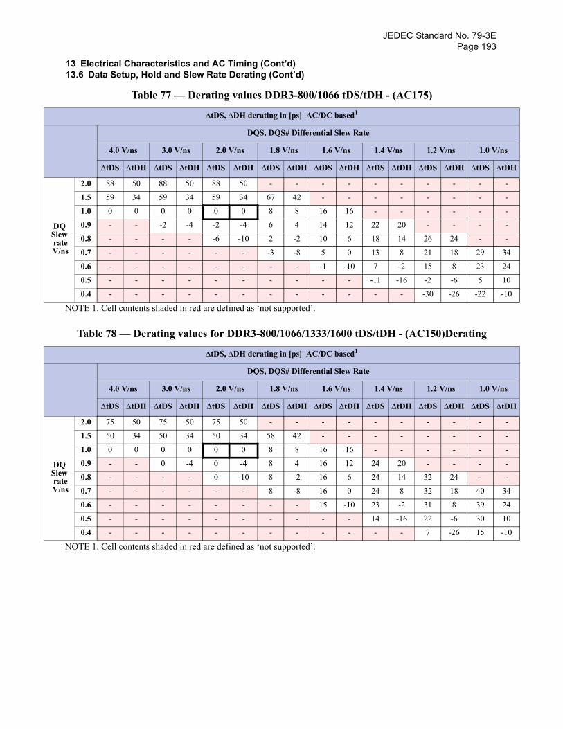
JEDEC Standard No. 79-3EPage 193
H
DSl ra V 4
4
0
0
H
DSl ra V 4
4
0
0
13 Electrical Characteristics and AC Timing (Cont’d)13.6 Data Setup, Hold and Slew Rate Derating (Cont’d)
Table 77 — Derating values DDR3-800/1066 tDS/tDH - (AC175)
Table 78 — Derating values for DDR3-800/1066/1333/1600 tDS/tDH - (AC150)Derating
ΔtDS, ΔDH derating in [ps] AC/DC based1
DQS, DQS# Differential Slew Rate
4.0 V/ns 3.0 V/ns 2.0 V/ns 1.8 V/ns 1.6 V/ns 1.4 V/ns 1.2 V/ns 1.0 V/ns
ΔtDS ΔtDH ΔtDS ΔtDH ΔtDS ΔtDH ΔtDS ΔtDH ΔtDS ΔtDH ΔtDS ΔtDH ΔtDS ΔtDH ΔtDS ΔtD
Q ewte
/ns
2.0 88 50 88 50 88 50 - - - - - - - - - -
1.5 59 34 59 34 59 34 67 42 - - - - - - - -
1.0 0 0 0 0 0 0 8 8 16 16 - - - - - -
0.9 - - -2 -4 -2 -4 6 4 14 12 22 20 - - - -
0.8 - - - - -6 -10 2 -2 10 6 18 14 26 24 - -
0.7 - - - - - - -3 -8 5 0 13 8 21 18 29 3
0.6 - - - - - - - - -1 -10 7 -2 15 8 23 2
0.5 - - - - - - - - - - -11 -16 -2 -6 5 1
0.4 - - - - - - - - - - - - -30 -26 -22 -1
NOTE 1. Cell contents shaded in red are defined as ‘not supported’.
ΔtDS, ΔDH derating in [ps] AC/DC based1
DQS, DQS# Differential Slew Rate
4.0 V/ns 3.0 V/ns 2.0 V/ns 1.8 V/ns 1.6 V/ns 1.4 V/ns 1.2 V/ns 1.0 V/ns
ΔtDS ΔtDH ΔtDS ΔtDH ΔtDS ΔtDH ΔtDS ΔtDH ΔtDS ΔtDH ΔtDS ΔtDH ΔtDS ΔtDH ΔtDS ΔtD
Q ewte
/ns
2.0 75 50 75 50 75 50 - - - - - - - - - -
1.5 50 34 50 34 50 34 58 42 - - - - - - - -
1.0 0 0 0 0 0 0 8 8 16 16 - - - - - -
0.9 - - 0 -4 0 -4 8 4 16 12 24 20 - - - -
0.8 - - - - 0 -10 8 -2 16 6 24 14 32 24 - -
0.7 - - - - - - 8 -8 16 0 24 8 32 18 40 3
0.6 - - - - - - - - 15 -10 23 -2 31 8 39 2
0.5 - - - - - - - - - - 14 -16 22 -6 30 1
0.4 - - - - - - - - - - - - 7 -26 15 -1
NOTE 1. Cell contents shaded in red are defined as ‘not supported’.
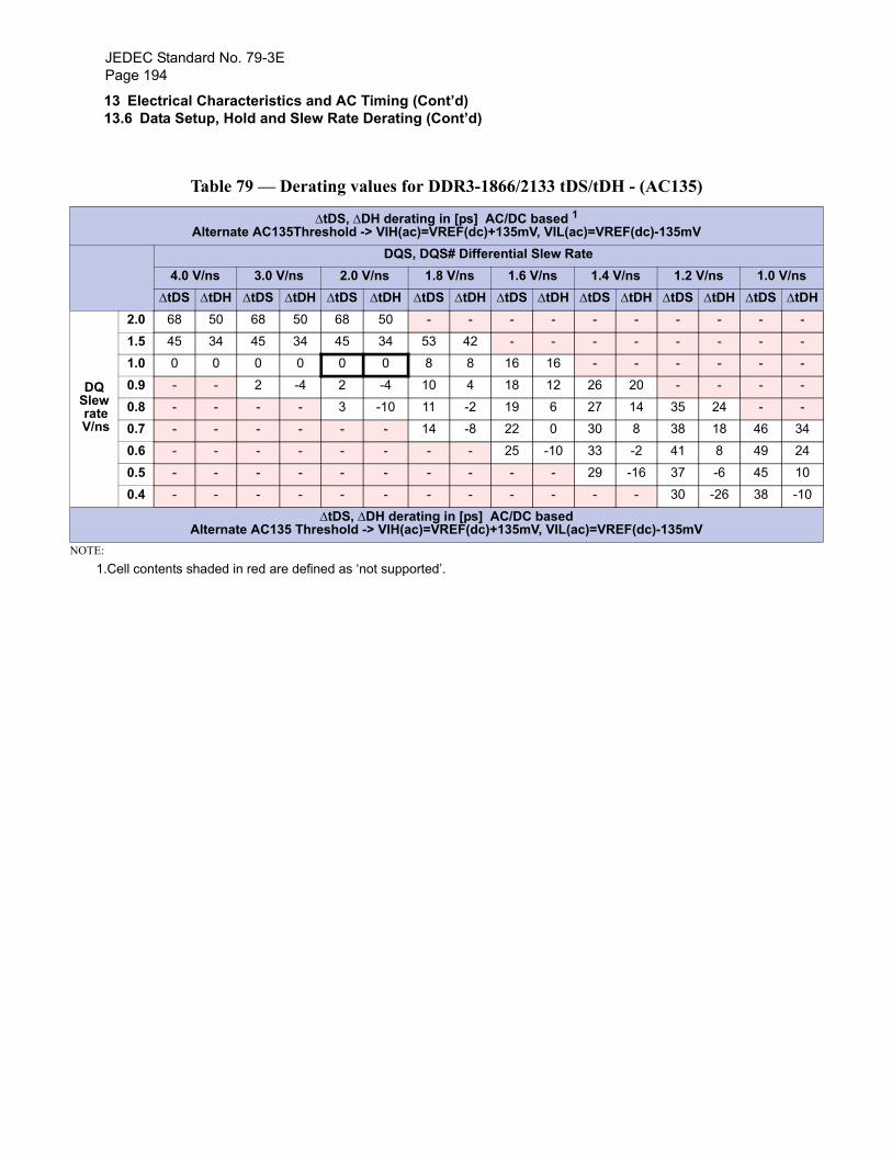
JEDEC Standard No. 79-3EPage 194
NOT
H
DSle ra V/ 4
4
0
0
13 Electrical Characteristics and AC Timing (Cont’d)13.6 Data Setup, Hold and Slew Rate Derating (Cont’d)
Table 79 — Derating values for DDR3-1866/2133 tDS/tDH - (AC135)
ΔtDS, ΔDH derating in [ps] AC/DC based 1Alternate AC135Threshold -> VIH(ac)=VREF(dc)+135mV, VIL(ac)=VREF(dc)-135mV
E:1.Cell contents shaded in red are defined as ‘not supported’.
DQS, DQS# Differential Slew Rate4.0 V/ns 3.0 V/ns 2.0 V/ns 1.8 V/ns 1.6 V/ns 1.4 V/ns 1.2 V/ns 1.0 V/ns
ΔtDS ΔtDH ΔtDS ΔtDH ΔtDS ΔtDH ΔtDS ΔtDH ΔtDS ΔtDH ΔtDS ΔtDH ΔtDS ΔtDH ΔtDS ΔtD
Q wtens
2.0 68 50 68 50 68 50 - - - - - - - - - -
1.5 45 34 45 34 45 34 53 42 - - - - - - - -
1.0 0 0 0 0 0 0 8 8 16 16 - - - - - -
0.9 - - 2 -4 2 -4 10 4 18 12 26 20 - - - -
0.8 - - - - 3 -10 11 -2 19 6 27 14 35 24 - -
0.7 - - - - - - 14 -8 22 0 30 8 38 18 46 3
0.6 - - - - - - - - 25 -10 33 -2 41 8 49 2
0.5 - - - - - - - - - - 29 -16 37 -6 45 1
0.4 - - - - - - - - - - - - 30 -26 38 -1
ΔtDS, ΔDH derating in [ps] AC/DC based Alternate AC135 Threshold -> VIH(ac)=VREF(dc)+135mV, VIL(ac)=VREF(dc)-135mV
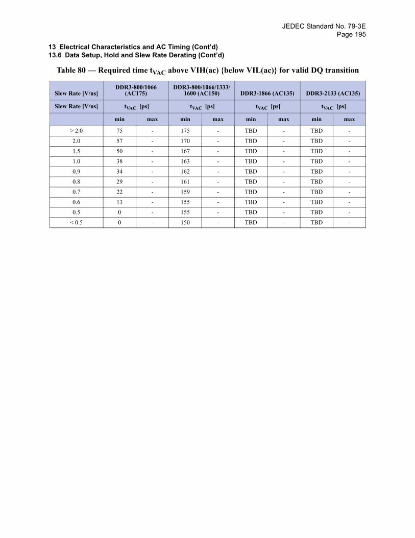
JEDEC Standard No. 79-3EPage 195
13 Electrical Characteristics and AC Timing (Cont’d)13.6 Data Setup, Hold and Slew Rate Derating (Cont’d)
Table 80 — Required time tVAC above VIH(ac) {below VIL(ac)} for valid DQ transition
Slew Rate [V/ns]DDR3-800/1066
(AC175)DDR3-800/1066/1333/
1600 (AC150) DDR3-1866 (AC135) DDR3-2133 (AC135)
Slew Rate [V/ns] tVAC [ps] tVAC [ps] tVAC [ps] tVAC [ps]
min max min max min max min max
> 2.0 75 - 175 - TBD - TBD -
2.0 57 - 170 - TBD - TBD -
1.5 50 - 167 - TBD - TBD -
1.0 38 - 163 - TBD - TBD -
0.9 34 - 162 - TBD - TBD -
0.8 29 - 161 - TBD - TBD -
0.7 22 - 159 - TBD - TBD -
0.6 13 - 155 - TBD - TBD -
0.5 0 - 155 - TBD - TBD -
< 0.5 0 - 150 - TBD - TBD -

JEDEC Standard No. 79-3EPage 196
13 Electrical Characteristics and AC Timing (Cont’d)13.6 Data Setup, Hold and Slew Rate Derating (Cont’d)
Figure 115 — Illustration of nominal slew rate and tVAC for setup time tDS (for DQ with respect to strobe)
VSS
Setup Slew RateSetup Slew RateRising SignalFalling Signal
ΔTF ΔTR
VREF(dc) - VIL(ac)maxΔTF
=VIH(ac)min - VREF(dc)
ΔTR=
VDDQ
VIH(ac) min
VIH(dc) min
VREF(dc)
VIL(dc) max
VIL(ac) max
nominal
nominalslew rate
VREF to ac region
VREF to ac region
tVAC
tVAC
slew rate
tDHtDSDQS
DQS#
tDHtDS
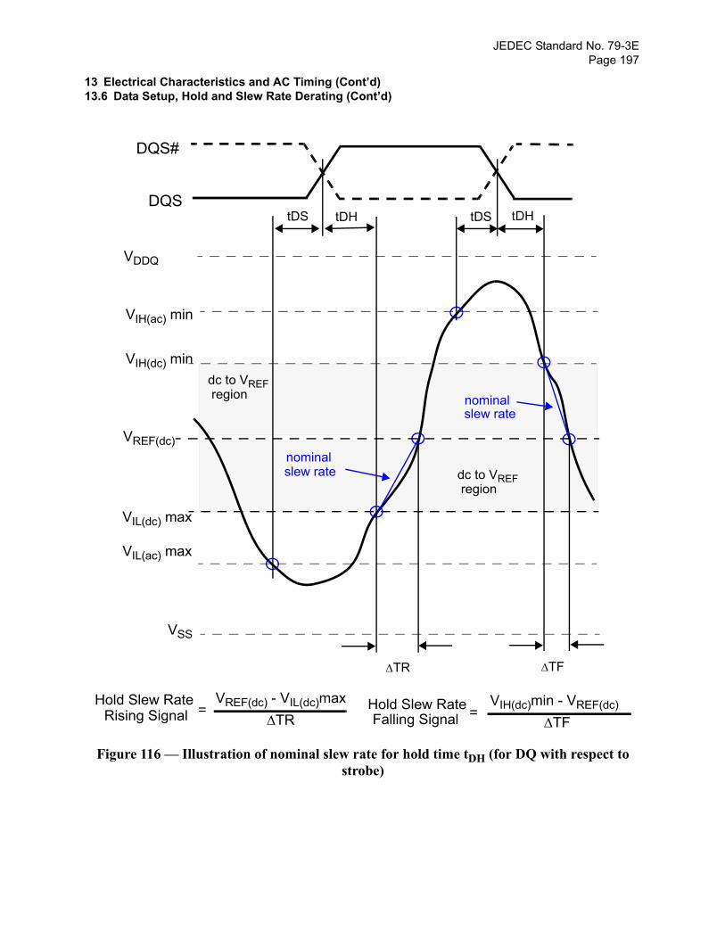
JEDEC Standard No. 79-3EPage 197
13 Electrical Characteristics and AC Timing (Cont’d)13.6 Data Setup, Hold and Slew Rate Derating (Cont’d)
Figure 116 — Illustration of nominal slew rate for hold time tDH (for DQ with respect to strobe)
VSS
Hold Slew RateHold Slew Rate Falling SignalRising Signal
ΔTR ΔTF
VREF(dc) - VIL(dc)maxΔTR
= VIH(dc)min - VREF(dc)ΔTF
=
VDDQ
VIH(ac) min
VIH(dc) min
VREF(dc)
VIL(dc) max
VIL(ac) max
nominalslew rate
nominalslew rate
dc to VREF region
dc to VREF region
tDHtDStDHtDSDQS
DQS#
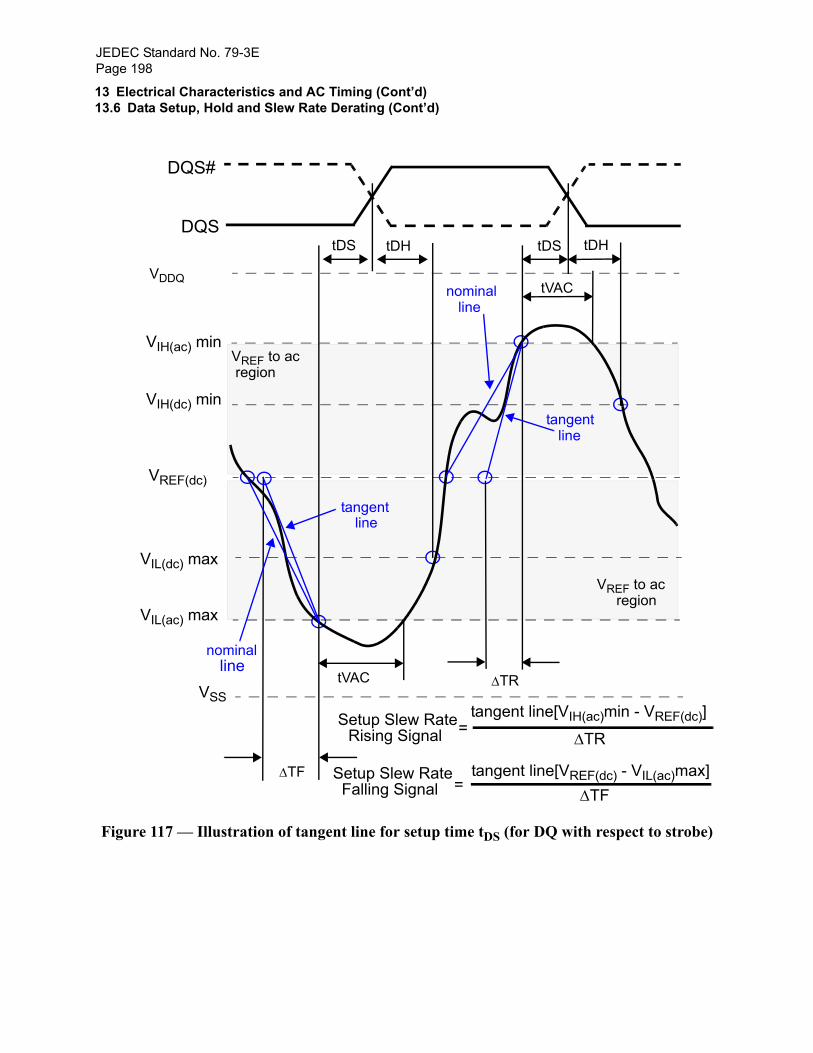
JEDEC Standard No. 79-3EPage 198
13 Electrical Characteristics and AC Timing (Cont’d)13.6 Data Setup, Hold and Slew Rate Derating (Cont’d)
Figure 117 — Illustration of tangent line for setup time tDS (for DQ with respect to strobe)
VSS
tDH
Setup Slew Rate
Setup Slew Rate
Rising Signal
Falling SignalΔTF
ΔTR
tangent line[VREF(dc) - VIL(ac)max]ΔTF=
tangent line[VIH(ac)min - VREF(dc)]
ΔTR=
VDDQ
VIH(ac) min
VIH(dc) min
VREF(dc)
VIL(dc) max
VIL(ac) max
tDS
tangent
tangent
VREF to ac region
VREF to ac region
line
line
nominal line
nominal line
tVAC
tVAC
tDHtDSDQS
DQS#
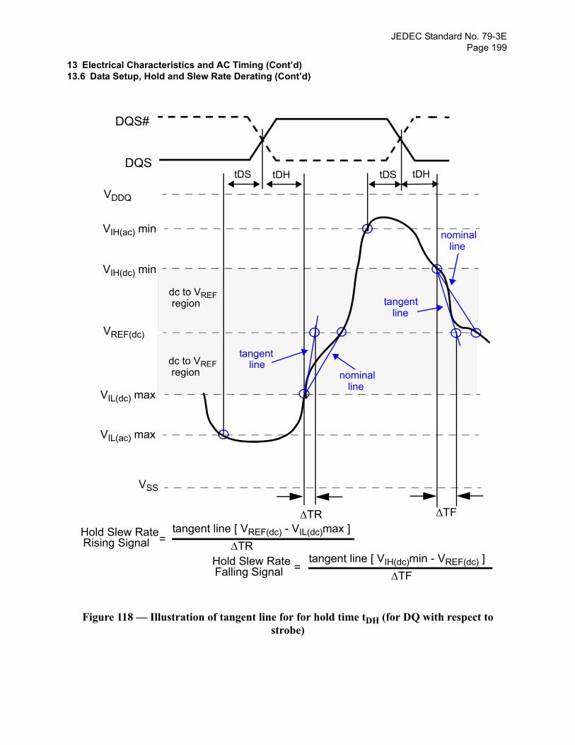
JEDEC Standard No. 79-3EPage 199
13 Electrical Characteristics and AC Timing (Cont’d)13.6 Data Setup, Hold and Slew Rate Derating (Cont’d)
Figure 118 — Illustration of tangent line for for hold time tDH (for DQ with respect to strobe)
VSS
Hold Slew Rate
ΔTFΔTR
tangent line [ VIH(dc)min - VREF(dc) ]ΔTF
=
VDDQ
VIH(ac) min
VIH(dc) min
VREF(dc)
VIL(dc) max
VIL(ac) max
tangent
tangentdc to VREF region
dc to VREF region
line
linenominal line
nominal line
Falling Signal
Hold Slew Rate tangent line [ VREF(dc) - VIL(dc)max ]ΔTR= Rising Signal
tDHtDStDHtDSDQS
DQS#

This page left blank.
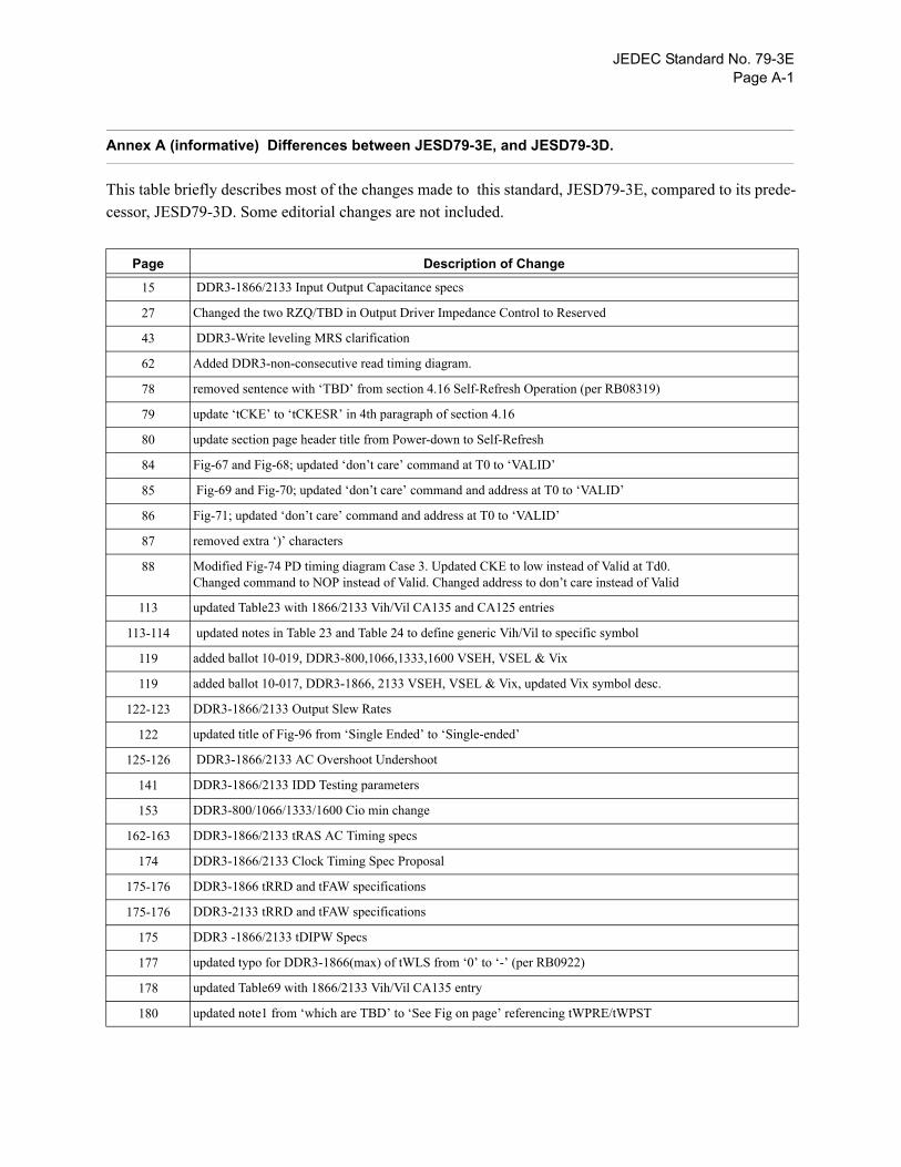
JEDEC Standard No. 79-3EPage A-1
Annex A (informative) Differences between JESD79-3E, and JESD79-3D.
This table briefly describes most of the changes made to this standard, JESD79-3E, compared to its prede-cessor, JESD79-3D. Some editorial changes are not included.
Page Description of Change
15 DDR3-1866/2133 Input Output Capacitance specs
27 Changed the two RZQ/TBD in Output Driver Impedance Control to Reserved
43 DDR3-Write leveling MRS clarification
62 Added DDR3-non-consecutive read timing diagram.
78 removed sentence with ‘TBD’ from section 4.16 Self-Refresh Operation (per RB08319)
79 update ‘tCKE’ to ‘tCKESR’ in 4th paragraph of section 4.16
80 update section page header title from Power-down to Self-Refresh
84 Fig-67 and Fig-68; updated ‘don’t care’ command at T0 to ‘VALID’
85 Fig-69 and Fig-70; updated ‘don’t care’ command and address at T0 to ‘VALID’
86 Fig-71; updated ‘don’t care’ command and address at T0 to ‘VALID’
87 removed extra ‘)’ characters
88 Modified Fig-74 PD timing diagram Case 3. Updated CKE to low instead of Valid at Td0. Changed command to NOP instead of Valid. Changed address to don’t care instead of Valid
113 updated Table23 with 1866/2133 Vih/Vil CA135 and CA125 entries
113-114 updated notes in Table 23 and Table 24 to define generic Vih/Vil to specific symbol
119 added ballot 10-019, DDR3-800,1066,1333,1600 VSEH, VSEL & Vix
119 added ballot 10-017, DDR3-1866, 2133 VSEH, VSEL & Vix, updated Vix symbol desc.
122-123 DDR3-1866/2133 Output Slew Rates
122 updated title of Fig-96 from ‘Single Ended’ to ‘Single-ended’
125-126 DDR3-1866/2133 AC Overshoot Undershoot
141 DDR3-1866/2133 IDD Testing parameters
153 DDR3-800/1066/1333/1600 Cio min change
162-163 DDR3-1866/2133 tRAS AC Timing specs
174 DDR3-1866/2133 Clock Timing Spec Proposal
175-176 DDR3-1866 tRRD and tFAW specifications
175-176 DDR3-2133 tRRD and tFAW specifications
175 DDR3 -1866/2133 tDIPW Specs
177 updated typo for DDR3-1866(max) of tWLS from ‘0’ to ‘-’ (per RB0922)
178 updated Table69 with 1866/2133 Vih/Vil CA135 entry
180 updated note1 from ‘which are TBD’ to ‘See Fig on page’ referencing tWPRE/tWPST
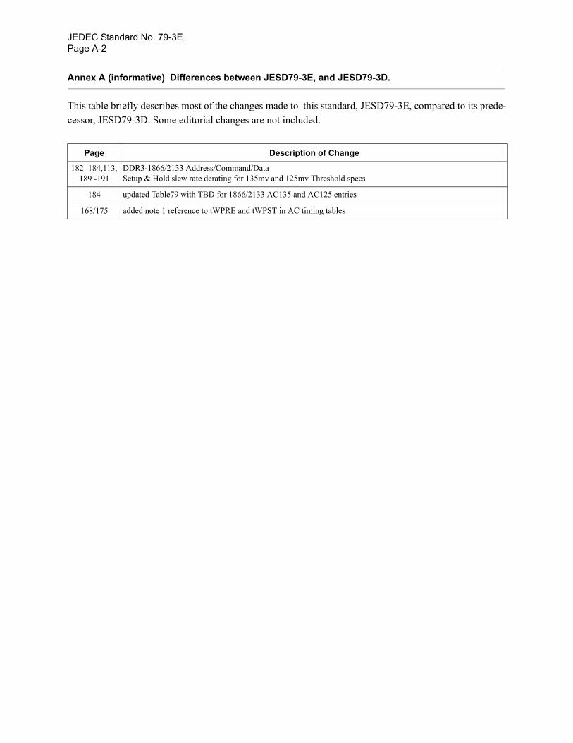
JEDEC Standard No. 79-3EPage A-2
182 -184,113, 189 -191
DDR3-1866/2133 Address/Command/Data Setup & Hold slew rate derating for 135mv and 125mv Threshold specs
184 updated Table79 with TBD for 1866/2133 AC135 and AC125 entries
168/175 added note 1 reference to tWPRE and tWPST in AC timing tables
Annex A (informative) Differences between JESD79-3E, and JESD79-3D.
This table briefly describes most of the changes made to this standard, JESD79-3E, compared to its prede-cessor, JESD79-3D. Some editorial changes are not included.
Page Description of Change
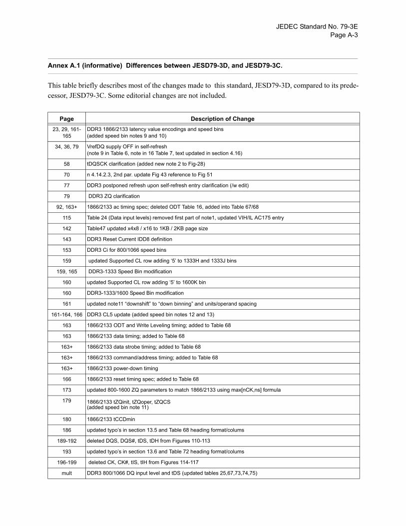
JEDEC Standard No. 79-3EPage A-3
Annex A.1 (informative) Differences between JESD79-3D, and JESD79-3C.
This table briefly describes most of the changes made to this standard, JESD79-3D, compared to its prede-cessor, JESD79-3C. Some editorial changes are not included.
Page Description of Change23, 29, 161-
165DDR3 1866/2133 latency value encodings and speed bins(added speed bin notes 9 and 10)
34, 36, 79 VrefDQ supply OFF in self-refresh (note 9 in Table 6, note in 16 Table 7, text updated in section 4.16)
58 tDQSCK clarification (added new note 2 to Fig-28)
70 n 4.14.2.3, 2nd par. update Fig 43 reference to Fig 51
77 DDR3 postponed refresh upon self-refresh entry clarification (/w edit)
79 DDR3 ZQ clarification
92, 163+ 1866/2133 ac timing spec; deleted ODT Table 16, added into Table 67/68
115 Table 24 (Data input levels) removed first part of note1, updated VIH/IL AC175 entry
142 Table47 updated x4x8 / x16 to 1KB / 2KB page size
143 DDR3 Reset Current IDD8 definition
153 DDR3 Ci for 800/1066 speed bins
159 updated Supported CL row adding ‘5’ to 1333H and 1333J bins
159, 165 DDR3-1333 Speed Bin modification
160 updated Supported CL row adding ‘5’ to 1600K bin
160 DDR3-1333/1600 Speed Bin modification
161 updated note11 “downshift” to “down binning” and units/operand spacing
161-164, 166 DDR3 CL5 update (added speed bin notes 12 and 13)
163 1866/2133 ODT and Write Leveling timing; added to Table 68
163 1866/2133 data timing; added to Table 68
163+ 1866/2133 data strobe timing; added to Table 68
163+ 1866/2133 command/address timing; added to Table 68
163+ 1866/2133 power-down timing
166 1866/2133 reset timing spec; added to Table 68
173 updated 800-1600 ZQ parameters to match 1866/2133 using max[nCK,ns] formula
179 1866/2133 tZQinit, tZQoper, tZQCS(added speed bin note 11)
180 1866/2133 tCCDmin
186 updated typo’s in section 13.5 and Table 68 heading format/colums
189-192 deleted DQS, DQS#, tDS, tDH from Figures 110-113
193 updated typo’s in section 13.6 and Table 72 heading format/colums
196-199 deleted CK, CK#, tIS, tIH from Figures 114-117
mult DDR3 800/1066 DQ input level and tDS (updated tables 25,67,73,74,75)
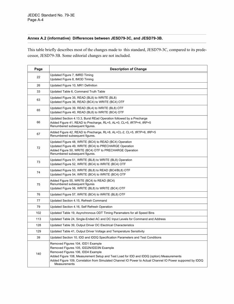
JEDEC Standard No. 79-3EPage A-4
Annex A.2 (informative) Differences between JESD79-3C, and JESD79-3B.
This table briefly describes most of the changes made to this standard, JESD79-3C, compared to its prede-cessor, JESD79-3B. Some editorial changes are not included.
Page Description of Change
22Updated Figure 7, tMRD TimingUpdated Figure 8, tMOD Timing
26 Updated Figure 10, MR1 Definition
33 Updated Table 6, Command Truth Table
63Updated Figure 35, READ (BL8) to WRITE (BL8)Updated Figure 36, READ (BC4) to WRITE (BC4) OTF
65Updated Figure 39, READ (BL4) to WRITE (BL8) OTFUpdated Figure 40, READ (BL8) to WRITE (BC4) OTF
66Updated Section 4.13.3, Burst REad Operation followed by a PrechargeAdded Figure 41, READ to Precharge, RL=5, AL=0, CL=5, tRTP=4, tRP=5Renumbered subsequent figures.
67 Added Figure 42, READ to Precharge, RL=8, AL=CL-2, CL=5, tRTP=6, tRP=5Renumbered subsequent figures.
72
Updated Figure 48, WRITE (BC4) to READ (BC4) OperationUpdated Figure 49, WRITE (BC4) to PRECHARGE OperationAdded Figure 50, WRITE (BC4) OTF to PRECHARGE OperationRenumbered subsequent figures.
73Updated Figure 51, WRITE (BL8) to WRITE (BL8) OperationUpdated Figure 52, WRITE (BC4) to WRITE (BC4) OTF
74Updated Figure 53, WRITE (BL8) to READ (BC4/BL8) OTFUpdated Figure 54, WRITE (BC4) to WRITE (BC4) OTF
75Added Figure 55, WRITE (BC4) to READ (BC4) Renumbered subsequent figuresUpdated Figure 56, WRITE (BL8) to WRITE (BC4) OTF
76 Updated Figure 57, WRITE (BC4) to WRITE (BL8) OTF
77 Updated Section 4.15, Refresh Command
79 Updated Section 4.16, Self Refresh Operation
102 Updated Table 19, Asynchronous ODT Timing Paramaters for all Speed Bins
113 Updated Table 24, Single-Ended AC and DC Input Levels for Command and Address
128 Updated Table 39, Output Driver DC Electrical Characteristics
129 Updated Table 41, Output Driver Voltage and Temperature Sensitivity
39 Updated Section 10, IDD and IDDQ Specification Parameters and Test Conditions
140
Removed Figures 104, IDD1 ExampleRemoved Figures 105, IDD2N/IDD3N ExampleRemoved Figures 106, IDD4 ExampleAdded Figure 108, Measurement Setup and Test Load for IDD and IDDQ (option) MeasurementsAdded Figure 109, Correlation from Simulated Channel IO Power to Actual Channel IO Power suppored by IDDQ
Measurements
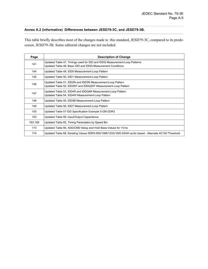
JEDEC Standard No. 79-3EPage A-5
141Updated Table 47, Timings used for IDD and IDDQ Measurement-Loop PatternsUpdated Table 48, Basic IDD and IDDQ Measurement Conditions
144 Updated Table 49, IDD0 Measurement-Loop Pattern
145 Updated Table 50, IDD1 Measurement-Loop Pattern
146Updated Table 51, IDD2N and IDD3N Measurement-Loop PatternUpdated Table 52, IDD2NT and IDDQ2NT Measurement-Loop Pattern
147Updated Table 53, IDD4R and IDDQ4R Measurement-Loop PatternUpdated Table 54, IDD4W Measurement-Loop Pattern
148 Updated Table 55, IDD5B Measurement-Loop Pattern
149 Updated Table 56, IDD7 Measurement-Loop Pattern
150 Updated Table 57 IDD Specification Example 512M DDR3
153 Updated Table 59, Input/Output Capacitance
163-169 Updated Table 65, Timing Paramaters by Speed Bin
173 Updated Table 66, ADD/CMD Setup and Hold Base-Values for 1V/ns
174 Updated Table 68, Derating Values DDR3-800/1066/1333/1600 tIS/tIH ac/dc based - Alternate AC150 Threshold
Annex A.2 (informative) Differences between JESD79-3C, and JESD79-3B.
This table briefly describes most of the changes made to this standard, JESD79-3C, compared to its prede-cessor, JESD79-3B. Some editorial changes are not included.
Page Description of Change
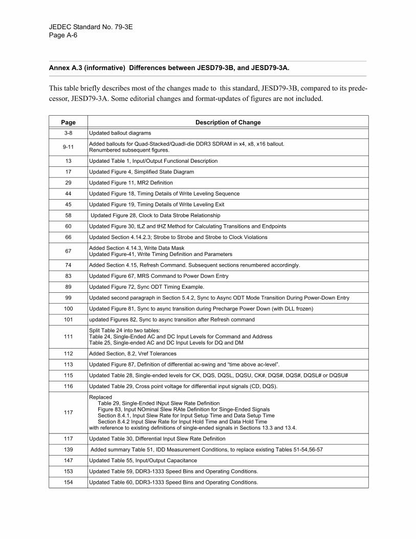
JEDEC Standard No. 79-3EPage A-6
Annex A.3 (informative) Differences between JESD79-3B, and JESD79-3A.
This table briefly describes most of the changes made to this standard, JESD79-3B, compared to its prede-cessor, JESD79-3A. Some editorial changes and format-updates of figures are not included.
Page Description of Change3-8 Updated ballout diagrams
9-11 Added ballouts for Quad-Stacked/Quadl-die DDR3 SDRAM in x4, x8, x16 ballout.Renumbered subsequent figures.
13 Updated Table 1, Input/Output Functional Description
17 Updated Figure 4, Simplified State Diagram
29 Updated Figure 11, MR2 Definition
44 Updated Figure 18, Timing Details of Write Leveling Sequence
45 Updated Figure 19, Timing Details of Write Leveling Exit
58 Updated Figure 28, Clock to Data Strobe Relationship
60 Updated Figure 30, tLZ and tHZ Method for Calculating Transitions and Endpoints
66 Updated Section 4.14.2.3; Strobe to Strobe and Strobe to Clock Violations
67 Added Section 4.14.3, Write Data MaskUpdated Figure-41, Write Timing Definition and Parameters
74 Added Section 4.15, Refresh Command. Subsequent sections renumbered accordingly.
83 Updated Figure 67, MRS Command to Power Down Entry
89 Updated Figure 72, Sync ODT Timing Example.
99 Updated second paragraph in Section 5.4.2, Sync to Async ODT Mode Transition During Power-Down Entry
100 Updated Figure 81, Sync to async transition during Precharge Power Down (with DLL frozen)
101 updated Figures 82, Sync to async transition after Refresh command
111Split Table 24 into two tables:Table 24, Single-Ended AC and DC Input Levels for Command and AddressTable 25, Single-ended AC and DC Input Levels for DQ and DM
112 Added Section, 8.2, Vref Tolerances
113 Updated Figure 87, Definition of differential ac-swing and “time above ac-level”.
115 Updated Table 28, Single-ended levels for CK, DQS, DQSL, DQSU, CK#, DQS#, DQS#, DQSL# or DQSU#
116 Updated Table 29, Cross point voltage for differential input signals (CD, DQS).
117
Replaced Table 29, Single-Ended INput Slew Rate DefinitionFigure 83, Input NOminal Slew RAte Definition for Singe-Ended SignalsSection 8.4.1, Input Slew Rate for Input Setup Time and Data Setup TimeSection 8.4.2 Input Slew Rate for Input Hold Time and Data Hold Time
with reference to existing definitions of single-ended signals in Sections 13.3 and 13.4.
117 Updated Table 30, Differential Input Slew Rate Definition
139 Added summary Table 51, IDD Measurement Conditions, to replace existing Tables 51-54,56-57
147 Updated Table 55, Input/Output Capacitance
153 Updated Table 59, DDR3-1333 Speed Bins and Operating Conditions.
154 Updated Table 60, DDR3-1333 Speed Bins and Operating Conditions.
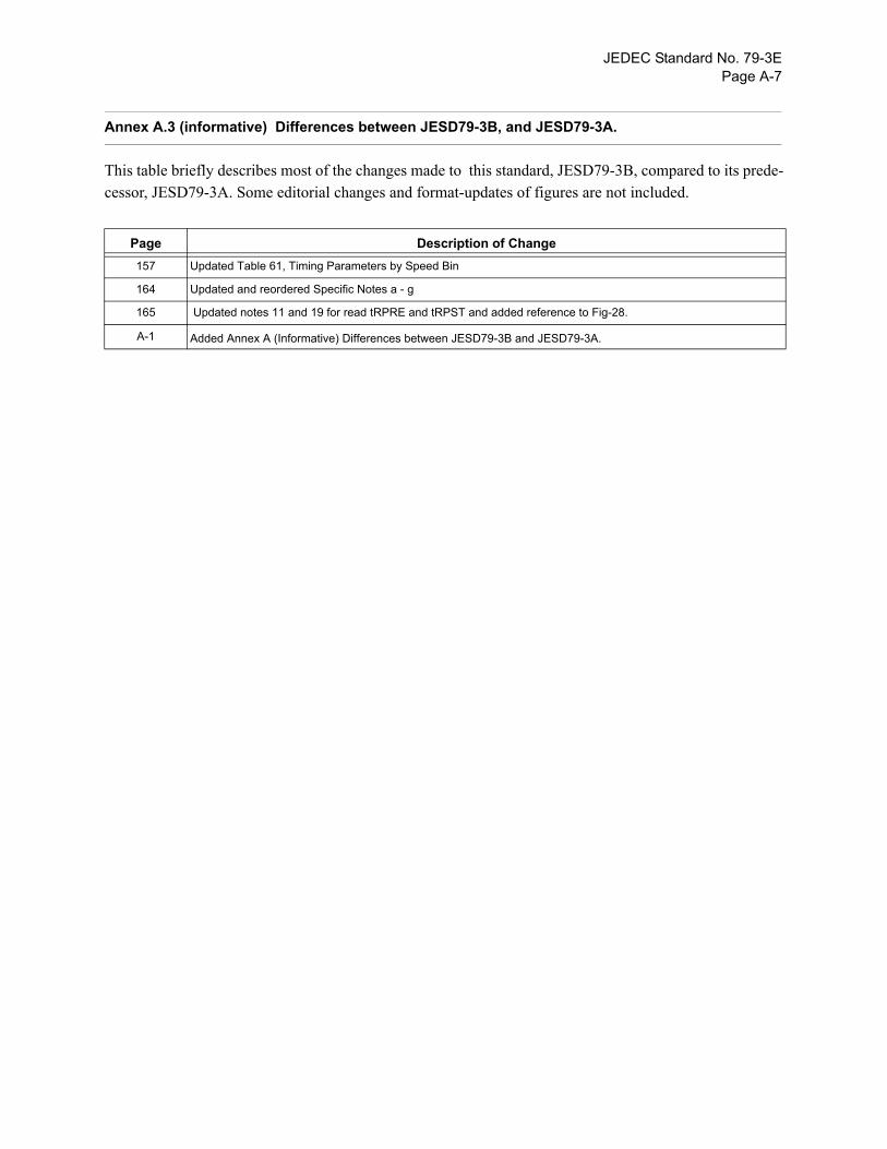
JEDEC Standard No. 79-3EPage A-7
157 Updated Table 61, Timing Parameters by Speed Bin
164 Updated and reordered Specific Notes a - g
165 Updated notes 11 and 19 for read tRPRE and tRPST and added reference to Fig-28.
A-1 Added Annex A (Informative) Differences between JESD79-3B and JESD79-3A.
Annex A.3 (informative) Differences between JESD79-3B, and JESD79-3A.
This table briefly describes most of the changes made to this standard, JESD79-3B, compared to its prede-cessor, JESD79-3A. Some editorial changes and format-updates of figures are not included.
Page Description of Change
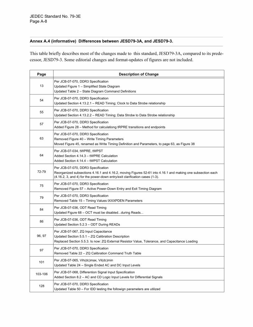
JEDEC Standard No. 79-3EPage A-8
Annex A.4 (informative) Differences between JESD79-3A, and JESD79-3.
This table briefly describes most of the changes made to this standard, JESD79-3A, compared to its prede-cessor, JESD79-3. Some editorial changes and format-updates of figures are not included.
Page Description of Change
13Per JCB-07-070, DDR3 SpecificationUpdated Figure 1 – Simplified State DiagramUpdated Table 2 – State Diagram Command Definitions
54 Per JCB-07-070, DDR3 SpecificationUpdated Section 4.13.2.1 – READ Timing; Clock to Data Strobe relationship
55 Per JCB-07-070, DDR3 SpecificationUpdated Section 4.13.2.2 – READ Timing; Data Strobe to Data Strobe relationship
57 Per JCB-07-070, DDR3 SpecificationAdded Figure 28 – Method for calculationg tRPRE transitions and endpoints
63Per JCB-07-070, DDR3 SpecificationRemoved Figure 40 – Write Timing ParametersMoved Figure 45, renamed as Write Timing Definition and Parameters, to page 63, as Figure 38
64Per JCB-07-034, tWPRE, tWPSTAdded Section 4.14.3 – tWPRE CalculationAdded Section 4.14.4 – tWPST Calculation
72-79Per JCB-07-070, DDR3 SpecificationReorganized subsections 4.16.1 and 4.16.2, moving Figures 52-61 into 4.16.1 and making one subsection each (4.16.2, 3, and 4) for the power-down entry/exit clarification cases (1-3).
75 Per JCB-07-070, DDR3 SpecificationRemoved Figure 57 – Active Power-Down Entry and Exit Timing Diagram
79 Per JCB-07-070, DDR3 SpecificationRemoved Table 15 – Timing Values tXXXPDEN Parameters
84 Per JCB-07-036, ODT Read TimingUpdated Figure 68 – OCT must be disabled...during Reads...
86 Per JCB-07-036, ODT Read TimingUpdated Section 5.2.3 – ODT During READs
96, 97Per JCB-07-067, ZQ Input CapacitanceUpdated Section 5.5.1 – ZQ Calibration DescriptionReplaced Section 5.5.3. Is now: ZQ External Resistor Value, Tolerance, and Capacitance Loading
97 Per JCB-07-070, DDR3 SpecificationRemoved Table 22 – ZQ Calibration Command Truth Table
101 Per JCB-07-065, Vih(dc)max, Vil(dc)minUpdated Table 24 – Single Ended AC and DC Input Levels
103-106 Per JCB-07-068, Differention Signal Input SpecificationAdded Section 8.2 – AC and CD Logic Input Levels for Differential Signals
128 Per JCB-07-070, DDR3 SpecificationUpdated Table 50 – For IDD testing the followign parameters are utilized

JEDEC Standard No. 79-3EPage A-9
141 Per JCB-07-038, CapacitanceUpdated Table 61 – Input/Output Capacitance
141 Per JCB-07-067, ZQ Input CapacitanceUpdated Table 61 – Input/Output Capacitance
142, 143Per JCB-07-070, DDR3 SpecificationRemoved unnumbered tables from subsection 12.1. Moved subsection 12.2 material into 12.1. Renumbered subse-quent subsections.
149 Per JCB-07-041, tJIT (duty) note modificationUpdated Table 67 – Timing Parameters by Speed Bin
149, 150 Per JCB-07-032, Cumulative JitterUpdated Table 67 – Timing Parameters by Speed Bin
150 Per JCB-07-034, tWPRE, tWPSTUpdated Table 67 – Timing Parameters by Speed Bin
150 Per JCB-07-040, Jitter Values for DDR3-1600Updated Table 67 – Timing Parameters by Speed Bin
150 Per JCB-07-029, Jitter Output Derating Updated Table 67 – Timing Parameters by Speed Bin
150 Per JCB-07-031, tDQSCK tQHUpdated Table 67 – Timing Parameters by Speed Bin
150 Per JCB-07-066, tQSH, tQSL valuesUpdated Table 67 – Timing Parameters by Speed Bin
152 Per JCB-07-042, tIS, tIH, DDR3-1333Updated Table 67 – Timing Parameters by Speed Bin
154 Per JCB-07-035, tWLS, tWLHUpdated Table 67 – Timing Parameters by Speed Bin
156-158
Per JCB-07-033, tCH (abs) and tCL (abs)Removed Specific Note F from Table 67 – Timing Parameters by Speed Bin. This action included remvoing
the Table – Min and Max SPEC values.Removed Note 22 from Table 67 – Timing Parameters by Speed BinAdded Notes 25 and 26 to Table 67 – Timing Parameters by Speed Bin
157 Per JCB-07-039, tZQCSAdded Note 23
157, 158 Per JCB-07-039, tZQCSUpdated Note 23 of Table 67 – Timing Parameters by Speed Bin
158 Per JCB-07-042, tIS, tIH, DDR3-1333Added Note 27
159 Per JCB-07-027Updated Table 68 – ADD/CMD Setup and Hold Base-Values for 1V/ns
Annex A.4 (informative) Differences between JESD79-3A, and JESD79-3.
This table briefly describes most of the changes made to this standard, JESD79-3A, compared to its prede-cessor, JESD79-3. Some editorial changes and format-updates of figures are not included.
Page Description of Change
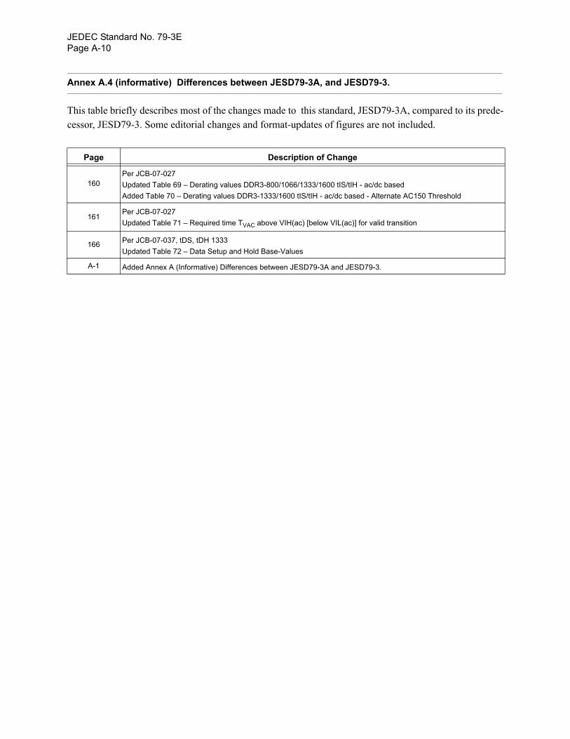
JEDEC Standard No. 79-3EPage A-10
160Per JCB-07-027Updated Table 69 – Derating values DDR3-800/1066/1333/1600 tIS/tIH - ac/dc basedAdded Table 70 – Derating values DDR3-1333/1600 tIS/tIH - ac/dc based - Alternate AC150 Threshold
161Per JCB-07-027Updated Table 71 – Required time TVAC above VIH(ac) [below VIL(ac)] for valid transition
166 Per JCB-07-037, tDS, tDH 1333Updated Table 72 – Data Setup and Hold Base-Values
A-1 Added Annex A (Informative) Differences between JESD79-3A and JESD79-3.
Annex A.4 (informative) Differences between JESD79-3A, and JESD79-3.
This table briefly describes most of the changes made to this standard, JESD79-3A, compared to its prede-cessor, JESD79-3. Some editorial changes and format-updates of figures are not included.
Page Description of Change

Rev. 9/02
Standard Improvement Form JEDEC JESD79-3E The purpose of this form is to provide the Technical Committees of JEDEC with input from the industry regarding usage of the subject standard. Individuals or companies are invited to submit comments to JEDEC. All comments will be collected and dispersed to the appropriate committee(s). If you can provide input, please complete this form and return to:
JEDEC Attn: Publications Department 3103 North 10th Street Suite 240 South Arlington, VA 22201-2107
Fax: 703.907.7583
1. I recommend changes to the following: Requirement, clause number
Test method number Clause number The referenced clause number has proven to be: Unclear Too Rigid In Error
Other
2. Recommendations for correction:
3. Other suggestions for document improvement:
Submitted by
Name: Phone:
Company: E-mail:
Address:
City/State/Zip: Date:


![4Gb Q-die DDR3 SDRAM - Samsung · Table Of Contents 4Gb Q-die DDR3 SDRAM 1. ... DDR3 SDRAM Addressing ... [ Table 1 ] Samsung 4Gb DDR3 Q-die ordering information table](https://static.documents.pub/doc/80x56/5ad5dbf67f8b9a5c638d9a46/4gb-q-die-ddr3-sdram-of-contents-4gb-q-die-ddr3-sdram-1-ddr3-sdram-addressing.jpg)


