The line width (minimum design dimension) for semiconductor circuits which reached the sub-micron (1 μm = one-millionth of a meter) range in the 1980s has in recent years entered the nanometer realm (1-nm = one-billionth of a meter) with line widths of 65 nm or 45 nm. Meanwhile, further research and development is in progress around the world aimed at improving process miniaturization to achieve line widths of 32 nm, 22 nm, or less. The CD-SEM is an essential tool for performing measurements in conjunction with this next-generation nano-scale processing. Hitachi High-Technologies Corporation, which has an international market share exceeding 80%, has been supplying its latest CD-SEMs to imec, a Belgian-based international research institute, since 2005 and is working with imec on joint research into measurement systems with an eye to the sub-10-nm era of processing technology. Lithography Research Undertaken through International Consortium Imec (Interuniversity Microelectronics Center) is an independent research institute based in Belgium that, since its establishment in 1984, has been conducting basic research in the fields of microelectronics and nanotechnology with a focus on the needs of industry 3 to 10 years into the future. The research is conducted on an open innovation basis with participation by world-leading companies in the IT (information technology), device, production machinery, materials, and other sectors. At the Imec Executive Seminar 2010 held in Tokyo during November 2010, imec President & Chief Executive Officer, Luc Van den hove, presented an image of society in the near future and described the many different fields in which imec is involved. Research leaders presented the latest results from their respective fields including energy systems, healthcare solutions, smart systems (information and telecommunications systems), and next-generation devices. One presentation of particular interest was given by Kurt Ronse, Director of the Advanced Lithography Program, on the subject of EUV (extreme ultraviolet) lithography. Joint Research with imec Belgium Targeting Measurement for 10-nm Generation Special Report Corporations from around the world collaborate at imec on basic research into microelectronics and nanotechnology. 173
Transcript
The line width (minimum design dimension) for semiconductor circuits which reached the sub-micron (1 μm = one-millionth of a meter) range in the 1980s has in recent years entered the nanometer realm (1-nm = one-billionth of a meter) with line widths of 65 nm or 45 nm. Meanwhile, further research and development is in progress around the world aimed at improving process miniaturization to achieve line widths of 32 nm, 22 nm, or less. The CD-SEM is an essential tool for performing measurements in conjunction with this next-generation nano-scale processing. Hitachi High-Technologies Corporation, which has an international market share exceeding 80%, has been supplying its latest CD-SEMs to imec, a Belgian-based international research institute, since 2005 and is working with imec on joint research into measurement systems with an eye to the sub-10-nm era of processing technology.
Lithography Research Undertaken through International ConsortiumImec (Interuniversity Microelectronics Center) is an independent research institute based in Belgium that, since its establishment in 1984, has been conducting basic r e s e a r c h i n t h e f i e l d s o f m i c r o e l e c t r o n i c s a n d nanotechnology with a focus on the needs of industry 3 to 10 years into the future. The research is conducted on an open innovation basis with participation by world-leading companies in the IT (information technology), device, production machinery, materials, and other sectors.
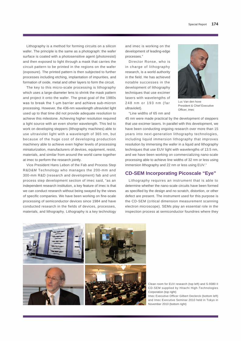
At the Imec Executive Seminar 2010 held in Tokyo during November 2010, imec President & Chief Executive Officer, Luc Van den hove, presented an image of society in the near future and described the many different fields in which imec is involved. Research leaders presented the latest results from their respective fields including energy systems, healthcare solutions, smart systems (information and telecommunications systems), and next-generation devices.
One presentation of particular interest was given by Kurt Ronse, Director of the Advanced Lithography Program, on the subject of EUV (extreme ultraviolet) lithography.
Joint Research with imec Belgium Targeting Measurement for 10-nm Generation
Special Report
Corporations from around the world collaborate at imec on basic research into microelectronics and nanotechnology.
173
CD-SEM Incorporating Picoscale “Eye”
Lithography is a method for forming circuits on a silicon wafer. The principle is the same as a photograph: the wafer surface is coated with a photosensitive agent (photoresist) and then exposed to light through a mask that carries the circuit pattern to be printed in the regions on the wafer (exposure). The printed pattern is then subjected to further processes including etching, implantation of impurities, and formation of oxide, metal and other layers to form the circuit.
The key to this micro-scale processing is lithography which uses a large-diameter lens to shrink the mask pattern and project it onto the wafer. The great goal of the 1980s was to break the 1-μm barrier and achieve sub-micron processing. However, the 436-nm wavelength ultraviolet light used up to that time did not provide adequate resolution to achieve this milestone. Achieving higher resolution required a light source with an even shorter wavelength. This led to work on developing steppers (lithography machines) able to use ultraviolet light with a wavelength of 365 nm, but because of the huge cost of developing product ion machinery able to achieve even higher levels of processing miniaturization, manufacturers of devices, equipment, resist, materials, and similar from around the world came together at imec to perform the research jointly.
Vice President Hans Lebon of the Fab and Process Step R&D&M Technology who manages the 200-mm and 300-mm R&D (research and development) fab and unit process step development section of imec said, “as an independent research institution, a key feature of imec is that we can conduct research without being swayed by the views of specific companies. We have been working on fine-scale processing of semiconductor devices since 1984 and have conducted research in the fields of devices, processes, materials, and lithography. Lithography is a key technology
and imec is working on the development of leading-edge processes.”
Director Ronse, who is in charge of l i thography research, is a world authority in the field. He has achieved notable successes in the development of lithography techniques that use excimer lasers with wavelengths of 2 4 8 n m o r 1 9 3 n m ( f a r ultraviolet).
“Line widths of 65 nm and 45 nm were made practical by the development of steppers that use excimer lasers. In parallel with this development, we have been conducting ongoing research over more than 15 years into next-generation l ithography technologies, including liquid immersion lithography that improves resolution by immersing the wafer in a liquid and lithography techniques that use EUV light with wavelengths of 13.5 nm, and we have been working on commercializing nano-scale processing able to achieve line widths of 32 nm or less using immersion lithography and 22 nm or less using EUV.”
Lithography requires an instrument that is able to determine whether the nano-scale circuits have been formed as specified by the design and no scratch, distortion, or other defect are present. The instrument used for this purpose is the CD-SEM (critical dimension measurement scanning electron microscope). SEMs play an essential role in the inspection process at semiconductor foundries where they
Clean room for EUV research (top left) and S-9380 II CD-SEM supplied by Hitachi High-Technologies Corporation (top right)Imec Executive Officer Gilbert Declerck (bottom left) and Imec Executive Seminar 2010 held in Tokyo in November 2010 (bottom right)
Luc Van den hovePresident & Chief Executive Officer, imec
174Special Report
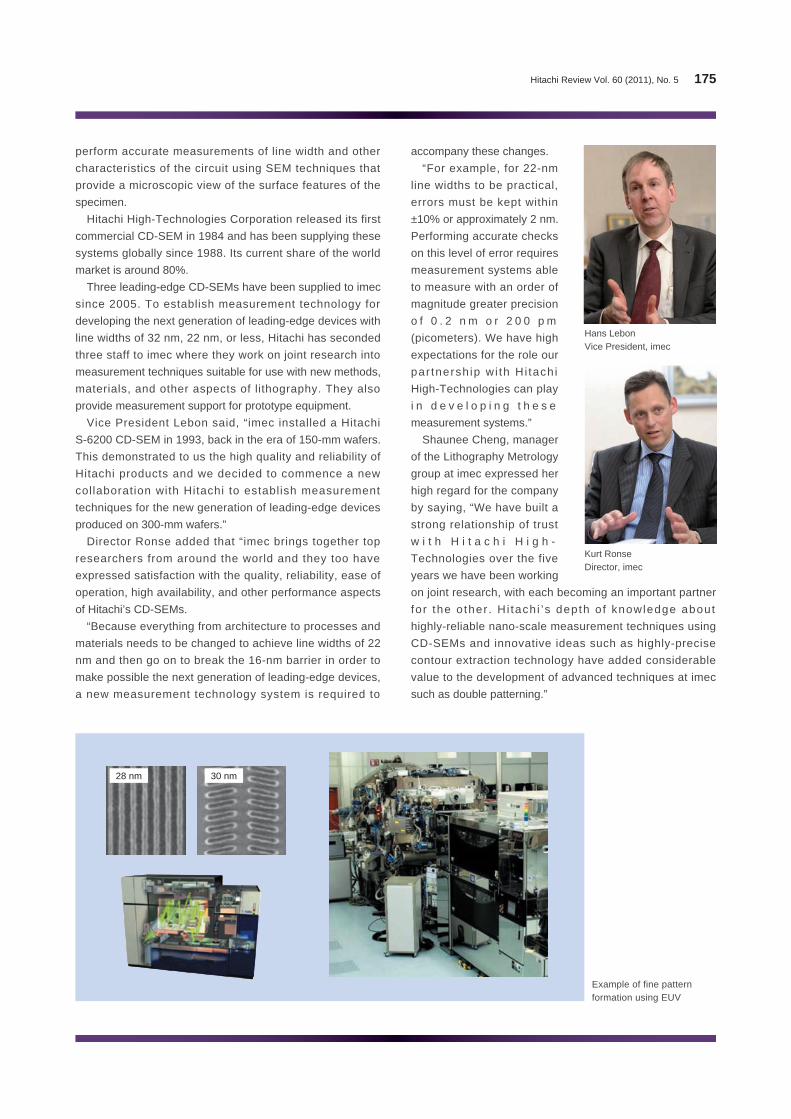
28 nm 30 nm
perform accurate measurements of line width and other characteristics of the circuit using SEM techniques that provide a microscopic view of the surface features of the specimen.
Hitachi High-Technologies Corporation released its first commercial CD-SEM in 1984 and has been supplying these systems globally since 1988. Its current share of the world market is around 80%.
Three leading-edge CD-SEMs have been supplied to imec since 2005. To establish measurement technology for developing the next generation of leading-edge devices with line widths of 32 nm, 22 nm, or less, Hitachi has seconded three staff to imec where they work on joint research into measurement techniques suitable for use with new methods, materials, and other aspects of lithography. They also provide measurement support for prototype equipment.
Vice President Lebon said, “imec installed a Hitachi S-6200 CD-SEM in 1993, back in the era of 150-mm wafers. This demonstrated to us the high quality and reliability of Hitachi products and we decided to commence a new collaboration with Hitachi to establish measurement techniques for the new generation of leading-edge devices produced on 300-mm wafers.”
Director Ronse added that “imec brings together top researchers from around the world and they too have expressed satisfaction with the quality, reliability, ease of operation, high availability, and other performance aspects of Hitachi’s CD-SEMs.
“Because everything from architecture to processes and materials needs to be changed to achieve line widths of 22 nm and then go on to break the 16-nm barrier in order to make possible the next generation of leading-edge devices, a new measurement technology system is required to
accompany these changes.“For example, for 22-nm
line widths to be practical, errors must be kept within ±10% or approximately 2 nm. Performing accurate checks on this level of error requires measurement systems able to measure with an order of magnitude greater precision o f 0 . 2 n m o r 2 0 0 p m (picometers). We have high expectations for the role our par tnersh ip wi th Hi tach i High-Technologies can play i n d e v e l o p i n g t h e s e measurement systems.”
Shaunee Cheng, manager of the Lithography Metrology group at imec expressed her high regard for the company by saying, “We have built a strong relationship of trust w i t h H i t a c h i H i g h - Technologies over the five years we have been working on joint research, with each becoming an important partner for the o ther . H i tach i ’s depth o f knowledge about highly-reliable nano-scale measurement techniques using CD-SEMs and innovative ideas such as highly-precise contour extraction technology have added considerable value to the development of advanced techniques at imec such as double patterning.”
Example of fine pattern formation using EUV
Hans Lebon Vice President, imec
Kurt Ronse Director, imec
175Hitachi Review Vol. 60 (2011), No. 5
At the seminar, Director Ronse presented research aimed at commercializing processing techniques for line widths of 22 nm or less using EUV. In conjunction with advances in measurement systems, how much further can nano-scale processing technology for semiconductors be taken?
Director Ronse replied by saying, “although various different ‘barriers’ have been proposed over the years in our field, new solutions have always been found and the obstacles overcome. I am confident that line widths down to 11 nm are practical using EUV lithography. I believe 7 nm is also possible but the huge cost of development required to achieve further miniaturization will mean that only a few companies will be able to take up this challenge. This gives imec an important role to play as a joint research institution. By conducting basic research and sharing the results with our partner companies, imec allows development to be done efficiently. We are currently working hard to find new solutions capable of performing measurements in the sub-10-nm range.”
How will sub-10-nm technology change devices and what possibilities will it open up?
Vice President Lebon replied that, “imec looks ahead to see what form society will take in the future and directs its research towards a reas o f m ic roe lec t ron i cs and nanotechnology that this society will require. Although it is up to imec’s partner companies to decide what sort of products they wish to produce using sub-10-nm devices, my view is that more advanced microprocessors and higher memory capacity will contribute in the consumer sector to d r a m a t i c a d v a n c e s i n m o b i l e e q u i p m e n t w i t h
comprehensive video functions such as smartphones, as well as more improvements to graphic processors, gaming, and other products.
“In the field of social infrastructure, I believe they will contribute to advanced information and telecommunication systems with low energy consumption and, in addition to enhancements to individual computers and storage systems, they will also contribute to progress in the field of cloud systems that l ink this equipment together into networks to provide advanced information services.”
On the subject of measurement systems for the next generation of lithography on which the burden of these expectations will be placed, Director Ronse said that, “What will be important in future is to seek out new measurement techniques capable of precise measurement of nano-scale patterning. This will require techniques able to perform precise measurements of the smal lest features of nano-scale pat terns and techniques for producing nano-scale patterning with high positional accuracy. I hope that we can continue to work on these challenges with Hitachi High-Technologies Corporation and share the experience we have buil t up through the successful collaborations conducted to date.”
Technology roadmap for semiconductor device miniaturization
ArF+RET
Cost/functions
Performance
ArF immersion
Double patterning
EUV lithography imec
Scaling
Time
Silicide
USJ
Strain
high-kHfO
Metal gate
Fin-FETCNT’
Ge/lllV Tunnel FET
45-32 nm
>65 nm
22 nm
Nanowire
<15 nm
Contribution to Sub-10-nm Processing
Scenes from Imec Executive Seminar 2010
176Special Report
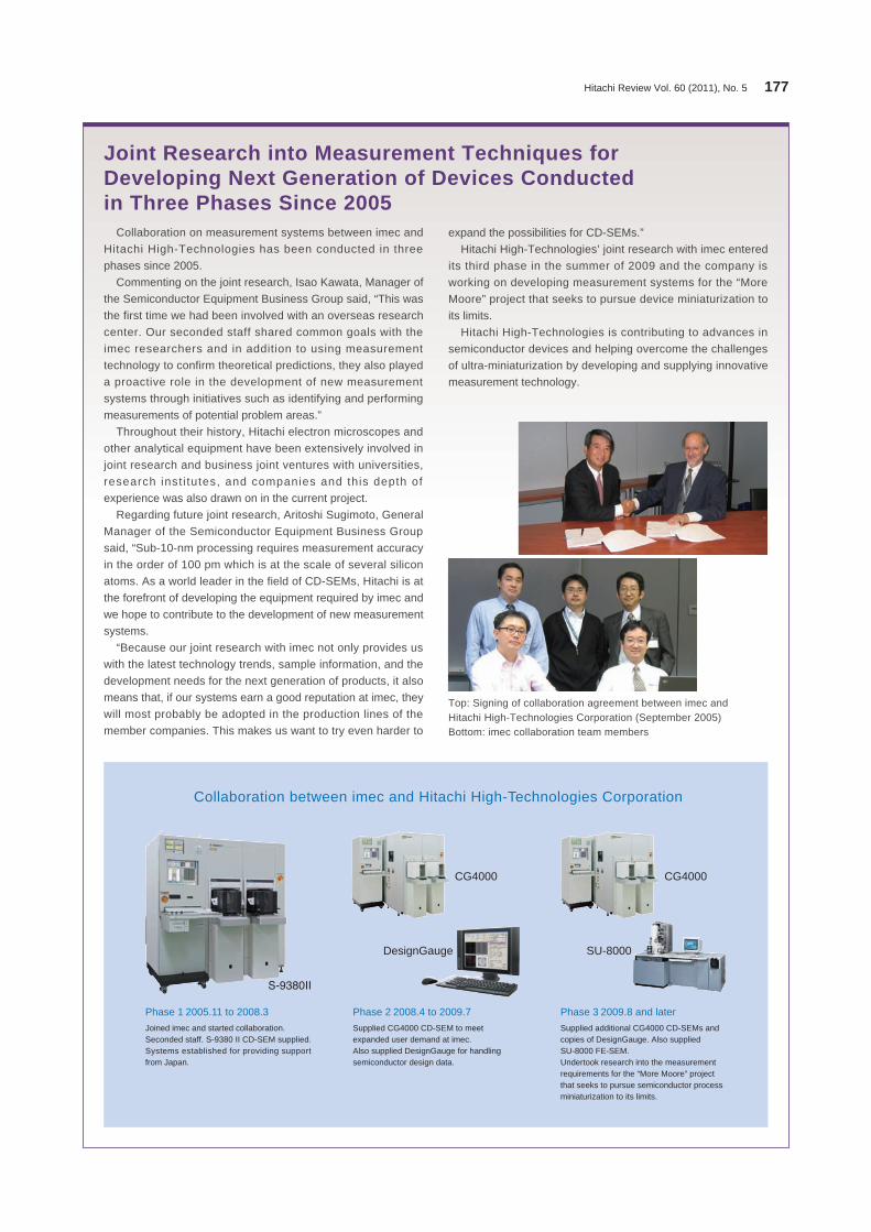
Collaboration on measurement systems between imec and Hitachi High-Technologies has been conducted in three phases since 2005.
Commenting on the joint research, Isao Kawata, Manager of the Semiconductor Equipment Business Group said, “This was the first time we had been involved with an overseas research center. Our seconded staff shared common goals with the imec researchers and in addition to using measurement technology to confirm theoretical predictions, they also played a proactive role in the development of new measurement systems through initiatives such as identifying and performing measurements of potential problem areas.”
Throughout their history, Hitachi electron microscopes and other analytical equipment have been extensively involved in joint research and business joint ventures with universities, research inst i tutes, and companies and this depth of experience was also drawn on in the current project.
Regarding future joint research, Aritoshi Sugimoto, General Manager of the Semiconductor Equipment Business Group said, “Sub-10-nm processing requires measurement accuracy in the order of 100 pm which is at the scale of several silicon atoms. As a world leader in the field of CD-SEMs, Hitachi is at the forefront of developing the equipment required by imec and we hope to contribute to the development of new measurement systems.
“Because our joint research with imec not only provides us with the latest technology trends, sample information, and the development needs for the next generation of products, it also means that, if our systems earn a good reputation at imec, they will most probably be adopted in the production lines of the member companies. This makes us want to try even harder to
expand the possibilities for CD-SEMs.”Hitachi High-Technologies’ joint research with imec entered
its third phase in the summer of 2009 and the company is working on developing measurement systems for the “More Moore” project that seeks to pursue device miniaturization to its limits.
Hitachi High-Technologies is contributing to advances in semiconductor devices and helping overcome the challenges of ultra-miniaturization by developing and supplying innovative measurement technology.
Phase 1 2005.11 to 2008.3 Phase 2 2008.4 to 2009.7 Phase 3 2009.8 and later
S-9380Ⅱ
CG4000
Collaboration between imec and Hitachi High-Technologies Corporation
CG4000
SU-8000DesignGauge
Joined imec and started collaboration.Seconded staff. S-9380 II CD-SEM supplied. Systems established for providing support from Japan.
Supplied CG4000 CD-SEM to meet expanded user demand at imec.Also supplied DesignGauge for handling semiconductor design data.
Supplied additional CG4000 CD-SEMs and copies of DesignGauge. Also supplied SU-8000 FE-SEM.Undertook research into the measurement requirements for the “More Moore” project that seeks to pursue semiconductor process miniaturization to its limits.
Joint Research into Measurement Techniques for Developing Next Generation of Devices Conducted in Three Phases Since 2005
Top: Signing of collaboration agreement between imec and Hitachi High-Technologies Corporation (September 2005)Bottom: imec collaboration team members


![arXiv:1605.09085v3 [cs.LG] 30 Aug 2019 · Maxim Berman KU Leuven, ESAT-PSI, imec, Belgium maxim.berman@esat.kuleuven.be Matthew B. Blaschko KU Leuven, ESAT-PSI, imec, Belgium matthew.blaschko@esat.kuleuven.be](https://static.documents.pub/doc/80x56/608c81ec78018f243e2a8fa3/arxiv160509085v3-cslg-30-aug-2019-maxim-berman-ku-leuven-esat-psi-imec-belgium.jpg)


