JOURNAL OF L A T E X CLASS FILES, VOL. 14, NO. 8, AUGUST 2015 1 Parallel Modular Scheduler Design for Clos Switches in Optical Data Centre Networks Paris Andreades, Student Member, IEEE, and Georgios Zervas, Member, IEEE Abstract—As data centers enter the exascale computing era their internal traffic, exchanged between network nodes, in- creases exponentially. Optical networking is an attractive solution to deliver the high capacity, low latency and scalable interconnec- tion needed. Amongst other switching methods, packet switching is particularly interesting as it can be widely deployed in the network to handle rapidly-changing traffic of arbitrary size. Nanosecond-reconfigurable photonic integrated switch fabrics, built as multi-stage architectures such as the Clos network, are key enablers to scalable packet switching. However, the accompanying control plane needs to also operate on packet timescales. Designing a central scheduler, to control an optical packet switch in nanoseconds, presents a challenge especially as the switch size increases. To this end, we present a highly-parallel, modular scheduler design for Clos switches along with a proposed routing scheme to enable nanosecond scalable scheduling. We implement our scheduler as an application-specific integrated circuit (ASIC) and demonstrate scaling to a 256 x 256 size with an ultra-low scheduling delay of only 6.0 ns. In a cycle-accurate rack-scale network emulation, for this switch size, we show a minimum end-to-end latency of 32.0 ns and maintain nanosecond average latency up to 80% of input traffic load. We achieve zero packet loss and short-tailed packet latency distributions for all traffic loads and switch sizes. Index Terms—IEEE, IEEEtran, journal, L A T E X, paper, tem- plate. I. I NTRODUCTION T HE global traffic within data centres is estimated to reach 14.7 zettabytes per year by 2021, driven by technology trends such as cloud computing and data centre virtualization [1]. Big data processing, workload migration, storage replication and retrieving data residing on multiple hosts are all examples of tasks that require data exchange between data centre machines [1]–[3]. The growth of this so called East-West traffic places stringent requirements on the network latency and bandwidth, causing a shift from the traditional hierarchical tree to the flatter leaf-spine network topology [4], [5], shown in Fig. 1. Optical fibre is typically installed between the leaf and spine layers to establish low loss and high bandwidth point-to-point connections. Nonetheless, the switches themselves are still electronic, limiting further performance scaling. Commercial electronic switches have a delay on the order of 200 ns [6] and limited capacity due to This work was supported by the UK Engineering and Physical Sciences Research Council (EPSRC) under Grant EP/R035342/1 and in part by the EU Horizon 2020 programme (Industrial Leadership section) under Grant 687632. Paris Andreades and Georgios Zervas are with the Electronic and Electrical Engineering Department, University College London (UCL), London, WC1E 7JE, UK (e-mail: [email protected], [email protected]). Manuscript received Month dd, yyyy; revised Month dd, yyyy. the number of high-speed pins available on the switch chip or the number of connectors fitting on a rack unit front panel [7]. These limitations can be addressed by optical switching reconfigurable in nanoseconds with orders of magnitude higher capacity, using wavelength-division multiplexing (WDM). Optical switches built as micro-electro-mechanical systems (MEMS) have been widely proposed for data centre networks. Notable examples include the RotorNet [8], c-Through [9], Helios [10], Proteus [11] and Mordia [12] prototypes. How- ever, because they are reconfigurable in milliseconds, they are used for circuit switching at the higher network layers where there is a larger traffic volume or in networks with slowly changing traffic. Hence, they are intended to be used alongside an electronic packet-switched network which would handle any bursty and rapidly-changing traffic. Moreover, their control plane needs to perform traffic demand estimation prior to circuit allocation to increase utilization [12], which could incur hundreds of milliseconds additional delay. Optical packet switching has also been proposed based on nanosecond-reconfigurable photonic integrated architectures built using micro-ring resonators [13], [14], semiconductor optical amplifiers (SOAs) [15], [16], Mach-Zehnder interfer- ometers (MZIs) [17] or a combination of these technologies [18]–[20]. Such switches could be deployed at any network layer without any limitation on the traffic size and stability. However, designing a switch control plane that operates on packet timescales, as the switch size scales, still remains a challenge in optical packet switch design. The Data Vortex [21], SPINet [22], OSMOSIS [23], the OPSquare switch as well as the work in [24], [25], all target scalable nanosecond switch control. In all cases, fast output-port arbitration for switch scheduling is key in implementing low-latency control. In previous work [26], we experimentally demonstrated a nanosecond control plane on field-programmable gate array (FPGA) boards. It enabled optical packet switching with a minimum 75 ns end-to-end latency in a 32-port SOA-crossbar system, for top-of-rack (ToR) application. In [27] a new output-port arbitration circuit for the switch scheduler was presented, doubling the switch size for the same scheduling delay. In [28], [29] we designed schedulers for optical switches built in a Clos network topology [30], as shown in Fig. 1, which is practical for photonic integration [31]. Also, this modular switch architecture enables scaling to large sizes while maintaining a low scheduling delay. This work expands on [29] by implementing the central Clos switch scheduler on hardware. Moreover, the scheduler was re- designed as a parallel and modular hardware structure to allow for clock speed optimization. The scheduler module designs
Transcript
JOURNAL OF LATEX CLASS FILES, VOL. 14, NO. 8, AUGUST 2015 1
Parallel Modular Scheduler Design forClos Switches in Optical Data Centre Networks
Paris Andreades, Student Member, IEEE, and Georgios Zervas, Member, IEEE
Abstract—As data centers enter the exascale computing eratheir internal traffic, exchanged between network nodes, in-creases exponentially. Optical networking is an attractive solutionto deliver the high capacity, low latency and scalable interconnec-tion needed. Amongst other switching methods, packet switchingis particularly interesting as it can be widely deployed in thenetwork to handle rapidly-changing traffic of arbitrary size.Nanosecond-reconfigurable photonic integrated switch fabrics,built as multi-stage architectures such as the Clos network,are key enablers to scalable packet switching. However, theaccompanying control plane needs to also operate on packettimescales. Designing a central scheduler, to control an opticalpacket switch in nanoseconds, presents a challenge especially asthe switch size increases. To this end, we present a highly-parallel,modular scheduler design for Clos switches along with a proposedrouting scheme to enable nanosecond scalable scheduling. Weimplement our scheduler as an application-specific integratedcircuit (ASIC) and demonstrate scaling to a 256 x 256 size withan ultra-low scheduling delay of only 6.0 ns. In a cycle-accuraterack-scale network emulation, for this switch size, we show aminimum end-to-end latency of 32.0 ns and maintain nanosecondaverage latency up to 80% of input traffic load. We achieve zeropacket loss and short-tailed packet latency distributions for alltraffic loads and switch sizes.
Index Terms—IEEE, IEEEtran, journal, LATEX, paper, tem-plate.
I. INTRODUCTION
THE global traffic within data centres is estimated toreach 14.7 zettabytes per year by 2021, driven by
technology trends such as cloud computing and data centrevirtualization [1]. Big data processing, workload migration,storage replication and retrieving data residing on multiplehosts are all examples of tasks that require data exchangebetween data centre machines [1]–[3]. The growth of thisso called East-West traffic places stringent requirements onthe network latency and bandwidth, causing a shift from thetraditional hierarchical tree to the flatter leaf-spine networktopology [4], [5], shown in Fig. 1. Optical fibre is typicallyinstalled between the leaf and spine layers to establish low lossand high bandwidth point-to-point connections. Nonetheless,the switches themselves are still electronic, limiting furtherperformance scaling. Commercial electronic switches have adelay on the order of 200 ns [6] and limited capacity due to
This work was supported by the UK Engineering and Physical SciencesResearch Council (EPSRC) under Grant EP/R035342/1 and in part by theEU Horizon 2020 programme (Industrial Leadership section) under Grant687632.
Paris Andreades and Georgios Zervas are with the Electronic and ElectricalEngineering Department, University College London (UCL), London, WC1E7JE, UK (e-mail: [email protected], [email protected]).
Manuscript received Month dd, yyyy; revised Month dd, yyyy.
the number of high-speed pins available on the switch chipor the number of connectors fitting on a rack unit front panel[7]. These limitations can be addressed by optical switchingreconfigurable in nanoseconds with orders of magnitude highercapacity, using wavelength-division multiplexing (WDM).
Optical switches built as micro-electro-mechanical systems(MEMS) have been widely proposed for data centre networks.Notable examples include the RotorNet [8], c-Through [9],Helios [10], Proteus [11] and Mordia [12] prototypes. How-ever, because they are reconfigurable in milliseconds, theyare used for circuit switching at the higher network layerswhere there is a larger traffic volume or in networks withslowly changing traffic. Hence, they are intended to be usedalongside an electronic packet-switched network which wouldhandle any bursty and rapidly-changing traffic. Moreover, theircontrol plane needs to perform traffic demand estimation priorto circuit allocation to increase utilization [12], which couldincur hundreds of milliseconds additional delay.
Optical packet switching has also been proposed based onnanosecond-reconfigurable photonic integrated architecturesbuilt using micro-ring resonators [13], [14], semiconductoroptical amplifiers (SOAs) [15], [16], Mach-Zehnder interfer-ometers (MZIs) [17] or a combination of these technologies[18]–[20]. Such switches could be deployed at any networklayer without any limitation on the traffic size and stability.However, designing a switch control plane that operates onpacket timescales, as the switch size scales, still remains achallenge in optical packet switch design. The Data Vortex[21], SPINet [22], OSMOSIS [23], the OPSquare switch aswell as the work in [24], [25], all target scalable nanosecondswitch control. In all cases, fast output-port arbitration forswitch scheduling is key in implementing low-latency control.
In previous work [26], we experimentally demonstrated ananosecond control plane on field-programmable gate array(FPGA) boards. It enabled optical packet switching with aminimum 75 ns end-to-end latency in a 32-port SOA-crossbarsystem, for top-of-rack (ToR) application. In [27] a newoutput-port arbitration circuit for the switch scheduler waspresented, doubling the switch size for the same schedulingdelay. In [28], [29] we designed schedulers for optical switchesbuilt in a Clos network topology [30], as shown in Fig. 1,which is practical for photonic integration [31]. Also, thismodular switch architecture enables scaling to large sizeswhile maintaining a low scheduling delay.
This work expands on [29] by implementing the central Closswitch scheduler on hardware. Moreover, the scheduler was re-designed as a parallel and modular hardware structure to allowfor clock speed optimization. The scheduler module designs
JOURNAL OF LATEX CLASS FILES, VOL. 14, NO. 8, AUGUST 2015 2
SPINE
LEAF
SOA
O/E E/On x m
NODES
SOA
O/E E/O 0
SOA
O/E E/O
SOA
O/E E/O 1
SOA
O/E E/O
SOA
O/E E/O r-1
0
r x rNODES
0
m x nNODES
1 1
r-1m-1
ToR
SERVERS
BUFFER
SCHEDULER
Fig. 1. A leaf-spine data centre with the proposed optical top-of-rack (ToR) Clos switch. Conversion from optical-to-electrical (O/E) and electrical-to-optical(E/O) enables electronic buffering at the switch inputs, when switch path contention occurs. The electronic scheduler processes switch path requests from thenetwork interfaces at the servers and at the switch buffers to reconfigure the optical switch in nanoseconds.
are presented and discussed in detail and are individuallysynthesized as application-specific integrated circuits (ASICs)in a 45 nm CMOS process. The results verify schedulinga 256 × 256 switch in 6.0 ns and identify the critical pathmodule, which determines the scheduler minimum clock pe-riod. That module is then implemented on a Xilinx Virtex-7XC7V690T FPGA board to compare our work with some ofthe fastest switch designs in the literature. The switch latencyand throughput performance are evaluated in a cycle-accurateemulation of our proposed system concept.
II. RELATED WORK
In this section we look at different notable schedulingapproaches to optical packet switch control from variousresearch labs in the field. The switch architecture is importantas it could simplify scheduling and reduce its impact on controldelay but at the same time it should not increase the dataplane complexity, hindering switch implementation. In gen-eral, scheduling can be executed centrally or in a distributedfashion, with the former usually considered to be of highcomplexity and incurring a considerable control plane delay.In this work, we aim to show otherwise. Table I compares thescheduling delay in different optical packet switches reportedin the literature.
The Data Vortex [21], [32] and SPINet [22], [33] designsdistribute scheduling to the 2×2 modules of an N×N banyannetwork, which scales by cascading log2N stages. Schedulingper module is executed in 10.0 ns but cascading them inmany stages increases total control delay and limits the switchthroughput at large sizes.
The OPSquare wavelength-routed switch [34]–[36] is alsomodular and scales by stacking modules in a 2-stage Spankearchitecture and by increasing the wavelength channels. Itavoids arbitration for the output modules by using wavelengthconversion. The arbitration time for the input modules dependson the number of wavelengths routed, bringing the total
scheduling delay to 25 ns, independent of switch size. How-ever, wavelength conversion and the high optical componentscount increase the implementation complexity and cost.
All aforementioned designs use in-band request schemeswhich have scheduling overheads for optical filtering, O/Econversion and request detection, in addition to arbitration.The design by Proietti et al. [24] avoids this by using opticalinstead of electronic scheduling. The switch is based onan N × N input-buffered arrayed waveguide grating router(AWGR) and scaling is determined by the highest port-countsupported by the AWGR technology. Scheduling is optical anddistributed to the output ports, where reflective semiconductoroptical amplification (RSOA) is used for nanosecond arbitra-tion, independent of N . However, scheduling is dominated bylaser tuning time (8 ns), switch round-trip time (5 ns) and grantdetection time (4 ns) at the input port. Also, arbitration fairnessis degraded, especially as N grows, compared to electronicround-robin schemes.
The central schedulers in the OSMOSIS prototype [23]and in the work by Cerutti et al. [25] use parallel iterativealgorithms to improve throughput in an N × N crossbarswitch at the cost of high scheduler complexity and longdelays. The scheduler design in our previous work [27], forcrossbar switches, trades off throughput for ultra-low delay;reconfiguring a 64× 64 crossbar in 18.8 ns. Nevertheless, anN × N crossbar is not practical for implementation at largesizes, due to the N2 switch elements required to built it.
All designs that issue an acknowledgement (ACK) from theswitch back to the packet source, whether in an optical orelectrical form, incur control overheads for ACK transport,detection and processing at the source, in addition to schedul-ing.
This work aims at a nanosecond-reconfigurable switch de-sign that scales both in the data plane and control plane. Itis based on a 3-stage Clos architecture and a novel routingscheme for simplified nanosecond scheduling and practical
JOURNAL OF LATEX CLASS FILES, VOL. 14, NO. 8, AUGUST 2015 3
OSMOSIS [23] - 51.2 ns - Crossbar Central Out-of-band Yes
Cerutti et al. [25] 1 µs - - Crossbar Central Out-of-band No
PACKETCONTROL
REQUESTCONTROL
λ1
λ2
λk
PACKET
t
REQUEST/FIFO FULL
RX
x N
SCHEDULER TO/F
RO
M S
PIN
E SW
ITCH
FRO
M S
ERV
ERTO
SER
VER
TX
N x NSWITCH
FIFO BUFFER
OPTICAL GATE ELECTRICAL DATA
CONTROLOPTICAL DATA
VOQs
Fig. 2. System concept. Server-side “send and forget” network interfaces andoptical top-of-rack (ToR) switch with input electronic buffers to avoid packetloss. Every transmitted packet is divided into k wavelengths to further reducelatency. The ToR scheduler reconfigures the switch in nanoseconds.
switch implementation. We can schedule a 256 × 256 Closswitch in just 6.0 ns in an ASIC implementation or in 21.0 nsin an FPGA implementation. The implementation resultsare presented in section V. Out-of-band electrical requests,processed by a central electronic scheduler, and speculativepacket transmission eliminate other control overheads besidesscheduling, as discussed in the next section.
III. SYSTEM CONCEPT
The proposed system concept is shown in Fig. 2. TheN × N optical top-of-rack (ToR) switch interconnects Nservers between themselves and to the spine switch. Internally,it is implemented as as Clos network. The server-side networkinterfaces implement a “send and forget” scheme wherebypackets are transmitted speculatively without a guaranteed paththrough the switch, reducing in this way the control latency.Hence, the optical Clos switch implements electronic bufferingat each input port to avoid packet loss for any failed pathspeculations, when at least two network interfaces contend fora switch path. The electronic scheduler processes path requeststo allocate switch paths, resolves contention where necessaryand reconfigures the optical switch to schedule traffic across it.In the next paragraphs the flow control is described in detail.
At every server network interface, the packets are initiallybuffered in a first-in, first-out (FIFO) policy. The request
control reads the destination of the head-of-line (HOL) packetand issues a switch path request to the scheduler.
Once the request is sent, the packet control holds onto theHOL packet for a configurable number of hardware clockcycles before forwarding it to the transceiver for transmis-sion. This allows for the scheduler to processes the requestand reconfigure the switch, before the packet arrives there.Nanosecond scheduler delay, tscheduler, is crucial for packetswitching. This delay is fixed, dependent on the schedulerdesign, and the main focus of this work is to optimize thedesign for ultra-low delay (< 10 ns), as the switch size scales.
Unlike circuit-switched systems, where a packet is bufferedat the source for possible retransmission until a path ACK(grant) is received, here every packet is forwarded to thetransceiver speculatively, without a scheduler grant. Comparedto the related work, this reduces the control delay by eliminat-ing the overheads for grant transport from the switch back tothe server network interface and then for synchronizing andprocessing it there. To avoid packet drop, in case of failedspeculation, buffering is used at each switch input port.
At the transceiver, every packet is divided into k seg-ments, each serialized at a fixed data rate onto a specificwavelength using, for example, a dedicated silicon photonictransceiver [37] integrated onto the network interface chip.Using wavelength-division multiplexing, the segments aretransmitted as one unit in a wavelength-parallel packet struc-ture to the switch input port, as shown in Fig. 2. This method,known as wavelength striping, increases the input port capacity(no. of wavelengths × data rate) and consequently reducesthe packet (de)serialization delay (packet size ÷ input portcapacity). More importantly, by dynamically reconfiguring thenumber of wavelength channels bonded, based on the packetsize, the system can support a low (de)serialization delay forvariable-size packets.
The resulting wavelength-striped packet is transmitted onthe WDM link to the switch input port, as shown in Fig. 2.In case of no switch path contention, hence no failed specu-lation, the wavelength-striped packet cuts through the alreadyreconfigured switch and is received at the destination with theminimum end-to-end latency. Otherwise, the packet is storedat the switch input port.
At every switch input port, buffering is implemented as Nparallel FIFO queues, one for each output port, also known
JOURNAL OF LATEX CLASS FILES, VOL. 14, NO. 8, AUGUST 2015 4
as virtual output queues (VOQs). Compared to using a singlequeue, the VOQ arrangement avoids the case where the HOLpacket, while waiting to be switched to its destination, blocksthe preceding packets in the queue even though they maybe destined elsewhere. Thereby, throughput is improved andbuffering delay is reduced, at the cost of increased schedulingalgorithm complexity. Optical to electrical (O/E) and electricalto optical (E/O) conversions are required when a packet isstored or released from a VOQ.
The central scheduler therefore receives two sets of pathrequests; one from the network interfaces at the servers, inresponse to new packets, and one from the network interfacesat the switch input ports (not shown in the diagram), inresponse to switch VOQ packets. Then, it arbitrates accessto switch paths, on round-robin basis, in parallel for the twosets and reconfigures the switch accordingly, including theVOQ control signals for storing and releasing packets. Priorityis always given to VOQ requests for strict in-order packetdelivery and low average latency.
As shown in Fig. 2, a “FIFO full” signal is asserted when aswitch VOQ is occupied beyond a threshold value, to notify thecorresponding server network interface to pause transmission(packets and requests). This provides control backpressure andenables managing a small VOQ size at the switch. For everyswitch input port there is an N -bit wide “FIFO full” bus,one bit for every VOQ, transmitted back to the server andoverall this is the only control signaling from the switch to theservers. The VOQ threshold value depends on the propagationdelay (tpropagation) between the switch and servers (round-trip) and also the scheduler delay (tscheduler) during whichthe server packets are buffered. The threshold value is givenby the following equation and determines the minimum VOQsize required to avoid packet loss up to 100% of traffic load:
Threshold = tscheduler + 2tpropagation (1)
In summary, the control plane latency is reduced by: (a) sched-uler design, (b) speculative transmission, (c) switch topologyand (d) switch routing. The average end-to-end latency isfurther reduced by having: (a) wavelength-striped packets and(b) virtual output queuing (VOQ) at the switch inputs. Thefocus of this work is the scheduler design, optimized for clockspeed and scalability.
IV. SCHEDULER DESIGN
The switch architecture or topology as well as the routingscheme directly affect the scheduler design and therefore thescheduling delay, tscheduler. In this work we design the sched-uler for a Clos network [30] used as the switch architectureand apply a fixed-path routing scheme, to reduce the schedulerdelay and also simplify its design.
A Clos network is built using strictly non-blocking switch-ing modules arranged in a multi-stage topology. A 3-stageClos network is characterized by the triple (m,n, r), where mis the number of central modules (CMs), n is the number ofinput (output) ports on each input (output) module and r is thenumber of input modules (IMs) and output modules (OMs),as shown in Fig. 3. In an N×N Clos switch, N = n×r. The
n x m
Input Modules
r x r
Central Modules
m x n
Output Modules
n
n
0
1
r-1
0
1
m-1
0
1
r-1
Fig. 3. An (m,n,r) Clos network built with strictly non-blocking modules.The proposed routing scheme, for m = n = r Clos networks, assigns fixedpaths to avoid contention at the central modules, simplifying the schedulerdesign and reducing its delay.
case where m = n = r =√N , is attractive for photonic
integration [31] and it gives a re-arrangeably non-blockingnetwork, given an appropriate routing algorithm is used. Moreimportantly, the modular structure of Clos networks enablesreducing the scheduler delay because only
√N -bit arbitration
circuitry would be needed per module, for distributed pathallocation.
Any multi-stage architecture, such as the Clos network,requires a routing algorithm. In the Clos network there are mpaths from any input port, i, to any output port, j. The loopingalgorithm [38] can be used for Clos networks with m = n; ititerates the routing matrix, re-arranging current entries to addnew routes, without blocking others. Iterating would cause along scheduling delay, limiting scalability.
In this design, the routing algorithm assigns fixed paths tominimize the routing overhead. Furthermore, it completelyeliminates contention at the central modules, as shown inFig. 3. Since there is no need to arbitrate for any of the centralmodules, the scheduler design is simplified, less hardwareresources are required and delay is further reduced. The tradeoff is that the architecture becomes blocking; at every IM atmost one input port can be allocated the route to an OM, evenif different output ports on that OM are requested. Hence, theswitch throughput will saturate at a lower input traffic loadcompared to using the looping algorithm, for a given switchsize. Switch average throughput measurements are presentedin section VI.
The fixed path assignment could also be used to simplify theswitch design. Since there is no switching activity at the centralmodules, these can be removed resulting in a 33% reductionin cross-points and 50% reduction in waveguides, improvingsignal integrity and reducing the power requirement. Thismakes the switch more practical to implement as a photonic-integrated circuit.
Figure 3 shows how the routing algorithm assigns the firstpath (CM 0), at every IM. More specifically, at every IM,the first path/output port leads to a different OM to avoid
JOURNAL OF LATEX CLASS FILES, VOL. 14, NO. 8, AUGUST 2015 5
OM
Allocator
(1)
OM
Allocator
(r-1)
OP
Allocator
(0)
OP
Allocator
(1)
OP
Allocator
(r-1)
OM
Allocator
(0)
SW
ITC
H C
ON
FIG
UR
AT
ION
Input
Modules
Output
Modules
Fig. 4. Central Clos switch scheduler implemented in a planar and modularfashion. Planes operate independently and in parallel to allocate paths basedon output module (OM) and output port (OP) arbitration for the Clos inputand output modules. The switch configuration module reconfigures the switchbased on the path allocation results from both planes.
contention at CM 0. This is the case for the remaining pathsassigned. At any given IM, the path assignment to the OMsis a circular shift by one position to the left, with respect tothe previous IM. It is calculated based on the input port (i)and destination output port (j) associated with every packet,according to the following equation:
p(i, j) = (bi/nc+ bj/rc) mod m (2)
where 0 ≤ i, j ≤ N − 1.Since there can be no contention at the central modules,
path allocation is implemented as output port arbitration forevery input and output module. This translates to allocatingOMs to the IM input ports and then allocating OM outputports to the IMs.
The central scheduler is implemented in a modular planarapproach as illustrated in Fig. 4. This allowed optimisation forclock speed. There are two parallel path-allocation planes, oneresponsible for processing new packet (server) requests andone for processing VOQ packet (switch) requests. On eachplane, there are r allocation modules for the Clos IMs andanother r allocation modules for the Clos OMs, arranged intwo ranks and interconnected in a full mesh topology. Theswitch configuration module processes the allocation resultsfrom both planes to produce the configuration control signalsfor the Clos input and output modules. Every allocationmodule or allocator, irrespective of rank and plane, makesdecisions based on a group of round-robin arbiters, whereevery arbiter is designed as outlined in [39]. In the nextsections, we present the output module (OM) allocator designfor each plane, the output port (OP) allocator design commonto both planes and the switch (re)configuration design.
A. Output Module Allocation for New Packets
The allocator design for an n × r IM, for new packetrequests, is shown in Fig. 5. For every new packet arrivingat an input port, there is a switch output port request basedon the packet’s destination. The circuit processes every request
/Arbiter
0
Arbiter
1
Arbiter
r-1
/n
Input Port
Selection
/n
/n
/n
/n
/n
x r
x r
log2(N)+1
/n
Gj
Gi
log2(N)+1
/
x n
N
/
x nRS
R
A B
Re
qu
est
Lo
gic
Gra
nt
Lo
gic
Fig. 5. Output module allocator design for new packet requests. The criticalpath in the design is shown in red. Tags A and B are for cross-reference withthe example in Fig. 6.
0 0 1 0
0 0 0 0
0 0 1 0
0 1 0 0
Output
Module
0 0 1 0
0 0 0 0
0 0 0 0
0 1 0 0
Output
Module
Gj
Outp
ut
Module 0 0 0 0 0
1 0 1 0 0
2 0 0 1 0
3 0 0 0 0
Output
Port
Gi
Outp
ut
Module 0 0 0
1 7 1
2 4 1
3 0 0
Input
Port
v
RS
InputP
ort
4 0 0 0 0 0 0 0 0 0 0 0 0 0 0 0 0
5 0 0 0 0 1 0 0 1 0 0 0 0 0 0 0 1
6 0 1 0 0 0 0 0 0 0 0 0 0 0 0 0 0
7 0 0 0 0 1 0 0 0 1 0 0 0 0 0 0 0
R
Input
Port
4 10 1
5 4 1
6 8 1
7 5 1
Output
Port
v
A B
12840Output Port
01
23
OM0
45
67
OM1
OM2 10
11
98
Fig. 6. Example request processing for new packets by the output moduleallocator for the 2nd input module in a (4,4,4) Clos switch. Binary matricesare tagged for cross-reference with the digital design in Fig. 5.
and attempts to match each input port to the OM on which therequested output port physically resides. There are two sets ofinput requests to the circuit: (a) n requests for the new packets,in matrix R, and (b) n requests for VOQ packets at the IMinput ports, in matrix RS . The VOQ requests are high-priorityand are used here only to filter out new packet requests thatthey are contending against for IM input ports. This maintainsstrict in-order packet delivery. For the filtered out requests, thecorresponding packets arriving at the switch are stored in theappropriate VOQs.
Every request in R is a structure with two fields; the switchdestination port, represented by log2N bits, and a valid bit.Every request in RS is an N -bit vector, where every bitasserted represents a request for the output port that the VOQbuffers packets.
The request logic checks RS to determine whether a newpacket contends with a VOQ packet for an IM input port,in which case the new packet request is dropped. Then, itgenerates a request in a format that the subsequent arbiterlogic can process; based on a new packet’s destination port ann-bit request for the destination OM is generated, where eachbit asserted is an IM input port requesting that OM. There arer arbiters, each allocating an OM to at most one of n requests,based on the round-robin principle. Each arbiter outputs a one-hot n-bit grant indicating the winning IM input port.
JOURNAL OF LATEX CLASS FILES, VOL. 14, NO. 8, AUGUST 2015 6
/
RS
Arbiter
1
Arbiter
n-1
Arbiter
1
Arbiter
r-1
Arbiter
0
Re
qu
est
Lo
gic Arbiter
1
Arbiter
r-1
/r
OM
Selection
Input Port
Selection
/n
/n
/n
Output Port
Selection
Gra
nt
Lo
gic
/n
/n
/n
/n
/n
/n
/n
/n
/r
/r
/
x r
x r
log2(N)+1
/n
Gj
Gi
/N
/N
/N
Re
qu
est
Lo
gic
N
/N
/N
x n
Arbiter
0
Arbiter
0
A B C D E
Fig. 7. Output module allocator design for switch VOQ packet requests. The critical path in the design is shown in red. Tags A-E are for cross-referencewith the example in Fig. 8.
RS
Inp
ut
Po
rt
4 0 0 0 0 0 0 0 0 0 0 0 0 0 0 0 0
5 0 0 0 0 1 0 0 1 0 0 0 0 0 0 0 1
6 0 1 0 0 0 0 0 0 0 0 0 0 0 0 0 0
7 0 0 0 0 1 0 0 0 1 0 0 0 0 0 0 0
Inpu
tP
ort
4 0 0 0 0
5 0 1 0 1
6 1 0 0 0
7 0 1 1 0
Output
Module
Ou
tput
Mod
ule 0 0 1 0 0
1 1 0 0 1
2 0 0 0 0
3 0 0 0 0
Output
Port
Gi
Ou
tput
Mo
du
le 0 6 1
1 5 1
2 0 0
3 0 0
Input
Port
v
Gj
0 1 0 0
1 0 0 0
0 0 0 0
0 0 0 0
Output
Port
0 0 0 0
0 1 0 0
1 0 0 0
0 0 0 0
Output
Module
0 0 0 0
0 1 0 0
1 0 0 0
0 1 0 0
Output
Module
12840Output Port
EDCBA
01
23
OM0
45
67
OM1
0 1 0 0
1 0 0 0
0 0 0 0
0 0 0 0
Output
Port
Fig. 8. Example request processing for switch VOQ packets by the outputmodule allocator for the 2nd input module in a (4,4,4) Clos switch. Binarymatrices are tagged for cross-reference with the digital design in Fig. 7.
The grant logic generates the circuit’s output matrices, Gi
and Gj , based on the arbiter grants. Each matrix has at mostr grants, one for every Clos OM. Every grant in Gi is astructure with an input-port field of log2N bits and a validbit, to indicate the switch input port granted that OM. EveryGj grant is a one-hot n-bit vector and the bit asserted, if any,indicates the granted output port on that OM. Every valid grantpair, one from Gi and one from Gj , forms a request that thededicated output port (OP) allocator on the same plane willprocess next, as illustrated in Fig. 4.
Figure 6 shows an example of the circuit functionality for a(4, 4, 4) Clos, for a given R and RS . The requests processedin the example are for the second input module (IM 1) whoseinput ports are in the range 4 to 7. The request logic is showngenerating a binary matrix containing the arbiter requests,ignoring input port 5’s request as it contends with a VOQrequest for the same input and output ports. Next, every arbiterresolves any OM contention by operating across a matrixcolumn, selecting only one input port for that OM. The outputmatrices Gi and Gj are created based on the arbitration results.
B. Output Module Allocation for Switch VOQ Packets
In an n×r IM, due to VOQ buffering, there could be up toN switch output port requests per input port, at the same time.For every input port, the OM allocator grants at most one ofr OMs, for a selected output port. This design is only used inthe scheduler plane responsible for VOQ request processing,as illustrated in Fig. 4. As shown in Fig. 7, the design is
divided in two pipeline stages to increase the maximum clockfrequency achievable.
Every input request in RS is an N -bit vector. This is thesame input matrix in the allocator for new packet requestsdescribed above. In the first pipeline stage, the request logicgenerates the arbiter input requests; n r-bit vectors in whichevery bit asserted is a request for an OM.
Next, input-first separable allocation is performed to matchoutput modules with the local input ports. Separable allocationis performed as two sets of arbitration; one across the inputports and one across the output modules. This is implementedas two separate arbiter ranks. The first rank has n r-bit arbitersto select one OM for every input port. The second rank has rn-bit arbiters to select one input port for every OM.
The iSLIP method [40], for round-robin separable alloca-tion, is used to increase the number of grants. This is doneby controlling the arbiter priority in the first rank so that itis less likely different arbiters select the same output module,causing fewer conflicts in the second arbiter rank. Althoughmultiple iterations can be performed, to further increase thenumber of grants and therefore the switch throughput, only asingle pass (1-SLIP) is executed to minimize the total circuitdelay. To implement iSLIP, the priority of a first-rank arbiter isupdated only if its grant output has also won arbitration in thesecond arbiter rank. However, this creates a feedback whichforms the critical path in the design, as discussed in section V.Any first-rank arbiter receives r feedback signals in total, onefrom each second-rank arbiter, but only the feedback betweenthe first two arbiters is shown in in Fig. 7, for diagram clarity.
In the case of switch VOQ packets, since there can bemore than one output port request per OM, an additionalround of arbitration is needed to select one, after an input porthas been granted an OM. This is implemented in the secondpipeline stage. Based on the OM allocation grants from thefirst pipeline stage, the request logic creates n-bit requests,for every granted OM, and the following arbiters select one.Effectively the two allocation rounds operate in a master-slavefashion divided in two pipeline stages.
In the same way as in the allocator for new packet re-quests, the grant logic generates two matrices, Gi and Gj ,each holding a grant for every Clos output module that thecorresponding output port (OP) allocator will process.
An example of the circuit functionality is shown in Fig. 8.
JOURNAL OF LATEX CLASS FILES, VOL. 14, NO. 8, AUGUST 2015 7
//
Arbiter
0
Arbiter
1
Arbiter
n-1
IM
Selection
Gra
nt
Lo
gic
/log2(N)+1
OM
Sta
te
n
/n
/r/
r/r
/r
/r
/r
/r
OP
Sta
te
/r
/n
x N
SOM
SOP
Gx rx r
log2(N)+1
/
/
/
x r
n
n
n
Re
qu
est
Lo
gic
IP
Lo
gic
Gi
Gj
A
B C
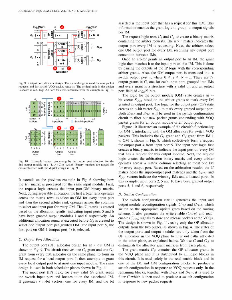
Fig. 9. Output port allocator design. The same design is used for new packetrequests and for switch VOQ packet requests. The critical path in the designis shown in red. Tags A-C are for cross-reference with the example in Fig. 10.
Gi
OM
Input
Port
12 1 3
Input
Module
2 1 0
5 1 1
10 1 2
Switch
In. Port
v
Gj
OM
Input P
ort
1 0 0 0 3
Input M
odule
0 1 0 0 0
1 0 0 0 1
0 0 1 0 2
4 5 6 7
Output
Port
Input M
odule 0 0 0 1 0
1 0 1 0 0
2 0 0 1 0
3 1 0 0 0
OM
Input Port
Input M
odule 0 0 1 0 0
1 1 0 0 0
2 0 0 1 0
3 1 0 0 0
4 5 6 7
Output
Port
SOM
Input M
odule 0 1
1 1
2 1
3 0
SOP
Outp
ut
Port 4 1
5 1
6 1
7 0
A
B
0 1 0 0
1 0 0 0
0 0 1 0
0 0 0 0
4 5 6 7
Output
Port
C
G
0 0 1 0 0 1 0 0 0 0 1 0 0 0 0 0 v
0 0 5 0 0 4 0 0 0 0 6 0 0 0 0 0
Outp
ut
Port
12840
Switch Input Port
Fig. 10. Example request processing by the output port allocator for the2nd output module in a (4,4,4) Clos switch. Binary matrices are tagged forcross-reference with the digital design in Fig. 9.
It extends on the previous example in Fig. 6 showing howthe RS matrix is processed for the same input module. First,the request logic creates the input port-OM binary matrix.Next, during separable allocation, the first arbiter rank operatesacross the matrix rows to select an OM for every input portand then the second arbiter rank operates across the columnsto select one input port for every OM. The Gi matrix is createdbased on the allocation results, indicating input ports 5 and 6have been granted output modules 1 and 0 respectively. Anadditional allocation round is executed before Gj is created toselect one output port per granted OM. For input port 5, thefirst port on OM 1 (output port 4) is selected.
C. Output Port Allocation
The output port (OP) allocator design for an r × n OM isshown in Fig. 9. The circuit receives one Gi grant and one Gj
grant from every OM allocator on the same plane, to form anIM request for a local output port. It then attempts to grantevery local output port to at most one input module. The samedesign is used in both scheduler planes shown in Fig. 4.
The input port (IP) logic, for every valid Gi grant, readsthe switch input port and locates it on the associated IM.It generates r n-bit vectors, one for every IM, and the bit
asserted is the input port that has a request for this OM. Thisinformation enables the grant logic to group its output signalsper IM.
The request logic uses Gi and Gj to create a binary matrixcontaining the arbiter requests. The n× r matrix indicates theoutput port every IM is requesting. Next, the arbiters selectone OM output port for every IM, resolving any output portcontention between IMs.
Once an arbiter grants an output port to an IM, the grantlogic then matches it to the input port on that IM. This is doneby pairing the outputs of the IP logic with the correspondingarbiter grants. Also, the OM output port is translated into aswitch output port j, where 0 ≤ j ≤ N − 1. There are Noutput grants in G, one for each input port, grouped into IMsand every grant is a structure with a valid bit and an outputport field of log2N bits.
The logic for the output module (OM) state creates an r-bit vector SOM based on the arbiter grants to mark every IMgranted an output port. The logic for the output port (OP) statecreates an n-bit vector SOP to mark every granted output port.Both SOM and SOP will be used in the switch configurationcircuit to filter out new packet grants contending with VOQpacket grants for an output module or an output port.
Figure 10 illustrates an example of the circuit’s functionalityfor OM 1, interfacing with the OM allocators for switch VOQpackets. This includes the Gi grant and Gj grant from IM 1to OM 1, shown in Fig. 8, which collectively form a requestfor output port 4 from input port 5. The input port logic firstcreates a binary matrix to indicate the input port on every IMthat has a request for this output module. Next, the requestlogic creates the arbitration binary matrix and every arbiteroperates across a matrix column selecting at most one IMfor every output port. Based on the arbitration results, the Gmatrix holds the input-output port matches and the SOM andSOP vectors indicate the winning IMs and allocated ports. Inthis example, input ports 2, 5 and 10 have been granted outputports 5, 4 and 6, respectively.
D. Switch ConfigurationThe switch configuration circuit generates the input and
output module reconfiguration signals, CIM and COM , whichswitch on the appropriate optical gates based on the routingscheme. It also generates the write-enable (CWE) and read-enable (CRE) signals to store and release packets at the VOQs.The design is shown in Fig. 11, using only the OP allocatoroutputs from the two planes, as shown in Fig. 4. The states ofthe output ports and output modules are only taken from theOP allocators in the VOQ plane to filter out paths allocatedin the other plane, as explained below. We use G and GS todistinguish the allocator grant matrices from each plane.
The grant matrix GS contains the OP allocator grants inthe VOQ plane and it is distributed to all logic blocks inthis circuit. It is used solely in the read-enable block and inone of the IM and OM configuration blocks, to produce aswitch configuration in response to VOQ requests only. In theremaining blocks, together with SOM and SOP , it is used tofilter G which is then used to produce a switch configurationin response to new packet requests.
JOURNAL OF LATEX CLASS FILES, VOL. 14, NO. 8, AUGUST 2015 8
/log2(n)+1
x N
/log2(n)+1
x N
Co
mb
ine
r
/
x N
log2(n)+1
x N
/log2(r)+1
x N
/log2(r)+1
x N
/
x N
log2(r)+1
x N
/
x N
/
x N
/
x r
/
x r
IM
CNFG
IM
CNFG
OM
CNFG
Read-
Enable
Grant
Logic
OM
CNFG
log2(N)+1
log2(N)+1
r
n
x N
x N
log2(N)+1
GS
G
SOM
SOP
COM
CIM
CWE
CRE
/
log2(N)+1/
Co
mb
ine
r
Fig. 11. Switch configuration circuit. Blue-coded logic blocks are for VOQrequests and otherwise for new requests. The critical path in the design isshown in red.
The read-enable logic transfers GS directly to the outputregister for the VOQ read-enable signals in CRE . In total thereare N signals, one for every switch input port, where eachsignal is a structure with a valid bit and log2(N) bits to addresseach VOQ. A valid read-enable signal releases a packet fromthe corresponding switch VOQ at an input port.
The IM and OM configuration logic blocks for VOQ re-quests, shown in blue color in Fig. 11, generate a configurationsignal for every valid grant in GS . An IM configuration signaluses log2(n) bits to identify one out of n optical gates on anIM output port to turn on. Similarly, an OM configurationsignal uses log2(r) bits to identify one out of r optical gateson an OM output port to turn on.
At the grant logic, every valid grant in G is passed to theoutput only if: (a) no GS grant is valid for that IM input port,(b) the destination OM is free for that IM, according to SOM
and (c) the destination output port j is free, according to SOP .This 3-condition filter gives priority to VOQ packets. Anygrant passing through the filter corresponds to a new packetbeing switched with the minimum latency. The outputs areinverted and registered to produce the write-enable signals inCWE , where a valid signal stores a new packet in the switchVOQ addressed by log2(N) bits.
The IM and OM configuration logic for new packets gener-ates a configuration signal for every valid grant in G, given thatgrant also passes through the same 3-condition filter used inthe grant logic. The IM configuration signals for new packetsand VOQ packets are then combined together into a single setof N signals before they are registered out as CIM . In thesame way, the output OM configuration, COM , is generatedby combining the configuration signals for new packets andswitch VOQ packets.
In this section we discuss the implementation of the mod-ular scheduler design on hardware. More specifically, everyhardware module described in the previous section has beenimplemented separately as an application-specific integratedcircuit (ASIC), in a 45 nm CMOS process. The critical pathin each module is identified and measured to determine theminimum clock period that the scheduler, as a whole unit,can achieve. The modules are also implemented on a Virtex-7 XC7V690T FPGA board to investigate how the schedulerprototype compares to our previous work and to related workin the literature. Carry-look-ahead was used for the round-robin arbiters in the allocator modules for the 64-port and 256-port scheduler, both in the FPGA and ASIC implementation.
A. Application-Specific Integrated Circuit (ASIC)
The critical path, for every scheduler component, is shownin its circuit diagram in section IV. Table II lists the corre-sponding minimum clock period for the ASIC implementation.The longest critical path is in the output module allocatorfor switch VOQ packets. It falls in the first pipeline stageresponsible for the iSLIP allocation. It extends from therequest register through a cascade of two iSLIP arbiters andthen back to the priority register of the first arbiter, as shownin Fig. 7. This sets the minimum clock period, Tscheduler, forthe entire scheduler at 2 ns for a 256× 256 Clos switch.
According to Table II, the increase in minimum clockperiod, as the switch quadruples in size, is sublinear for allscheduler modules, demonstrating a scalable scheduler design.The OM allocator for new packets and the OP allocator usesame size arbiters, request and grant logic, hence the criticalpath is of the same length. Moreover, there is only a smalldifference in minimum clock period between the differentscheduler components, for the same switch size, indicatingan overall pipelining balance in the scheduler design. As wereported in [29], the entire scheduler can be implemented asa 3-stage pipelined circuit, in which case its total delay, for a256×256 switch, would be tscheduler = 3×Tscheduler = 6 ns.In a synchronous rack-scale (2 m) system, the total controlplane delay would be less than 20 ns, including requestgeneration (2 ns), propagation to scheduler (10 ns), scheduling(6 ns) and SOA-based switch reconfiguration (0.115 ns [41]).
B. Field-Programmable Gate Array (FPGA)
The iSLIP output module allocator was implemented onthe Xilinx Virtex-7 XC7V690T FPGA board to compare the
JOURNAL OF LATEX CLASS FILES, VOL. 14, NO. 8, AUGUST 2015 9
TABLE IIIMINIMUM CLOCK PERIOD FOR FPGA IMPLEMENTATION
scheduler delay to ASIC implementation, previous work andalso to related work in the field. The critical path in theallocator is the same as in the ASIC implementation.
Table III lists the minimum clock period for differentswitch sizes. As the switch quadruples in size, the minimumclock period again shows a sublinear increase, which verifiesscheduler scalability. Compared to the ASIC OM allocator inTable II, the scheduler would run 2.6 to 3.5 times sloweron the FPGA board as the switch radix is increased from16 to 256, respectively. However, against the Clos schedulerdesign in previous work [28], a switch twice the size cannow be scheduled 16.7% faster. This is due to distributedpath allocation and routing scheme. The total scheduler delay,compared to ASIC implementation and other related work, islisted in Table I in section II.
VI. NETWORK EMULATION RESULTS
A network emulator was built to evaluate the switch per-formance under the control of the scheduler in our systemconcept, described in section III. The emulator was developedin SystemVerilog, a hardware description language (HDL) fordigital design and hardware implementation, and ran in MentorGraphics ModelSim. Using an HDL emulator allows for cycle-accurate measurements. The emulator consists of N packetsources, the network model and the packet sink, arranged asshown in the block diagram in Fig. 12.
Each packet source injects traffic with a uniform randompacket inter-arrival and the injection probability is set by auniversal load parameter. The packets are timestamped in theclock cycle they are generated. Also, the packet destinations(switch output ports) are random and uniformly distributed.
The network model implements an N ×N optical switch,the switch scheduler, N server network interfaces each witha single FIFO queue and another N network interfaces forthe switch input ports each with N FIFO virtual outputqueues (VOQs). Every packet source feeds one server networkinterface. The packet sink receives all output packets from theswitch instance, adds a second timestamp to each packet andperforms all necessary measurements.
The emulation captures the end-to-end latency in our systemconcept, shown in Fig. 2. It includes control plane overheadsfor request control (TTX ), transport (tpropagation) and schedul-ing (tscheduler) as well as data plane overheads for packetbuffering, transport (tpropagation), de-serialization (tserial) andswitch reconfiguration (tswitch).
The emulation parameters are listed in Table IV. The(m,n, r) Clos configurations considered for the switch ar-chitecture are the (4,4,4), (8,8,8) and (16,16,16) for sizes16× 16, 64× 64 and 256× 256. Built using SOA technology,
N x N Network
Data Plane
Control Plane
Switch Scheduler
Packet Sink
Packet SourceTraffic Gen
TXCount
TimeStamp
RXCount
Per
form
ance
Cal
cula
tio
n
PathAllocation
SwitchConfiguration
Request Control
Packet Control
Congestion Control
Request Transport Delay
Switch Configuration Delay
Buffering Delay
Packet Serialization Delay
TimeStamp
x N
Packet Transport Delay
Fig. 12. The network emulation setup.
TABLE IVNETWORK EMULATION PARAMETERS
Parameter Value
Measurements Duration 20 µs
Switch Size - N 16, 64, 256
Tscheduler (ASIC) 1.1 ns, 1.4 ns, 2.0 ns
TTX Tscheduler
tswitch (SOA Rise Time) 0.115 ns
tserial (k× 100 Gb/s) Tscheduler - tswitch
tpropagation (2 m) 10 ns
the reconfiguration time, tswitch, can be as low as 115 ps[41]. The clock period, TTX , at which the packet sourcesand server network interfaces are running, is equal to thescheduler clock period, Tscheduler, for a synchronous system.The packets are assumed to be wavelength-striped across kwavelengths each running at 100 Gb/s, with a de-serializationlatency, tserial ≤ Tscheduler − tswitch. The propagation delay(tpropagation) is set to 10 ns to model a rack-scale system with2 m link distances.
Figure 13 shows the average end-to-end latency against theinput traffic load, as a percentage of capacity, for differentsize Clos switches and ASIC scheduler. At low loads, theaverage end-to-end latency for each switch size convergesto the minimum value; it consists of 1 TTX buffer controldelay at the packet source and server network interface, re-quest propagation (tpropagation) to the scheduler, 3 Tscheduler
scheduling, switch reconfiguration (tswitch), packet propa-gation (tpropagation) to the receiver and finally packet de-serialization (tserial) at the receiver. The minimum latencyis longer for larger switches, due to longer Tscheduler, and isgiven by the following equation:
t = 2TTX +2tpropagation+ tscheduler + tswitch+ tserial (3)
where tscheduler = 3 × Tscheduler. For the 256-port switch,t = 32.0 ns out of which 20 ns is due to 2×10 m propagation.Clock and data recovery (CDR) at the receiver is excluded but
JOURNAL OF LATEX CLASS FILES, VOL. 14, NO. 8, AUGUST 2015 10
0 10 20 30 40 50 60 70 80 90 100
Input Traffic Load (% Capacity)
101
102
103
104
Avera
ge E
nd
-to
-En
d L
ate
ncy (
ns)
16x16
64x64
256x256
Fig. 13. Average end-to-end latency vs. input traffic load, for different sizeClos switches. Results are based on scheduler implementation on 45 nmCMOS ASIC. The network emulation assumes uniform random traffic andwavelength-striped packets of at most 1 clock cycle duration. A 2 m fibredistance to and from the switch is assumed to model rack-scale switching.
0 10 20 30 40 50 60 70 80 90 100
(a)
0
4
8
0 10 20 30 40 50 60 70 80 90 100
(b)
0
4
8
Lo
g2V
OQ
Siz
e (
Packet
En
trie
s)
0 10 20 30 40 50 60 70 80 90 100
(c)Input Traffic Load (% Capacity)
0
4
8
Fig. 14. Minimum switch VOQ size vs. input traffic load, for (a) 16 x 16, (b)64 x 64 and (c) 256 x 256 Clos switch sizes. Results are based on schedulerimplementation on 45 nm CMOS ASIC. The network emulation assumesuniform random traffic and wavelength-striped packets of at most 1 clockcycle duration.
the overhead will not be significant, given the sub-nanosecondCDR time reported in [42].
For all switch sizes, as the traffic load is increased, thecontention probability in the Clos switch increases and morepackets are buffered at the switch, which in turn increasesthe packet average queuing delay and hence the end-to-end latency. Also, for a given traffic load, the contentionprobability is higher for larger switches, resulting in longerlatency, which is more pronounced at higher traffic loads. Forexample, for latency less than 100 ns, larger switches need tobe operated at a lower traffic load. Nevertheless, the decrease isonly 5% per 4× increase in switch size, indicating scalability.
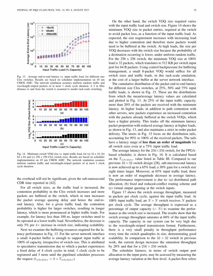
Next we examine the buffering resources required for the la-tency performance in Fig. 13. For the server network interfacea small 4-packet buffer is enough to support input traffic at100% of capacity, irrespective of switch size. This is attributedto speculative transmission due to which a packet experiencesa fixed delay of 4 clock cycles in total; 1 clock cycle to beregistered and 3 more until the pipelined scheduler processesthe request (tscheduler = 3× Tscheduler).
On the other hand, the switch VOQ size required varieswith the input traffic load and switch size. Figure 14 shows theminimum VOQ size in packet entries, required at the switchto avoid packet loss, as a function of the input traffic load. Asexpected, the size requirement increases with increasing loaddue to higher contention and therefore more packets wouldneed to be buffered at the switch. At high loads, the size perVOQ decreases with the switch size because the probability ofa destination occurring is lower, under uniform random traffic.For the 256 x 256 switch, the minimum VOQ size at 100%load is 32 packets, which translates to 512 KB per switch inputport for 64 B packets. Using control backpressure for bufferingmanagement, a small 8-packet VOQ would suffice for allswitch sizes and traffic loads, in this rack-scale emulation,at the cost of a larger buffer at the server network interface.
The cumulative distribution of the packet end-to-end latencyfor different size Clos switches, at 25%, 50% and 75% inputtraffic loads, is shown in Fig. 15. These are the distributionsfrom which the mean/average latency values are calculatedand plotted in Fig. 13. At 25% of the input traffic capacity,more than 20% of the packets are received with the minimumlatency. At higher loads, in addition to path contention withother servers, new packets experience an increased contentionwith the packets already buffered at the switch VOQs, whichhave a higher priority. This trades off the minimum latencypacket proportion with reduced average latency at higher loads,as shown in Fig. 13, and also maintains a strict in-order packetdelivery. The insets in Fig. 15 focus on the distribution tails,accounting for 99% to 100% of the received packets. The tailshave a latency range of less than an order of magnitude forall switch sizes even at a 75% input traffic load.
The average latency for the 256×256 switch, for the FPGA-based scheduler, is shown in Fig. 16. It is calculated basedon the Tscheduler value listed in Table III. Compared to ourprevious 32×32 switch design [28], sub-microsecond latencyis now achieved up to a 65% load; a 30% gain for a switch sizeeight times larger. Moreover, at 65% input traffic load, thereis now an order of magnitude decrease in average latency.The performance improvement is due to: (a) distributed pathallocation, (b) fixed and reduced-conflict routing scheme and(c) virtual output queuing at the switch inputs.
Figure 17 shows the switch average throughput, measuredin packets per clock cycle, against the input traffic load. At100% input traffic load, an N ×N switch receives N packetsper clock cycle. The average throughput is expressed as apercentage of output capacity (= N ) to examine the perfor-mance as the switch size is increased. The results show that theswitch average throughput saturates at 60% of the input trafficcapacity. The capacity in our system can be very high dueto the wavelength-striped transmission format. Furthermore,there is a very small penalty in throughput performanceevery time the switch quadruples in size, demonstrating goodscalability. In comparison to the 32 × 32 switch in previouswork, the current design increases the saturation throughputby 28% and that for a 256× 256 switch.
The scheduler fairness, in terms of switch output portallocation to the input ports, may be assessed by measuring theaverage latency variation at the flow-level. A packet flow refers
JOURNAL OF LATEX CLASS FILES, VOL. 14, NO. 8, AUGUST 2015 11
101
102
103
104
0
0.1
0.2
0.3
0.4
0.5
0.6
0.7
0.8
0.9
1
(a)
Cu
mu
lati
ve
Pro
ba
bil
ity
16x16
64x64
256x256
0 50 1000.99
1
101
102
103
104
0
0.1
0.2
0.3
0.4
0.5
0.6
0.7
0.8
0.9
1
(b)
Cu
mu
lati
ve
Pro
ba
bil
ity
0 500 1000 15000.99
1
101
102
103
104
Packet End-to-End Latency (ns)
0
0.1
0.2
0.3
0.4
0.5
0.6
0.7
0.8
0.9
1
(c)
Cu
mu
lati
ve
Pro
ba
bil
ity
0 4000 80000.99
1
Fig. 15. Cumulative distribution of the packet end-to-end latency at (a) 25%,(b) 50% and (c) 75% input traffic loads, for different size Clos switches.Results are based on scheduler implementation on 45 nm CMOS ASIC. Thenetwork emulation assumes uniform random traffic and wavelength-stripedpackets of at most 1 clock cycle duration. A 2 m fibre distance to and fromthe switch is assumed to model rack-scale switching.
to packets from one switch input port to the same output port.Therefore, in an N ×N switch, there are N flows per outputport. Figure 18 shows the standard deviation of the N flowaverage latencies, for each output port, at different input trafficloads. The standard deviation is shown increasing with switchsize and traffic load, indicating a decrease in fairness. Althoughround-robin arbitration is fair locally, at the system level thescheduler is less fair. In general, there is an inherent fairnesspenalty in distributed arbitration scheduling, where resourceaccess is decided for only a subset of requests. Furthermore,parallel-plane path allocation for new packets and higher-priority VOQ packets drops an increasing proportion of newpacket grants with traffic load, trading off fairness for strict
0 10 20 30 40 50 60 70 80 90 100
Input Traffic Load (% Capacity)
101
102
103
104
105
Avera
ge E
nd
-to
-En
d L
ate
ncy (
ns)
32x32, ECOC'17
256x256
Fig. 16. Average end-to-end latency vs. input traffic load, for different Closswitch schedulers. Results are based on scheduler implementation on theVirtex-7 XC7V690T FPGA board. The network emulation assumes uniformrandom traffic and wavelength-striped packets of at most 1 clock cycleduration. A 2 m fibre distance to and from the switch is assumed to modelrack-scale switching.
0 10 20 30 40 50 60 70 80 90 100
Input Traffic Load (% Capacity)
0
10
20
30
40
50
60
70
80
90
100
Sw
itch
Av
era
ge
Th
rou
gh
pu
t (%
Ca
pac
ity
)
16x16
64x64
256x256
32x32, ECOC'17
Fig. 17. Switch average throughput vs. input traffic load, for different sizeClos switches. Throughput is measured as the total number of packets perclock cycle across all output ports. Point-to-point connections are used as athroughput reference in a system with no contention.
in-order delivery and low average latency.
VII. CONCLUSION
We presented a highly-parallel and modular scheduler de-sign for optical Clos switches which are practical for scalablephotonic-integrated packet switching. A novel fixed path allo-cation scheme was used to completely eliminate contention atthe Clos central modules. For the input and output modules,allocation is distributed to dedicated scheduler modules toresolve any contention. The design for each scheduler hard-ware module has been optimized for clock speed, using aparallel and pipelined implementation, and was presented anddiscussed in detail.
Each hardware module in the scheduler was synthesizedas an ASIC in a 45 nm CMOS process. The implementa-tion results show that each module’s minimum clock periodscales sublinearly with the switch size, verifying scalability.Furthermore, for a 256 × 256 Clos switch, the minimumclock period for the entire scheduler unit is 2.0 ns, limitedby iSLIP allocation for the Clos input modules. This results
JOURNAL OF LATEX CLASS FILES, VOL. 14, NO. 8, AUGUST 2015 12
0 32 64 96 128 160 192 224 256
Output Port(a)
10-1
100
101
102
103
16x16
64x64
256x256
0 32 64 96 128 160 192 224 256
Output Port(b)
10-1
100
101
102
103
Standard Deviation of Average Flow Latency
0 32 64 96 128 160 192 224 256
Output Port(c)
10-1
100
101
102
103
Fig. 18. Standard deviation of the average flow latency per output port at (a) 25%, (b) 50% and (c) 75% input traffic loads, for different size Clos switches.Results are based on scheduler implementation on 45 nm CMOS ASIC. The network emulation assumes uniform random traffic and wavelength-stripedpackets of at most 1 clock cycle duration. A 2 m fibre distance to and from the switch is assumed to model rack-scale switching.
in a total scheduling delay of only 6.0 ns, in a 3-stage pipelinedimplementation of the scheduler, outperforming the fastestdesigns in the literature for the switch sizes considered here.
A cycle-accurate rack-scale emulation of our switch systemconcept was developed to measure the Clos switch perfor-mance under uniform random traffic. Based on the ASICimplementation results, the minimum end-to-end latency for a256×256 size is 32.0 ns, out of which only 6.0 ns are attributedto central scheduling. For this switch size, the average end-to-end latency remains on nanosecond time scales up to 80% ofinput traffic load. The distribution of the packet latency showsa short tail for all switch sizes examined, within an order ofmagnitude from the 99th percentile, even at a 75% load.
For implementation on the Xilinx Virtex-7 XC7V690TFPGA board, the 256-port switch average latency performanceremains on nanosecond timescale up to a 65% traffic load.Compared to a 32-port Clos switch in previous work, this is a30% load improvement for a switch size eight times larger. Theperformance gain is due to routing scheme, distributed pathallocation and virtual output queuing (VOQ) at the switch.
The switch achieves zero packet loss for all sizes up to100% of input traffic load. This is enabled by VOQ bufferingat the switch input ports. For the 256-port switch, the VOQsize requirement is 32 packets to avoid packet loss at fullport capacity, but can be as short as 8 packets long if controlbackpressure from the switch to the servers is applied.
The average throughput was also measured for all switchsizes and compared to previous work. The results showed thatthe switch saturates near 60% of port capacity with a verysmall penalty as the switch scales in size. For all sizes, theswitch maintains the peak throughput beyond saturation as theload is increased, indicating that the switch is stable. Moreover,compared to the 32-port Clos switch in previous work, thethroughput has now doubled for a switch size 8 times larger.
In distributed arbitration scheduling, resource allocationfairness is degraded as decisions are based only on a subsetof requests. In this work, scheduler fairness was assessedby examining the packet flow average latency from differentswitch input ports to the same output port. Our results showeda switch size and traffic load dependency on the fairnessdegradation. Future work will investigate scheduler designtechniques to mitigate this.
ACKNOWLEDGMENT
This work was supported by the UK Engineering andPhysical Sciences Research Council (EPSRC) under GrantEP/R035342/1 and in part by the EU Horizon 2020 programme(Industrial Leadership section) under Grant 687632.
REFERENCES
[1] Cisco Systems, Inc., “Cisco Global Cloud Index: Forecast and Method-ology, 2016 - 2021,” Cisco Systems, Inc., White Paper, 2018.
[2] G. Lee, Cloud Networking: Understanding Cloud-based Data CenterNetworks. Morgan Kaufmann, 2014.
[3] P. Goransson and C. Black, Software Defined Networks: A Comprehen-sive Approach. Morgan Kaufmann, 2014.
[4] N. Chrysos, F. Neeser, M. Gusat, C. Minkenberg, W. Denzel, C. Basso,M. Rudquist, K. M. Valk, and B. Vanderpool, “Large switches orblocking multi-stage networks? An evaluation of routing strategies fordatacenter fabrics,” Computer Networks, vol. 91, pp. 316 – 328, 2015.
[5] M. Alizadeh and T. Edsall, “On the data path performance of leaf-spinedatacenter fabrics,” in IEEE Hot Interconnects (HOTI), August 2013,pp. 71–74.
[6] Cisco Systems, Inc., “Cisco Nexus 3548 Switch Performance Valida-tion,” Cisco Systems, Inc., White Paper, December 2012.
[7] N. Zilberman, P. M. Watts, C. Rotsos, and A. W. Moore, “Reconfigurablenetwork systems and software-defined networking,” Proceedings of theIEEE, vol. 103, no. 7, pp. 1102–1124, July 2015.
[8] W. M. Mellette, R. McGuinness, A. Roy, A. Forencich, G. Papen, A. C.Snoeren, and G. Porter, “RotorNet: A scalable, low-complexity, opticaldatacenter network,” in Proceedings of the Conference of the ACMSpecial Interest Group on Data Communication, ser. SIGCOMM ’17.New York, NY, USA: ACM, 2017, pp. 267–280.
[9] G. Wang, D. G. Andersen, M. Kaminsky, K. Papagiannaki, T. E.Ng, M. Kozuch, and M. Ryan, “c-Through: Part-time optics in datacenters,” in Proceedings of the ACM SIGCOMM 2010 Conference, ser.SIGCOMM ’10. New York, NY, USA: ACM, 2010, pp. 327–338.
[10] N. Farrington, G. Porter, S. Radhakrishnan, H. H. Bazzaz, V. Subra-manya, Y. Fainman, G. Papen, and A. Vahdat, “Helios: A hybrid electri-cal/optical switch architecture for modular data centers,” in Proceedingsof the ACM SIGCOMM 2010 Conference, ser. SIGCOMM ’10. NewYork, NY, USA: ACM, 2010, pp. 339–350.
[11] A. Singla, A. Singh, K. Ramachandran, L. Xu, and Y. Zhang, “Proteus: Atopology malleable data center network,” in ACM SIGCOMM Workshopon Hot Topics in Networks (HotNets), ser. HotNets-IX. New York, NY,USA: ACM, 2010, pp. 1–6.
[12] G. Porter, R. Strong, N. Farrington, A. Forencich, P. Chen-Sun, T. Ros-ing, Y. Fainman, G. Papen, and A. Vahdat, “Integrating microsecondcircuit switching into the data center,” in Proceedings of the ACMSIGCOMM 2013 Conference, ser. SIGCOMM ’13. New York, NY,USA: ACM, 2013, pp. 447–458.
[13] Q. Cheng, L. Y. Dai, N. C. Abrams, Y.-H. Hung, P. E. Morrissey,M. Glick, P. O’Brien, and K. Bergman, “Ultralow-crosstalk, strictly non-blocking microring-based optical switch,” Photonics Research, vol. 7,no. 2, pp. 155–161, February 2019.
JOURNAL OF LATEX CLASS FILES, VOL. 14, NO. 8, AUGUST 2015 13
[14] P. DasMahapatra, R. Stabile, A. Rohit, and K. A. Williams, “Opticalcrosspoint matrix using broadband resonant switches,” IEEE Journal ofSelected Topics in Quantum Electronics, vol. 20, no. 4, pp. 1–10, July2014.
[15] N. Calabretta, W. Miao, K. Mekonnen, K. Prifti, and K. Williams,“Monolithically integrated WDM cross-connect switch for high-performance optical data center networks,” in Optical Fiber Commu-nications Conference and Exhibition (OFC), March 2017.
[16] Q. Cheng, A. Wonfor, J. Wei, R. V. Penty, and I. H. White, “Low-energy, high-performance lossless 8x8 SOA switch,” in Optical FiberCommunications Conference and Exhibition (OFC), March 2015.
[17] B. G. Lee, A. V. Rylyakov, W. M. J. Green, S. Assefa, C. W.Baks, R. Rimolo-Donadio, D. M. Kuchta, M. H. Khater, T. Barwicz,C. Reinholm, E. Kiewra, S. M. Shank, C. L. Schow, and Y. A. Vlasov,“Monolithic silicon integration of scaled photonic switch fabrics, CMOSlogic, and device driver circuits,” Journal of Lightwave Technology,vol. 32, no. 4, pp. 743–751, February 2014.
[18] N. Dupuis, F. Doany, R. A. Budd, L. Schares, C. W. Baks, D. M.Kuchta, T. Hirokawa, and B. G. Lee, “A nonblocking 4x4 Mach-Zehnderswitch with integrated gain and nanosecond-scale reconfiguration time,”in Optical Fiber Communication Conference (OFC), 2019.
[19] M. Ding, A. Wonfor, Q. Cheng, R. V. Penty, and I. H. White, “HybridMZI-SOA InGaAs/InP photonic integrated switches,” IEEE Journal ofSelected Topics in Quantum Electronics, vol. 24, no. 1, pp. 1–8, January2018.
[20] Z. Guo, L. Lu, L. Zhou, L. Shen, and J. Chen, “16x16 silicon op-tical switch based on dual-ring-assisted Mach-Zehnder interferometers,”Journal of Lightwave Technology, vol. 36, no. 2, pp. 225–232, January2018.
[21] Q. Yang, K. Bergman, G. D. Hughes, and F. G. Johnson, “WDMpacket routing for high-capacity data networks,” Journal of LightwaveTechnology, vol. 19, no. 10, pp. 1420–1426, October 2001.
[22] A. Shacham and K. Bergman, “Building ultralow-latency interconnec-tion networks using photonic integration,” IEEE Micro, vol. 27, no. 4,pp. 6–20, July 2007.
[23] R. Luijten, C. Minkenberg, R. Hemenway, M. Sauer, and R. Grzybowski,“Viable opto-electronic HPC interconnect fabrics,” in ACM/IEEE Super-computing Conference, Nov 2005.
[24] R. Proietti, C. J. Nitta, Y. Yin, R. Yu, S. J. B. Yoo, and V. Akella,“Scalable and distributed contention resolution in AWGR-based datacenter switches using RSOA-based optical mutual exclusion,” IEEEJournal of Selected Topics in Quantum Electronics, vol. 19, no. 2, pp.3 600 111–3 600 111, March 2013.
[25] I. Cerutti, J. A. Corvera, S. M. Dumlao, R. Reyes, P. Castoldi, andN. Andriolli, “Simulation and FPGA-based implementation of iterativeparallel schedulers for optical interconnection networks,” Journal ofOptical Communications and Networking, vol. 9, no. 4, pp. C76–C87,April 2017.
[26] P. Andreades, Y. Wang, J. Shen, S. Liu, and P. M. Watts, “Experimentaldemonstration of 75 ns end-to-end latency in an optical top-of-rackswitch,” in Optical Fiber Communications Conference and Exhibition(OFC), March 2015.
[27] P. Andreades, K. Clark, P. M. Watts, and G. Zervas, “Experimentaldemonstration of an ultra-low latency control plane for optical packetswitching in data center networks,” Optical Switching and Networking,vol. 32, pp. 51–60, November 2019.
[28] P. Andreades and P. M. Watts, “Low latency parallel schedulers forphotonic integrated optical switch architectures in data centre networks,”in European Conference on Optical Communication (ECOC), September2017.
[29] P. Andreades and G. Zervas, “Parallel distributed schedulers for scalablephotonic integrated packet switching,” in Photonics in Switching andComputing (PSC), September 2018.
[30] C. Clos, “A study of non-blocking switching networks,” The Bell SystemTechnical Journal, vol. 32, no. 2, pp. 406–424, March 1953.
[31] I. H. White, E. T. Aw, K. A. Williams, H. Wang, A. Wonfor, and R. V.Penty, “Scalable optical switches for computing applications [Invited],”Journal of Optical Networking, vol. 8, no. 2, pp. 215–224, Feb 2009.
[32] A. Shacham, B. A. Small, O. Liboiron-Ladouceur, J. P. Mack, andK. Bergman, “An ultra-low latency routing node for optical packetinterconnection networks,” in IEEE Lasers and Electro-Optics Society(LEOS), vol. 2, November 2004, pp. 565–566.
[33] A. Shacham, B. G. Lee, and K. Bergman, “A wide-band nonblocking2x2 switching node for a SPINet network,” IEEE Photonics TechnologyLetters, vol. 17, no. 12, pp. 2742–2744, December 2005.
[34] J. Luo, S. Di Lucente, J. Ramirez, H. J. S. Dorren, and N. Cal-abretta, “Low latency and large port count optical packet switch with
highly distributed control,” in Optical Fiber Communication Conferenceand Exposition and the National Fiber Optic Engineers Conference(OFC/NFOEC), March 2012.
[35] F. Yan, W. Miao, O. Raz, and N. Calabretta, “OPSquare: A flat DCNarchitecture based on flow-controlled optical packet switches,” Journalof Optical Communications and Networking, vol. 9, no. 4, pp. 291–303,April 2017.
[36] W. Miao, J. Luo, S. Di Lucente, H. Dorren, and N. Calabretta, “Novel flatdatacenter network architecture based on scalable and flow-controlledoptical switch system,” Optics Express, vol. 22, no. 3, pp. 2465–2472,February 2014.
[37] X. Zheng, D. Patil, J. Lexau, F. Liu, G. Li, H. Thacker, Y. Luo,I. Shubin, J. Li, J. Yao, P. Dong, D. Feng, M. Asghari, T. Pinguet,A. Mekis, P. Amberg, M. Dayringer, J. Gainsley, H. F. Moghadam,E. Alon, K. Raj, R. Ho, J. E. Cunningham, and A. V. Krishnamoorthy,“Ultra-efficient 10Gb/s hybrid integrated silicon photonic transmitter andreceiver,” Optics Express, vol. 19, no. 6, pp. 5172–5186, March 2011.
[38] W. J. Dally and B. P. Towles, Principles and Practices of InterconnectionNetworks. Elsevier, 2004.
[39] P. Gupta and N. McKeown, “Designing and implementing a fast crossbarscheduler,” IEEE Micro, vol. 19, no. 1, pp. 20–28, January 1999.
[40] N. McKeown, “The iSLIP scheduling algorithm for input-queuedswitches,” IEEE/ACM Transactions on Networking, vol. 7, no. 2, pp.188–201, April 1999.
[41] R. C. Figueiredo, N. S. Ribeiro, A. M. O. Ribeiro, C. M. Gallep,and E. Conforti, “Hundred-picoseconds electro-optical switching withsemiconductor optical amplifiers using multi-impulse step injectioncurrent,” Journal of Lightwave Technology, vol. 33, no. 1, pp. 69–77,January 2015.
[42] K. Clark, H. Ballani, P. Bayvel, D. Cletheroe, T. Gerard, I. Haller,K. Jozwik, K. Shi, B. Thomsen, P. Watts, H. Williams, G. Zervas,P. Costa, and Z. Liu, “Sub-nanosecond clock and data recovery in anoptically-switched data centre network,” in European Conference onOptical Communication (ECOC), September 2018.