ww ww ww iopscience.org/jmm ISSN 0960-1317 Journal of Micromechanics an d Microengineering St ructures, devices and systems Journal of Micromechanics and Microengineering Vol 21, No 11 115001–115033 November 2011 Volume 21 Number 11 November 2011
Transcript
ww
Journal of Micromechanicsand Microengineering
ww ww
iopscience.org/jmm
ISSN 0960-1317
Journal of Micromechanicsand Microengineering Structures, devices and systemsPAPERS
115001 Integrated nanohole array surface plasmon resonance sensing device using a dual-wavelength sourceC Escobedo, S Vincent, A I K Choudhury, J Campbell, A G Brolo, D Sinton and R Gordon
115002 Microthermoforming of microfluidic substrates by soft lithography (µTSL): optimization using design ofexperimentsM Focke, D Kosse, D Al-Bamerni, S Lutz, C Muller, H Reinecke, R Zengerle and F von Stetten
115003 Self-aligned mask renewal for anisotropically etched circular micro- and nanostructuresPeter Kaspar, Sebastian Holzapfel, Erich J Windhab and Heinz Jackel
115004 Improving the height of replication in EHD patterning by optimizing the electrical properties of thetemplateXin Li, Jinyou Shao, Yucheng Ding, Hongmiao Tian and Hongzhong Liu
115005 Development of individually-addressable parylene microtube arraysYuefa Li, Hongen Tu, Raymond Iezzi, Paul Finlayson and Yong Xu
115006 Visualization of turbulent reactive mixing in a planar microscale confined impinging-jet reactorYanxiang Shi, Vishwanath Somashekar, Rodney O Fox and Michael G Olsen
115007 An analytical model and verification for MEMS Pirani gaugesF Santagata, E Iervolino, L Mele, A W van Herwaarden, J F Creemer and P M Sarro
115008 Controlled deposition of sol–gel sensor material using hemiwickingMorten Bo Mikkelsen, Rodolphe Marie, Jan H Hansen, Dorota Wencel, Colette McDonagh, Hans Ole Nielsenand Anders Kristensen
115009 Modeling, fabrication and demonstration of a rib-type cantilever switch with an extended gate electrodeMin-Wu Kim, Yong-Ha Song and Jun-Bo Yoon
115010 Photolithographic structuring of stretchable conductors and sub-kPa pressure sensorsC L Tuinea-Bobe, P Lemoine, M U Manzoor, M Tweedie, R A D’sa, C Gehin and E Wallace
115011 The effect of meniscus on the permeability of micro-post arraysChan Byon and Sung Jin Kim
115012 Development of patterned carbon nanotubes on a 3D polymer substrate for the flexible tactile sensorapplicationChih-Fan Hu, Wang-Shen Su and Weileun Fang
115013 Polymerization shrinkage stress measurement for a UV-curable resist in nanoimprint lithographyAlborz Amirsadeghi, Jae Jong Lee and Sunggook Park
115014 Rapid nano impact printing of silk biopolymer thin filmsRobert D White, Caprice Gray, Ethan Mandelup, Jason J Amsden, David L Kaplan and Fiorenzo G Omenetto
115015 Silicon-based bridge wire micro-chip initiators for bismuth oxide–aluminum nanothermiteC S Staley, C J Morris, R Thiruvengadathan, S J Apperson, K Gangopadhyay and S Gangopadhyay
115016 A dynamic model of valveless micropumps with a fluid damping effectT X Dinh and Y Ogami
115017 Novel temperature compensation technique for force-sensing piezoresistive devicesJoshua Scott and Eniko T Enikov
115018 Highly sensitive ZnO thin film bulk acoustic resonator for hydrogen detectionDa Chen, Jing-jing Wang, Qi-xin Liu, Yan Xu, De-hua Li and Yi-jian Liu
Received 7 June 2011, in final form 10 September 2011Published 14 October 2011Online at stacks.iop.org/JMM/21/115021
AbstractWe present a design methodology and manufacturing process for the construction ofarticulated three-dimensional microstructures with features on the micron to centimeter scale.Flexure mechanisms and assembly folds result from the bulk machining and lamination ofalternating rigid and compliant layers, similar to rigid-flex printed circuit board construction.Pop-up books and other forms of paper engineering inspire designs consisting of one complexpart with a single assembly degree of freedom. Like an unopened pop-up book, mechanismlinks reside on multiple interconnected layers, reducing interference and allowing foldingmechanisms of greater complexity than achievable with a single folding layer. Machined layersare aligned using dowel pins and bonded in parallel. Using mechanical alignment that persistsduring bonding allows device layers to be anisotropically pre-strained, a feature we exploit tocreate self-assembling structures. These methods and three example devices are presented.
1. Introduction
Many machines realize greater performance and economyif made smaller. However, when shrunk to millimeter andmicron sizes, new challenges arise in their construction.Monolithic fabrication must replace traditional methods,enabling efficient batch processing while eliminating theonerous assembly and handling of individual components.Integrated circuit technology has strongly influenced andinformed this monolithic approach. Fabrication techniquesinclude optical lithography, physical and chemical vapordeposition, spin coating of polymers, electroplating, thermaltreatment, chemical and plasma etching, abrasive polishingand laser machining. Micro-devices with a variety of electricaland mechanical functions manufactured using these (andother) techniques are named microelectromechanical systems(MEMS). Many MEMS devices have found wide commercialsuccess, including miniaturized accelerometers, gyroscopes,displays, electrical and optical switches, scanning mirrorsand pressure sensors [1]. The success of these devices isdue not only to the increased performance and reduced costsassociated with miniaturization and batch fabrication, butto their tolerance of the limitations imposed by monolithicfabrication using integrated circuit techniques.
Most MEMS devices are made using surfacemicromachining [2]. Material is deposited onto a substrate,masked and then etched. These steps are repeated to buildup layers. As most methods of deposition are isotropic,chemical–mechanical polishing is often used to planarize eachlayer. Free-standing mechanical structures are created by
removing sacrificial material or etching undercuts. Whenmultiple materials are used, earlier layers must survive laterdeposition, etching and thermal treatment steps, potentiallylimiting the combinations of materials that can be used.Complex MEMS devices may have several material layersand require hundreds of sequential process steps. This highlyserial nature compounds the impact of defects introduced ateach step. To achieve economical device yields, it is thennecessary to reduce the number of layers and shrink the size ofthe individual devices. Most commercially successful MEMSdevices are not hindered by a restriction to planar structures,material limitations or increasing miniaturization. Indeed,many of the devices previously listed consist of a siliconstructural element oscillating at high speed along a singleaxis. These requirements are well met by tiny, planar siliconcomponents. Silicon has excellent specific stiffness and lowthermal distortion, and processing methods therefore are welldeveloped [3].
There is strong interest in constructing non-planarminiature devices that do not conform to traditionalMEMS processing. These devices—which include motors,transmissions, linkages, linear and rotary servo elements,micro-robots and complex three-dimensional structures—arechallenging to create using surface micromachining. There arepractical limitations on the types and thicknesses of materialthat can be deposited by vapor deposition, spin coating andelectroplating. It is not practical to use more than a few devicelayers, but within these restrictions, surface-machined gears,motors and other mechanical devices have been made [4].Bulk machining—a technique in which multiple substrates
J. Micromech. Microeng. 21 (2011) 115021 J P Whitney et al
are machined separately and then bonded together—is analternative MEMS process which eliminates the need forsequential planarization and allows layer substrates to beprocessed in parallel. Bulk machining enables thicker layersand allows for a wider range of layer materials. It has been usedto create a variety of structurally complex miniature devices,including gas turbines [5], multi-axis force sensors [6] andmicrofluidic devices [7].
To overcome planar limitations inherent to MEMS, therehas been much effort to create three-dimensional structuresthrough folding. Surface-machined pin-and-staple hinges [8]and polymer flexures [9] are two common methods used tocreate folding linkages. Schemes to exploit deposition stresses[10] or solder/polymer surface tension during reflow [11] arecommon ways to induce folding. Co-fabricated assemblyactuators [12], though bulky, allow for a highly controlledfold sequence. If latching mechanisms are present, stochasticassembly through simple agitation might also be used.
2. Design and fabrication methods
In this paper, we present a new method for making three-dimensional MEMS devices and microstructures, based onthe folding of multilayer rigid-flex laminates. Essentially, weare combining the surface-machining methods of folding andself-assembly with the simplicity and material flexibility ofbulk machining. These ideas have been strongly influenced byprinted circuit board (PCB) fabrication. In particular, we haveadopted adhesive bonding, mechanical layer alignment andparallel lamination—all common PCB fabrication methods.
2.1. Printed circuit board techniques
Bulk-machined multilayer MEMS devices are constructed bymachining individual layers (typically using deep reactive ionetching or chemical wet etching), followed by lamination usingwafer bonding. Alignment accuracy of 1–5 μm is typicalfor direct bonding methods, although successive bonding ina multilayer device leads to accumulated error. For methodsthat use an intermediate bonding material, such as adhesive,glass frit, eutectic or solder bonding, alignment accuracyis degraded by flow and thermal expansion of the bondingagent. There has been effort to integrate mechanical alignmentfeatures into layer substrates (typically silicon wafers) toprevent them from shifting during the bonding cycle. Surface-machined aluminum disks were used as friction pads toimprove post-bond alignment by an order of magnitude forbenzocyclobutene adhesive bonding [13]. Bulk-machinedpost-and-trench alignment features have also been used, notonly to improve alignment, but to achieve it by mechanical,rather than optical means [14]. Adoption of PCB alignmentand bonding techniques is a natural extension of these efforts.
Multilayer PCBs use precision dowel pins to maintainalignment during lamination. Alignment holes are punched orlaser-drilled in each layer. The laminate is placed betweenprecision die plates with relief holes for the alignmentpins and then bonded in a heated press. Multiple layersare easily aligned and bonded simultaneously. Since
mechanical alignment persists throughout the bonding cycle,misalignment from adhesive shearing and layer migration islargely eliminated. The challenges of achieving high bondstrength, low adhesive flow and high accuracy alignmentare well understood, and a wide array of highly optimizedmaterials, tools and techniques are commercially available tosupport high-accuracy parallel lamination.
2.2. Laminate fabrication
Our process begins with the production of multilayerlaminates. Individual layers are first bulk machined todefine part geometry. Layers—post machining—must remaincontiguous to preserve structural integrity of the layer andprovide a stable mechanical connection from each devicecomponent to the alignment pins. Usual practice is to machinefeatures while leaving small tabs or ‘bridges’ connecting partsto the surrounding bulk material, similar to break-off tabs inpanelized circuit boards. After lamination, a second roundof machining, the ‘singulation’ step, will free the individualparts. Any method of machining that is sufficiently accurateand compatible with the layer materials can be used. For ourresearch purposes, we use laser micromachining for its mask-less nature and compatibility with a wide range of materials.We employ a diode-pumped Nd:YVO4 laser, q-switched andfrequency tripled to 355 nm. Maximum average power is1.5 W, which we find sufficient for machining layers in the1–150 μm thickness range. The beam is focused to a spotapproximately 8 μm in diameter using a telecentric objectivelens. Full-range accuracy and repeatability of beam/partpositioning is 2 μm or better. With this system, adhesive andpolymer layers for all devices presented took a few seconds tomachine, and metal and carbon fiber layers took a few minuteseach. Layers were 25–50 mm in size.
After each layer is machined, optional steps—such aselectropolishing, ultrasonic cleaning and plasma treatment—may be performed to prepare each layer for lamination. Inflex circuit construction, circuit layers are usually bondedwith acrylic sheet adhesives. PCB sheet adhesives arehighly engineered materials with tailored thermal expansionproperties, and they exhibit very little flow during the bondingcycle. We use Dupont FR1500, a commercially-availableacrylic sheet adhesive, 12.5 μm thick. The adhesive is usedin two ways: it is either machined with alignment holesand included as a free-standing layer, or it is tack-bondedto an adjacent layer. For either technique, laser machining isused to pattern the adhesive. Other adhesives or methods ofadhesion could certainly be used, but we find the combinationof properties present in this type to be suitable for our purposes.
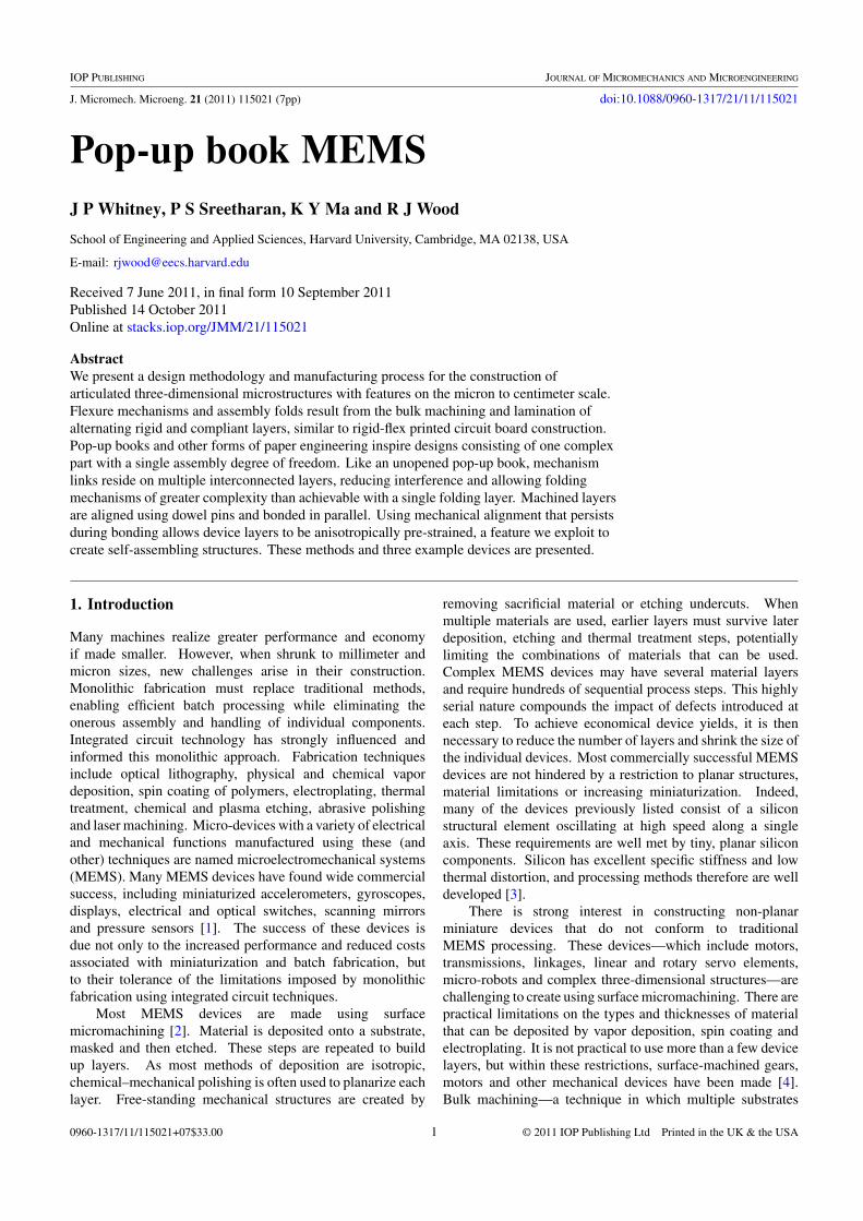
Figure 1 illustrates the alignment tooling used duringlamination. This alignment and bonding configuration istypical of PCB lamination. After stacking the layers, thelayup and tooling are placed in a heated press for bonding. Thetypical lamination cycle used was 1 h at 190◦C with 400 kPa ofpressure. Alignment accuracy is determined by several factors:alignment hole and pin accuracy, coefficients of thermalexpansion for each layer material, bonding temperature andthe laminate dimensions. For alignment, we use precision
2
J. Micromech. Microeng. 21 (2011) 115021 J P Whitney et al
Figure 1. Exploded view of the alignment tooling used to align andbond multiple layers in parallel. Release/conformal layers, shown inred, sandwich the part layers. After stacking layers onto thealignment pins, the part and tooling are placed in a heated press forbonding.
dowel pins (1/16in); layer material permitting, alignment holesare undersized by a few microns to exploit elastic averaging.In practice, post-lamination alignment is better than 5 μm.The exact accuracy is difficult to measure since the materialuniformity and edge roughness of our current materials andmachining process are of a similar scale.
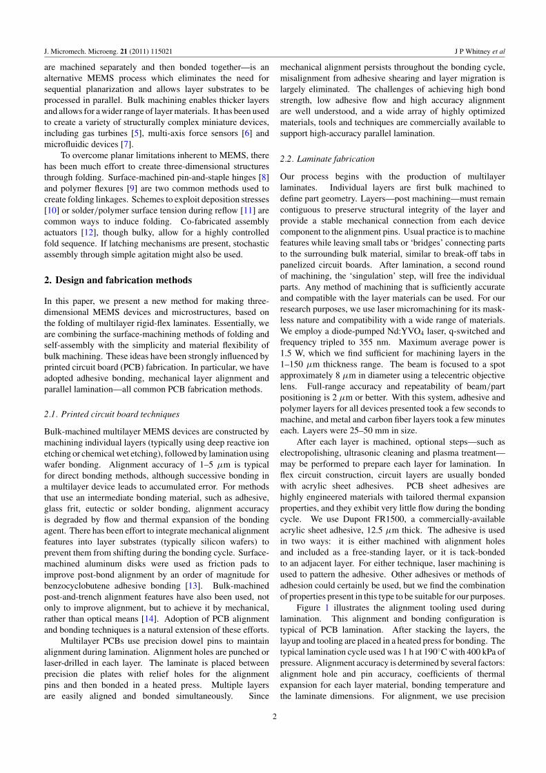
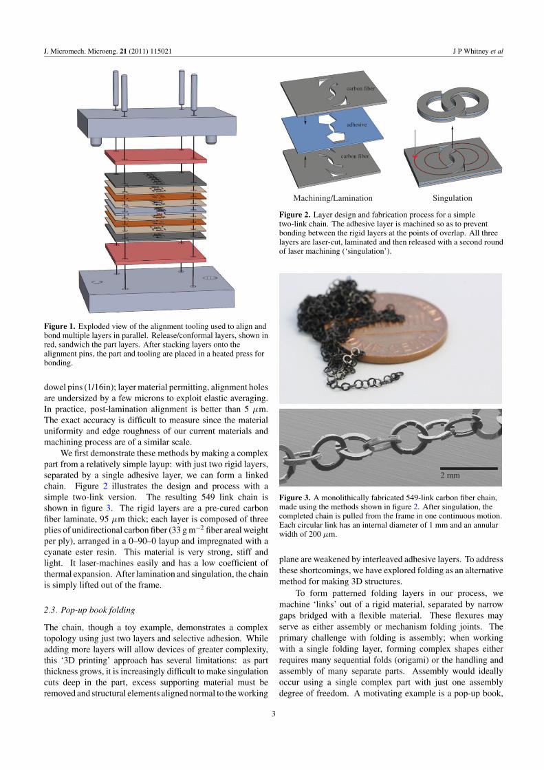
We first demonstrate these methods by making a complexpart from a relatively simple layup: with just two rigid layers,separated by a single adhesive layer, we can form a linkedchain. Figure 2 illustrates the design and process with asimple two-link version. The resulting 549 link chain isshown in figure 3. The rigid layers are a pre-cured carbonfiber laminate, 95 μm thick; each layer is composed of threeplies of unidirectional carbon fiber (33 g m−2 fiber areal weightper ply), arranged in a 0–90–0 layup and impregnated with acyanate ester resin. This material is very strong, stiff andlight. It laser-machines easily and has a low coefficient ofthermal expansion. After lamination and singulation, the chainis simply lifted out of the frame.
2.3. Pop-up book folding
The chain, though a toy example, demonstrates a complextopology using just two layers and selective adhesion. Whileadding more layers will allow devices of greater complexity,this ‘3D printing’ approach has several limitations: as partthickness grows, it is increasingly difficult to make singulationcuts deep in the part, excess supporting material must beremoved and structural elements aligned normal to the working
carbon fiber
carbon fiber
adhesive
Machining/Lamination Singulation
Figure 2. Layer design and fabrication process for a simpletwo-link chain. The adhesive layer is machined so as to preventbonding between the rigid layers at the points of overlap. All threelayers are laser-cut, laminated and then released with a second roundof laser machining (‘singulation’).
2 mm
Figure 3. A monolithically fabricated 549-link carbon fiber chain,made using the methods shown in figure 2. After singulation, thecompleted chain is pulled from the frame in one continuous motion.Each circular link has an internal diameter of 1 mm and an annularwidth of 200 μm.
plane are weakened by interleaved adhesive layers. To addressthese shortcomings, we have explored folding as an alternativemethod for making 3D structures.
To form patterned folding layers in our process, wemachine ‘links’ out of a rigid material, separated by narrowgaps bridged with a flexible material. These flexures mayserve as either assembly or mechanism folding joints. Theprimary challenge with folding is assembly; when workingwith a single folding layer, forming complex shapes eitherrequires many sequential folds (origami) or the handling andassembly of many separate parts. Assembly would ideallyoccur using a single complex part with just one assemblydegree of freedom. A motivating example is a pop-up book,
3
J. Micromech. Microeng. 21 (2011) 115021 J P Whitney et al
A
A
Section A-A
21
access port
bridge
3456789101112131415
ACF
CFAPIACFACFAPIACFACF
Laminate Index Layer CF 3 Laser Toolpath
Figure 4. The model Wright Flyer is made of 95 μm carbon fiber laminate (CF), Dupont FR1500 sheet adhesive (A) and 7.5 μm polyimidefilm (PI). Examples of bridge and access port features are shown on layer CF 3. The folding mechanism for the front and rear stabilizers issimilar to the wing box/fuselage mechanism shown. After lamination, the lower wings are opened like a book.
2 mm
Figure 5. Top: 1:900 scale 1903 Wright Flyer model afterlamination and singulation. All layers are bonded in a singlelamination cycle. Bottom: the model after folding, held withtweezers above a US quarter. The wing span is 14 mm, the wingsare separated by 2 mm and the vertical wing spars are 100 μm ×100 μm in cross section.
where a single rotation results in the folding and assembly ofmany interconnected components.
Using our laminated fabrication process, we can make‘pop-up book’ structures monolithically; multiple rigid-flexfolding layers are stacked and selectively bonded together.Four-bar linkages, spatial linkages and other complex closed-loop mechanisms can be formed without assembly, an ideapreviously explored in surface-machined MEMS [15]. Asa demonstration, we constructed a miniature model of the1903 Wright Flyer, at 1:900 scale. As shown in figure 4, thismodel consists of 15 physical layers: 6 rigid layers (carbon
mµ 005mm 2
100 µm
A
B
A
B
Figure 6. Electron micrographs of layer CF 3 after laser-cutting,ultrasonic cleaning and tack bonding and patterning of adhesivelayer A 4 (shown in blue false color).
fiber, as before), 7 adhesive layers (Dupont FR1500) and 2polymer flexure layers (7.5 μm polyimide film) which areshared by adjacent rigid layers to form 4 rigid-flex foldinglayers. The folding layers are connected together to forma series of parallel four-bar linkages. Figure 4 also showsthe laser tool path for a rigid layer (CF 3) and a portion offolding mechanism employed. After the layers are laser-cutand laminated, the model is released by trimming each bridgeconnecting linkage elements to the bulk material. Bridges onlower layers are exposed by ‘access ports’ on layers above.After releasing the model, assembly proceeds in a singlemotion by opening the wings like a book. Figure 5 showsthe Wright Flyer before and after folding. A small under-wingbrace and cyanoacrylate adhesive were manually applied to fixthe model in its folded state.
To create complex multi-layer folding mechanisms,small patches of adhesive form ‘mechanical vias’ connectingadjacent layers, analogous to electrical vias connecting
4
J. Micromech. Microeng. 21 (2011) 115021 J P Whitney et al
conductive layers in PCBs. Requiring a contiguous free-standing adhesive layer to make these connections can bean onerous restriction; if the adhesive layer is free standing,bridges of adhesive must connect each via patch, but thesebridges lead to large areas of unwanted bonding betweenfolding layers. To mitigate this problem, we employ one of twomethods to ‘tack bond’ adhesive patches to neighboring rigidlayers. In the first method, sheet adhesive is tacked (using lowheat and pressure) to a pre-machined rigid layer. The adhesiveis then laser-skived, leaving the required patches. In the secondmethod, sheet adhesive is kiss-cut at low laser power whilestill on its release paper backing. Alignment holes are thenmachined into the backing, allowing mechanical alignmentwhen the adhesive is transferred to an adjacent rigid layer bytack bonding. Figure 6 shows rigid layer CF 3 of the modelafter initial laser machining and ultrasonic cleaning. Adhesivelayer A 4 has been tack bonded to the top surface and thenpatterned; the remaining adhesive is shown false colored inblue.
While inter-layer alignment was consistently within 5 μm,comfortably below the minimum feature size for the device,occasional yield losses resulted from material defects. Fibergaps, such as those visible in figure 6, can ruin a part if theyoverlap critical bonding regions. While rejected parts due tomaterial defects were not common, the assembly step provedtricky. Assembly of this part does truly consist of a singlerotational fold, but grasping and handling the device withtweezers is a delicate operation. The miniature flexures areeasily torn with a small slip or tremor of the hand. Customizedassembly jigs would certainly make this process easier, buttheir use dilutes the advantages of a monolithic structure. Ifpractical devices are to be successfully mass-produced, theymust interface with simple external assembly actuators or theymust include a mechanism for self-assembly.
2.4. Self-assembly
When dealing with miniature, batch-fabricated devices, self-assembly is highly desired, but rather difficult to arrange. Inthe absence of external manipulation or energy input, assemblywill only proceed spontaneously if the laminate is not atits minimum energy state when released. To establish thiscondition in our laminates, we can introduce a pre-strainedelastic layer; in particular, we use common spring steelshim-stock, laser-cut into flat springs. Materials used forsprings must have a high yield strain, high toughness andmust not anneal during the bonding step. This spring-patternlayer is stretched and held under tension during bonding.Persistent mechanical alignment is critical to establishingand maintaining accurate anisotropic pre-strain within thelaminate.
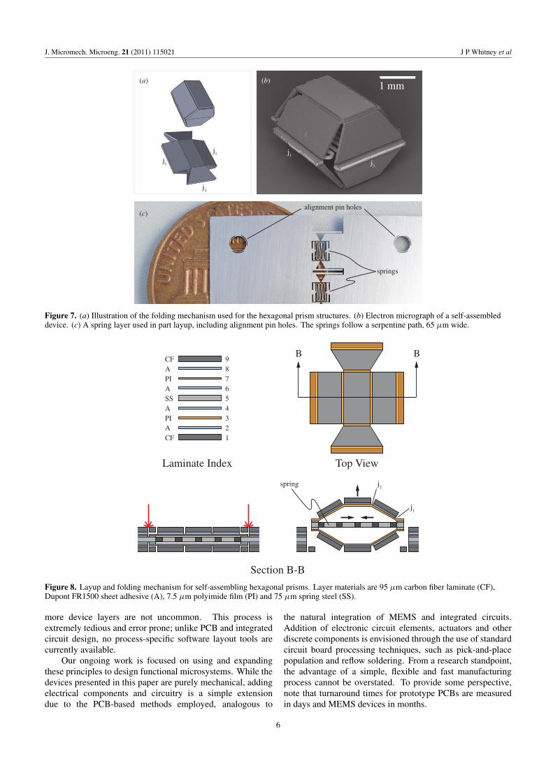
As a demonstration, we created self-assemblinghexagonal prisms. Our method and demonstration structureare partially inspired by previous work in recreational paperengineering which achieved spontaneous folding using pre-stretched rubber bands [16]. Figure 7(a) illustrates thestructure and its folding mechanism; the hexagonal ends arebisected, allowing the device to flatten, effectively creating a
one degree-of-freedom Sarrus linkage. Opposing fold joints,labelled j1, are connected by a flat spring. Figure 8 showsthe part layup and illustrates the folding mechanism. Layupmaterials are the same as those in the chain and Wright Flyerexamples, with the addition of a 75 μm spring steel layer.The alignment holes for this layer are shifted inward along thespring axis; the layer must be stretched to fit onto the alignmentpins.
After lamination, the ends of the springs are laser-cut, releasing the parts. However, this particular device islaminated into a singular configuration, since the j1 and j2hinges are co-planar. To initiate assembly, the structureswere dipped into an ultrasonically agitated water bath. They‘popped up’ into form immediately. The design could bemodified to move the j2 hinges outward with respect to thecentral layer, resulting in immediate buckling and assemblyafter spring release. The disadvantage of such a design is thepotential for premature release of one spring end during therelease cut.
This structure demonstrates the viability of self-assemblyusing a pre-strained layer. Many practical devices will requirehigh-accuracy assembly folds. We expect this can be achievedthrough kinematic fold stops and a spring layer designed toprovide positive closing action after assembly. In addition toa positive-acting spring, ‘snap-fit’ latches might be employedto prevent unfolding of the device.
3. Discussion and future work
These techniques cannot easily compete with surfacemicromachining in terms of layer thinness and featureresolution. As a bulk-machined process, these properties arelimited by handling and stability requirement for each layerand characteristics of the adhesive method used. The methodspresented in this paper hold promise for devices at a scalejust above traditional surface-micromachined devices, andMEMS devices which require complex mechanical structuresor specialized materials.
Using standard PCB processing facilities will requirepre-machining of device layers or the availability of on-site laser machining or other systems appropriate for bulkmachining. While the type of laser used in this workis commercially employed for laser-drilling electrical vias(especially in high-density flex circuits), they would needto be configured for machining and singulation as well.Achieving the degree of accuracy reported here will requirespecial attention to panel size (thermal effects) and the layoutdensity of alignment pins. Larger devices with tolerancesin line with current PCB practices can be produced withoutmodification. As circuit traces and material thicknessesshrink below 25 μm, and advanced packaging techniquesproliferate, commercial production will become morepractical.
Some aspects of paper engineering, such as a pop-up bookdesign, have provided a source of initial folding strategiesfor monolithic devices; however, general design principlesfor folding and assembly of these structures have not beenestablished. Our designs are currently hand-drafted—20 or
5
J. Micromech. Microeng. 21 (2011) 115021 J P Whitney et al
1 mm(a)
(c)
(b)
j1
j1 j
3
j3
j1
springs
alignment pin holes
Figure 7. (a) Illustration of the folding mechanism used for the hexagonal prism structures. (b) Electron micrograph of a self-assembleddevice. (c) A spring layer used in part layup, including alignment pin holes. The springs follow a serpentine path, 65 μm wide.
BB
Section B-B
spring
Top View
21
3456789
ACF
PIASSAPIACF
Laminate Index
j1
j2
Figure 8. Layup and folding mechanism for self-assembling hexagonal prisms. Layer materials are 95 μm carbon fiber laminate (CF),Dupont FR1500 sheet adhesive (A), 7.5 μm polyimide film (PI) and 75 μm spring steel (SS).
more device layers are not uncommon. This process isextremely tedious and error prone; unlike PCB and integratedcircuit design, no process-specific software layout tools arecurrently available.
Our ongoing work is focused on using and expandingthese principles to design functional microsystems. While thedevices presented in this paper are purely mechanical, addingelectrical components and circuitry is a simple extensiondue to the PCB-based methods employed, analogous to
the natural integration of MEMS and integrated circuits.Addition of electronic circuit elements, actuators and otherdiscrete components is envisioned through the use of standardcircuit board processing techniques, such as pick-and-placepopulation and reflow soldering. From a research standpoint,the advantage of a simple, flexible and fast manufacturingprocess cannot be overstated. To provide some perspective,note that turnaround times for prototype PCBs are measuredin days and MEMS devices in months.
6
J. Micromech. Microeng. 21 (2011) 115021 J P Whitney et al
Acknowledgments
The authors thank Dr James Weaver for providing the SEMimages. This work was supported in part by the ArmyResearch Laboratory (award number W911NF-08-2-0004)and the Wyss Institute for Biologically Inspired Engineering.
References
[1] Judy J W 2001 Microelectromechanical systems (MEMS):fabrication, design and applications Smart Mater. Struct.10 1115–34
[2] Bustillo J M, Howe R T and Muller R S 1998 Surfacemicromachining for microelectromechanical systems Proc.IEEE 86 1552–74
[3] Petersen K E 1982 Silicon as a mechanical material Proc.IEEE 70 420–57
[4] Mehregany M, Gabriel K J and Trimmer W S N 1988Integrated fabrication of polysilicon mechanisms IEEETrans. Electron. Devices 35 719–23
[5] Frechette L G, Jacobson S A, Breuer K S, Ehrich F F, GhodssiR, Khanna R, Wong C W, Zhang X, Schmidt M Aand Epstein A H 2005 High-speed microfabricated siliconturbomachinery and fluid film bearingsJ. Microelectromech. Syst. 14 141–52
[6] Beyeler F, Muntwyler S and Nelson B J 2009 A six-axisMEMS forcetorque sensor with micro-newton andnano-newtonmeter resolution J. Microelectromech. Syst.18 433–41
[7] Agirregabiria M, Blanco F J, Berganzo J, Arroyo M T,Fullaondo A, Mayora K and Ruano-Lopez J M 2005
Fabrication of SU-8 multilayer microstructures based onsuccessive CMOS compatible adhesive bonding andreleasing steps Lab Chip 5 545–52
[8] Pister K S J, Judy M W, Burgett S R and Fearing R S1992 Microfabricated hinges Sensors ActuatorsA 33 249–56
[9] Suzuki K, Shimoyama I, Miura H and Ezura Y 1992 Creationof an insect-based microrobot with an external skeleton andelastic joints Proc. Micro Electro Mechanical Systems(Travemunde, Germany) pp 190–5
[10] Arora W J, Nichol A J, Smith H I and Barbastathis G2006 Membrane folding to achieve three-dimensionalnanostructures: nanopatterned silicon nitridefolded with stressed chromium hinges Appl. Phys. Lett.88 053108
[11] Syms R R A, Yeatman E M, Bright V M and Whitesides G M2003 Surface tension-powered self-assembly ofmicrostructures—the state-of-the-art J. Microelectromech.Syst. 12 387–417
[12] Reid J R, Bright V M and Butler J T 1998 Automatedassembly of flip-up micromirrors Sensors ActuatorsA 66 292–8
[13] Niklaus F, Enoksson P, Kalvesten E and Stemme G 2003 Amethod to maintain wafer alignment precision duringadhesive wafer bonding Sensors Actuators A 107 273–8
[14] Slocum A H and Weber A C 2003 Precision passivemechanical alignment of wafers J. Microelectromech. Syst.12 826–34
[15] Hui E E, Howe R T and Rodgers M S 2000 Single-stepassembly of complex 3-D microstructures Proc. MicroElectro Mechanical Systems (Miyazaki, Japan) pp 602–7
[16] Hiner M 1991 Up-pops: Paper Engineering with ElasticBands (Norfolk: Tarquin)