Page 1
*Corresponding author, e-mail: [email protected]
Research Article GU J Sci 32(4): 1271-1281 (2019) DOI: 10.35378/gujs.513525
Gazi University
Journal of Science
http://dergipark.gov.tr/gujs
A Study on Hydrothermal Grown CdS Nanospheres: Effects of Cd/S Molar
Ratio
Salih YILMAZ1,* , Murat TOMAKIN2 , Ahmet UNVERDI3 , Abdulaziz ABOGHALON1
1 Department of Materials Engineering, Faculty of Engineering, Adana Alparslan Türkeş Science and Technology University, 01250, Adana,
Turkey
2 Department of Physics, Faculty of Arts and Sciences, Recep Tayyip Erdogan University, Rize, Turkey
3 Nanotechnology and Engineering Sciences, Graduate School of Natural and Applied Sciences, Adana Alparslan Türkeş Science and
Technology University, 01250, Adana, Turkey
Highlights • CdS nanospheres were grown by hydrothermal route on glass slides.
•XRD results showed the existence of nano-amorphous CdS structure.
•The sphere size of CdS samples enhanced with increasing of Cd/S molar ratio up to 1:3.
•More transparent CdS nanospheres were obtained for Cd/S molar ratio of 1:3.
•The specimen with Cd/S molar ratio of 1:3 exhibited the best electrical properties.
Article Info
Abstract
The study reports the influences of altering of Cd/S molar ratio on some physical properties of
hydrothermal grown CdS nanospheres. Cd/S molar ratios were chosen as 1:0.5, 1:1, 1:2, 1:3 and
1:4 in the stock solution. X-ray diffraction (XRD) data showed the occurrence of nano-amorphous
CdS structure. Scanning electron microscopy (SEM) conclusions illustrated that increasing Cd/S
molar ratio up to 1:3 caused a growth in the sphere size whereas further rising of Cd/S molar ratio
led to smaller sphere size. The presence of Cd and S atoms in CdS structure was approved by
Energy dispersive x-ray spectroscopy (EDS) analysis. Optimum transparency was found by Cd/S
molar ratio of 1:3. Band gap scores of CdS nanospheres were determined to be above 2.60 eV
that was bigger than bulk CdS (2.42 eV) because of quantum confinement effect.
Photoluminescence (PL) results showed that a gradual decrease in each peak was attained upon
increasing Cd/S molar ratio, which could be due to the formation non-radiative recombination
phenomenon. Electrical data demonstrated that CdS nanosphere having Cd/S molar ratio of 1:1
exhibited the best carrier density (1.481015cm-3) and resistivity (1.27103 Ω.cm) values. Thus,
it can be deduced that Cd/S molar ratio of 1:3 was obtained to be optimum one since it possesses
both bigger sphere size and better transparency, facilitating the effective use of CdS nanospheres
in the solar cells.
Received: 16/01/2019
Accepted: 20/06/2019
Keywords
CdS nanospheres Hydrothermal method
SEM
Aptical properties
Electrical data
1. INTRODUCTION
CdS has recently attracted significant interest for its broad use in many application areas such as photo-
sensors [1] and light emitting diodes (LEDs) [2]. CdS also emerges as a window layer material in solar
cells including inorganic- and hybrid-based owing to its wide band gap, n-type conductivity, high electron
affinity in addition to high photoconductivity and high absorption coefficient [3–5]. It has been already
proven that CdS nanomaterials are one of the most appropriate for opto-electronic applications compared
to their counterparts like thin films or bulks [4]. Additionally, they offer impressive photo-chemical and
photo-physical properties due to the particle size effect [4,6].
Page 2
1272 Salih YILMAZ, Murat TOMAKIN, Ahmet UNVERDI, Abdulaziz ABOGHALON/ GU J Sci, 32(4): 1271-1281 (2019)
CdS nanomaterials can be fabricated by diverse methods such as thermal evaporation [7], solvothermal
process [8], solvent thermal process [9] and hydrothermal method [10] in the morphologies of nanorods,
nanowires, nanospheres and nanoflowers, respectively. Hydrothermal method is an effortless, moderate,
more environmental and more practical method than the others and it is an important method for synthesis
of nanostructures at relatively low temperatures. The hydrothermal technique employs a solvent under the
temperature and pressure above its crucial point to accelerate reactions and to boost the solubility of solids.
The as-prepared nanostructures are well crystallized under the pressure caused by the hydrothermal reaction
[11,12]. To prepare CdS nanomaterials by this route with good optical and electrical properties, it is crucial
to control of Cd/S molar ratio during the synthesis process.
It has seen from literature survey that hai of works on the synthesis of CdS nanostructures were done [13–
15], the density of works on the improving physical properties of CdS materials varying of Cd/S molar ratio
has remained limited. For instance, Pandya and co-workers produced CdS thin films by a dip coating route
on glass slides. They reported the effects of modifying of Cd/S molar ratio on structural, morphological
and optical properties of grown CdS thin films [16]. Kumar and co-workers reported some physical
properties as well as photocatalytic application of SnO2/CdS structure varying Cd/S molar ratio and found
that SnO2/CdS structure exhibited high photocatalytic ability [17]. Yuan et al. synthesized CdS
nanoparticles by a new approach and examined the influence of variation in the Cd/S molar ratio on particle
size and photocatalytic properties. They obtained that increasing sulfur content in CdS led to larger particle
size [18]. Xiao and co-workers prepared CdS nanocrystals by one-step synthesis route and investigated the
role of Cd/S molar ratio on photoluminescence properties of CdS samples [19]. On the other hand,
Thambidurai et al. grew nanocrystalline CdS thin films by spray pyrolysis on glass substrates and examined
the influences of altering Cd/S molar ratio on structural and optical properties of CdS thin films [20].
However, to the best of our knowledge, there is no work examining the variation of Cd/S ratio for CdS
nanospheres prepared by hydrothermal method. It is known that the growth of the CdS material in the nano-
morphology causes an enlargement in the forbidden band gap of CdS because of quantum confinement
effect [21], yielding the match of incoming photons to the spectral efficiency of the solar cells [20].
Therefore, we present a work on improving some physical properties of CdS nanospheres grown by
hydrothermal route on glass slides. To succeed this aim, CdS nanospheres are prepared by different molar
ratios of 1:0.5 (S1), 1:1 (S2), 1:2 (S3), 1:3 (S4) and 1:4 (S5) in order to obtain the optimum Cd/S molar
ratio. Thus, we examine the effects of modifying Cd/S molar ratio on structural, morphological, optical and
electrical properties of hydrothermal grown CdS nanospheres for the first time in this paper.
2. EXPERIMENTAL PROCESS
2.1. Synthesis of CdS nanospheres
A hydrothermal route was employed to grow CdS nanospheres on glass substrates. Cleaning procedure of
the substrates is in turn applied by sulfuric acid, distilled water and ethanol in an ultrasonic bath for 10 mins
and then the surfaces of the substrates were dried by a nitrogen gas flow. To synthesize CdS nanospheres,
stock solution including (Cd(NO3)2.4H2O), thiourea ((NH2)2CS) and glutathione used as starting materials
were prepared. For the synthesis process, five different specimens which were labeled as S1, S2, S3, S4
and S5 associated with Cd/S molar ratio of 1:0.5, 1:1, 1:2, 1:3 and 1:4, respectively. Cd/glutathione molar
ratio was adjusted as 1:0.6 during the synthesis of all the samples. For the preparation of the starting
solution, adequate amounts of cadmium nitrate, thiourea and glutathione materials were individually
dissolved in the distilled water solution (20 ml). Subsequently, these solutions were spilled into a teflon-
beaker and then to obtain the final solution (75 ml), sufficient amount of distilled water was added. Cleaned
glass substrates were then vertically placed to the bottom of teflon-beaker located inside of the stainless
steel autoclave. Then, it was sealed and heated up to 150°C by waiting at that temperature for 3.5 h. Upon
the deposition, the teflon-beaker was taken out from the autoclave and allowed naturally cool down the
room temperature. After this process, grown samples were removed from the solution rinsing by distilled
water for 2 mins and subsequently, they were dried by nitrogen gas. Upon the synthesis procedure, all the
specimens were cut as pieces of 1.25 cm x 1.50 cm before the characterization.
Page 3
1273 Salih YILMAZ, Murat TOMAKIN, Ahmet UNVERDI, Abdulaziz ABOGHALON/ GU J Sci, 32(4): 1271-1281 (2019)
2.2. Characterization
X-ray diffraction (XRD) instrument (Rigaku SmartLab Unit) using a Cu Kα radiation in the range of 10°–
70° was employed to structurally characterize the samples. Morphological analysis was done through
scanning electron microscopy (SEM, JEOL JSM-6610) and field emission scanning electron microscopy
(FE-SEM, FEI-Quanta 650) devices. Elementals compositional measurements were made using energy
dispersive X-ray spectroscopy (EDS) attached to SEM. Transmittance curves are taken by Spectramax in
the wavelength range of 300-1000 nm. A Dongwoo Optron employing a Xe lamp with a power of 450 W
was utilized to examine photoluminescence (PL) properties of the materials at room temperature. An
excitation wavelength of this analysis was conducted by 280 nm. Measurements of Hall effect and four
probe method were carried out to electrically investigate the samples at room temperature to reach carrier
density and resistivity, respectively.
3. RESULTS AND DISCUSSION
XRD data of S1 sample is shown in Figure 1. The XRD data of all the other samples exhibits exactly the
same behavior; therefore, they aren’t presented here. It is seen that S1 displays a wide peak in the range of
2θ = 15°-35°. This peak is ascribed to the nano-amorphous growth of CdS nanospheres because of the
occurrence of CdS specimens with thickness of about 100 nm (will be discussed in SEM below). Rodriguez-
Rosales et al. reported an analogous outcome for CdS thin films produced on PET substrates by CBD route
[22]. Apart from these peaks seen in the patterns, no peak associated with CdS and its compounds is
detected within the detection limit of our XRD device.
Figure 1. XRD data of S1 specimen
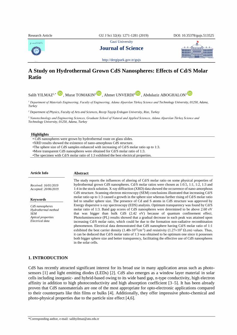
Plain view SEM images of S1, S2, S3, S4 and S5 specimens produced on glass substrates are indicated in
Figure 2(a)-(e). Figure 2(a) shows SEM data of S1 sample, suggesting that nanoscaled sphere morphology
is observed. A homogenous sphere distribution is seen besides the presence of the smallest sphere size. A
compact and dense morphology is also reached without forming any crack or void. Additionally, big sized
spheres come into existence over the smaller ones. When Cd/S molar ratio is altered from 1:0.5 to 1:1 (as
indicated in Figure 2(b)), sphere size starts increasing and undefined shape grains are also seen on the
surface of the sample. Figure 2(c) depicts the morphology related to Cd/S molar ratio of 1:2. It is appeared
that obvious and compact topography in addition to the existence of uniform sphere distribution is acquired
whereas some big spheres are still seen over the smaller ones. SEM data of S4 sample corresponding to
Cd/S molar ratio of 1:3 is demonstrated in Figure 2(d), proposing that this specimen possesses the largest
sphere size in addition to its homogenous sphere size distribution. Yet, some big grains still seem on the
surface. An enlargement in the sphere size with increasing sulfur ingredient till Cd/S molar ratio of 1:3 in
CdS could be ascribed to the highest growth regime of CdS nanosphere on glass substrates [23]. It was also
reported that a rise in the sulfur atoms in CdS matrix led to a grain growth till a critical Cd/S molar ratio
[14]. Figure 2(e) represents SEM result of S5 specimen (Cd/S molar ratio of 1:4). It is remarkable that
sphere sizes substantially reduce even though their uniform distribution is preserved. More compact
topography is also obtained. In comparison with the previous samples, further increase of sulfur atoms in
2 (degree)
10 20 30 40 50 60 70
Inte
nsi
ty (
Counts
)
0
300
600
Page 4
1274 Salih YILMAZ, Murat TOMAKIN, Ahmet UNVERDI, Abdulaziz ABOGHALON/ GU J Sci, 32(4): 1271-1281 (2019)
CdS host matrix (S5) gives rise to a reduction in the sphere size which might be referred to the growth
limitation of CdS nanospheres owing to the saturation of sulfur atoms in CdS structure [24, 14]. A declining
behavior of sphere size with dropping Cd/S molar ratio was also found by Zhao et al. for CdS thin films
grown by CBD method [25] and Lopes et al. for CdS nanospheres synthesized by sonochemical technique
[26]. Thickness evaluation is made through the cross-sectional measurement and the conclusion of S3 is
provided in Figure 2(f), implying that average thickness of the sample is about 108 nm. Figure 2(g) depicts
FESEM top-view photograph of S4 specimen, proving an obvious creation of CdS nanospheres on the glass
slides. It could be also noted from Figure 2(g) that CdS nanospheres are formed by assembling of small
nanocrystallites.
Figure 2. SEM plain view photographs of (a) S1, (b) S2, (c) S3, (d) S4 and (e) S5 specimens with a
magnification 50000x. (f) shows the cross-sectional image of S3. (g) indicates FE-SEM top-view image of
S4
(a) (b)
(c) (d)
(e) (f)
(g)
Page 5
1275 Salih YILMAZ, Murat TOMAKIN, Ahmet UNVERDI, Abdulaziz ABOGHALON/ GU J Sci, 32(4): 1271-1281 (2019)
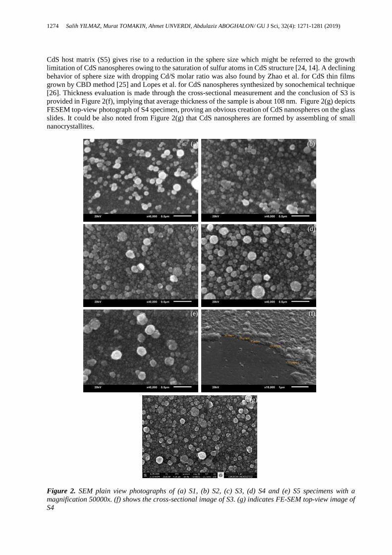
EDS survey spectra and true atomic concentrations (presented in the insets) of S1, S2, S3, S4 and S5
specimens produced on the glass slides are illustrated in Figure 3. The existence of Cd and S atoms in CdS
structure is proved by these spectra. S1 sample has Cd and S atoms with an atomic ratio of 1.07. This ratio
progressively diminishes with rising of Cd/S molar ratio up to 1:4. The lowest Cd/S atomic ratio of 0.91 is
acquired for Cd/S molar ratio of 1:4. It is attained that CdS nanospheres having Cd/S molar ratio of 1:0.5
exhibit excess of cadmium and lack of sulfur atoms. Once Cd/S molar ratio is dropped from 2 to 1, the most
stoichiometric sample is reached. Upon further reducing of Cd/S molar ratio, sulfur rich and cadmium
deficient specimens are obtained, implying that a divergence from the stoichiometry is found. It can be also
declared that it seems an analogous behavior in the alteration between atomic and molar ratios of Cd/S as
anticipated.
Figure 3. EDS data of (a) S1, (b) S2, (c) S3, (d) S4 and (e) S5 specimens. Insets of the figures indicate the
true atomic concentrations of Cd and S in the CdS nanospheres
Transparency of CdS specimens is examined by transmission analysis and the conclusions of S1, S2, S3,
S4 and S5 specimens are shown in Figure 4. S1 sample possesses a transmittance (T) value of almost 51 %
in the wavelength interval of 550-800 nm and then T takes the maximum score of 58 % at 1000 nm. When
Cd/S molar ratio is modified to 1:1 (S2 specimen), transmission substantially decreases to about 42 % and
the highest T of 48 % at 1000 nm is acquired even though the curve shape is akin to that of S1 specimen.
The deterioration in the transmittance could be attributed to the small alteration in the thickness values of
the CdS nanospheres. Zhao et al. reported a similar result in the transmission of the specimens with
(a) (b)
(c) (d)
(e)
(a)
Page 6
1276 Salih YILMAZ, Murat TOMAKIN, Ahmet UNVERDI, Abdulaziz ABOGHALON/ GU J Sci, 32(4): 1271-1281 (2019)
increasing of S/Cd molar ratio [25]. But, once Cd/S molar ratio is changed to 1:2 (S3 specimen),
transparency improves to 48 % that is still lower than that of S1. On the other hand, S4 specimen associated
with Cd/S molar ratio of 1:3 exhibits the peak T score of 55 % in the wavelength range of 550 nm - 850
nm. The enhancement in the transparency may be due to the growth in the sphere size as illustrated in
Figure 2(d). Pandya and co-workers obtained an analogous data, saying that more transparent CdS thin
films synthesized by CBD were attained with the rise of sulfur atoms in CdS specimens [19]. As the Cd/S
molar ratio is varied from 1:3 to 1:4, the transmittance plot exhibits moderately different behavior,
especially at lower wavelength region. Furthermore, transparency of CdS nanosphere is got worse for S5
sample with respect to that of S4 one. This slight degradation in the transmission is ascribed to smaller
sphere size as displayed in Figure 2(e). Eventually, it can be stated that the most transparent CdS nanosphere
is reached for S4 sample that is able to be employed in the CdTe or CIGS-based solar cells as a window
layer.
Figure 4. Transmittance plots of S1, S2, S3, S4 and S5 specimens
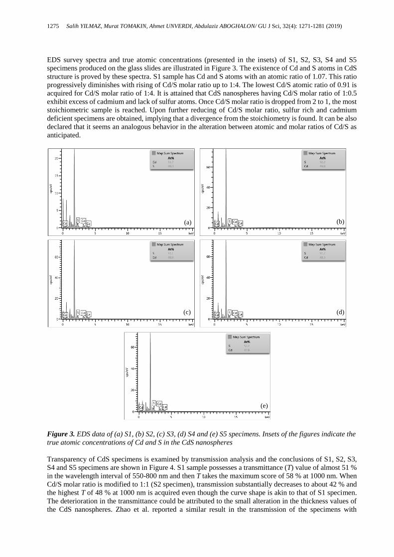
Upon reducing Cd/S molar ratio, absorption edge moves to the longer wavelength region as can be shown
in Figure 4. Band gaps of S1, S2, S3, S4 and S5 specimens are determined via Tauc’s approximation [27]
and the conclusions are given in Figure 5. It is obtained that all the samples exhibit forbidden band gaps
above 2.60 eV that is wider than that of bulk CdS (2.42 eV). The reason for boosting of the band gap of
CdS specimens is most probably due to the quantum size effect taking place at diminishing of the crystalline
size below a critical value [21]. But, XRD outcomes indicate that CdS specimens grow in the nano-
amorphous structure owing to formation in thin thickness (about 100 nm) and thus, it is difficult to calculate
the crystalline size of the specimens. On the other hand, as shown in Figure 2(g), CdS nanospheres are
formed by agglomeration of nano-sized crystallites, implying that the crystallites possess a very small grain
size. Forbidden band gap of S1 specimen is determined as 2.66 eV and when Cd/S molar ratio is modified
to 1:1 (S2 specimen), it reduces to 2.61 eV. Zhao et al. grew CdS-based thin films and found that increasing
S/Cd molar ratio led to a reduction in the band gap of the samples, which is consistent with our outputs
[25]. However, further decrease of Cd/S molar ratio till 1:2 and 1:3 brings about a little increase in the band
gap value of the specimens that is nearly 2.62 eV. On the other hand, a clear rise is attained for S5 specimen
with a band gap of 2.66 eV that is the same as that of S1. This significant variation in the band gap might
be attributed to the presence of quantum confinement effect.
Wavelength (nm)
400 500 600 700 800 900 1000
Tra
nsm
itta
nce
(%
)
0
10
20
30
40
50
60
70
S1
S2
S3
S4
S5
Page 7
1277 Salih YILMAZ, Murat TOMAKIN, Ahmet UNVERDI, Abdulaziz ABOGHALON/ GU J Sci, 32(4): 1271-1281 (2019)
Figure 5. Tauc’s curves of S1, S2, S3, S4 and S5 specimens
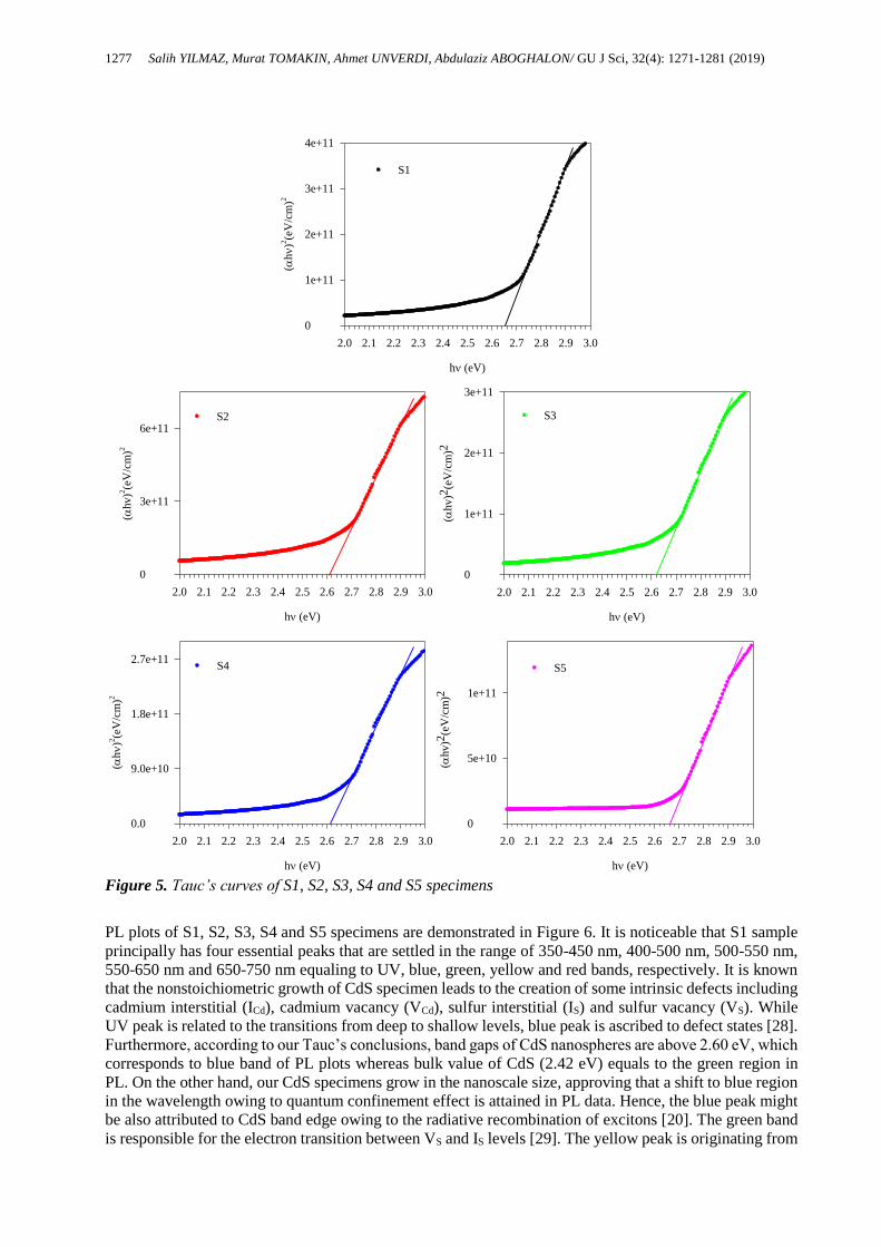
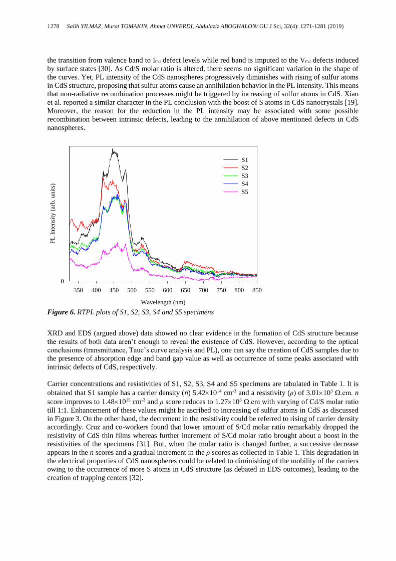
PL plots of S1, S2, S3, S4 and S5 specimens are demonstrated in Figure 6. It is noticeable that S1 sample
principally has four essential peaks that are settled in the range of 350-450 nm, 400-500 nm, 500-550 nm,
550-650 nm and 650-750 nm equaling to UV, blue, green, yellow and red bands, respectively. It is known
that the nonstoichiometric growth of CdS specimen leads to the creation of some intrinsic defects including
cadmium interstitial (ICd), cadmium vacancy (VCd), sulfur interstitial (IS) and sulfur vacancy (VS). While
UV peak is related to the transitions from deep to shallow levels, blue peak is ascribed to defect states [28].
Furthermore, according to our Tauc’s conclusions, band gaps of CdS nanospheres are above 2.60 eV, which
corresponds to blue band of PL plots whereas bulk value of CdS (2.42 eV) equals to the green region in
PL. On the other hand, our CdS specimens grow in the nanoscale size, approving that a shift to blue region
in the wavelength owing to quantum confinement effect is attained in PL data. Hence, the blue peak might
be also attributed to CdS band edge owing to the radiative recombination of excitons [20]. The green band
is responsible for the electron transition between VS and IS levels [29]. The yellow peak is originating from
h (eV)
2.0 2.1 2.2 2.3 2.4 2.5 2.6 2.7 2.8 2.9 3.0
(h
)2(e
V/c
m)2
0
1e+11
2e+11
3e+11
4e+11
S1
h (eV)
2.0 2.1 2.2 2.3 2.4 2.5 2.6 2.7 2.8 2.9 3.0
(hv)2
(eV
/cm
)2
0
3e+11
6e+11S2
h (eV)
2.0 2.1 2.2 2.3 2.4 2.5 2.6 2.7 2.8 2.9 3.0
(hv)2
(eV
/cm
)2
0
1e+11
2e+11
3e+11
S3
h (eV)
2.0 2.1 2.2 2.3 2.4 2.5 2.6 2.7 2.8 2.9 3.0
(h
)2(e
V/c
m)2
0.0
9.0e+10
1.8e+11
2.7e+11S4
h (eV)
2.0 2.1 2.2 2.3 2.4 2.5 2.6 2.7 2.8 2.9 3.0
0
5e+10
1e+11
S5
(hv)2
(eV
/cm
)2
Page 8
1278 Salih YILMAZ, Murat TOMAKIN, Ahmet UNVERDI, Abdulaziz ABOGHALON/ GU J Sci, 32(4): 1271-1281 (2019)
the transition from valence band to ICd defect levels while red band is imputed to the VCd defects induced
by surface states [30]. As Cd/S molar ratio is altered, there seems no significant variation in the shape of
the curves. Yet, PL intensity of the CdS nanospheres progressively diminishes with rising of sulfur atoms
in CdS structure, proposing that sulfur atoms cause an annihilation behavior in the PL intensity. This means
that non-radiative recombination processes might be triggered by increasing of sulfur atoms in CdS. Xiao
et al. reported a similar character in the PL conclusion with the boost of S atoms in CdS nanocrystals [19].
Moreover, the reason for the reduction in the PL intensity may be associated with some possible
recombination between intrinsic defects, leading to the annihilation of above mentioned defects in CdS
nanospheres.
Figure 6. RTPL plots of S1, S2, S3, S4 and S5 specimens
XRD and EDS (argued above) data showed no clear evidence in the formation of CdS structure because
the results of both data aren’t enough to reveal the existence of CdS. However, according to the optical
conclusions (transmittance, Tauc’s curve analysis and PL), one can say the creation of CdS samples due to
the presence of absorption edge and band gap value as well as occurrence of some peaks associated with
intrinsic defects of CdS, respectively.
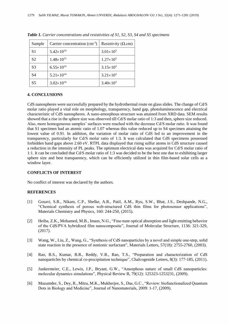
Carrier concentrations and resistivities of S1, S2, S3, S4 and S5 specimens are tabulated in Table 1. It is
obtained that S1 sample has a carrier density (n) 5.421014 cm-3 and a resistivity (ρ) of 3.01103 Ω.cm. n
score improves to 1.481015 cm-3 and ρ score reduces to 1.27103 Ω.cm with varying of Cd/S molar ratio
till 1:1. Enhancement of these values might be ascribed to increasing of sulfur atoms in CdS as discussed
in Figure 3. On the other hand, the decrement in the resistivity could be referred to rising of carrier density
accordingly. Cruz and co-workers found that lower amount of S/Cd molar ratio remarkably dropped the
resistivity of CdS thin films whereas further increment of S/Cd molar ratio brought about a boost in the
resistivities of the specimens [31]. But, when the molar ratio is changed further, a successive decrease
appears in the n scores and a gradual increment in the ρ scores as collected in Table 1. This degradation in
the electrical properties of CdS nanospheres could be related to diminishing of the mobility of the carriers
owing to the occurrence of more S atoms in CdS structure (as debated in EDS outcomes), leading to the
creation of trapping centers [32].
Wavelength (nm)
350 400 450 500 550 600 650 700 750 800 850
PL
In
ten
sity
(ar
b.
unit
s)
0
S1
S2
S3
S4
S5
Page 9
1279 Salih YILMAZ, Murat TOMAKIN, Ahmet UNVERDI, Abdulaziz ABOGHALON/ GU J Sci, 32(4): 1271-1281 (2019)
Table 1. Carrier concentrations and resistivities of S1, S2, S3, S4 and S5 specimens
Sample Carrier concentration (cm-3) Resistivity (Ω.cm)
S1 5.421014 3.01103
S2 1.481015 1.27103
S3 6.551014 3.15103
S4 5.211014 3.21103
S5 3.021014 3.40103
4. CONCLUSIONS
CdS nanospheres were successfully prepared by the hydrothermal route on glass slides. The change of Cd/S
molar ratio played a vital role on morphology, transparency, band gap, photoluminescence and electrical
characteristic of CdS nanospheres. A nano-amorphous structure was attained from XRD data. SEM results
showed that a rise in the sphere size was observed till Cd/S molar ratio of 1:3 and then, sphere size reduced.
Also, more homogeneous samples’ surfaces were reached with the decrease Cd/S molar ratio. It was found
that S1 specimen had an atomic ratio of 1.07 whereas this value reduced up to S4 specimen attaining the
lowest value of 0.91. In addition, the variation of molar ratio of CdS led to an improvement in the
transparency, particularly for Cd/S molar ratio of 1:3. It was calculated that CdS specimens possessed
forbidden band gaps above 2.60 eV. RTPL data displayed that rising sulfur atoms in CdS structure caused
a reduction in the intensity of PL peaks. The optimum electrical data was acquired for Cd/S molar ratio of
1:1. It can be concluded that Cd/S molar ratio of 1:3 was decided to be the best one due to exhibiting larger
sphere size and best transparency, which can be efficiently utilized in thin film-based solar cells as a
window layer.
CONFLICTS OF INTEREST
No conflict of interest was declared by the authors.
REFERENCES
[1] Gosavi, S.R., Nikam, C.P., Shelke, A.R., Patil, A.M., Ryu, S.W., Bhat, J.S., Deshpande, N.G.,
“Chemical synthesis of porous web-structured CdS thin films for photosensor applications”,
Materials Chemistry and Physics, 160: 244-250, (2015).
[2] Heiba, Z.K., Mohamed, M.B., Imam, N.G., “Fine-tune optical absorption and light emitting behavior
of the CdS/PVA hybridized film nanocomposite”, Journal of Molecular Structure, 1136: 321-329,
(2017).
[3] Wang, W., Liu, Z., Wang, G., “Synthesis of CdS nanoparticles by a novel and simple one-step, solid
state reaction in the presence of nonionic surfactant”, Materials Letters, 57(18): 2755-2760, (2003).
[4] Rao, B.S., Kumar, B.R., Reddy, V.R., Rao, T.S., “Preparation and characterization of CdS
nanoparticles by chemical co-precipitation technique”, Chalcogenide Letters, 8(3): 177-185, (2011).
[5] Junkermeier, C.E., Lewis, J.P., Bryant, G.W., “Amorphous nature of small CdS nanoparticles:
molecular dynamics simulations”, Physical Review B, 79(12): 125323-1253231, (2009).
[6] Mazumder, S., Dey, R., Mitra, M.K., Mukherjee, S., Das, G.C., “Review: biofunctionalized Quantum
Dots in Biology and Medicine”, Journal of Nanomaterials, 2009: 1-17, (2009).
Page 10
1280 Salih YILMAZ, Murat TOMAKIN, Ahmet UNVERDI, Abdulaziz ABOGHALON/ GU J Sci, 32(4): 1271-1281 (2019)
[7] Baghchesara, M.A., Yousefi, R., Cheraghizade, M., Sheini, F.J., Saaedi, A., “Photocurrent
application of Zn-doped CdS nanostructures grown by thermal evaporation method”, Ceramics
International, 42(1): 1891-1896, (2016).
[8] Zhao, J.G., Hua, Z.H., Yao, Y., “Solvothermal synthesis and characterization of one-dimensional
CdS nanowires”, Superlattices and Microstructures, 61: 146-151, (2013).
[9] Guo, X., Chen, C., Song, W., Wang, X., Di, W., Qin, W., “CdS embedded TiO2 hybrid nanospheres
for visible light photocatalysis”, Journal of Molecular Catalysis A: Chemical, 387: 1-6, (2014).
[10] Wang, Y., Yang, X., Ma, Q., Kong, J., Jia, H., Wang, Z., Yu, M., “Preparation of flower - like CdS
with SDBS as surfactant by hydrothermal method and its optical properties”, Applied Surface
Science, 340: 18-24, (2015).
[11] Tang, K.B., Qian, Y.T., Zeng, J.H., Yang, X.G., “Solvothermal Route to Semiconductor Nanowires”,
Advanced Materials, 15: 448-450, (2003).
[12] Niasari, M.S., Estarki, M.R.L., Davar, F., “Controllable synthesis of nanocrystalline CdS with
different morphologies by hydrothermal process in the presence of thioglycolic acid”, Chemical
Engineering Journal, 145(2): 346-350, (2008).
[13] Zhai, T., Fang, X., Li, L., Bando, Y., Golberg, D., “One-dimensional CdS nanostructures: synthesis,
properties, and applications”, Nanoscale, 2: 168-187, (2010).
[14] Datta, A., Kar, S., Ghatak, J., Chaudhuri, S., “Solvothermal synthesis of CdS nanorods: Role of basic
experimental parameters”, Journal of Nanoscience and Nanotechnology, 7(2): 677-688, (2007).
[15] Vazquez, A., Serrano, T., Kharisov, B., Gomez, I., “Morphological control of cadmium sulfide
nanostructures by electrophoretic deposition”, Particuology, 24: 73-77, (2016).
[16] Pandya, S., Raval, K., “Investigation of structural, morphological and optical properties of cadmium
sulphide (CdS) thin films at different Cd/S concentration deposited by chemical technique”, Journal
of Materials Science: Materials in Electronics, 28(23): 18031-18039, (2017).
[17] Kumar, V., Rajaram, P., Goswami, Y.C., “Sol–gel synthesis of SnO2/CdS heterostructures using
various Cd:S molar ratio solutions and its application in photocatalytic degradation of organic dyes”,
Journal of Materials Science: Materials in Electronics, 28(12): 9024-9031, (2017).
[18] Yuan, X., Li, M., Ruan, H., Yang, Y., Liu, Y., Zhang, L., “CdS nanoparticles with high photocatalytic
property synthesized by a new liquid–liquid method”, Journal of Materials Science: Materials in
Electronics, 27(6): 6030-6034, (2016).
[19] Xiao, Q., Xiao, C., “Surface-defect-states photoluminescence in CdS nanocrystals prepared by one-
step aqueous synthesis method”, Applied Surface Science, 255(16): 7111-7114, (2009).
[20] Thambidurai, M., Murugan, N., Muthukumarasamy, N., Agilan, S., Vasantha, S.,
Balasundaraprabhu, R., “Influence of the Cd/S Molar Ratio on the Optical and Structural Properties
of Nanocrystalline CdS Thin Films”, Journal of Materials Science & Technology, 26(3): 193-199,
(2010).
[21] Kumar, S., Sharma, P., Sharma, V., “Structural transition in II-VI nanofilms: Effect of molar ratio
on structural, morphological, and optical properties”, Journal of Applied Physics, 111(11): 113510-
113517, (2012).
[22] Rosales, K.R., Galvan, J.G.Q., Cervantes, A.G., Gonzalez, E.C., Cruz, J.S., Hernandez, S.A.M.,
Ceron, J.S.A., Olvera, M.D.L.L., Angel, O.Z., Hernandez, L.A.H., Puente, G.C., Flores, F.D.M.,
Page 11
1281 Salih YILMAZ, Murat TOMAKIN, Ahmet UNVERDI, Abdulaziz ABOGHALON/ GU J Sci, 32(4): 1271-1281 (2019)
“Nanocrystalline-CdS thin films grown on flexible PET-substrates by chemical bath deposition”,
Materials Research Express, 4(7): 075904-075911, (2017).
[23] Cao, M., Suna, Y., Wua, J., Chena, X., Daia, N., “Effects of cadmium salts on the structure,
morphology and optical properties of acidic chemical bath deposited CdS thin films”, Journal of
Alloys and Compounds, 508(2): 297-300, (2010).
[24] Lin, G., Zheng, J., Xu, R., “Template-free synthesis of uniform CdS hollow nanospheres and their
photocatalytic activities”, The Journal of Physical Chemistry C, 112(19): 7363-7370, (2008).
[25] Zhao, X.H., Wei, A.X., Zhao, Y., Liu, J., “Structural and optical properties of CdS thin films prepared
by chemical bath deposition at different ammonia concentration and S/Cd molar ratios”, Journal of
Materials Science: Materials in Electronics, 24(2): 457-462, (2013).
[26] Lopes, P.A.L., Santos, M.B., Mascarenhasa, A.J.S., Silva, L.A., “Synthesis of CdS nano-spheres by
a simple and fast sonochemical method at room temperature”, Materials Letters, 136: 111-113,
(2014).
[27] Tauc, J., Grigorovici, R., Vancu, A., “Optical properties and electronic structure of amorphous
germanium”, Physica Status Solidi B, 15: 627-637, (1966).
[28] Kumar, R., Das, R., Gupta, M., Ganesan, V., “Compositional effect of antimony on structural,
optical, and photoluminescence properties of chemically deposited (Cd1−xSbx)S thin films”,
Superlattices and Microstructures, 59: 29-37, (2013).
[29] Kumar, P., Saxena, N., Chandra, R., Gao, K., Zhou, S., Agarwal, A., Singh, F., Gupta, V., Kanjilal,
D., “SHI induced enhancement in green emission from nanocrystalline CdS thin films for photonic
applications”, Journal of Luminescence, 147: 184-189, (2014).
[30] Ji, X., Li, H., Cheng, S., Wu, Z., Xie, Y., Dong, X., Yan, P., “Growth and photoluminescence of CdS
and CdS:Mn Nanoribbons”, Materials Letters, 65(17-18): 2776-2778, (2011).
[31] Cruz, J.S., Perez, R.C., Delgado, G.T., Angel, O.Z., “CdS thin films doped with metal-organic salts
using chemical bath deposition”, Thin Solid Films, 518(7): 1791-1795, (2010).
[32] Yilmaz, S., Polat, I., Atasoy, Y., Bacaksiz, E., “Structural, morphological, optical and electrical
evolution of spray deposited ZnO rods co-doped with indium and sulphur atoms”, Journal of
Materials Science Materials in Electronics, 25(4): 1810-1816, (2014).