M. Lalitha Sowmya, B.Divya, S.Jag adeesh / International Journal of Engineering Re search and Applications (IJERA) ISSN: 2248-9622 www.ijera.comVol. 2, Issue 5, September- October 2012, pp.1718-1724 1718 | P a g e Design of Custom Instructions in Cryptograph ic Processor M. Lalitha Sowmya 1 , B.Divya 2 , S.Jagadeesh 3 (Assistant Professor, Department o f ECE, SSJ Engineering College, JNTU , Ga ndipet.) (MTech Student, Department of ECE, SSJ Engineering College, JN TU, G andipet.) (Associate Professor and H.O.D, Department of ECE, SSJ Engineering College, JNTU, Gandipet.) Abstract In this paper, we are implementing 32 bit pipelined processor on FPGA and designed using verilog. In this Processor , we had performed logical operations and arithmetic operations like rotate word, modular addition modular multiplication, matrix multiplication, fixed coefficient multiplier ,mix column transform using binary extension field operations (2^m) for arbitrary irreduci ble Polynomial. Using ou r proposed field a rithmetic units we can implement Symmetric Key Cryptography algorithms . Experimental Results Sh ows that developed processor working with high Speed , low area and low path delay . Keywords: Cryptographic Processor, Pipeline, Finite field arithmetic (FFA), Symmetric Key Cryptography algorithms. 1. Intro duction The explosive growth in data communications and Internet services have made cryptography an important research topic. Cryptography is used for confidentiality, authentication, data integrity, and non-repudiation, which can be divided into two families: Asymmetric key cryptography: In public key cryptography, the data that is encrypted with the public key can only be decrypted with the corresponding private key. Symmetric key cryptography: The process ofencryption and decryption of information by using a single key is known as Symmetric Key Cryptography. These are based on a mathematical function to encrypt a plain-text message and to produce cipher message. [8] In this Paper we are designing Symmetric key mathematical operations in a 32 bit pipelined processor. Implementing Symmetric Key operations in software seems to not only too slow for fast application such as Routers but also vulnerable to attacks. In contrast, in Hardware implementation, the higher data rate (G bits/second) is made possible by parallel and/or pipelining processing. Moreover, the implementations are physically Secure since tempering by an outside attacker is Difficult. With these supporting reasons we are looking at the hardware implementation. Implementing various symmetric-Key operations in a general-purpose Processor (GPP) is flexible but requires a lower throughput rate, more clock cycles for each instruction, more no. of addressing modes and larger power Consumption. So we developed processor that the instruction set can be hardwired to speed instruction execution. No microcode is needed for single cycle execution. All instructions are one word (fixed bit) in length. This simplifies the instruction fetch mechanism since the location of instruction boundaries is not a function of the instruction type. The processor has small number of addressing modes. Only load and store instructions access memory. There are no computational instructions that access memory; load/store instructions operate between memory and a register. Control hardware is simplified and the machine cycle time is minimized. The remainder of this paper is organized as follows. Section 2: Algorithms of Symmetric Key operations. Section 3: Implementation ofOperations. Section 4Proposed Architecture. Section 5: Modules design of ALU, Control unit, Multiplexers and general purpose registers. Section 6. Results. Section7: Conclusion Section 8: References. 2. Cryptographic algorithms for symmetric block ciphers. Advanced Encryption Standard (AES), RC6, RC5, Data Encryption Standard (DES), Blowfish, International Data Encryption Algorithm (IDEA). Blowfishis a symmetric block cipher that encrypts data in 8-byte (64-bit) blocks [3]. The algorithm has two parts, key expansion and data encryption. Key expansion consists ofgenerating the initia l contents of one array Namely, eighteen 32-bit sub-keys, and four arrays (the S-boxes), each of size 256 by 32 bits, from a key of at most 448 b its (56 bytes). The data encryption uses a 16-round Feistel Network .The F Function, regarded as the Primary source of algorithm security [3], combines two simple functions: Addition modulo two (XOR) and Addition modulo 2^32.
Transcript
7/31/2019 Js 2517181724
http://slidepdf.com/reader/full/js-2517181724 1/7
M. Lalitha Sowmya, B.Divya, S.Jagadeesh / International Journal of Engineering Research
and Applications (IJERA) ISSN: 2248-9622 www.ijera.com Vol. 2, Issue 5, September- October 2012, pp.1718-1724
1718 | P a g e
Design of Custom Instructions in Cryptographic Processor
M. Lalitha Sowmya1, B.Divya2, S.Jagadeesh3
(Assistant Professor, Department of ECE, SSJ Engineering College, JNTU , Gandipet.)(MTech Student, Department of ECE, SSJ Engineering College, JNTU, Gandipet.)
(Associate Professor and H.O.D, Department of ECE, SSJ Engineering College, JNTU, Gandipet.)
AbstractIn this paper, we are implementing 32
bit pipelined processor on FPGA and designedusing verilog. In this Processor , we hadperformed logical operations and arithmeticoperations like rotate word, modular additionmodular multiplication, matrix multiplication,fixed coefficient multiplier ,mix columntransform using binary extension field operations(2^m) for arbitrary irreducible Polynomial.
Using our proposed field arithmetic units wecan implement Symmetric Key Cryptographyalgorithms . Experimental Results Shows thatdeveloped processor working with high Speed ,low area and low path delay .
Keywords: Cryptographic Processor, Pipeline,Finite field arithmetic (FFA), Symmetric KeyCryptography algorithms.
1. IntroductionThe explosive growth in data
communications and Internet services have madecryptography an important research topic.Cryptography is used for confidentiality,authentication, data integrity, and non-repudiation,
which can be divided into two families:Asymmetric key cryptography: In public keycryptography, the data that is encrypted with the
public key can only be decrypted with thecorresponding private key.Symmetric key cryptography: The process of
encryption and decryption of information by using asingle key is known as Symmetric KeyCryptography. These are based on a mathematical
function to encrypt a plain-text message and toproduce cipher message. [8]In this Paper we are designing Symmetric
key mathematical operations in a 32 bit pipelinedprocessor.
Implementing Symmetric Key operations
in software seems to not only too slow for fastapplication such as Routers but also vulnerable toattacks. In contrast, in Hardware implementation,the higher data rate (G bits/second) is made possible
by parallel and/or pipelining processing. Moreover,the implementations are physically
Secure since tempering by an outside attacker is
Difficult. With these supporting reasons we arelooking at the hardware implementation.
Implementing various symmetric-Key operations ina general-purpose Processor (GPP) is flexible but
requires a lower throughput rate, more clock cyclesfor each instruction, more no. of addressing modesand larger power Consumption.
So we developed processor that the
instruction set can be hardwired to speed instructionexecution. No microcode is needed for single cycleexecution. All instructions are one word (fixed bit)
in length. This simplifies the instruction fetchmechanism since the location of instruction
boundaries is not a function of the instruction type.The processor has small number of addressingmodes. Only load and store instructions accessmemory. There are no computational instructions
that access memory; load/store instructions operatebetween memory and a register. Control hardware issimplified and the machine cycle time is minimized.
The remainder of this paper is organized asfollows. Section 2: Algorithms of Symmetric Keyoperations. Section 3: Implementation of
Operations. Section 4 Proposed Architecture.Section 5: Modules design of ALU, Control unit,Multiplexers and general purpose registers. Section6. Results. Section7: Conclusion Section 8:References.
2. Cryptographic algorithms for symmetricblock ciphers.
Advanced Encryption Standard (AES),RC6, RC5, Data Encryption Standard (DES),Blowfish, International Data Encryption Algorithm
(IDEA).
Blowfish is a symmetric block cipher that
encrypts data in 8-byte (64-bit) blocks [3]. Thealgorithm has two parts, key expansion and dataencryption. Key expansion consists of generating the initial contents of one array
Namely, eighteen 32-bit sub-keys, and four arrays(the S-boxes), each of size 256 by 32 bits, from akey of at most 448 bits (56 bytes). The data
encryption uses a 16-round Feistel Network .The FFunction, regarded as the
Primary source of algorithm security [3],
combines two simple functions: Addition modulotwo (XOR) and Addition modulo 2^32.
7/31/2019 Js 2517181724
http://slidepdf.com/reader/full/js-2517181724 2/7
M. Lalitha Sowmya, B.Divya, S.Jagadeesh / International Journal of Engineering Research
and Applications (IJERA) ISSN: 2248-9622 www.ijera.com Vol. 2, Issue 5, September- October 2012, pp.1718-1724
1719 | P a g e
AES [2] is a block cipher developed in effort toaddress threatened key size of Data EncryptionStandard (DES).It allows the data length of 128, 192and 256 bits, and supporting three different key
lengths, 128, 192, and 256 bits. AES can be dividedinto four basic operation blocks where data are
treated at either byte or bit level. The array of bytesorganized as a 4×4 matrix is also called "state" andthose four basic steps;, Bytes Sub Shift Row or
Rotate Word, Matrix Multiplication, MixColumn, and AddRoundKey are also known aslayers. These four layer steps describe one round of
the AES. The number of rounds is depended on thekey length, i.e., 10, 12 and 14 rounds for the keylength of 128, 192 and 256 bits respectively.
RC5 is exactly designated as RC5-w/r/b,where the variable parameters w, r, and brespectively denote the Word size (in bits), the
number of rounds, and the length of secret key (inbytes). The allowable value of w is 16, 32 and 64;
the allowable values of r and b range from 0 to 255.The parameter of RC5-32/12/16 is commonlychosen there are three routines in RC5: keyexpansion, encryption, and decryption. These
routines consist of three primitive operations (andtheir inverse): words addition , bitwise XOR,
and data-dependent left rotation of x by ydenoted by x <<< y. Note that only the log2(w)low order bits of y affect this rotation. In thekey-expansion routine, the user provided secret keyis expanded to fill a key table whose size depends
on the number of rounds. The key table is then usedin both encryption and decryption.
RC6 [7] is a symmetric-key algorithmwhich encrypts 128-bit plaintext blocks to 128-bit
cipher text blocks. The encryption process involves
four operations: Integer addition modulo 2W
,
Bitwise exclusive or of two w-bit words,. Rotationto the left, and
f( X ) = ( X (2 X + 1)) mod 2W
.
IDEA [8] algorithm of the encryption
process, we provide the original (128bits) cipher keyto the mentioned unit. When necessary, the KeyGenerator Unit produces different sub-keys by
performing circular left shift operation (by 25bits) on the current key and provides the sub-keys toother units. The unit named as “Multiplication
modulo 216 + 1”, is used to perform all the
multiplication modulo 2^16+1 operation, whenrequired. The same is for unit“Addition modulo 2^16” and unit “Bitwise
XOR”. or the parallel implementation of IDEA
algorithm, the entire encryption process can beperformed in several steps and performing
operations in parallel wherever possible. Parallelismin operations can be achieved both in software andusing hardware.
3. Implementation of Algorithm operations.
3.1 Modular Addition Two.The addition of two elements in a finite
field is achieved by “adding” the coefficients for the
corresponding powers in the polynomials for thetwo elements. The addition isPerformed with the XOR operation (denoted by )
i.e., modulo 2 -so that 1 1 = 0, 1 0 = 1, and 00 = 0.
Require: Binary Polynomials a (z), b (z) withmaximum degree m-1.Ensure: c (z) =a (z) + b (z).
1: for i from 0 to M-1 do
2: C[i] A[i] B[i].3: end for
4: Return(c).
3.2 .Modular Multiplication 2^8In the polynomial representation,
multiplication in GF 2^8 (denoted by •) correspondswith the multiplication of polynomials modulo anirreducible polynomial of degree 8. A polynomialis irreducible if its only divisors are one and itself.For the AES algorithm, this irreducible polynomial
ism(x) = x
8.
. For Example,{57}.{83}={C1},because
(x6 + x + x2 +x +1) (x 7 + x + 1) =
x13
+ x11
+ x9
+ x8
+ x7
+ x7
+ x5+ x
3+x
2+ x +
x 6 + x 4 + x 2 + x + 1 =
x13
+ x11
+ x9+ x
8+ x
6+ x
5+ x
4+ x
3+ 1.
Andx 13+ x 11+ x 9 + x8 + x 6 + x 5 + x 4 + x 3 + 1 modulo
x8..
In Prime Field operations modulo means divide itrequires more time .so in binary field operation it
operates on the state column-by-column as a four-term polynomial .The columns are considered as
polynomials over GF(2^8) and multiplied modulox^4 + 1 with a fixed polynomial a( x), given by a( x)
= {03} x3
+ {01} x2
+ {01} x + {02} .
7/31/2019 Js 2517181724
http://slidepdf.com/reader/full/js-2517181724 3/7
M. Lalitha Sowmya, B.Divya, S.Jagadeesh / International Journal of Engineering Research
and Applications (IJERA) ISSN: 2248-9622 www.ijera.com Vol. 2, Issue 5, September- October 2012, pp.1718-1724
1720 | P a g e
Fig 1: Mix Column Transform.
To derive a suitable Mix Column transform
architecture, the trans formation matrix given inFig can be rewritten as s’(x) =s(x) .a(x)mod(x
4 + 1),,where • denotes finite field polynomial
multiplication i.e.,
As a result of this multiplication, the four bytes in acolumn are replaced by the following.
S10,c = ( {02} .So,c) ({03} .S1,c) S2,c S3,c
S11,c = So,c ({02} .S1,c) ({03} .S2,c ) S3,c
S12,c = .So,c S1,c ({02} . S2,c ) ({03} .S3,c)
S13,c = ({03} .So,c) .S1,c S2,c ({02}.S3,c)
Fig .2 Mix Columns Transform Architecture
There are many ways to implement a finite
field multiplier. An originally proposed one in theAES takes the form of XTime ( ) which isessentially multiplied by x or left-shift with {1B}feedback. That could imply either a bit-serial or abit-parallel architecture. Rudra [3] proposed the
implementation of Rijndael system with compositefield arithmetic. We are considering a fastmultiplier, simple, small area, and support pipeline
architecture (if needed). Notice of the fix-valuemultiplications (by {02} or by {03}) leads us to afixed-coefficient multiplication in GF (2^8) that
fulfils our requirements. We are investigating thismultiplier...
3.5. Fixed Coefficients Multiplier.Let Si, c = B(x) be an element to be multiplied. B(x)
can also be written in the polynomial form as;
B (x ) = b0 + b1x + b 2 x 2 + b 3 x3 + b4 x4 b 5 x
5+ b 6 x
6+ b 7 x
7(Eq 3.5.1)
Where b € (0,1).
Multiplications used in the Mix Column
transformation are {03}.B( x) = ( x+1 )B( x ) and{02}.B( x ) = x.B ( x ).The resulted multiplications are:
{03}.B (x ) = (b0 b7 ) + (b0 b1)x + (b1 b2) x2
+ (b2 b3 )x3+ (b3 b4) x
4+ (b4 b5 ) x
5+
(b5 b6) x
6
+ (b6 b7 ) x
7
. (Eq: 3.5.2){02}.B(x) = b7 + (b0) x + b 1 x2
+ b 2 x3
+ b3 x4
+ b 4 x5
+ b 5x6+b6 x
7(Eq 3.5.3)
Implementations of above equations aresimple since Additions are simply XORs. As anexample the circuit to Compute x.Bi is shown in
Fig (3) below. The implementation of (x + 1) Bishown in Fig (4). Can be done similarly. Accordingto terms given in (2), and an architecture shown inFig.(4) , the maximum delay time is expected to be
that of the a delay unit of a 2-input XOR gate.
Fig 3: A×2 Fixed Coefficient Multiplier.
Fig 4: A×3 Fixed Coefficient Multiplier.
7/31/2019 Js 2517181724
http://slidepdf.com/reader/full/js-2517181724 4/7
M. Lalitha Sowmya, B.Divya, S.Jagadeesh / International Journal of Engineering Research
and Applications (IJERA) ISSN: 2248-9622 www.ijera.com Vol. 2, Issue 5, September- October 2012, pp.1718-1724
1721 | P a g e
3.6 Multiplier X (2X + 1) Modulo 2^8.
Let,
X = b0 + b1x + b 2 x2+ b 3 x
3+ b4 x
4
b 5 x5+ b 6 x
6+ b 7 x
7 .(Eq 3.6.1)
Now,
{02}.B(x) + 1 = (b7+ 1) + (b0) x + b 1 x2
+ b 2 x3
+b3 x
4+ b 4 x
5+ b 5x
6+ b6 x
7(Eq 3.6.2)
x. ({02}.x + 1} mod 28 = x. ({02}. {x} +1) x 8
(Eq 3.6.3)
Eq (3.6.3), operation requires less time to implement
Rc6 Algorithm.
3.7 Shift Row Transform.
In the Shift Rows() transformation, the
bytes in the last three rows of the State arecyclically shifted overDifferent numbers of bytes.
Fig 5. Shift Rows Architecture.
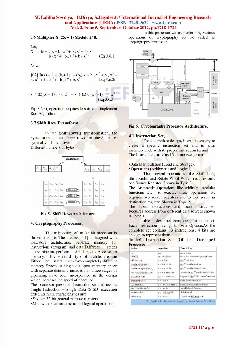
4. Cryptography Processor.
The architecture of an 32 bit processor isshown in Fig 6. The processor [1] is designed with
load/store architecture. Separate memory forinstructions (program) and data Different stagesof the pipeline perform simultaneous Accesses tomemory. This Harvard style of architecture canEither be used with two completely differentmemory Spaces, a single dual-port memory spacewith separate data and instruction.. Three stages of
pipelining have been incorporated in the designwhich increases the speed of operation.The processor presented instruction set and uses a
Single Instruction – Single Data (SISD) executionorder. Its main characteristics are:• Sixteen 32-bit general purpose registers.
•ALU with basic arithmetic and logical operations.
In this processor we are performing variousoperations of cryptography so we called ascryptography processor.
Fig 6. Cryptography Processor Architecture.
4.1 Instruction Set.For a complete design, it was necessary to
create a specific instruction set and its ownassembly code with its proper instruction format.The Instructions are classified into two groups.
•Data Manipulation (Load and Storage).• Operations (Arithmetic and Logical).
The Logical operations like Shift Left,Shift Right, and Rotate Word Which requires only
one Source Register. Shown in Type 3.The Arithmetic Operations like addition ,modularfunctions ,etc to execute these operations werequires two source registers and to tore result in
destination register. Shown in Type 2.The Load instructions and store instructionsRequires address from different data sources shown
in Type 1.Table 1 describes complete Instruction set.
Each Instruction having its own Opcode.As the
complete set contains 13 instructions; 4 bits areenough to represent them.
Table:1 Instruction Set Of The Developed
Processor.
7/31/2019 Js 2517181724
http://slidepdf.com/reader/full/js-2517181724 5/7
M. Lalitha Sowmya, B.Divya, S.Jagadeesh / International Journal of Engineering Research
and Applications (IJERA) ISSN: 2248-9622 www.ijera.com Vol. 2, Issue 5, September- October 2012, pp.1718-1724
1722 | P a g e
Type1.
31 29 2524 2019 1615 0
Type2.
31 29 2524 2019 1615 0
Type3.
31 29 2524 2019 1615 0
5. Modules Design of Architecture.
5.1 Control Unit.The control unit design is based on using
FSM (Finite State Machine) and we designed it in away that allows each state to run at one clock cycle,the first state is the reset which is initializes the CPU
internal registers and variables. The machine goes tothe reset state by enabling the reset signal for acertain number of clocks. Following the reset state
Would be the instruction fetching and decodingstates which will enable the appropriate signals forreading instruction data from the ROM thendecoding the parts of the instruction. The decodingstate will also select the next state depending on the
instruction, since every instruction has its own set of states, the control unit will jump to the correct statebased on the instruction given. After all states of arunning instruction are finished, the last one willreturn to the fetch state which will allow us to
process the next instruction in the program. Fig7:shows the state diagram for the control unit.
Fig 7. State Diagram of Control Unit.
Fig 8: Top Block of Control and Decode.
5.2 General Purpose Registers.General Purpose Registers (GPRs) store
and save operands And results during program
execution. ALU and memories must be able towrite/read those registers, so a set of Sixteen 32-bit
registers were used, along with multiplexers andcontrol& decoder which register is read or written.These two registers are the Operands to ALU which
performs the operation.
Fig 9: Simulated Timing diagram of GeneralPurpose Registers.
5.3 Instruction Register.Instruction registers store the instruction
which read from the program memory, and keep itas an output for the decoder, which separates theoperation code, Source Registers, Operand address
and operands and these values will set to Generalpurpose registers, Multiplexers and ALU to execute
the command. This is achieved simply using buffersto translate data to/from the processor.
Fig 10: Simulated Timing diagram of InstructionRegister
5.4 Arithmetic logical unit (ALU).The Arithmetic-Logic Unit has 12
operations; each one of them was created and
converted into a symbol, then, a multiplexor wasplaced in order to obtain a 4 bit selector
The ALU design comprises of 2 units. One unit ismeant for logic operation and the other unit ismeant f or Arithmetic operations shown in Table .1.
7/31/2019 Js 2517181724
http://slidepdf.com/reader/full/js-2517181724 6/7
M. Lalitha Sowmya, B.Divya, S.Jagadeesh / International Journal of Engineering Research
and Applications (IJERA) ISSN: 2248-9622 www.ijera.com Vol. 2, Issue 5, September- October 2012, pp.1718-1724
1723 | P a g e
Fig 11: Top Block of ALU
Fig 12: Simulated Timing diagram of ALU.
Fig 13: Top Block of 32 Bit Processor.
6. Results: The ISE of the 32 bit processor was
described using the Verilog .The tool chain
including the Active HDL simulator and synthesizedwith the Xilinx 9.2i tool;
After synthesized the Hardware resource
consumption for the complete processorimplemented in a Xilinx Virtex4 XC4VlX15-
12Sf363 FPGA is shown in Table 2, The number of slice flip flops utilization is minimal due to thecombinational nature of the processor being capable
of executing an instruction in few clock cycles.
Table 2: Hardware Resource Consumed
For complete processor the totalequivalent gate count for the complete processor is14,518 gates , Maximum combinational path delayis 6.509ns Maximum Frequency : 92.659MHz ,
the area utilized only 13%.
7. Conclusion.Thus the 32 bit cryptographic Processor
perform mathematical computations used in
Symmetric Key Algorithms has been designed usingverilog the simulations are done with Active HDLsimulator. The design is verified through exhaustive
simulations. Thus processor architecture followsthat one instruction executes in one clock cycle. Bythis we increase overall performance of the speedwith low area and low propagation delay. In order toobtain a more sophisticated architecture is necessaryto add some advanced techniques pipelining this
processor can also perform floating point operations.And differential equations. Apart from this it can beused in portable gaming kits, Smart cards, ATMs.
References.[1] Antonio H. Zavala “ RISC Based
Architecture for Computer Hardware
Introduction Edición,, 2011 IEEE.[2] NIST, " Advanced Encryption Standard
(AES), (FIPPUB 197)", November 26,2001, http://csrc.nist.gov/publications/.
[3] A. Rudra et. al., "Efficient Implementation
of Rijndael Encryption with Composite
Field Arithmetic", Proc.CHES2001, LNCSVol. 2162, pp.175-188, 2001.
[4] Rohit Sharma, Vivek Kumar Sehgal, NitinNitin1, Pranav Bhasker, Ishita Verma,2009, “ Design And Implementation Of 64-
Bit RISC Processor Using Computer
Modeling And Simulation, pp. 568 – 573.
[5] R. Uma / International Journal of Engineering Research and Applications(IJERA) ISSN: 2248-9622 www.ijera.com


![[2015/2016] Require JS and Handlebars JS](https://static.documents.pub/doc/80x56/58efafb91a28abf42a8b462d/20152016-require-js-and-handlebars-js.jpg)