June 2005 Computer Architecture, Background and Motivation Slide 1 1.1 Signals, Logic Operators, and Gates Figure 1.1 Some basic elements of digital logic circuits, with operator signs used in this book highlighted. x y AND Nam e XOR OR NOT G raphical sym bol x y O perator sign and alternate(s) x y x y xy x y x x orx _ x y or xy Arithm etic expression x y 2 xy x y xy 1 x O utput is 1 iff: Inputis 0 B oth inputs are 1s A tleastone inputis 1 Inputs are notequal
Transcript
June 2005 Computer Architecture, Background and Motivation Slide 1
1.1 Signals, Logic Operators, and Gates
Figure 1.1 Some basic elements of digital logic circuits, with operator signs used in this book highlighted.
x y
AND Name XOR OR NOT
Graphical symbol
x y
Operator sign and alternate(s)
x y x y xy
x y
x x or x
_
x y or xy Arithmetic expression
x y 2xy x y xy 1 x
Output is 1 iff: Input is 0
Both inputs are 1s
At least one input is 1
Inputs are not equal
June 2005 Computer Architecture, Background and Motivation Slide 2
Variations in Gate Symbols
Figure 1.2 Gates with more than two inputs and/or with inverted signals at input or output.
OR NOR NAND AND XNOR
June 2005 Computer Architecture, Background and Motivation Slide 3
Gates as Control Elements
Figure 1.3 An AND gate and a tristate buffer act as controlled switches or valves. An inverting buffer is logically the same as a NOT gate.
Enable/Pass signal e
Data in x
Data out x or 0
Data in x
Enable/Pass signal e
Data out x or “high impedance”
(a) AND gate for controlled transfer (b) Tristate buffer
(c) Model for AND switch.
x
e
No data or x
0
1 x
e
ex
0
1 0
(d) Model for tristate buffer.
June 2005 Computer Architecture, Background and Motivation Slide 4
Control/Data Signals and Signal Bundles
Figure 1.5 Arrays of logic gates represented by a single gate symbol.
/ 8
/
8 / 8
Compl
/ 32
/ k
/ 32
Enable
/ k
/ k
/ k
(b) 32 AND gates (c) k XOR gates (a) 8 NOR gates
June 2005 Computer Architecture, Background and Motivation Slide 5
Table 1.2 Laws (basic identities) of Boolean algebra.
Name of law OR version AND versionIdentity x 0 = x x 1 = x
One/Zero x 1 = 1 x 0 = 0
Idempotent x x = x x x = x
Inverse x x = 1 x x = 0
Commutative x y = y x x y = y x
Associative (x y) z = x (y z) (x y) z = x (y z)
Distributive x (y z) = (x y) (x z) x (y z) = (x y) (x z)
DeMorgan’s (x y) = x y (x y) = x y
Manipulating Logic Expressions
June 2005 Computer Architecture, Background and Motivation Slide 6
1.3 Designing Gate Networks
AND-OR, NAND-NAND, OR-AND, NOR-NOR
Logic optimization: cost, speed, power dissipation
(a) AND-OR circuit
z
x y
x
y z
(b) Intermediate circuit
(c) NAND-NAND equivalent
z
x y
x
y z z
x y
x
y z
Figure 1.6 A two-level AND-OR circuit and two equivalent circuits.
(x y) = x y
June 2005 Computer Architecture, Background and Motivation Slide 7
1.4 Useful Combinational Parts
High-level building blocks
Much like prefab parts used in building a house
Arithmetic components will be covered in Part III (adders, multipliers, ALUs)
Here we cover three useful parts: multiplexers, decoders/demultiplexers, encoders
June 2005 Computer Architecture, Background and Motivation Slide 8
Multiplexers
Figure 1.9 Multiplexer (mux), or selector, allows one of several inputs to be selected and routed to output depending on the binary value of a
set of selection or address signals provided to it.
June 2005 Computer Architecture, Background and Motivation Slide 9
Decoders/Demultiplexers
Figure 1.10 A decoder allows the selection of one of 2a options using an a-bit address as input. A demultiplexer (demux) is a decoder that
only selects an output if its enable signal is asserted.
y 1 y 0
x 0
x 3
x 2
x 1
1
0
3
2
y 1 y 0
x 0
x 3
x 2
x 1 e
1
0
3
2
y 1 y 0
x 0
x 3
x 2
x 1
(a) 2-to-4 decoder (b) Decoder symbol (c) Demultiplexer, or decoder with “enable”
(Enable)
June 2005 Computer Architecture, Background and Motivation Slide 10
Encoders
Figure 1.11 A 2a-to-a encoder outputs an a-bit binary number
equal to the index of the single 1 among its 2a inputs.
(a) 4-to-2 encoder (b) Encoder symbol
x 0
x 3
x 2
x 1
y 1 y 0
1
0
3
2
x 0
x 3
x 2
x 1
y 1 y 0
June 2005 Computer Architecture, Background and Motivation Slide 11
1.5 Programmable Combinational Parts
Programmable ROM (PROM)
Programmable array logic (PAL)
Programmable logic array (PLA)
A programmable combinational part can do the job of many gates or gate networks
Programmed by cutting existing connections (fuses) or establishing new connections (antifuses)
June 2005 Computer Architecture, Background and Motivation Slide 12
PROMs
Figure 1.12 Programmable connections and their use in a PROM.
. . .
.
.
.
Inputs
Outputs
(a) Programmable OR gates
w
x
y
z
(b) Logic equivalent of part a
w
x
y
z
(c) Programmable read-only memory (PROM)
De
cod
er
June 2005 Computer Architecture, Background and Motivation Slide 13
PALs and PLAs
Figure 1.13 Programmable combinational logic: general structure and two classes known as PAL and PLA devices. Not shown is PROM with
fixed AND array (a decoder) and programmable OR array.
AND array (AND plane)
OR array (OR
plane)
. . .
. . .
.
.
.
Inputs
Outputs
(a) General programmable combinational logic
(b) PAL: programmable AND array, fixed OR array
8-input ANDs
(c) PLA: programmable AND and OR arrays
6-input ANDs
4-input ORs
June 2005 Computer Architecture, Background and Motivation Slide 14
1.6 Timing and Circuit Considerations
Gate delay : a fraction of, to a few, nanoseconds
Wire delay, previously negligible, is now important (electronic signals travel about 15 cm per ns)
Circuit simulation to verify function and timing
Changes in gate/circuit output, triggered by changes in its inputs, are not instantaneous
June 2005 Computer Architecture, Background and Motivation Slide 15
Glitching
Figure 1.14 Timing diagram for a circuit that exhibits glitching.
x = 0
y
z
a = x y
f = a z 2 2
Using the PAL in Fig. 1.13b to implement f = x y z
June 2005 Computer Architecture, Background and Motivation Slide 16
CMOS Transmission Gates
Figure 1.15 A CMOS transmission gate and its use in building
a 2-to-1 mux.
z
x
x
0
1
(a) CMOS transmission gate: circuit and symbol
(b) Two-input mux built of two transmission gates
TG
TG TG
y
P
N
June 2005 Computer Architecture, Background and Motivation Slide 17
2 Digital Circuits with Memory
Second of two chapters containing a review of digital design:• Combinational (memoryless) circuits in Chapter 1• Sequential circuits (with memory) in Chapter 2
Topics in This Chapter
2.1 Latches, Flip-Flops, and Registers
2.2 Finite-State Machines
2.3 Designing Sequential Circuits
2.4 Useful Sequential Parts
2.5 Programmable Sequential Parts
2.6 Clocks and Timing of Events
June 2005 Computer Architecture, Background and Motivation Slide 18
2.1 Latches, Flip-Flops, and Registers
Figure 2.1 Latches, flip-flops, and registers.
R Q
Q S
D
Q
Q C
Q
Q
D
C
(a) SR latch (b) D latch
Q
C
Q
D
Q
C
Q
D
(e) k -bit register (d) D flip-flop symbol (c) Master-slave D flip-flop
Q
C
Q
D FF
/
/
k
k
Q
C
Q
D FF
R
S
June 2005 Computer Architecture, Background and Motivation Slide 19
Latches vs Flip-Flops
Figure 2.2 Operations of D latch and negative-edge-triggered D flip-flop.
D
C
D latch: Q
D FF: Q
Setup time
Setup time
Hold time
Hold time
June 2005 Computer Architecture, Background and Motivation Slide 20
Reading and Modifying FFs in the Same Cycle
Figure 2.3 Register-to-register operation with edge-triggered flip-flops.
/
/
k
k
Q
C
Q
D FF
/
/
k
k
Q
C
Q
D FF
Computation module (combinational logic)
Clock Propagation delay
June 2005 Computer Architecture, Background and Motivation Slide 21
2.4 Useful Sequential Parts
High-level building blocks
Much like prefab closets used in building a house
Other memory components will be covered in Chapter 17 (SRAM details, DRAM, Flash)
Here we cover three useful parts: shift register, register file (SRAM basics), counter
June 2005 Computer Architecture, Background and Motivation Slide 22
Shift Register
Figure 2.8 Register with single-bit left shift and parallel load capabilities. For logical left shift, serial data in line is connected to 0.
Parallel data in / k
/ k
/ k
Shift
Q C
Q
D
FF
1
0
Serial data in
/
k – 1 LSBs
Load
Parallel data out
Serial data out MSB
June 2005 Computer Architecture, Background and Motivation Slide 23
Register File and FIFO
Figure 2.9 Register file with random access and FIFO.
Dec
oder
/ k
/ k
/
h
Write enable
Read address 0
Read address 1
Read data 0
Write data
Read enable
2 k -bit registers h / k
/ k
/ k
/ k
/ k
/ k
/ k
/ h
Write address
Muxes
Read data 1
/
k
/
h
/
h /
h
/
k /
h
Write enable
Read addr 0
/
k
/
k
Read addr 1
Write data Write addr
Read data 0
Read enable
Read data 1
(a) Register file with random access
(b) Graphic symbol for register file
Q C
Q
D
FF
/ k
Q C
Q
D
FF
Q C
Q
D
FF
Q C
Q
D
FF
/
k
Push
/
k
Input
Output Pop
Full
Empty
(c) FIFO symbol
June 2005 Computer Architecture, Background and Motivation Slide 24
SRAM
Figure 2.10 SRAM memory is simply a large, single-port register file.
Column mux
Row
dec
ode
r
/ h
Address
Square or almost square memory matrix
Row buffer
Row
Column
g bits data out
/
g /
h
Write enable
/
g
Data in
Address
Data out
Output enable
Chip select
.
.
.
. . .
. . .
(a) SRAM block diagram (b) SRAM read mechanism
June 2005 Computer Architecture, Background and Motivation Slide 25
Binary Counter
Figure 2.11 Synchronous binary counter with initialization capability.
Count register
Mux
Incrementer
0
Input
Load
IncrInit
x + 1
x
0 1
1 c in c out
June 2005 Computer Architecture, Background and Motivation Slide 26
2.5 Programmable Sequential Parts
Programmable array logic (PAL)
Field-programmable gate array (FPGA)
Both types contain macrocells and interconnects
A programmable sequential part contain gates and memory elements
Programmed by cutting existing connections (fuses) or establishing new connections (antifuses)
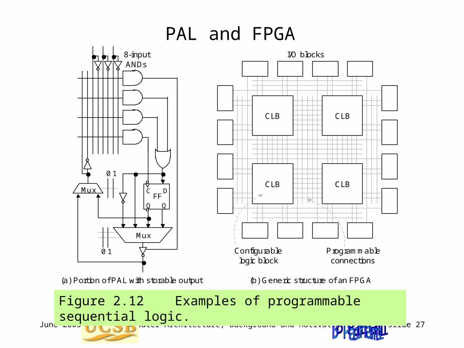
June 2005 Computer Architecture, Background and Motivation Slide 27
PAL and FPGA
Figure 2.12 Examples of programmable sequential logic.
(a) Portion of PAL with storable output (b) Generic structure of an FPGA
8-input ANDs
D
C Q
Q
FF
Mux
Mux
0 1
0 1
I/O blocks
Configurable logic block
Programmable connections
CLB
CLB
CLB
CLB
June 2005 Computer Architecture, Background and Motivation Slide 28
Binary Counter
Figure 2.11 Synchronous binary counter with initialization capability.
Count register
Mux
Incrementer
0
Input
Load
IncrInit
x + 1
x
0 1
1 c in c out
June 2005 Computer Architecture, Background and Motivation Slide 29
2.6 Clocks and Timing of Events
Clock is a periodic signal: clock rate = clock frequencyThe inverse of clock rate is the clock period: 1 GHz 1 ns
Constraint: Clock period tprop + tcomb + tsetup + tskew
Figure 2.13 Determining the required length of the clock period.
Other inputs
Combinational logic
Clock period
FF1 begins to change
FF1 change observed
Must be wide enough to accommodate
worst-case delays
Clock1 Clock2
Q C
Q
D
FF2
Q C
Q
D
FF1
June 2005 Computer Architecture, Background and Motivation Slide 30
Synchronization
Figure 2.14 Synchronizers are used to prevent timing problems
arising from untimely changes in asynchronous signals.
Asynch input
Asynch input
Synch version
Synch version
Asynch input
Synch version
Clock
(a) Simple synchronizer (b) Two-FF synchronizer
(c) Input and output waveforms
Q
C
Q
D
FF
Q
C
Q
D
FF2
Q
C
Q
D
FF1
June 2005 Computer Architecture, Background and Motivation Slide 31
Level-Sensitive Operation
Figure 2.15 Two-phase clocking with nonoverlapping clock signals.
Combi- national
logic 1 1
Clock period
Q C
Q
D
Latch
1
Q C
Q
D
Latch
Other inputs
Combi- national
logic 2
2
Clocks with nonoverlapping highs
Other inputs
Q C
Q
Latch
D
June 2005 Computer Architecture, Background and Motivation Slide 32
What Is (Computer) Architecture?
Figure 3.2 Like a building architect, whose place at the engineering/arts and goals/means interfaces is seen in this diagram, a
computer architect reconciles many conflicting or competing demands.
Architect Interface
Interface
Goals
Means
Arts Engineering
Client’s taste: mood, style, . . .
Client’s requirements: function, cost, . . .
The world of arts: aesthetics, trends, . . .
Construction technology: material, codes, . . .
June 2005 Computer Architecture, Background and Motivation Slide 33
3.2 Computer Systems and Their Parts
Figure 3.3 The space of computer systems, with what we normally mean by the word “computer” highlighted.
Computer
Analog
Fixed-function Stored-program
Electronic Nonelectronic
General-purpose Special-purpose
Number cruncher Data manipulator
Digital
June 2005 Computer Architecture, Background and Motivation Slide 34
Price/Performance Pyramid
Figure 3.4 Classifying computers by computational
power and price range.
Embedded Personal
Workstation
Server
Mainframe
Super $Millions $100s Ks
$10s Ks
$1000s
$100s
$10s
Differences in scale, not in substance
June 2005 Computer Architecture, Background and Motivation Slide 35
3.3 Generations of ProgressTable 3.2 The 5 generations of digital computers, and their ancestors.
Generation (begun)
Processor technology
Memory innovations
I/O devices introduced
Dominant look & fell
0 (1600s) (Electro-) mechanical
Wheel, card Lever, dial, punched card
Factory equipment
1 (1950s) Vacuum tube Magnetic drum
Paper tape, magnetic tape
Hall-size cabinet
2 (1960s) Transistor Magnetic core Drum, printer, text terminal
More abstract, machine-independent; easier to write, read, debug, or maintain
More concrete, machine-specific, error-prone; harder to write, read, debug, or maintain
June 2005 Computer Architecture, Background and Motivation Slide 39
4 Computer PerformancePerformance is key in design decisions; also cost and power
• It has been a driving force for innovation• Isn’t quite the same as speed (higher clock rate)
Topics in This Chapter
4.1 Cost, Performance, and Cost/Performance
4.2 Defining Computer Performance
4.3 Performance Enhancement and Amdahl’s Law
4.4 Performance Measurement vs Modeling
4.5 Reporting Computer Performance
4.6 The Quest for Higher Performance
June 2005 Computer Architecture, Background and Motivation Slide 40
4.1 Cost, Performance, and Cost/PerformanceTable 4.1 Key characteristics of six passenger aircraft: all figures are approximate; some relate to a specific model/configuration of the aircraft or are averages of cited range of values.
Aircraft PassengersRange
(km)Speed (km/h)
Price ($M)
Airbus A310 250 8 300 895 120
Boeing 747 470 6 700 980 200
Boeing 767 250 12 300 885 120
Boeing 777 375 7 450 980 180
Concorde 130 6 400 2 200 350
DC-8-50 145 14 000 875 80
June 2005 Computer Architecture, Background and Motivation Slide 41
The Vanishing Computer Cost
1980 1960 2000 2020 $1
Co
mp
ute
r co
st
Calendar year
$1 K
$1 M
$1 G
June 2005 Computer Architecture, Background and Motivation Slide 42
Figure 4.1 Performance improvement as a function of cost.
Cost/Performance
Performance
Cost
Superlinear: economy of scale
Sublinear: diminishing returns
Linear (ideal?)
June 2005 Computer Architecture, Background and Motivation Slide 43
4.2 Defining Computer Performance
Figure 4.2 Pipeline analogy shows that imbalance between processing power and I/O capabilities leads to a performance bottleneck.
Processing Input Output
CPU-bound task
I/O-bound task
June 2005 Computer Architecture, Background and Motivation Slide 44
Different Views of performance
Performance from the viewpoint of a passenger: Speed
Note, however, that flight time is but one part of total travel time. Also, if the travel distance exceeds the range of a faster plane, a slower plane may be better due to not needing a refueling stop
Performance from the viewpoint of an airline: Throughput
Measured in passenger-km per hour (relevant if ticket price were proportional to distance traveled, which in reality is not)
Airbus A310 250 895 = 0.224 M passenger-km/hr Boeing 747 470 980 = 0.461 M passenger-km/hr Boeing 767 250 885 = 0.221 M passenger-km/hr Boeing 777 375 980 = 0.368 M passenger-km/hr Concorde 130 2200 = 0.286 M passenger-km/hr DC-8-50 145 875 = 0.127 M passenger-km/hr
Performance from the viewpoint of FAA: Safety
June 2005 Computer Architecture, Background and Motivation Slide 45
Cost Effectiveness: Cost/Performance
Table 4.1 Key characteristics of six passenger aircraft: all figures are approximate; some relate to a specific model/configuration of the aircraft or are averages of cited range of values.
Aircraft Passen-gers
Range (km)
Speed (km/h)
Price ($M)
A310 250 8 300 895 120
B 747 470 6 700 980 200
B 767 250 12 300 885 120
B 777 375 7 450 980 180
Concorde 130 6 400 2 200 350
DC-8-50 145 14 000 875 80
Cost / Performance
536
434
543
489
1224
630
Throughput(M P km/hr)
0.224
0.461
0.221
0.368
0.286
0.127
Smallervaluesbetter
Largervaluesbetter
June 2005 Computer Architecture, Background and Motivation Slide 46
Concepts of Performance and Speedup
Performance = 1 / Execution time is simplified to
Performance = 1 / CPU execution time
(Performance of M1) / (Performance of M2) = Speedup of M1 over M2
= (Execution time of M2) / (Execution time M1)
Terminology: M1 is x times as fast as M2 (e.g., 1.5 times as fast)
M1 is 100(x – 1)% faster than M2 (e.g., 50% faster)
CPU time = Instructions (Cycles per instruction) (Secs per cycle)
= Instructions CPI / (Clock rate)
Instruction count, CPI, and clock rate are not completely independent, so improving one by a given factor may not lead to overall execution time improvement by the same factor.
June 2005 Computer Architecture, Background and Motivation Slide 47
Figure 4.3 Faster steps do not necessarily mean shorter travel time.
Faster Clock Shorter Running Time
1 GHz
2 GHz
4 steps
Solution
20 steps
June 2005 Computer Architecture, Background and Motivation Slide 48
0
10
20
30
40
50
0 10 20 30 40 50Enhancement factor (p )
Spe
edup
(s
)
f = 0
f = 0.1
f = 0.05
f = 0.02
f = 0.01
4.3 Performance Enhancement: Amdahl’s Law
Figure 4.4 Amdahl’s law: speedup achieved if a fraction f of a task is unaffected and the remaining 1 – f part runs p times as fast.
s =
min(p, 1/f)
1f + (1 – f)/p
f = fraction unaffected
p = speedup of the rest
June 2005 Computer Architecture, Background and Motivation Slide 49
Example 4.1
Amdahl’s Law Used in Design
A processor spends 30% of its time on flp addition, 25% on flp mult, and 10% on flp division. Evaluate the following enhancements, each costing the same to implement:
a. Redesign of the flp adder to make it twice as fast.b. Redesign of the flp multiplier to make it three times as fast.c. Redesign the flp divider to make it 10 times as fast.
What if both the adder and the multiplier are redesigned?
June 2005 Computer Architecture, Background and Motivation Slide 50
4.4 Performance Measurement vs. Modeling
Figure 4.5 Running times of six programs on three machines.
Execution time
Program
A E F B C D
Machine 1
Machine 2
Machine 3
June 2005 Computer Architecture, Background and Motivation Slide 51
MIPS Rating Can Be Misleading
Example 4.5
Two compilers produce machine code for a program on a machine with two classes of instructions. Here are the number of instructions:
Class CPI Compiler 1 Compiler 2 A 1 600M 400M B 2 400M 400M
a. What are run times of the two programs with a 1 GHz clock?b. Which compiler produces faster code and by what factor? c. Which compiler’s output runs at a higher MIPS rate?
Solution
a. Running time 1 (2) = (600M 1 + 400M 2) / 109 = 1.4 s (1.2 s)
b. Compiler 2’s output runs 1.4 / 1.2 = 1.17 times as fastc. MIPS rating 1, CPI = 1.4 (2, CPI = 1.5) = 1000 / 1.4 = 714 (667)
June 2005 Computer Architecture, Background and Motivation Slide 52
4.5 Reporting Computer Performance
Table 4.4 Measured or estimated execution times for three programs.
Time on machine X
Time on machine Y
Speedup of Y over X
Program A 20 200 0.1
Program B 1000 100 10.0
Program C 1500 150 10.0
All 3 prog’s 2520 450 5.6
Analogy: If a car is driven to a city 100 km away at 100 km/hr and returns at 50 km/hr, the average speed is not (100 + 50) / 2 but is obtained from the fact that it travels 200 km in 3 hours.
June 2005 Computer Architecture, Background and Motivation Slide 53
Table 4.4 Measured or estimated execution times for three programs.
Time on machine X
Time on machine Y
Speedup of Y over X
Program A 20 200 0.1
Program B 1000 100 10.0
Program C 1500 150 10.0
Geometric mean does not yield a measure of overall speedup, but provides an indicator that at least moves in the right direction
Comparing the Overall Performance
Speedup of X over Y
10
0.1
0.1
Arithmetic meanGeometric mean
6.72.15
3.40.46
June 2005 Computer Architecture, Background and Motivation Slide 54
4.6 The Quest for Higher PerformanceState of available computing power ca. the early 2000s:
Gigaflops on the desktopTeraflops in the supercomputer centerPetaflops on the drawing board
Note on terminology (see Table 3.1)
Prefixes for large units:Kilo = 103, Mega = 106, Giga = 109, Tera = 1012, Peta = 1015
For memory:K = 210 = 1024, M = 220, G = 230, T = 240, P = 250
Prefixes for small units:micro = 106, nano = 109, pico = 1012, femto = 1015
June 2005 Computer Architecture, Background and Motivation Slide 55
Figure 4.7 Exponential growth of supercomputer performance.
Supercom-puters
1990 1980 2000 2010
Sup
erc
om
put
er
pe
rfo
rma
nce
Calendar year
Cray X-MP
Y-MP
CM-2
MFLOPS
GFLOPS
TFLOPS
PFLOPS
Vector supercomputers
CM-5
CM-5
$240M MPPs
$30M MPPs
Massively parallel processors
June 2005 Computer Architecture, Background and Motivation Slide 56
Figure 4.8 Milestones in the DOE’s Accelerated Strategic Computing Initiative (ASCI) program with extrapolation up to the PFLOPS level.
The Most Powerful Computers
2000 1995 2005 2010
Pe
rfo
rma
nce
(T
FL
OP
S)
Calendar year
ASCI Red
ASCI Blue
ASCI White
1+ TFLOPS, 0.5 TB
3+ TFLOPS, 1.5 TB
10+ TFLOPS, 5 TB
30+ TFLOPS, 10 TB
100+ TFLOPS, 20 TB
1
10
100
1000 Plan Develop Use
ASCI
ASCI Purple
ASCI Q
June 2005 Computer Architecture, Background and Motivation Slide 57
Figure 25.1 Trend in energy consumption per MIPS of computational power in general-purpose processors and DSPs.