1 K9F1G08U0A K9F1G08R0A K9K2G08U1A FLASH MEMORY K9F1G08X0A * Samsung Electronics reserves the right to change products or specification without notice. INFORMATION IN THIS DOCUMENT IS PROVIDED IN RELATION TO SAMSUNG PRODUCTS, AND IS SUBJECT TO CHANGE WITHOUT NOTICE. NOTHING IN THIS DOCUMENT SHALL BE CONSTRUED AS GRANTING ANY LICENSE, EXPRESS OR IMPLIED, BY ESTOPPEL OR OTHERWISE, TO ANY INTELLECTUAL PROPERTY RIGHTS IN SAMSUNG PRODUCTS OR TECHNOLOGY. ALL INFORMATION IN THIS DOCUMENT IS PROVIDED ON AS "AS IS" BASIS WITHOUT GUARANTEE OR WARRANTY OF ANY KIND. 1. For updates or additional information about Samsung products, contact your nearest Samsung office. 2. Samsung products are not intended for use in life support, critical care, medical, safety equipment, or similar applications where Product failure could result in loss of life or personal or physical harm, or any military or defense application, or any governmental procurement to which special terms or provisions may apply.
Transcript
1
K9F1G08U0AK9F1G08R0A
K9K2G08U1A FLASH MEMORY
K9F1G08X0A
* Samsung Electronics reserves the right to change products or specification without notice.
INFORMATION IN THIS DOCUMENT IS PROVIDED IN RELATION TO SAMSUNG PRODUCTS,AND IS SUBJECT TO CHANGE WITHOUT NOTICE.
NOTHING IN THIS DOCUMENT SHALL BE CONSTRUED AS GRANTING ANY LICENSE,EXPRESS OR IMPLIED, BY ESTOPPEL OR OTHERWISE,
TO ANY INTELLECTUAL PROPERTY RIGHTS IN SAMSUNG PRODUCTS OR TECHNOLOGY. ALLINFORMATION IN THIS DOCUMENT IS PROVIDED
ON AS "AS IS" BASIS WITHOUT GUARANTEE OR WARRANTY OF ANY KIND.
1. For updates or additional information about Samsung products, contact your nearest Samsung office.
2. Samsung products are not intended for use in life support, critical care, medical, safety equipment, or similarapplications where Product failure could result in loss of life or personal or physical harm, or any military ordefense application, or any governmental procurement to which special terms or provisions may apply.
2
K9F1G08U0AK9F1G08R0A
K9K2G08U1A FLASH MEMORY
Document Title128M x 8 Bit / 256M x 8 Bit NAND Flash Memory
Revision History
The attached data sheets are prepared and approved by SAMSUNG Electronics. SAMSUNG Electronics CO., LTD. reserve the rightto change the specifications. SAMSUNG Electronics will evaluate and reply to your requests and questions about device. If you haveany questions, please contact the SAMSUNG branch office near your office.
Revision No
0.00.1
0.2
0.3
0.4
0.5
0.6
0.7
0.8
1.0
Remark
AdvancePreliminary
Preliminary
Preliminary
Preliminary
Preliminary
History
1. Initial issue1. The tADL(Address to Data Loading Time) is added. - tADL Minimum 100ns (Page 11, 23~26) - tADL is the time from the WE rising edge of final address cycle to the WE rising edge of first data cycle at program operation.
2. Added Addressing method for program operation
1. Add the Protrusion/Burr value in WSOP1 PKG Diagram.
1. PKG(TSOP1, WSOP1) Dimension Change
1. Technical note is changed2. Notes of AC timing characteristics are added3. The description of Copy-back program is changed 4. Voltage range is changed -1.7V~1.95V -> 1.65V~1.95V5. Note2 of Command Sets is added
1. CE access time : 23ns->35ns (p.11)
1. The value of tREA for 3.3V device is changed.(18ns->20ns)2. EDO mode is added.
1. The flow chart to creat the initial invalid block table is cahnged.
1. 1.8V FBGA package is added
1. 3.3V FBGA package is added
Draft Date
Aug. 24. 2003Jan. 27. 2004
Apr. 23. 2004
May. 19. 2004
Jan. 21. 2005
Feb. 14. 2005
May. 4. 2005
May 6. 2005
Aug. 5. 2005
Jan. 27. 2006
3
K9F1G08U0AK9F1G08R0A
K9K2G08U1A FLASH MEMORY
GENERAL DESCRIPTION
FEATURES• Voltage Supply -1.8V device(K9F1G08R0A): 1.65V~1.95V -3.3V device(K9F1G08U0A): 2.7 V ~3.6 V• Organization - Memory Cell Array : (128M + 4,096K)bit x 8bit - Data Register : (2K + 64)bit x8bit - Cache Register : (2K + 64)bit x8bit • Automatic Program and Erase - Page Program : (2K + 64)Byte - Block Erase : (128K + 4K)Byte• Page Read Operation - Page Size : 2K-Byte - Random Read : 25µs(Max.) - Serial Access : 30ns(Min.) - 3.3v device 50ns(Min.) -1.8v device
128M x 8 Bit /256M x 8 Bit NAND Flash Memory
• Fast Write Cycle Time - Program time : 200µs(Typ.) - Block Erase Time : 2ms(Typ.)• Command/Address/Data Multiplexed I/O Port• Hardware Data Protection - Program/Erase Lockout During Power Transitions• Reliable CMOS Floating-Gate Technology - Endurance : 100K Program/Erase Cycles - Data Retention : 10 Years• Command Register Operation• Cache Program Operation for High Performance Program• Intelligent Copy-Back Operation• Unique ID for Copyright Protection• Package : - K9F1G08X0A-JCB0/JIB0 63- Ball FBGA (9.5 x 12) - Pb-free Package - K9F1G08U0A-PCB0/PIB0 48 - Pin TSOP I (12 x 20 / 0.5 mm pitch)- Pb-free Package - K9F1G08U0A-FIB0 48 - Pin WSOP I (12X17X0.7mm)- Pb-free Package * K9F1G08U0A-F(WSOPI ) is the same device as K9F1G08U0A-P(TSOP1) except package type. - K9K2G08U1A-ICB0/IIB0 52-ULGA (12X17X0.65mm)
Offered in 128Mx8bit the K9F1G08X0A is 1G bit with spare 32M bit capacity. Its NAND cell provides the most cost-effective solutionfor the solid state mass storage market. A program operation can be performed in typical 200µs on the 2112-byte page and an eraseoperation can be performed in typical 2ms on a 128K-byte block. Data in the data page can be read out at 30ns(50ns with 1.8Vdevice) cycle time per byte. The I/O pins serve as the ports for address and data input/output as well as command input. The on-chipwrite controller automates all program and erase functions including pulse repetition, where required, and internal verification andmargining of data. Even the write-intensive systems can take advantage of the K9F1G08X0A′s extended reliability of 100K program/erase cycles by providing ECC(Error Correcting Code) with real time mapping-out algorithm. The K9F1G08X0A is an optimum solu-tion for large nonvolatile storage applications such as solid state file storage and other portable applications requiring non-volatility.
PRODUCT LISTPart Number Vcc Range Organization PKG Type
K9F1G08R0A-J 1.65 ~ 1.95V
X8
FBGA
K9F1G08U0A-P
2.7 ~ 3.6V
TSOP1
K9F1G08U0A-F WSOP1
K9F1G08U0A-J FBGA
K9K2G08U1A-I 52-ULGA
4
K9F1G08U0AK9F1G08R0A
K9K2G08U1A FLASH MEMORY
PIN CONFIGURATION (TSOP1)K9F1G08U0A-PCB0/PIB0
PACKAGE DIMENSIONS
48-PIN LEAD/LEAD FREE PLASTIC THIN SMALL OUT-LINE PACKAGE TYPE(I)
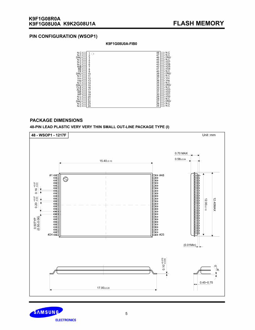
PACKAGE DIMENSIONS48-PIN LEAD PLASTIC VERY VERY THIN SMALL OUT-LINE PACKAGE TYPE (I)
48 - WSOP1 - 1217F Unit :mm
15.40±0.10
#1
#24
0.20
+0.0
7-0
.03
0.16
+0.0
7-0
.03
0.50
TYP
(0.5
0±0.
06)
#48
#25
0.10
+0.0
75-0
.035
17.00±0.20
0°~8°
0.45~0.75
12.00±0.10
0.58±0.04
0.70 MAX
(0.01Min)
12.40MAX
6
K9F1G08U0AK9F1G08R0A
K9K2G08U1A FLASH MEMORY
K9F1G08X0A-JCB0/JIB0
PIN CONFIGURATION (FBGA)
R/B/WE/CEVssALE/WP
/RE CLE
NCNC
NC NC VccNCNC I/O0
I/O1NC NC Vcc I/O5 I/O7
VssI/O6I/O4I/O3I/O2Vss
NC
NC
NC
NC NC
NC
NC NC
NC
NC
NC
NC
NC NC NC
NC
NC
NC
NC
NC
N.C
N.C N.C
N.C
N.C N.C
N.C
N.C
N.C N.C
N.CN.C
N.C N.C
N.C
3 4 5 6 1 2
AB
C
D
G
E
F
H
Top View
7
K9F1G08U0AK9F1G08R0A
K9K2G08U1A FLASH MEMORY
9.50±0.10
#A1
Side View
Top View
1.20
(Max
)
0.45±0.05
Bottom View
12.0
0±0.
10
63-∅0.45±0.05
0.25
(Min
.)
0.10MAX
0.20 M A B ∅
12.00±0.10
4 3 2 1
A
B
C
D
G
0.80
x 7
= 5
.60
12.0
0±0.
10
0.80 x 5= 4.00 0.80 B
A
2.80
2.00
9.50±0.10
(Datum B)
(Datum A)
0.80
0.80
x 1
1= 8
.80
0.80 x 9= 7.20
6 5
E
F
H
#A1 INDEX MARK(OPTIONAL)
PACKAGE DEMENSIONS(FBGA)
8
K9F1G08U0AK9F1G08R0A
K9K2G08U1A FLASH MEMORYPIN CONFIGURATION (ULGA)
1.00
1.001.00
1.00
2.00
7 6 5 4 3 2 1
1.00
1.00
1.00
12.00±0.10
#A1
17.0
0±0.
10
17.0
0±0.
10
B
A12.00±0.10
(Datum B)
(Datum A)
12.0
0
10.00
2.50
2.50
2.00
0.50
1.30
A
B
C
D
E
F
G
H
J
K
L
M
N
12-∅1.00±0.05 41-∅0.70±0.05
Side View
0.65
(Max.)
0.10 C
17.00±0.10
Top View Bottom View
A B C D E F G H J K L M N
7
6
5
4
3
2
1
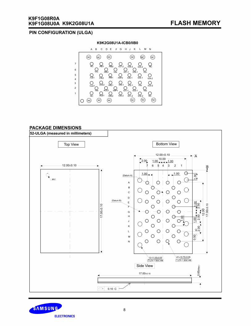
K9K2G08U1A-ICB0/IIB0
52-ULGA (measured in millimeters)
NC NC NC NC NC NC
NC NC NCNCNCNC
NC
NCNC
NC
VccVcc
Vss
Vss
Vss
/RE1
/RE2
/CE1 /CE2
CLE1 CLE2
ALE1
ALE2
/WE1
/WE2
/WP1
/WP2/RB1
/RB2
Vss
IO0-1
IO0-2
IO1-1
IO1-2
IO2-1
IO3-1
IO2-2
IO3-2
IO4-1 IO4-2
IO5-1
IO5-2
IO6-1
IO6-2
IO7-1
IO7-2
∅ ABCM0.1 ∅ ABCM0.1
PACKAGE DIMENSIONS
9
K9F1G08U0AK9F1G08R0A
K9K2G08U1A FLASH MEMORY
PIN DESCRIPTION
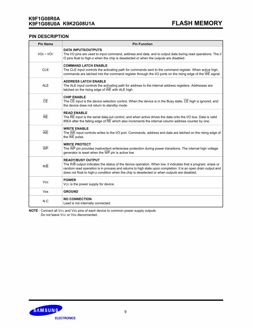
NOTE : Connect all VCC and VSS pins of each device to common power supply outputs. Do not leave VCC or VSS disconnected.
Pin Name Pin Function
I/O0 ~ I/O7
DATA INPUTS/OUTPUTS The I/O pins are used to input command, address and data, and to output data during read operations. The I/O pins float to high-z when the chip is deselected or when the outputs are disabled.
CLECOMMAND LATCH ENABLEThe CLE input controls the activating path for commands sent to the command register. When active high, commands are latched into the command register through the I/O ports on the rising edge of the WE signal.
ALEADDRESS LATCH ENABLEThe ALE input controls the activating path for address to the internal address registers. Addresses are latched on the rising edge of WE with ALE high.
CECHIP ENABLEThe CE input is the device selection control. When the device is in the Busy state, CE high is ignored, and the device does not return to standby mode.
REREAD ENABLEThe RE input is the serial data-out control, and when active drives the data onto the I/O bus. Data is valid tREA after the falling edge of RE which also increments the internal column address counter by one.
WEWRITE ENABLEThe WE input controls writes to the I/O port. Commands, address and data are latched on the rising edge of the WE pulse.
WPWRITE PROTECTThe WP pin provides inadvertent write/erase protection during power transitions. The internal high voltage generator is reset when the WP pin is active low.
R/B
READY/BUSY OUTPUTThe R/B output indicates the status of the device operation. When low, it indicates that a program, erase or random read operation is in process and returns to high state upon completion. It is an open drain output and does not float to high-z condition when the chip is deselected or when outputs are disabled.
Vcc POWERVCC is the power supply for device.
Vss GROUND
N.C NO CONNECTIONLead is not internally connected.
10
K9F1G08U0AK9F1G08R0A
K9K2G08U1A FLASH MEMORY
2K Bytes 64 Bytes
Figure 1-1. K9F1G08X0A Functional Block Diagram
Figure 2-1. K9F1G08X0A Array Organization
NOTE : Column Address : Starting Address of the Register.* L must be set to "Low".* The device ignores any additional input of address cycles than required.
I/O 0 I/O 1 I/O 2 I/O 3 I/O 4 I/O 5 I/O 6 I/O 7
1st Cycle A0 A1 A2 A3 A4 A5 A6 A7
2nd Cycle A8 A9 A10 A11 *L *L *L *L
3rd Cycle A12 A13 A14 A15 A16 A17 A18 A19
4th Cycle A20 A21 A22 A23 A24 A25 A26 A27
VCC
X-Buffers
Command
I/O Buffers & Latches
Latches& Decoders
Y-BuffersLatches& Decoders
Register
Control Logic& High Voltage
Generator Global Buffers OutputDriver
VSS
A12 - A27
A0 - A11
Command
CEREWE
CLE WP
I/0 0
I/0 7
VCCVSS
64K Pages(=1,024 Blocks)
2K Bytes
8 bit
64 Bytes
1 Block = 64 Pages(128K + 4k) Byte
I/O 0 ~ I/O 7
1 Page = (2K + 64)Bytes1 Block = (2K + 64)B x 64 Pages = (128K + 4K) Bytes1 Device = (2K+64)B x 64Pages x 1024 Blocks = 1056 Mbits
Row Address
Page Register
ALE PRE
1024M + 32M BitNAND Flash
ARRAY
(2048 + 64)Byte x 65536
Y-GatingCache Register
Row Address
Column Address
Column Address
Data Register & S/A
11
K9F1G08U0AK9F1G08R0A
K9K2G08U1A FLASH MEMORY
Product IntroductionThe K9F1G08X0A is a 1056Mbit(1,107,296,256 bit) memory organized as 65,536 rows(pages) by 2112x8 columns. Spare 64 col-umns are located from column address of 2048~2111. A 2112-byte data register and a 2112-byte cache register are serially con-nected to each other. Those serially connected registers are connected to memory cell arrays for accommodating data transferbetween the I/O buffers and memory cells during page read and page program operations. The memory array is made up of 32 cellsthat are serially connected to form a NAND structure. Each of the 32 cells resides in a different page. A block consists of two NANDstructured strings. A NAND structure consists of 32 cells. Total 1081344 NAND cells reside in a block. The program and read opera-tions are executed on a page basis, while the erase operation is executed on a block basis. The memory array consists of 1024 sep-arately erasable 128K-byte blocks. It indicates that the bit by bit erase operation is prohibited on the K9F1G08X0A.
The K9F1G08X0A has addresses multiplexed into 8 I/Os. This scheme dramatically reduces pin counts and allows system upgradesto future densities by maintaining consistency in system board design. Command, address and data are all written through I/O's bybringing WE to low while CE is low. Those are latched on the rising edge of WE. Command Latch Enable(CLE) and Address LatchEnable(ALE) are used to multiplex command and address respectively, via the I/O pins. Some commands require one bus cycle. Forexample, Reset Command, Status Read Command, etc require just one cycle bus. Some other commands, like page read and blockerase and page program, require two cycles: one cycle for setup and the other cycle for execution. The 132M byte physical spacerequires 28 addresses, thereby requiring four cycles for addressing: 2 cycles of column address, 2 cycles of row address, in thatorder. Page Read and Page Program need the same four address cycles following the required command input. In Block Erase oper-ation, however, only the two row address cycles are used. Device operations are selected by writing specific commands into the com-mand register. Table 1 defines the specific commands of the K9F1G08X0A.
The device provides cache program in a block. It is possible to write data into the cache registers while data stored in data registersare being programmed into memory cells in cache program mode. The program performace may be dramatically improved by cacheprogram when there are lots of pages of data to be programmed.
In addition to the enhanced architecture and interface, the device incorporates copy-back program feature from one page to anotherpage without need for transporting the data to and from the external buffer memory. Since the time-consuming serial access anddata-input cycles are removed, system performance for solid-state disk application is significantly increased.
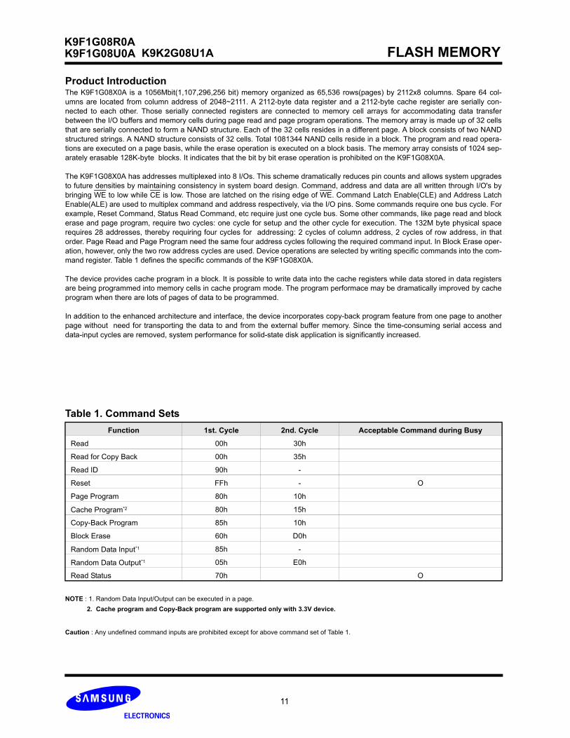
Table 1. Command Sets
NOTE : 1. Random Data Input/Output can be executed in a page. 2. Cache program and Copy-Back program are supported only with 3.3V device.
Function 1st. Cycle 2nd. Cycle Acceptable Command during Busy
Read 00h 30h
Read for Copy Back 00h 35h
Read ID 90h -
Reset FFh - O
Page Program 80h 10h
Cache Program*2 80h 15h
Copy-Back Program 85h 10h
Block Erase 60h D0h
Random Data Input*1 85h -
Random Data Output*1 05h E0h
Read Status 70h O
Caution : Any undefined command inputs are prohibited except for above command set of Table 1.
12
K9F1G08U0AK9F1G08R0A
K9K2G08U1A FLASH MEMORY
RECOMMENDED OPERATING CONDITIONS(Voltage reference to GND, K9F1G08X0A-XCB0 :TA=0 to 70°C, K9F1G08X0A-XIB0:TA=-40 to 85°C)
Parameter SymbolK9F1G08R0A(1.8V) K9F1G08U0A(3.3V)
UnitMin Typ. Max Min Typ. Max
Supply Voltage VCC 1.65 1.8 1.95 2.7 3.3 3.6 V
Supply Voltage VSS 0 0 0 0 0 0 V
ABSOLUTE MAXIMUM RATINGS
NOTE : 1. Minimum DC voltage is -0.6V on input/output pins. During transitions, this level may undershoot to -2.0V for periods <30ns. Maximum DC voltage on input/output pins is VCC,+0.3V which, during transitions, may overshoot to VCC+2.0V for periods <20ns.2. Permanent device damage may occur if ABSOLUTE MAXIMUM RATINGS are exceeded. Functional operation should be restricted to the conditions as detailed in the operational sections of this data sheet. Exposure to absolute maximum rating conditions for extended periods may affect reliability.
Parameter SymbolRating
Unit1.8V DEVICE 3.3V DEVICE
Voltage on any pin relative to VSSVIN/OUT -0.6 to + 2.45 -0.6 to + 4.6
VVCC -0.2 to + 2.45 -0.6 to + 4.6
Temperature Under Bias
K9F1G08X0A-XCB0TBIAS
-10 to +125°C
K9F1G08X0A-XIB0 -40 to +125
Storage TemperatureK9F1G08X0A-XCB0
TSTG -65 to +150 °CK9F1G08X0A-XIB0
Short Circuit Current Ios 5 mA
DC AND OPERATING CHARACTERISTICS(Recommended operating conditions otherwise noted.)
NOTE : VIL can undershoot to -0.4V and VIH can overshoot to VCC +0.4V for durations of 20 ns or less.
NOTE : Capacitance is periodically sampled and not 100% tested.
Item Symbol Test Condition Min Max Unit
Input/Output Capacitance CI/O VIL=0V - 10 pF
Input Capacitance CIN VIN=0V - 10 pF
VALID BLOCK
NOTE : 1. The K9F1G08X0A may include invalid blocks when first shipped. Additional invalid blocks may develop while being used. The number of valid
blocks is presented with both cases of invalid blocks considered. Invalid blocks are defined as blocks that contain one or more bad bits. Do not eraseor program factory-marked bad blocks. Refer to the attached technical notes for appropriate management of invalid blocks.
2. The 1st block, which is placed on 00h block address, is guaranteed to be a valid block, does not require Error Correction up to 1K program/erasecycles.
* : Each K9F1G08U0A chip in the K9K2G08U1A has Maximum 20 invalid blocks.
Parameter Symbol Min Typ. Max Unit
K9F1G08X0A NVB 1004 - 1024 Blocks
K9K2G08U1A NVB 2008 - 2048 Blocks
AC TEST CONDITION(K9F1G08X0A-XCB0 :TA=0 to 70°C, K9F1G08X0A-XIB0:TA=-40 to 85°C
Output Load 1 TTL GATE and CL=30pF 1 TTL GATE and CL=50pF
MODE SELECTION
NOTE : 1. X can be VIL or VIH.
2. WP should be biased to CMOS high or CMOS low for standby.
CLE ALE CE WE RE WP Mode
H L L H XRead Mode
Command Input
L H L H X Address Input(4clock)
H L L H HWrite Mode
Command Input
L H L H H Address Input(4clock)
L L L H H Data Input
L L L H X Data Output
X X X X H X During Read(Busy)
X X X X X H During Program(Busy)
X X X X X H During Erase(Busy)
X X*1 X X X L Write Protect
X X H X X 0V/VCC(2) Stand-by
Program / Erase Characteristics
NOTE : 1. Typical program time is defined as the time within which more than 50% of the whole pages are programmed at Vcc of 3.3V ans 25’C. 2. Max. time of tCBSY depends on timing between internal program completion and data in.
Parameter Symbol Min Typ Max Unit
Program Time tPROG*1 - 200 700 µs
Dummy Busy Time for Cache Program tCBSY*2 3 700 µs
Number of Partial Program Cyclesin the Same Page
Main ArrayNop
- - 4 cycles
Spare Array - - 4 cycles
Block Erase Time tBERS - 2 3 ms
14
K9F1G08U0AK9F1G08R0A
K9K2G08U1A FLASH MEMORY
AC Timing Characteristics for Command / Address / Data Input
NOTE : 1. The transition of the corresponding control pins must occur only once while WE is held low. 2. tADL is the time from the WE rising edge of final address cycle to the WE rising edge of first data cycle. 3. For cache program operation, the whole AC Charcateristics must be same as that of K9F1G08R0A.
Parameter SymbolMin Max
UnitK9F1G08R0A K9F1G08U0A K9F1G08R0A K9F1G08U0A
CLE setup Time tCLS*1 25 15 - - ns
CLE Hold Time tCLH 10 5 - - ns
CE setup Time tCS*1 35 20 - - ns
CE Hold Time tCH 10 5 - - ns
WE Pulse Width tWP 25 15 - - ns
ALE setup Time tALS*1 25 15 - - ns
ALE Hold Time tALH 10 5 - - ns
Data setup Time tDS*1 20 15 - - ns
Data Hold Time tDH 10 5 - - ns
Write Cycle Time tWC 45 30 - - ns
WE High Hold Time tWH 15 10 - - ns
ALE to Data Loading Time tADL*2 100*2 100*2 - - ns
AC Characteristics for Operation
NOTE: 1. If reset command(FFh) is written at Ready state, the device goes into Busy for maximum 5us. 2. For cache program operation, the whole AC Charcateristics must be same as that of K9F1G08R0A.
Parameter SymbolMin Max
UnitK9F1G08R0A K9F1G08U0A K9F1G08R0A K9F1G08U0A
Data Transfer from Cell to Register tR - - 25 25 µs
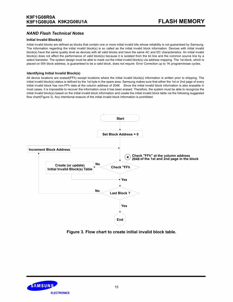
Initial Invalid Block(s)Initial invalid blocks are defined as blocks that contain one or more initial invalid bits whose reliability is not guaranteed by Samsung.The information regarding the initial invalid block(s) is so called as the initial invalid block information. Devices with initial invalidblock(s) have the same quality level as devices with all valid blocks and have the same AC and DC characteristics. An initial invalidblock(s) does not affect the performance of valid block(s) because it is isolated from the bit line and the common source line by aselect transistor. The system design must be able to mask out the initial invalid block(s) via address mapping. The 1st block, which isplaced on 00h block address, is guaranteed to be a valid block, does not require Error Correction up to 1K program/erase cycles.
All device locations are erased(FFh) except locations where the initial invalid block(s) information is written prior to shipping. Theinitial invalid block(s) status is defined by the 1st byte in the spare area. Samsung makes sure that either the 1st or 2nd page of everyinitial invalid block has non-FFh data at the column address of 2048. Since the initial invalid block information is also erasable inmost cases, it is impossible to recover the information once it has been erased. Therefore, the system must be able to recognize theinitial invalid block(s) based on the initial invalid block information and create the initial invalid block table via the following suggestedflow chart(Figure 3). Any intentional erasure of the initial invalid block information is prohibited.
* Check "FFh" at the column address
Figure 3. Flow chart to create initial invalid block table.
Error in write or read operationWithin its life time, additional invalid blocks may develop with NAND Flash memory. Refer to the qualification report for the blockfailure rate.The following possible failure modes should be considered to implement a highly reliable system. In the case of statusread failure after erase or program, block replacement should be done. Because program status fail during a page program does notaffect the data of the other pages in the same block, block replacement can be executed with a page-sized buffer by finding anerased empty block and reprogramming the current target data and copying the rest of the replaced block.In case of Read, ECC mustbe employed. To improve the efficiency of memory space, it is recommended that the read failure due to single bit error should bereclaimed by ECC without any block replacement. The block failure rate in the qualification report does not include those reclaimedblocks.
Failure Mode Detection and Countermeasure sequence
Write Erase Failure Status Read after Erase --> Block Replacement
Program Failure Status Read after Program --> Block Replacement
Read Single Bit Failure Verify ECC -> ECC Correction
: If program operation results in an error, map outthe block including the page in error and copy the *target data to another block.
17
K9F1G08U0AK9F1G08R0A
K9K2G08U1A FLASH MEMORY
Erase Flow Chart
Start
I/O 6 = 1 ?
I/O 0 = 0 ? No*
Write 60h
Write Block Address
Write D0h
Read Status Register
or R/B = 1 ?
Erase Error
Yes
No
: If erase operation results in an error, map outthe failing block and replace it with another block. *
Erase Completed
Yes
Read Flow Chart
Start
Verify ECC No
Write 00h
Write Address
Read Data
ECC Generation
Reclaim the Error
Page Read Completed
Yes
NAND Flash Technical Notes (Continued)
Write 30h
Block Replacement
Buffer memory of the controller.
1stBlock A
Block B
(n-1)thnth
(page)
{∼
1st
(n-1)thnth
(page)
{∼
an error occurs.1
2
* Step1When an error happens in the nth page of the Block ’A’ during erase or program operation. * Step2Copy the data in the 1st ~ (n-1)th page to the same location of another free block. (Block ’B’)* Step3Then, copy the nth page data of the Block ’A’ in the buffer memory to the nth page of the Block ’B’.* Step4Do not erase or program to Block ’A’ by creating an ’invalid Block’ table or other appropriate scheme.
18
K9F1G08U0AK9F1G08R0A
K9K2G08U1A FLASH MEMORY
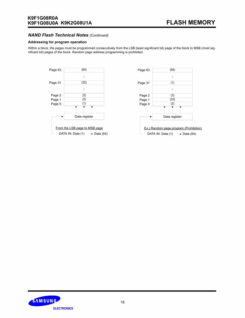
Within a block, the pages must be programmed consecutively from the LSB (least significant bit) page of the block to MSB (most sig-nificant bit) pages of the block. Random page address programming is prohibited.
From the LSB page to MSB page
DATA IN: Data (1) Data (64)
(1)(2)(3)
(32)
(64)
Data register
Page 0Page 1Page 2
Page 31
Page 63
Ex.) Random page program (Prohibition)
DATA IN: Data (1) Data (64)
(2)(32)(3)
(1)
(64)
Data register
Page 0Page 1Page 2
Page 31
Page 63
NAND Flash Technical Notes (Continued)Addressing for program operation
:
:
:
:
19
K9F1G08U0AK9F1G08R0A
K9K2G08U1A FLASH MEMORY
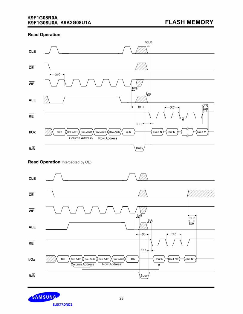
System Interface Using CE don’t-care. For an easier system interface, CE may be inactive during the data-loading or serial access as shown below. The internal 2112bytedata registers are utilized as separate buffers for this operation and the system design gets more flexible. In addition, for voice oraudio applications which use slow cycle time on the order of u-seconds, de-activating CE during the data-loading and serial accesswould provide significant savings in power consumption.
Device OperationPAGE READPage read is initiated by writing 00h-30h to the command register along with five address cycles. After initial power up, 00h commandis latched. Therefore only five address cycles and 30h command initiates that operation after initial power up. The 2,112 bytes of datawithin the selected page are transferred to the data registers in less than 25µs(tR). The system controller can detect the completion ofthis data transfer(tR) by analyzing the output of R/B pin. Once the data in a page is loaded into the data registers, they may be readout in 30ns cycle time(50ns with 1.8V device) by sequentially pulsing RE. The repetitive high to low transitions of the RE clock makethe device output the data starting from the selected column address up to the last column address. The device may output random data in a page instead of the consecutive sequential data by writing random data output command.The column address of next data, which is going to be out, may be changed to the address which follows random data output com-mand. Random data output can be operated multiple times regardless of how many times it is done in a page.
Figure 6. Read Operation
Address(4Cycle)00h
Col Add1,2 & Row Add1,2
Data Output(Serial Access)
Data Field Spare Field
CE
CLE
ALE
R/B
WE
RE
tR
30hI/Ox
33
K9F1G08U0AK9F1G08R0A
K9K2G08U1A FLASH MEMORY
Figure 7. Random Data Output In a Page
Address00h Data Output
R/B
RE
tR
30h Address05h E0h4Cycles 2Cycles Data Output
Data Field Spare Field Data Field Spare Field
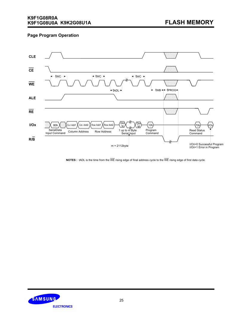
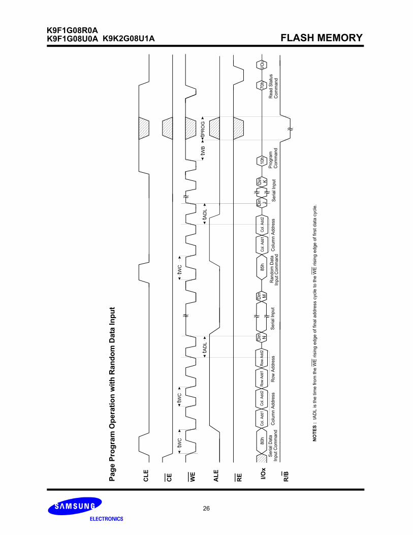
PAGE PROGRAMThe device is programmed basically on a page basis, but it does allow multiple partial page programing of a word or consecutivebytes up to 2112, in a single page program cycle. The number of consecutive partial page programming operation within the samepage without an intervening erase operation must not exceed 4 times for main array(1time/512byte) and 4 times for sparearray(1time/16byte). The addressing should be done in sequential order in a block. A page program cycle consists of a serial dataloading period in which up to 2112bytes of data may be loaded into the data register, followed by a non-volatile programming periodwhere the loaded data is programmed into the appropriate cell. The serial data loading period begins by inputting the Serial Data Input command(80h), followed by the four cycle address inputs andthen serial data loading. The words other than those to be programmed do not need to be loaded. The device supports random datainput in a page. The column address of next data, which will be entered, may be changed to the address which follows random datainput command(85h). Random data input may be operated multiple times regardless of how many times it is done in a page.The Page Program confirm command(10h) initiates the programming process. Writing 10h alone without previously entering theserial data will not initiate the programming process. The internal write state controller automatically executes the algorithms and tim-ings necessary for program and verify, thereby freeing the system controller for other tasks. Once the program process starts, theRead Status Register command may be entered to read the status register. The system controller can detect the completion of a pro-gram cycle by monitoring the R/B output, or the Status bit(I/O 6) of the Status Register. Only the Read Status command and Resetcommand are valid while programming is in progress. When the Page Program is complete, the Write Status Bit(I/O 0) may bechecked(Figure 8). The internal write verify detects only errors for "1"s that are not successfully programmed to "0"s. The commandregister remains in Read Status command mode until another valid command is written to the command register.
Figure 8. Program & Read Status Operation
80h
R/B
Address & Data Input I/O0 Pass
Data
10h 70h
Fail
tPROG
I/Ox
I/Ox
Col Add1,2 & Row Add1,2
"0"
"1"
Col Add1,2 & Row Add1,2
34
K9F1G08U0AK9F1G08R0A
K9K2G08U1A FLASH MEMORY
Cache Program
Figure 9. Random Data Input In a Page
80h
R/B
Address & Data Input I/O0 Pass10h 70h
Fail
tPROG
85h Address & Data Input
Cache Program is an extension of Page Program, which is executed with 2112byte data registers, and is available only within a block.Since the device has 1 page of cache memory, serial data input may be executed while data stored in data register are programmedinto memory cell.
After writing the first set of data up to 2112byte into the selected cache registers, Cache Program command (15h) instead of actualPage Program (10h) is inputted to make cache registers free and to start internal program operation. To transfer data from cache reg-isters to data registers, the device remains in Busy state for a short period of time(tCBSY) and has its cache registers ready for thenext data-input while the internal programming gets started with the data loaded into data registers. Read Status command (70h) maybe issued to find out when cache registers become ready by polling the Cache-Busy status bit(I/O 6). Pass/fail status of only the pre-viouse page is available upon the return to Ready state. When the next set of data is inputted with the Cache Program command,tCBSY is affected by the progress of pending internal programming. The programming of the cache registers is initiated only when thepending program cycle is finished and the data registers are available for the transfer of data from cache registers. The status bit(I/O5) for internal Ready/Busy may be polled to identify the completion of internal programming. If the system monitors the progress ofprogramming only with R/B, the last page of the target programming sequence must be progammed with actual Page Program com-mand (10h).
Figure 10. Cache Program(available only within a block)
80h
R/B
80h Address & Data Input 15h 80h Address &
Data Input 15h 80h Address & Data Input
10h
tCBSY tCBSY tCBSY tPROG
70h Address & Data Input* 15h
I/OxCol Add1,2 & Row Add1,2 Col Add1,2
Data Data
Col Add1,2 & Row Add1,2 Col Add1,2 & Row Add1,2 Col Add1,2 & Row Add1,2Data Data Data
Col Add1,2 & Row Add1,2Data
"0"
"1"
35
K9F1G08U0AK9F1G08R0A
K9K2G08U1A FLASH MEMORY
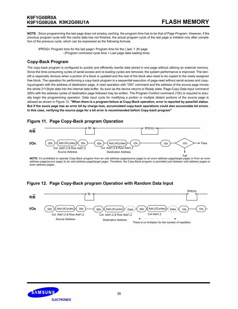
Copy-Back Program
Figure 11. Page Copy-Back program Operation
00h
R/B
Add.(4Cycles) I/O0 Pass85h 70h
Fail
tPROG
Add.(4Cycles)
tR
Source Address Destination Address
The copy-back program is configured to quickly and efficiently rewrite data stored in one page without utilizing an external memory.Since the time-consuming cycles of serial access and re-loading cycles are removed, the system performance is improved. The ben-efit is especially obvious when a portion of a block is updated and the rest of the block also need to be copied to the newly assignedfree block. The operation for performing a copy-back program is a sequential execution of page-read without serial access and copy-ing-program with the address of destination page. A read operation with "35h" command and the address of the source page movesthe whole 2112byte data into the internal data buffer. As soon as the device returns to Ready state, Page-Copy Data-input command(85h) with the address cycles of destination page followed may be written. The Program Confirm command (10h) is required to actu-ally begin the programming operation. Data input cycle for modifying a portion or multiple distant portions of the source page isallowed as shown in Figure 12. "When there is a program-failure at Copy-Back operation, error is reported by pass/fail status.But if the soure page has an error bit by charge loss, accumulated copy-back operations could also accumulate bit errors.In this case, verifying the source page for a bit error is recommended before Copy-back program"
35h
NOTE : Since programming the last page does not employ caching, the program time has to be that of Page Program. However, if theprevious program cycle with the cache data has not finished, the actual program cycle of the last page is initiated only after comple-tion of the previous cycle, which can be expressed as the following formula. tPROG= Program time for the last page+ Program time for the ( last -1 )th page - (Program command cycle time + Last page data loading time)
10h
Figure 12. Page Copy-Back program Operation with Random Data Input
00h
R/B
Add.(4Cycles) 85h 70h
tPROG
Add.(4Cycles)
tR
Source Address Destination Address
Data35h 10h85h DataAdd.(2Cycles)
There is no limitation for the number of repetition.
NOTE: It’s prohibited to operate Copy-Back program from an odd address page(source page) to an even address page(target page) or from an evenaddress page(source page) to an odd address page(target page). Therefore, the Copy-Back program is permitted just between odd address pages oreven address pages .
36
K9F1G08U0AK9F1G08R0A
K9K2G08U1A FLASH MEMORY
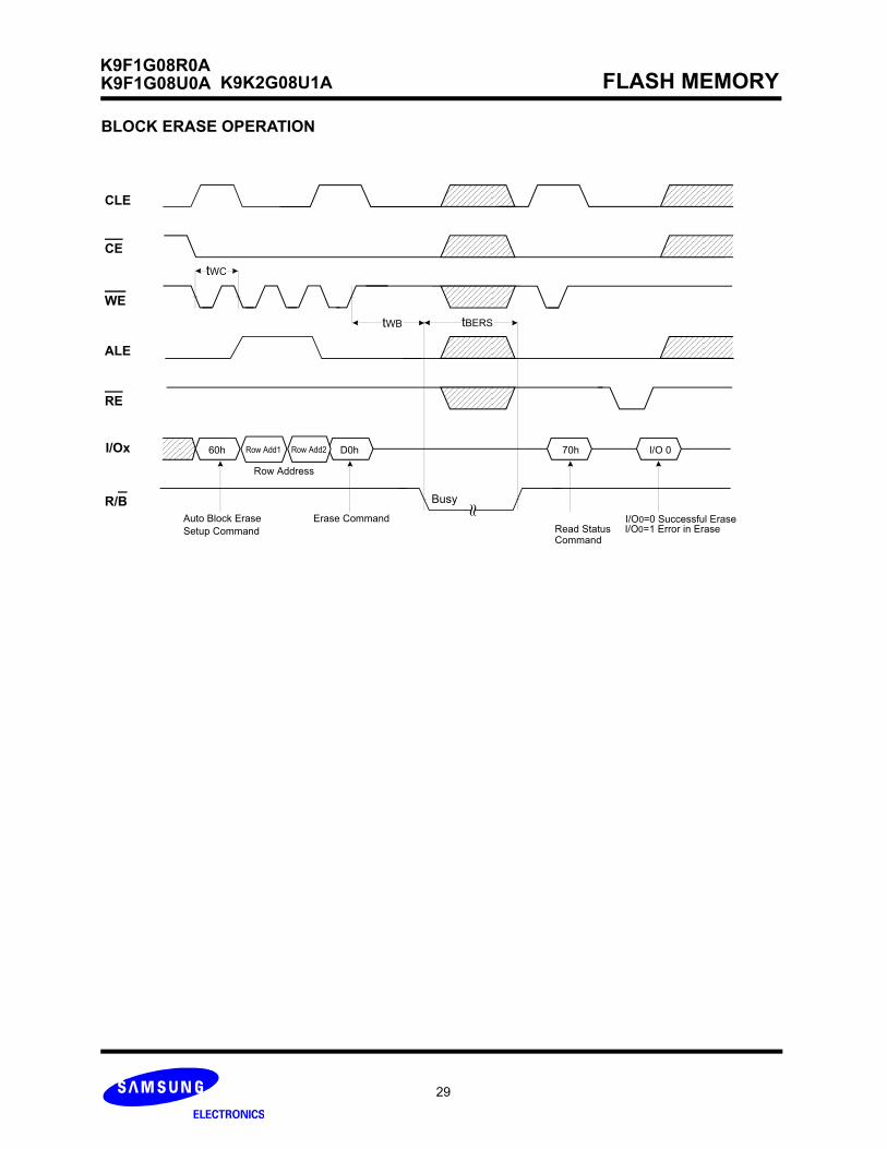
Figure 13. Block Erase Operation
BLOCK ERASEThe Erase operation is done on a block basis. Block address loading is accomplished in two cycles initiated by an Erase Setup com-mand(60h). Only address A18 to A27 is valid while A12 to A17 is ignored. The Erase Confirm command(D0h) following the blockaddress loading initiates the internal erasing process. This two-step sequence of setup followed by execution command ensures thatmemory contents are not accidentally erased due to external noise conditions.At the rising edge of WE after the erase confirm command input, the internal write controller handles erase and erase-verify. Whenthe erase operation is completed, the Write Status Bit(I/O 0) may be checked. Figure 13 details the sequence.
60h
Block Add. : A12 ~ A27
R/B
Address Input(2Cycle) I/O0 PassD0h 70h
Fail
tBERS
READ STATUSThe device contains a Status Register which may be read to find out whether program or erase operation is completed, and whetherthe program or erase operation is completed successfully. After writing 70h command to the command register, a read cycle outputsthe content of the Status Register to the I/O pins on the falling edge of CE or RE, whichever occurs last. This two line control allowsthe system to poll the progress of each device in multiple memory connections even when R/B pins are common-wired. RE or CEdoes not need to be toggled for updated status. Refer to table 2 for specific Status Register definitions. The command registerremains in Status Read mode until further commands are issued to it. Therefore, if the status register is read during a random readcycle, the read command(00h) should be given before starting read cycles.
Table2. Read Staus Register Definition
NOTE : 1. True Ready/Busy represents internal program operation status which is being executed in cache program mode. 2. I/Os defined ’Not use’ are recommended to be masked out when Read Status is being executed.
I/O No. Page Program Block Erase Cache Prorgam Read Definition
I/O 0 Pass/Fail Pass/Fail Pass/Fail(N) Not use Pass : "0" Fail : "1"
I/O 1 Not use Not use Pass/Fail(N-1) Not use Pass : "0" Fail : "1"
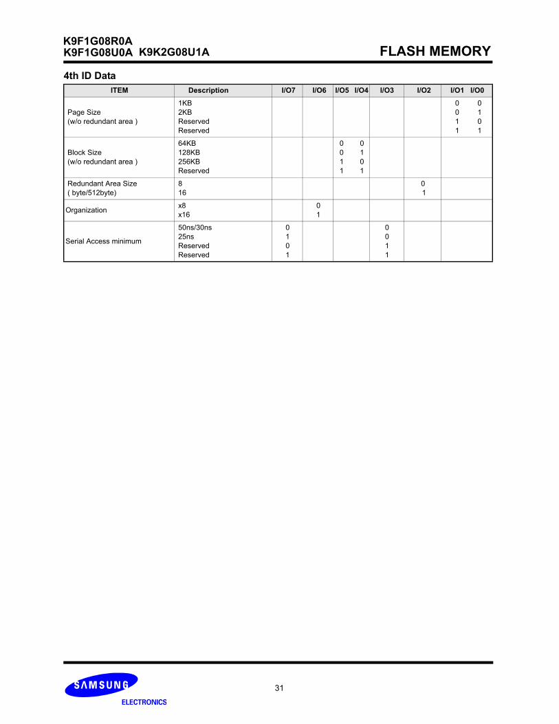
Read IDThe device contains a product identification mode, initiated by writing 90h to the command register, followed by an address input of00h. Four read cycles sequentially output the manufacturer code(ECh), and the device code and XXh, 4th cycle ID, respectively. Thecommand register remains in Read ID mode until further commands are issued to it. Figure 14 shows the operation sequence.
DeviceXXh 4th Cyc.*ECh
Figure 15. RESET Operation
RESETThe device offers a reset feature, executed by writing FFh to the command register. When the device is in Busy state during randomread, program or erase mode, the reset operation will abort these operations. The contents of memory cells being altered are nolonger valid, as the data will be partially programmed or erased. The command register is cleared to wait for the next command, andthe Status Register is cleared to value C0h when WP is high. Refer to table 3 for device status after reset operation.If the device isalready in reset state a new reset command will be accepted by the command register. The R/B pin transitions to low for tRST afterthe Reset command is written. Refer to Figure 15 below.
FFhI/OX
R/BtRST
tWHR
tCLR
Code*
Device Device Code*(2nd Cycle) 4th Cycle*
K9F1G08R0A A1h 15h
K9F1G08U0A F1h 15h
K9K2G08U1A Same as each K9F1G08U0A in it
Table3. Device StatusAfter Power-up After Reset
Operation Mode 00h command is latched Waiting for next command
38
K9F1G08U0AK9F1G08R0A
K9K2G08U1A FLASH MEMORY
READY/BUSYThe device has a R/B output that provides a hardware method of indicating the completion of a page program, erase and randomread completion. The R/B pin is normally high but transitions to low after program or erase command is written to the command regis-ter or random read is started after address loading. It returns to high when the internal controller has finished the operation. The pin isan open-drain driver thereby allowing two or more R/B outputs to be Or-tied. Because pull-up resistor value is related to tr(R/B) andcurrent drain during busy(ibusy) , an appropriate value can be obtained with the following reference chart(Fig 17). Its value can bedetermined by the following guidance.
where IL is the sum of the input currents of all devices tied to the R/B pin.
Rp value guidance
Rp(max) is determined by maximum permissible limit of tr
Rp(min, 3.3V part) =VCC(Max.) - VOL(Max.)
IOL + ΣIL =
3.2V
8mA + ΣIL
39
K9F1G08U0AK9F1G08R0A
K9K2G08U1A FLASH MEMORY
Data Protection & Power up sequenceThe device is designed to offer protection from any involuntary program/erase during power-transitions. An internal voltage detectordisables all functions whenever Vcc is below about 1.1V(1.8V device), 2V(3.3V device). WP pin provides hardware protection and isrecommended to be kept at VIL during power-up and power-down. A recovery time of minimum 10µs is required before internal circuitgets ready for any command sequences as shown in Figure 17. The two step command sequence for program/erase provides addi-tional software protection.
Figure 17. AC Waveforms for Power Transition
VCC
WP
High
WE
1.8V device : ~ 1.5V3.3V device : ~ 2.5V
1.8V device : ~ 1.5V3.3V device : ~ 2.5V
10µs
≈≈
≈≈
40
K9F1G08U0AK9F1G08R0A
K9K2G08U1A FLASH MEMORY
CL (F)
Figure 19. Rp vs tRHOH vs CL
Rp = 10k
@ Vcc = 3.3V, Ta = 25°C
30p 50p 70p 100p
50n
100n
36
6085
120
tRLOH / tRHOH value guidance
Figure 18. Serial Access Cycle after Read(EDO Type, CLE=L, WE=H, ALE=L)
300n
500n
180
300
425
600Rp = 100k
200n
400n
600n
360
600
VCC
Device
GND
Rp
CL
I/O Drive
tRHOH
Rp = 50k
3042 60
18
Rp = 5k
RE
CE
R/B
I/Ox
≈tRR
tCEA
tREA
tRP tREH
tRC
≈
tRHOHtRLOH
≈≈
Dout Dout
tREA
≈
NOTES : Transition is measured at ±200mV from steady state voltage with load. This parameter is sampled and not 100% tested.
tRHOH
tRHOH = CL * VOL * Rp / VcctRLOH(min, 3.3V part) = tRHOH - tREH
Extended Data Out ModeFor the EDO mode, the device should hold the data on the system memory bus until the beginning of the next cycle, so that controllercould fetch the data at the falling edge. However NAND flash dosen’t support the EDO mode exactly.The device stops the data input into the I/O bus after RE rising edge. But since the previous data remains in the I/O bus, the flow of I/O data seems like Figure 18 and the system can access serially the data with EDO mode. tRLOH which is the parameter for fetchingdata at RE falling time is necessary. Its appropriate value can be obtained with the reference chart as shown in Figure 19. The tRHOHvalue depands on output load(CL) and I/O bus Pull-up resistor (Rp).