Document version 0.3 1/34 Product Specification B121EW07 V1 AU OPTRONICS CORPORATION Product Specification 12.1” WXGA Color TFT-LCD Module Model Name: B121EW07 V1 Approved by Prepared by Kendra Wang Pei-Ching Huang NBBU Marketing Division / AU Optronics corporation Customer Checked & Approved by
Transcript
Document version 0.3 1/34
Product Specification
B121EW07 V1
AU OPTRONICS CORPORATION
Product Specification
12.1” WXGA Color TFT-LCD Module
Model Name: B121EW07 V1
Approved by Prepared by
Kendra Wang Pei-Ching Huang
NBBU Marketing Division / AU Optronics corporation
Customer Checked & Approved by
Document version 0.3 2/34
Product Specification
B121EW07 V1
Product Specification
12.1” WXGA Color TFT-LCD Module Model Name: B121EW07
V.1
( V ) Preliminary Specifications ( ) Final Specifications
Note: This Specification is subject to change without notice.
Optical Rise Time/Fall Time [msec] 25 typ. / 35 max.
Nominal Input Voltage VDD [Volt] +3.3 typ.
Typical Power Consumption [Watt] 4.5W max. (@85% LED driver efficiency)
Weight (with LED driver board) [Grams] 230g typ. 245g max
Physical Size [mm] 275.82x 179.4 x 5.1 max.
Electrical Interface 1 channel LVDS
Surface Treatment Glare
Document version 0.3 7/34
Product Specification
B121EW07 V1
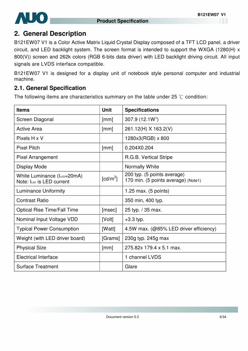
Support Color Native 262K colors ( RGB 6-bit data driver )
Temperature Range Operating Storage (Non-Operating)
[oC]
[oC]
0 to +50
-20 to +60
RoHS Compliance RoHS Compliance
2.2. Optical Characteristics
The optical characteristics are measured under stable conditions at 25℃ (Room Temperature):
Item Unit Conditions Min. Typ. Max. Note
White Luminance LED 20.0mA
[cd/m2]
5 points average
170 200 - 1,2,3
[degree] [degree]
Horizontal (Right) CR = 10 (Left)
-
-
40
40
-
- Viewing Angle
[degree] [degree]
Vertical (Upper) CR = 10 (Lower)
-
-
20
40
-
-
2,7
Uniformity 5 Points - - 1.25 1
CR: Contrast Ratio 350 400 - 6
Cross talk % - - 4 4
Response Time [msec] Raising + Falling - 25 35
Red x 0.530 0.580 0.630
Red y 0.280 0.330 0.380
Green x 0.275 0.325 0.375
Green y 0.515 0.565 0.615
Blue x 0.100 0.150 0.200
Blue y 0.070 0.120 0.170
White x 0.263 0.313 0.363
Color / Chromaticity Coordinates (CIE 1931)
White y 0.279 0.329 0.379
2,7
Document version 0.3 8/34
Product Specification
B121EW07 V1
Note 1: 5 points position (Display area: 261.12mm x 163.2mm)
1 2
3
4 5
H /4
H /4
H /4
H /4
H
W
W /4 W /4 W /4 W /4
Note 2: The luminance uniformity of 5 and 13 points is defined by dividing the maximum luminance values by the minimum test point luminance
δW13 =
Maximum Brightness of thirteen points Minimum Brightness of thirteen points
Maximum Brightness of five points δW5 = Minimum Brightness of five points
Document version 0.3 9/34
Product Specification
B121EW07 V1
Note 3: Measurement method
The LCD module should be stabilized at given temperature for 30 minutes to avoid abrupt temperature change during
measuring. In order to stabilize the luminance, the measurement should be executed after lighting Backlight for 30 minutes
in a stable, windless and dark room.
Note 4: Definition of Cross Talk (CT)
CT = | YB – YA | / YA × 100 (%)
Where
YA = Luminance of measured location without gray level 0 pattern (cd/m2)
YB = Luminance of measured location with gray level 0 pattern (cd/m2)
Center of the screen
TFT-LCD Module
50 cm
Photo detector
LCD Panel
Field=2°
Document version 0.3 10/34
Product Specification
B121EW07 V1
Note 5: Definition of response time:
The output signals of BM-7 or equivalent are measured when the input signals are changed from “Black” to “White”
(falling time) and from “White” to “Black” (rising time), respectively. The response time interval between the 10% and 90%
of amplitudes. Refer to figure as below.
Note 6: Definition of viewing angle
Viewing angle is the measurement of contrast ratio 10, at the screen center, over a 180° horizontal and 180° ≧vertical range (off-normal viewing angles). The 180° viewing angle range is broken down as follows; 90° (θ) horizontal
left and right and 90° (Φ) vertical, high (up) and low (down). The measurement direction is typically perpendicular to the
display surface with the screen rotated about its center to develop the desired measurement viewing angle.
Sig
nal (R
ela
tive v
alu
e)
"Black"
Tr Tf
"White""White"
0%10%
90%100%
Document version 0.3 11/34
Product Specification
B121EW07 V1
3. Functional Block Diagram The following diagram shows the functional block of the 12.1 inches wide Color TFT/LCD Module:
Document version 0.3 12/34
Product Specification
B121EW07 V1
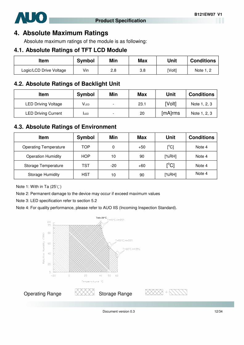
4. Absolute Maximum Ratings Absolute maximum ratings of the module is as following:
4.1. Absolute Ratings of TFT LCD Module
Item Symbol Min Max Unit Conditions
Logic/LCD Drive Voltage Vin 2.8 3.8 [Volt] Note 1, 2
4.2. Absolute Ratings of Backlight Unit
Item Symbol Min Max Unit Conditions
LED Driving Voltage VLED - 23.1 [Volt] Note 1, 2, 3
LED Driving Current ILED - 20 [mA]rms Note 1, 2, 3
4.3. Absolute Ratings of Environment
Item Symbol Min Max Unit Conditions
Operating Temperature TOP 0 +50 [oC] Note 4
Operation Humidity HOP 10 90 [%RH] Note 4
Storage Temperature TST -20 +60 [oC] Note 4
Storage Humidity HST 10 90 [%RH] Note 4
Note 1: With in Ta (25 )℃
Note 2: Permanent damage to the device may occur if exceed maximum values
Note 3: LED specification refer to section 5.2
Note 4: For quality performance, please refer to AUO IIS (Incoming Inspection Standard).
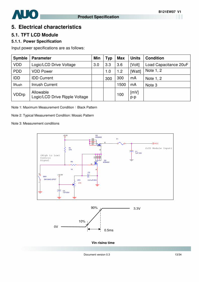
Input signals shall be low or Hi-Z state when VDD is off.
It is recommended to refer the specifications of THC63LVDF84A (Thine Electronics Inc.) in detail.
Signal electrical characteristics are as follows;
Parameter Condition Min Max Unit
Vth Differential Input High
Threshold (Vcm=+1.2V) 100 [mV]
Vtl Differential Input Low
Threshold (Vcm=+1.2V) -100 [mV]
Note: LVDS Signal Waveform
Vth
Vtl
Vcm
VSS
Document version 0.3 15/34
Product Specification
B121EW07 V1
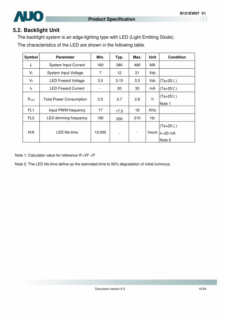
5.2. Backlight Unit
The backlight system is an edge-lighting type with LED (Light Emitting Diode).
The characteristics of the LED are shown in the following table.
Symbol Parameter Min. Typ. Max. Unit Condition
IL System Input Current 160 280 480 MA
VL System Input Voltage 7 12 21 Vdc
VF LED Foward Voltage 3.0 3.15 3.3 Vdc (Ta=25℃)
IF LED Foward Current - 20 30 mA (Ta=25℃)
PLED Total Power Consumption 2.5 2.7 2.8 W (Ta=25℃)
Note 1
FL1 Input PWM frequency 17 17.5 18 KHz
FL2 LED dimming frequency 190 200 210 Hz
N/A LED life-time 10,000 - - hours
(Ta=25℃)
IF=20 mA
Note 2
Note 1: Calculator value for reference IF×VF =P
Note 2: The LED life-time define as the estimated time to 50% degradation of initial luminous.
Document version 0.3 16/34
Product Specification
B121EW07 V1
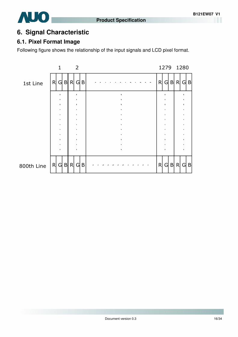
6. Signal Characteristic
6.1. Pixel Format Image
Following figure shows the relationship of the input signals and LCD pixel format.
R G B R G B
R G B R G B
R G B R G B
R G B R G B
1 2 1279 1280
1st Line
800th Line
Document version 0.3 17/34
Product Specification
B121EW07 V1
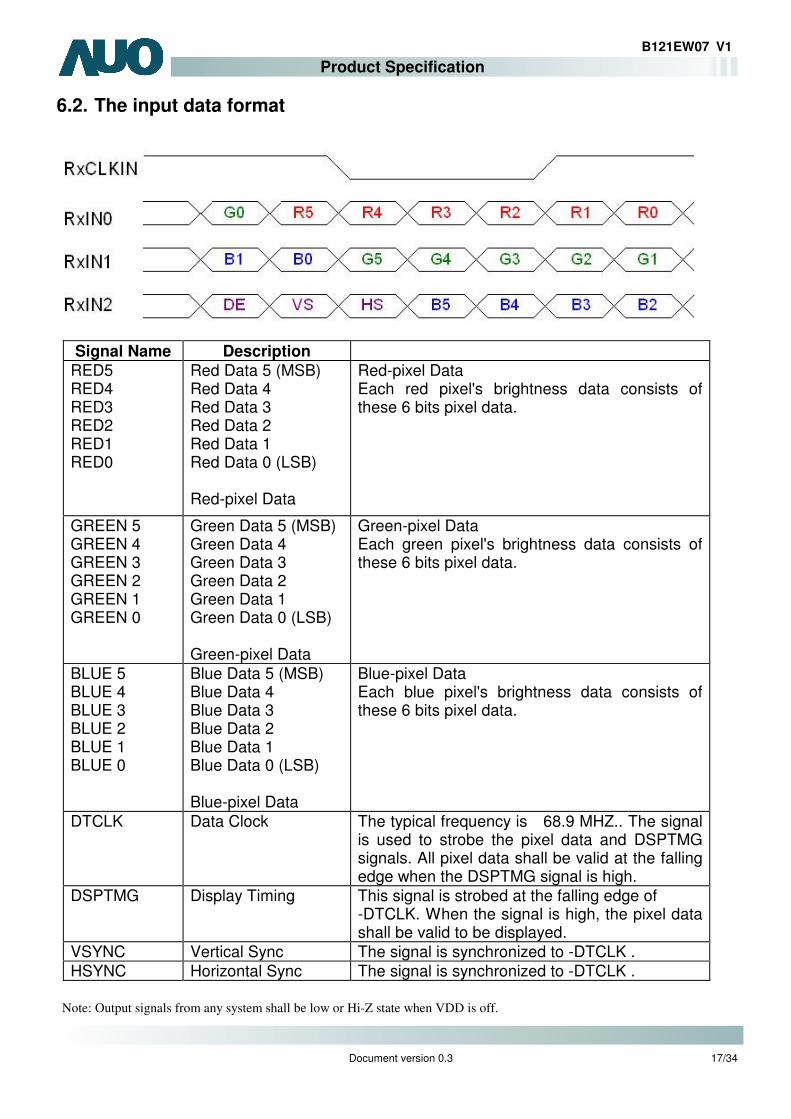
6.2. The input data format
Signal Name Description
RED5 RED4 RED3 RED2 RED1 RED0
Red Data 5 (MSB) Red Data 4 Red Data 3 Red Data 2 Red Data 1 Red Data 0 (LSB) Red-pixel Data
Red-pixel Data Each red pixel's brightness data consists of these 6 bits pixel data.
GREEN 5 GREEN 4 GREEN 3 GREEN 2 GREEN 1 GREEN 0
Green Data 5 (MSB) Green Data 4 Green Data 3 Green Data 2 Green Data 1 Green Data 0 (LSB) Green-pixel Data
Green-pixel Data Each green pixel's brightness data consists of these 6 bits pixel data.
BLUE 5 BLUE 4 BLUE 3 BLUE 2 BLUE 1 BLUE 0
Blue Data 5 (MSB) Blue Data 4 Blue Data 3 Blue Data 2 Blue Data 1 Blue Data 0 (LSB) Blue-pixel Data
Blue-pixel Data Each blue pixel's brightness data consists of these 6 bits pixel data.
DTCLK Data Clock The typical frequency is 68.9 MHZ.. The signal is used to strobe the pixel data and DSPTMG signals. All pixel data shall be valid at the falling edge when the DSPTMG signal is high.
DSPTMG Display Timing This signal is strobed at the falling edge of -DTCLK. When the signal is high, the pixel data shall be valid to be displayed.
VSYNC Vertical Sync The signal is synchronized to -DTCLK .
HSYNC Horizontal Sync The signal is synchronized to -DTCLK .
Note: Output signals from any system shall be low or Hi-Z state when VDD is off.
Document version 0.3 18/34
Product Specification
B121EW07 V1
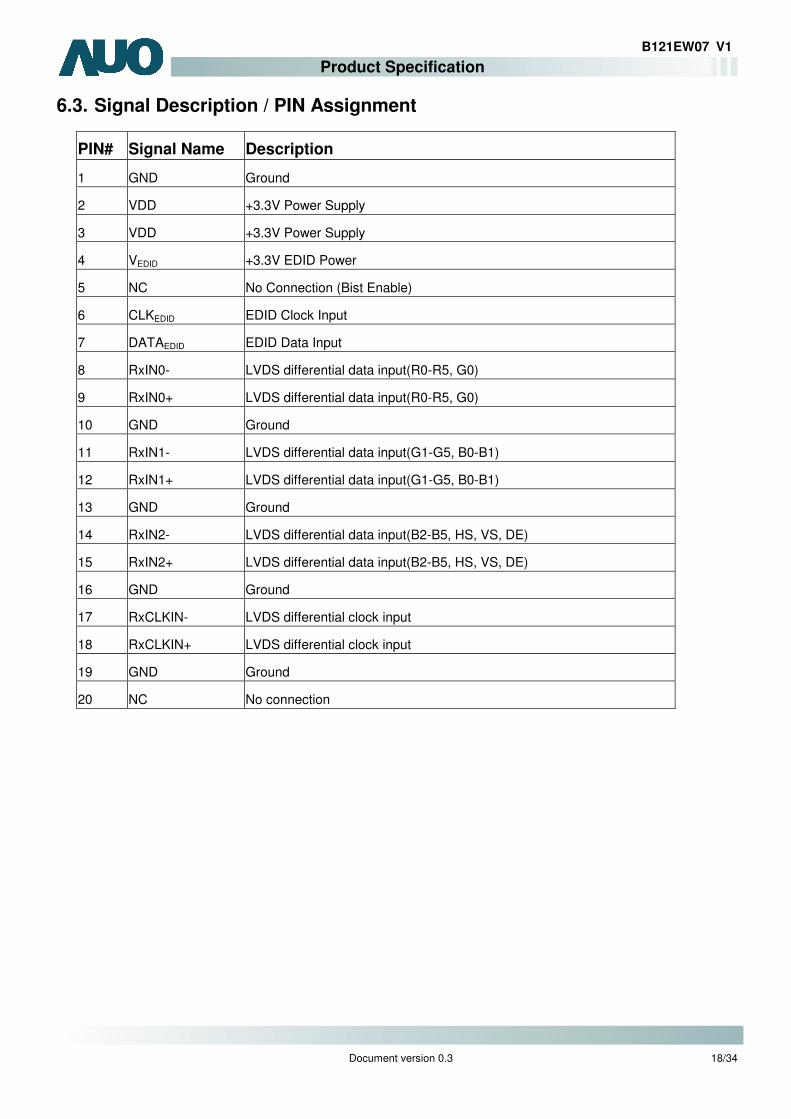
6.3. Signal Description / PIN Assignment
PIN# Signal Name Description
1 GND Ground
2 VDD +3.3V Power Supply
3 VDD +3.3V Power Supply
4 VEDID +3.3V EDID Power
5 NC No Connection (Bist Enable)
6 CLKEDID EDID Clock Input
7 DATAEDID EDID Data Input
8 RxIN0- LVDS differential data input(R0-R5, G0)
9 RxIN0+ LVDS differential data input(R0-R5, G0)
10 GND Ground
11 RxIN1- LVDS differential data input(G1-G5, B0-B1)
12 RxIN1+ LVDS differential data input(G1-G5, B0-B1)
13 GND Ground
14 RxIN2- LVDS differential data input(B2-B5, HS, VS, DE)
15 RxIN2+ LVDS differential data input(B2-B5, HS, VS, DE)
16 GND Ground
17 RxCLKIN- LVDS differential clock input
18 RxCLKIN+ LVDS differential clock input
19 GND Ground
20 NC No connection
Document version 0.3 19/34
Product Specification
B121EW07 V1
The module uses a 100ohm resistor between positive and negative data lines of each receiver input
R
R
R
R
Signal Input
Pin No.
9
11
12
14
15
17
18
8
RxIN0+
RxIN0-
RxIN1+
RxIN1-
RxIN2+
RxIN2-
RxCLKIN+
RxCLKIN-
LVDS Receiver
Document version 0.3 20/34
Product Specification
B121EW07 V1
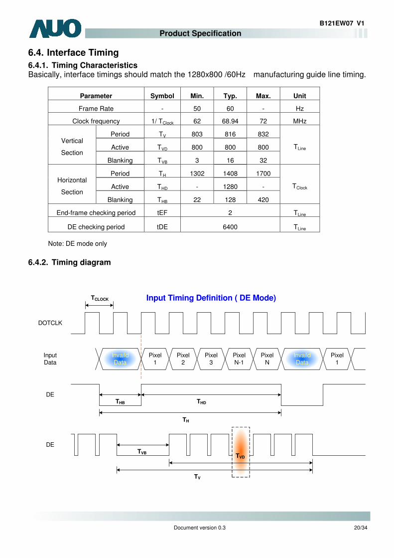
6.4. Interface Timing
6.4.1. Timing Characteristics Basically, interface timings should match the 1280x800 /60Hz manufacturing guide line timing.
Parameter Symbol Min. Typ. Max. Unit
Frame Rate - 50 60 - Hz
Clock frequency 1/ TClock 62 68.94 72 MHz
Period TV 803 816 832
Active TVD 800 800 800 Vertical
Section Blanking TVB 3 16 32
TLine
Period TH 1302 1408 1700
Active THD - 1280 - Horizontal
Section Blanking THB 22 128 420
TClock
End-frame checking period tEF 2 TLine
DE checking period tDE 6400 TLine
Note: DE mode only
6.4.2. Timing diagram
DOTCLK
DE
TH
THB THD
DE
TV
TVB TVD
Input Timing Definition ( DE Mode) TCLOCK
InputData
Pixel1
Pixel2
Pixel3
PixelN-1
PixelN
InvaildData
InvaildData
Pixel1
Document version 0.3 21/34
Product Specification
B121EW07 V1
6.5. Power ON/OFF Sequence VDD power and lamp on/off sequence is as follows. Interface signals are also shown in the chart. Signals from any system shall be Hi-Z state or low level when VDD is off.
Power Sequence Timing
Value Parameter
Min. Typ. Max. Units
T1 0.5 - 10 (ms)
T2 0 - 50 (ms)
T3 0 - 50 (ms)
T4 500 - - (ms)
T5 200 - - (ms)
T6 200 - - (ms)
T7 0 - 10 (ms)
T4 T3 T2
T5
VALID
DATA
T1
10%
90%
10%
90%
T6
T7 Power Supply VDD
LVDS Interface
Backlight On
Document version 0.3 22/34
Product Specification
B121EW07 V1
7. Connector Description
Physical interface is described as for the connector on module.
These connectors are capable of accommodating the following signals and will be following components.
7.1. TFT LCD Module
Connector Name / Designation For Signal Connector
Manufacturer Hirose
Type / Part Number DF19L-20P-1H
Mating Housing/Part Number DF19G-20S-1C or compatible
Document version 0.3 23/34
Product Specification
B121EW07 V1
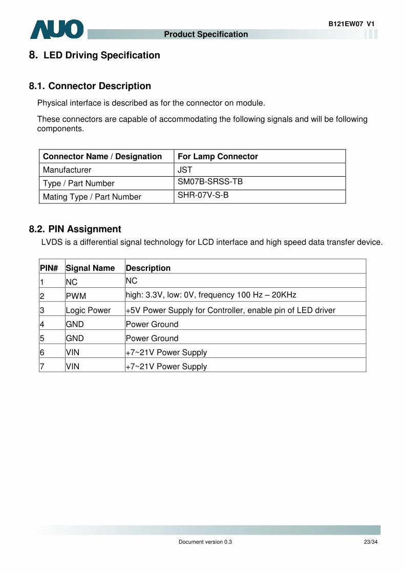
8. LED Driving Specification
8.1. Connector Description
Physical interface is described as for the connector on module.
These connectors are capable of accommodating the following signals and will be following components.
Connector Name / Designation For Lamp Connector
Manufacturer JST
Type / Part Number SM07B-SRSS-TB
Mating Type / Part Number SHR-07V-S-B
8.2. PIN Assignment
LVDS is a differential signal technology for LCD interface and high speed data transfer device.