KGD KGD Packaging and Test Workshop Packaging and Test Workshop, Napa, CA, September 8, 2003 PWB/Substrate Design Tutorial: Smith, Chang PWB/Substrate Design Tutorial Larry Smith, Ph.D. Chi-Shih Chang, Ph.D September 8, 2003
Transcript
KGDKGD Packaging and Test Workshop Packaging and Test Workshop, Napa, CA, September 8, 2003 PWB/Substrate Design Tutorial: Smith, Chang
PWB/Substrate Design Tutorial
Larry Smith, Ph.D.
Chi-Shih Chang, Ph.D
September 8, 2003
KGDKGD Packaging and Test Workshop Packaging and Test Workshop, Napa, CA, September 8, 2003 PWB/Substrate Design Tutorial: Smith, Chang
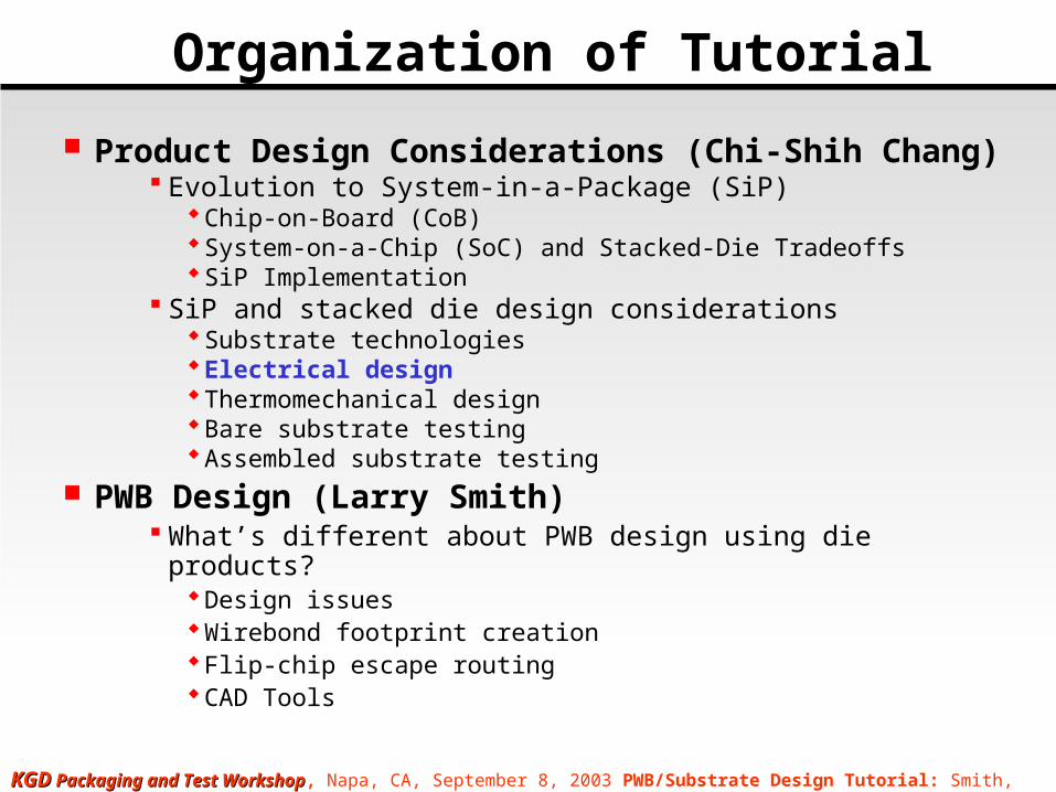
Organization of Tutorial
Product Design Considerations (Chi-Shih Chang) Evolution to System-in-a-Package (SiP)
Chip-on-Board (CoB)System-on-a-Chip (SoC) and Stacked-Die TradeoffsSiP Implementation
SiP and stacked die design considerationsSubstrate technologiesElectrical designThermomechanical designBare substrate testingAssembled substrate testing
PWB Design (Larry Smith) What’s different about PWB design using die products?
General design issuesWirebond designsFlip-chip designsCAD Tools
KGDKGD Packaging and Test Workshop Packaging and Test Workshop, Napa, CA, September 8, 2003 PWB/Substrate Design Tutorial: Smith, Chang
Introductions
Larry Smith Design Manager, K&S Substrate Division
BGA substrates for high IO flip-chip Program Manager, MicroModule Systems
KGDKGD Packaging and Test Workshop Packaging and Test Workshop, Napa, CA, September 8, 2003 PWB/Substrate Design Tutorial: Smith, Chang
Introductions (cont’d)
Chi-Shih Chang SMS Micro, Inc. provides consulting services for electronics
packaging and signal integrity VP of Adv. Products, High Connection Density, Inc. Strategic Applications Manager, K&S Senior Fellow, Sematech Member of the IBM Academy of Technology
Background Semiconductor devices, IC designs, and testing Electromagnetics and transmission lines Electrical design and signal integrity Packaging technologies ITRS AP-TWG member since 1995
KGDKGD Packaging and Test Workshop Packaging and Test Workshop, Napa, CA, September 8, 2003 PWB/Substrate Design Tutorial: Smith, Chang
Organization of Tutorial
Product Design Considerations (Chi-Shih Chang) Evolution to System-in-a-Package (SiP)
Chip-on-Board (CoB)System-on-a-Chip (SoC) and Stacked-Die TradeoffsSiP Implementation
SiP and stacked die design considerationsSubstrate technologiesElectrical designThermomechanical designBare substrate testingAssembled substrate testing
PWB Design (Larry Smith) What’s different about PWB design using die products?
KGDKGD Packaging and Test Workshop Packaging and Test Workshop, Napa, CA, September 8, 2003 PWB/Substrate Design Tutorial: Smith, Chang
Chip-on-Board (CoB): WB ICs
Bond fingers beyond die edges, allowing less dense PWB line width and spacing
Footprint on PWB much less than that of QFP Reduced connection length between ICs, less series
resistance, inductance & parasitic capacitance Use low modulus die adhesive to buffer the mismatch of the
coefficient of thermal expansion (CTE) of IC and that of PWB Programmable wire bonding accommodates future die shrink
without PWB redesign Wafer-level test & burn-in, if needed
KGDKGD Packaging and Test Workshop Packaging and Test Workshop, Napa, CA, September 8, 2003 PWB/Substrate Design Tutorial: Smith, Chang
WB IC Example
Source: M. Roston, et. al., “Assembly Challenges Related to Fine Pitch In-Line and Staggered Bond Pad Devices,” Proc. 53rd ECTC, May 28-30, 2003, New Orleans, pp. 1334-1343.
KGDKGD Packaging and Test Workshop Packaging and Test Workshop, Napa, CA, September 8, 2003 PWB/Substrate Design Tutorial: Smith, Chang
KGDKGD Packaging and Test Workshop Packaging and Test Workshop, Napa, CA, September 8, 2003 PWB/Substrate Design Tutorial: Smith, Chang
CoB: WLP ICs
Area array solder pads underneath die at 0.5-0.4 mm pitch, allowing relatively small number of I/Os
Footprint on PWB less than that of WB ICs Further reduced connection length between ICs Should reduce I/O array footprint (thus # I/Os) to a fraction of
the die size to facilitate future die shrink Wafer-level test & burn-in preferred. They may be made at
die-level, if necessary
KGDKGD Packaging and Test Workshop Packaging and Test Workshop, Napa, CA, September 8, 2003 PWB/Substrate Design Tutorial: Smith, Chang
CoB: Solder Flip-Chip ICs
Area array solder pads underneath die at 0.15-0.25 mm pitch, allowing a large number of I/Os
Large number of I/O pads available for V/G connections, capable of carrying current for high power IC. They also reduce inductance and switching noise
Large number of signal I/Os for wide data bus Very small footprint on PWB High density PWB needed Mismatch in CTE of IC and that of PWB presents a problem
for large IC, requiring underfill encapsulation
KGDKGD Packaging and Test Workshop Packaging and Test Workshop, Napa, CA, September 8, 2003 PWB/Substrate Design Tutorial: Smith, Chang
Solder Ball Flip Chip IC Example
KGDKGD Packaging and Test Workshop Packaging and Test Workshop, Napa, CA, September 8, 2003 PWB/Substrate Design Tutorial: Smith, Chang
CoB: Adhesive Flip-Chip ICs
Peripheral as well as area array connection pads underneath die at 0.1-0.2 mm pitch, allowing the maximum number of I/Os
Extremely high density PWB needed, unless number of I/O rows being limited
Minimum footprint on PWB Adhesive serves the function of underfill encapsulant to
mitigate CTE mismatch concern Relatively low temperature at assembly Limited current carrying capability, not suitable for high
current IC
KGDKGD Packaging and Test Workshop Packaging and Test Workshop, Napa, CA, September 8, 2003 PWB/Substrate Design Tutorial: Smith, Chang
Organization of Tutorial
Product Design Considerations (Chi-Shih Chang) Evolution to System-in-a-Package (SiP)
Chip-on-Board (CoB)System-on-a-Chip (SoC) and Stacked-Die TradeoffsSiP Implementation
SiP and stacked die design considerationsSubstrate technologiesElectrical designThermomechanical designBare substrate testingAssembled substrate testing
PWB Design (Larry Smith) What’s different about PWB design using die products?
Ease of useHigher level of reuse/lower costFaster time-to-market
ExamplesFlash on SRAM (smaller die on top)Flash on flash (same die size, a spacer needed)Memory on baseband ICProcessor on processor
Stacked-die enabling technologies Stacked-packages alternative
KGDKGD Packaging and Test Workshop Packaging and Test Workshop, Napa, CA, September 8, 2003 PWB/Substrate Design Tutorial: Smith, Chang
Stacked-Die Example -1
KGDKGD Packaging and Test Workshop Packaging and Test Workshop, Napa, CA, September 8, 2003 PWB/Substrate Design Tutorial: Smith, Chang
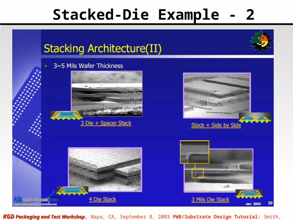
Stacked-Die Example - 2
KGDKGD Packaging and Test Workshop Packaging and Test Workshop, Napa, CA, September 8, 2003 PWB/Substrate Design Tutorial: Smith, Chang
Stacked-Die Enabling Technologies
Wafer thinning Die-to-die bonding Low loop height wire bonding Die attach control Thin and dense substrate High yield assembly process High quality die products Mechanical stress management Testing
KGDKGD Packaging and Test Workshop Packaging and Test Workshop, Napa, CA, September 8, 2003 PWB/Substrate Design Tutorial: Smith, Chang
Stacked-Packages Alternative
Larger footprint and larger height than stacked-die package Higher profile than stacked-die packages Flexibility in supply chain Test and burn-in at individual package level
KGDKGD Packaging and Test Workshop Packaging and Test Workshop, Napa, CA, September 8, 2003 PWB/Substrate Design Tutorial: Smith, Chang
Stacked-Package Comparison
Source: Y. Yano, et. al., “Three-dimensional Very Thin Stacked Packaging Technology for SiP,” Proc. 52nd ECTC, May 29-31, 2002, San Diego, pp. 1329-1334.
KGDKGD Packaging and Test Workshop Packaging and Test Workshop, Napa, CA, September 8, 2003 PWB/Substrate Design Tutorial: Smith, Chang
Organization of Tutorial
Product Design Considerations (Chi-Shih Chang) Evolution to System-in-a-Package (SiP)
Chip-on-Board (CoB)System-on-a-Chip (SoC) and Stacked-Die TradeoffsSiP Implementation
SiP and stacked die design considerationsSubstrate technologiesElectrical designThermomechanical designBare substrate testingAssembled substrate testing
PWB Design (Larry Smith) What’s different about PWB design using die products?
KGDKGD Packaging and Test Workshop Packaging and Test Workshop, Napa, CA, September 8, 2003 PWB/Substrate Design Tutorial: Smith, Chang
SiP Implementation
SiP applications and examplesPortable products – Cell phone, digital camera, …Baseband processor, application processor, flash
Include passives on SiP, instead of on the motherboard (improved signal integrity)
SiP benefits
KGDKGD Packaging and Test Workshop Packaging and Test Workshop, Napa, CA, September 8, 2003 PWB/Substrate Design Tutorial: Smith, Chang
SiP with WB & Passive
KGDKGD Packaging and Test Workshop Packaging and Test Workshop, Napa, CA, September 8, 2003 PWB/Substrate Design Tutorial: Smith, Chang
SiP with WB & CSP & Passive
KGDKGD Packaging and Test Workshop Packaging and Test Workshop, Napa, CA, September 8, 2003 PWB/Substrate Design Tutorial: Smith, Chang
SiP with FC & CSP & Passive
KGDKGD Packaging and Test Workshop Packaging and Test Workshop, Napa, CA, September 8, 2003 PWB/Substrate Design Tutorial: Smith, Chang
Embedded Passives in Substrate
Source: A. Okubora, et. al., “A Novel Integrated Passive Substrate Fabricated Directly on An Organic Laminate for RF Applications,” Proc. 52nd ECTC, May 29-31, 2002, San Diego, pp. 672-675.
KGDKGD Packaging and Test Workshop Packaging and Test Workshop, Napa, CA, September 8, 2003 PWB/Substrate Design Tutorial: Smith, Chang
SiP Benefits
Small form factor (lower PWB cost) Light weight for portable products Less aggressive I/O pitch than that with COB (lower PWB
KGDKGD Packaging and Test Workshop Packaging and Test Workshop, Napa, CA, September 8, 2003 PWB/Substrate Design Tutorial: Smith, Chang
Electrical Design
Power/ground distributionMultiple voltages on one plane
Signal lines (To be considered a transmission line?)Controlled impedance
Function (Line width, dielectric thickness, dielectric constant)
Signal crosstalkFunction (edge-to-edge spacing, dielectric thickness)NoiseMagnitude of received signal depending on data pattern (noise
immunity)Propagation time depending on data patterns (timing skew)
Migrate to “differential pair”
KGDKGD Packaging and Test Workshop Packaging and Test Workshop, Napa, CA, September 8, 2003 PWB/Substrate Design Tutorial: Smith, Chang
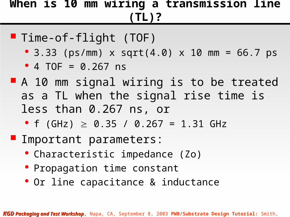
When is 10 mm wiring a transmission line (TL)?
Time-of-flight (TOF) 3.33 (ps/mm) x sqrt(4.0) x 10 mm = 66.7 ps 4 TOF = 0.267 ns
A 10 mm signal wiring is to be treated as a TL when the signal rise time is less than 0.267 ns, or f (GHz) 0.35 / 0.267 = 1.31 GHz
Important parameters: Characteristic impedance (Zo) Propagation time constant Or line capacitance & inductance
KGDKGD Packaging and Test Workshop Packaging and Test Workshop, Napa, CA, September 8, 2003 PWB/Substrate Design Tutorial: Smith, Chang
Effect of a transmission line (TL)
To get a 1.0 volt signal across a 50-ohm TL, 20 mA of current is required.
When the signal line width in the PWB reduces, it may become a 60-ohm TL. At this discontinuity, the voltage becomes 1.091 volts, and the current becomes 18.2 mA.
Excessive changes in voltage and current along a signal line may increase circuit delay time, reduces noise margin, or even impact circuit functionality.
This is a burden to circuit and system designers
KGDKGD Packaging and Test Workshop Packaging and Test Workshop, Napa, CA, September 8, 2003 PWB/Substrate Design Tutorial: Smith, Chang
Zo of a Transmission Line
Zo = (377/R)/[(WEFF/H1)+(WEFF/H2)+2.62(WEFF/H1)1/4]
WEFF (W + T) / 1.5, when 0.3 T / W 0.6Source: C.S. Chang, “Electrical Design Methodologies,” in Electronic Materials Handbook,
Volume 1 Packaging, ASM International, 1989, pp. 25-44.
KGDKGD Packaging and Test Workshop Packaging and Test Workshop, Napa, CA, September 8, 2003 PWB/Substrate Design Tutorial: Smith, Chang
Zo Dependence on Design Parameters
Zo is inversely proportional to sqrt (R)
Zo increases when H1 increases Zo decreases when W and/or T increases Zo has weak dependence on H2, where H2 > H1 In typical PWB, any change in W would change Zo. This
discontinuity in Zo would cause signal reflection (noise)
H2
T
H1
W
KGDKGD Packaging and Test Workshop Packaging and Test Workshop, Napa, CA, September 8, 2003 PWB/Substrate Design Tutorial: Smith, Chang
Design Consideration for Parallel TLs To reduce cross-talk noise, a second reference
plane is very beneficial. Reduce signal line width to maintain the same Zo. Low cross-talk noise also reduces the effect of data
patterns (in data bus and address bus) on: Noise margin of receiver circuits Effective signal propagation time
H2
T
H1
W S W
positive negative
KGDKGD Packaging and Test Workshop Packaging and Test Workshop, Napa, CA, September 8, 2003 PWB/Substrate Design Tutorial: Smith, Chang
Two Parallel Transmission Lines
One line active Adjacent line picks up noise
Both lines active Common mode: both switching
the same polarity Difference mode: switching on
opposite polarities
The propagation constant of common and difference modes are: C = C + jC = [(Z11 + Z12)(Y11 + Y12)]
0.5 (1) D = D + jD = [(Z11 - Z12)(Y11 - Y12)]
0.5 (2) For a lossless coupled lines, we have C = D = 0, and
C = [(L11 + L12)(C11 + C12)]0.5 (3)
D = [(L11 - L12)(C11 - C12)]0.5 (4)
Source: S. Kim, C. S. Chang, and D. P. Neikirk, “Impact of Cross-over lines on Delay Time of Two Parallel Global Wires,” IEEE 8th Topical Meeting on Electrical Performance of Electronic Packaging, 10/25-10/27/1999, San Diego, CA, pp. 53-56.
KGDKGD Packaging and Test Workshop Packaging and Test Workshop, Napa, CA, September 8, 2003 PWB/Substrate Design Tutorial: Smith, Chang
Low Voltage Differential Pair
Point-to-point wiring net with far-end terminationEliminate reflected signal (multiple bits sent before the
first bit arrive at far-end) Two signal lines for each signal port
Eliminate common mode noise (Simultaneous switching noise)
Drastically reduce signal cross-talk between adjacent pairs(Minimize delay time dependence on data patterns in the bus)
Receiver circuit needs very small voltage swingReduce power consumptionTolerate signal attenuation, less concern with skin-
effect and dielectric losses (Accommodate longer line or higher frequency)
KGDKGD Packaging and Test Workshop Packaging and Test Workshop, Napa, CA, September 8, 2003 PWB/Substrate Design Tutorial: Smith, Chang
Differential Pair Transmission Lines
Two signal lines for each signal (2X wiring requirements, but reduce voltage/ground I/O#)
Immune to noise on reference planes (Tolerate a reference plane split into multiple voltages)
Low cross-talk noise from adjacent signal pairs. Spacing within a signal pair needs tight control.
H2
T
H1
W S W
positive negative
KGDKGD Packaging and Test Workshop Packaging and Test Workshop, Napa, CA, September 8, 2003 PWB/Substrate Design Tutorial: Smith, Chang
Differential Pair Transmission Lines
Low voltage swing & low power consumption Differential receiver circuit can correctly sense an input signal
even when it is attenuated to 10% or less (Single-ended receiver circuit allows attenuation at about 70%.)
Tolerate higher attenuation Longer distance between input & output Higher frequency
Skin effect loss proportional to square root of frequency (smooth copper surface beneficial)
Dielectric loss proportional to frequency (low loss material desirable)
Often used for broadband data communications
KGDKGD Packaging and Test Workshop Packaging and Test Workshop, Napa, CA, September 8, 2003 PWB/Substrate Design Tutorial: Smith, Chang
Orthogonal Fan-out Wiring in PBGA
KGDKGD Packaging and Test Workshop Packaging and Test Workshop, Napa, CA, September 8, 2003 PWB/Substrate Design Tutorial: Smith, Chang
Organization of Tutorial
Product Design Considerations (Chi-Shih Chang) Evolution to System-in-a-Package (SiP)
Chip-on-Board (CoB)System-on-a-Chip (SoC) and Stacked-Die TradeoffsSiP Implementation
SiP and stacked die design considerationsSubstrate technologiesElectrical designThermomechanical designBare substrate testingAssembled substrate testing
PWB Design (Larry Smith) What’s different about PWB design using die products?
KGDKGD Packaging and Test Workshop Packaging and Test Workshop, Napa, CA, September 8, 2003 PWB/Substrate Design Tutorial: Smith, Chang
Thermomechanical Design
Total power of all dice in a stack converted to power per unit area
Low CTE(eff) of the stacked-die causes thermomechanical stress on substrate
Not a problem for a small dieUse low modulus die adhesive, spacer and
encapsulantUse low CTE substrate
KGDKGD Packaging and Test Workshop Packaging and Test Workshop, Napa, CA, September 8, 2003 PWB/Substrate Design Tutorial: Smith, Chang
Thermomechanical Stress
Source: Y. Li, “Accurate Predictions of Flip Chip BGA Warpage,” Proc. 53rd ECTC, May 28-30, 2003, New Orleans, pp. 549-553.
KGDKGD Packaging and Test Workshop Packaging and Test Workshop, Napa, CA, September 8, 2003 PWB/Substrate Design Tutorial: Smith, Chang
Failure Associated with Stress - 1
KGDKGD Packaging and Test Workshop Packaging and Test Workshop, Napa, CA, September 8, 2003 PWB/Substrate Design Tutorial: Smith, Chang
Failure Associated with Stress - 2
Source: Y. Naka, et. al., “Highly Reliable and Low-Cost Multi-Chip Module Composed of Wafer Process Packages,” Proc. 53rd ECTC, May 28-30, 2003, New Orleans, pp. 881-885.
KGDKGD Packaging and Test Workshop Packaging and Test Workshop, Napa, CA, September 8, 2003 PWB/Substrate Design Tutorial: Smith, Chang
Failure after Temperature Cycling
Source: T. Sugiyama, et. al., “Board Level Reliability of Three-Dimensional System in Package (SIPs),” Proc. 53rd ECTC, May 28-30, 2003, New Orleans, pp. 1106-1111.
KGDKGD Packaging and Test Workshop Packaging and Test Workshop, Napa, CA, September 8, 2003 PWB/Substrate Design Tutorial: Smith, Chang
Organization of Tutorial
Product Design Considerations (Chi-Shih Chang) Evolution to System-in-a-Package (SiP)
Chip-on-Board (CoB)System-on-a-Chip (SoC) and Stacked-Die TradeoffsSiP Implementation
SiP and stacked die design considerationsSubstrate technologiesElectrical designThermomechanical designBare substrate testingAssembled substrate testing
PWB Design (Larry Smith) What’s different about PWB design using die products?
KGDKGD Packaging and Test Workshop Packaging and Test Workshop, Napa, CA, September 8, 2003 PWB/Substrate Design Tutorial: Smith, Chang
Bare Substrate Testing
Identify in-process failure mechanisms for process development
Locate failure sites for in-process repairs Assure good products for customer shipping Final test may be made in whole panel or as an
individual substrateTest equipment capital costTime to feed an individual substrate or time to load the
panel and to step-and-repeat between substratesTest time per substrate x # substrates / panelChallenges: Fine pitch WB fingers & FC pads
KGDKGD Packaging and Test Workshop Packaging and Test Workshop, Napa, CA, September 8, 2003 PWB/Substrate Design Tutorial: Smith, Chang
Testing Methods
Automatic optical inspection (AOI) Bed-of-nails electrical tests for short (between
adjacent lines) & open (continuity failure)
Fine-pitch probe head for high-density WB fingers & FC pads (die I/Os)
ChallengesOpen between die I/O and substrate I/OShort & open between die sites on SiP
KGDKGD Packaging and Test Workshop Packaging and Test Workshop, Napa, CA, September 8, 2003 PWB/Substrate Design Tutorial: Smith, Chang
Assembled Substrate Testing
Assure all WB fingers or FC pads on substrate are connected to IC I/O pads at assembly
Functional testTo locate failure sites/components for repair, requiring
design-for-testTo assure good assembled substrates for customer
shipping
Build-in self test (BIST) strongly recommendedCo-design efforts from IC design to final product
KGDKGD Packaging and Test Workshop Packaging and Test Workshop, Napa, CA, September 8, 2003 PWB/Substrate Design Tutorial: Smith, Chang
Organization of Tutorial
Product Design Considerations (Chi-Shih Chang) Evolution to System-in-a-Package (SiP)
Chip-on-Board (CoB)System-on-a-Chip (SoC) and Stacked-Die TradeoffsSiP Implementation
SiP and stacked die design considerationsSubstrate technologiesElectrical designThermomechanical designBare substrate testingAssembled substrate testing
PWB Design (Larry Smith) What’s different about PWB design using die products?
General design issuesWirebond designsFlip-chip designsCAD Tools
KGDKGD Packaging and Test Workshop Packaging and Test Workshop, Napa, CA, September 8, 2003 PWB/Substrate Design Tutorial: Smith, Chang
PWB Design: Objectives / Approach
What’s different about PWB design using die products Summary of design issues Wirebond footprint creation Flip-chip escape routing CAD Tools
Focus on general issues and techniques rather than specific solutions:
Very broad spectrum of die, substrate technologies, product requirements, organizational environments
Not providing specific substrate and assembly design rules:Wide spectrum of design rules ranging from conventional to advancedMoving target, steadily shrinkingCompany confidential
KGDKGD Packaging and Test Workshop Packaging and Test Workshop, Napa, CA, September 8, 2003 PWB/Substrate Design Tutorial: Smith, Chang
PWB Design: Outline Overview: What’s different about PWB design for die products
Interface with Product Design Design for Assembly Routing CAD tools
Wirebond designs Design rules Footprint design SiP examples Relationship between wire length and finger pitch CAD Tools
KGDKGD Packaging and Test Workshop Packaging and Test Workshop, Napa, CA, September 8, 2003 PWB/Substrate Design Tutorial: Smith, Chang
(Selected) Wirebond Design Rules Bond finger dimensions, layer-to-layer rules
Bond finger length and width Minimum spacing bond finger shape
Chamfered or rounded corners Soldermask clearances Pad-trace minimum distance
Bond finger location Fanout pattern Minimum distance from die (die attach) Maximum wire length (wire sweep, wire droop) Spacing between rows (wire droop)
Wire rules Maximum angle (wire pitch at die corners) Wire-to-wire spacings (three-dimensions) Length-matching
KGDKGD Packaging and Test Workshop Packaging and Test Workshop, Napa, CA, September 8, 2003 PWB/Substrate Design Tutorial: Smith, Chang
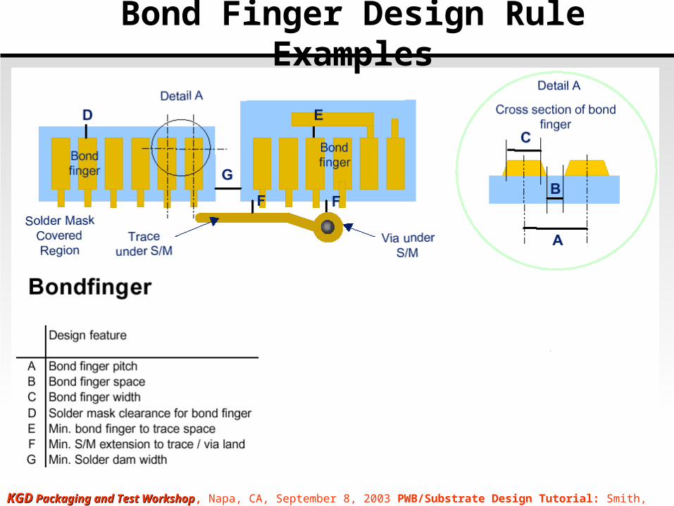
Bond Finger Design Rule Examples
KGDKGD Packaging and Test Workshop Packaging and Test Workshop, Napa, CA, September 8, 2003 PWB/Substrate Design Tutorial: Smith, Chang
Wirebond Fanout Pattern Examples
Ref:CAD Design Software:Hybrid/MCM Designer Suite
KGDKGD Packaging and Test Workshop Packaging and Test Workshop, Napa, CA, September 8, 2003 PWB/Substrate Design Tutorial: Smith, Chang
Wirebond Pad Footprint Design
Hard to have a “standard” footprint for a die Biggest difference in PWB design for bare die vs packaged die Depends on substrate and assembly design rules
Common to modify footprint for bonding variations: Design to support more than one version of die
Multiple suppliers Planned die revisions, shrinks May require use dummy pads
Bonding options Core logic and/or bus speed Supply voltage Test/debug Circuit changes
Need to edit footprint during placement/routing for system-in-a-package May modify pad locations to support denser placement CAD tool needs to support bond finger pad editing after creation
See examples below
KGDKGD Packaging and Test Workshop Packaging and Test Workshop, Napa, CA, September 8, 2003 PWB/Substrate Design Tutorial: Smith, Chang
PWB Design: Outline Overview: What’s different about PWB design for die products
Interface with Product Design Design for Assembly Routing CAD tools
Wirebond designs Design rules Footprint design SiP examples Relationship between wire length and finger pitch CAD Tools
KGDKGD Packaging and Test Workshop Packaging and Test Workshop, Napa, CA, September 8, 2003 PWB/Substrate Design Tutorial: Smith, Chang
CAD Tool Features Footprint creation
Patterns, orientations, shapes, power/ground rings Ability to edit bond fingers Support for multiple die sourcing
Stacked Die Basic support Constrain allowable wire-crossings Check wire clearances in three dimensions
Tolerance analysis 3D DRC
Pad sharing Manufacturing files
Ability to read industry standard files (*.LIQ and *.DIE) Wirebond diagrams Code to drive equipment
Bonders, … Support build-up technology
Stair-stepped vias
KGDKGD Packaging and Test Workshop Packaging and Test Workshop, Napa, CA, September 8, 2003 PWB/Substrate Design Tutorial: Smith, Chang
Wirebond Pad Creation in APD
Courtesy, Cadence Design Systems
KGDKGD Packaging and Test Workshop Packaging and Test Workshop, Napa, CA, September 8, 2003 PWB/Substrate Design Tutorial: Smith, Chang
Wirebond Pad Creation in Excel
KGDKGD Packaging and Test Workshop Packaging and Test Workshop, Napa, CA, September 8, 2003 PWB/Substrate Design Tutorial: Smith, Chang
Stacked Die
CAD tool supportSupport die data in multiple levelsMore complex footprint creationShared bondpadsDie-to-die connectionsCalculate clearances of bond wires based on bond
wire profiles and die placement tolerances. Examples
Cadence APDCAD Design Software
KGDKGD Packaging and Test Workshop Packaging and Test Workshop, Napa, CA, September 8, 2003 PWB/Substrate Design Tutorial: Smith, Chang
Stacked Die Examples
Advanced Packaging August, 2003Author(s) : Joel McGrath
Photo courtesy of ChipPAC Inc.
KGDKGD Packaging and Test Workshop Packaging and Test Workshop, Napa, CA, September 8, 2003 PWB/Substrate Design Tutorial: Smith, Chang
Cadence APD SiP Example
KGDKGD Packaging and Test Workshop Packaging and Test Workshop, Napa, CA, September 8, 2003 PWB/Substrate Design Tutorial: Smith, Chang
Stacked Die - CDS
Ref:CAD Design SoftwareStacked Die Manufacturing Designer Suite
KGDKGD Packaging and Test Workshop Packaging and Test Workshop, Napa, CA, September 8, 2003 PWB/Substrate Design Tutorial: Smith, Chang
PWB Design: Outline Overview: What’s different about PWB design for die products
Interface with Product Design Design for Assembly Routing CAD tools
Wirebond designs Design rules Footprint design SiP examples Relationship between wire length and finger pitch CAD Tools
Line Width (µm) 11.4 11.4 10.7 10.7 9.2 9.2 8.5 6.4 5.7 5 Line Spacing (µm) 11.4 11.4 10.7 10.7 9.3 9.3 8.6 6.4 5.7 5* The pad size is assumed as 50% of pad pitch. It is usually different at different fan-out layers, e.g. from 30% to 60%
Line Width (µm) 107 48 43 39 Line Spacing (µm) 107 48 43 39
Line Width (µm) 68 31 27 25 Line Spacing (µm) 68 31 27 25
Line Width (µm) 36 16 14 13 Line Spacing (µm) 36 16 14 13* The pad size is assumed as 50% of pad pitch. It is usually different at different fan-out layers, e.g. from 30% to 60%


![PWB Handbook[1]](https://static.documents.pub/doc/80x56/577d25b71a28ab4e1e9f734a/pwb-handbook1.jpg)


