103
Kinetis V Series Peripheral Module Quick Reference Document Number: KVQRUG Rev 0, 02/2014

Kinetis V Series Peripheral ModuleQuick Reference
Document Number: KVQRUGRev 0, 02/2014

Kinetis V Series Peripheral Module Quick Reference, Rev. 0, 02/2014
2 Freescale Semiconductor, Inc.

Contents
Section number Title Page
Chapter 1General System Setup (Software Considerations)
1.1 Software considerations..................................................................................................................................................9
1.1.1 Overview............................................................................................................................................................9
1.1.2 Code execution...................................................................................................................................................9
1.1.3 Reset and booting...............................................................................................................................................9
1.1.3.1 Device state during reset....................................................................................................................10
1.1.3.2 Device state after reset.......................................................................................................................10
1.1.4 Typical system initialization .............................................................................................................................10
1.1.4.1 Lowest level assembly routines.........................................................................................................10
1.1.4.1.1 Initialize general purpose registers...................................................................................10
1.1.4.1.1.1 Unmask interrupts at ARM® core ...............................................................11
1.1.4.1.1.2 Branch to start of C initialization code.........................................................11
1.1.4.2 Startup routines..................................................................................................................................11
1.1.4.2.1 Disable watchdog..............................................................................................................11
1.1.4.2.2 Initialize RAM..................................................................................................................11
1.1.4.2.3 Enable port clocks.............................................................................................................11
1.1.4.2.4 Ramp system clock to selected frequency........................................................................12
1.1.4.2.5 Enable UART for terminal communication......................................................................12
1.1.4.2.6 Jump to start of main function for application..................................................................12
Chapter 2General System Setup (Hardware Considerations)
2.1 Hardware considerations.................................................................................................................................................13
2.1.1 Overview............................................................................................................................................................13
2.1.2 Floorplan............................................................................................................................................................13
2.1.2.1 Connectors.........................................................................................................................................14
2.1.3 PCB routing considerations...............................................................................................................................14
2.1.3.1 Power supply routing.........................................................................................................................14
Kinetis V Series Peripheral Module Quick Reference, Rev. 0, 02/2014
Freescale Semiconductor, Inc. 3
Section number Title Page
2.1.3.2 Power supply decoupling and filtering..............................................................................................15
2.1.3.3 Oscillators..........................................................................................................................................15
2.1.3.3.1 MCG oscillator..................................................................................................................15
2.1.3.4 General filtering.................................................................................................................................18
2.1.3.4.1 RESET_b and NMI_b.......................................................................................................18
2.1.3.4.2 General purpose I/O..........................................................................................................19
2.1.3.4.3 Analog inputs....................................................................................................................19
2.1.4 PCB layer stack-up.............................................................................................................................................19
2.1.5 Other module hardware considerations..............................................................................................................22
2.1.5.1 Debug interface..................................................................................................................................22
Chapter 3Nested Vector Interrupt Controller (NVIC)
3.1 NVIC...............................................................................................................................................................................25
3.1.1 Overview............................................................................................................................................................25
3.1.1.1 Introduction .......................................................................................................................................25
3.1.1.2 Features .............................................................................................................................................25
3.1.2 Configuration examples.....................................................................................................................................26
3.1.2.1 Configuring the NVIC.......................................................................................................................26
3.1.2.1.1 Code example and explanation.........................................................................................26
3.1.2.2 Relocating the vector table.................................................................................................................27
3.1.2.2.1 Code example and explanation.........................................................................................28
Chapter 4Clocking System
4.1 Clocking..........................................................................................................................................................................29
4.1.1 Overview............................................................................................................................................................29
4.1.2 Features..............................................................................................................................................................29
4.1.3 Configuration examples.....................................................................................................................................31
4.1.4 Clocking system device hardware implementation...........................................................................................33
4.1.5 Layout guidelines for general routing and placement........................................................................................34
Kinetis V Series Peripheral Module Quick Reference, Rev. 0, 02/2014
4 Freescale Semiconductor, Inc.
Section number Title Page
4.1.6 References..........................................................................................................................................................34
Chapter 5Power Management Control (PMC/SMC/LLWU/RCM)
5.1 Introduction.....................................................................................................................................................................37
5.2 Using the power management controller........................................................................................................................37
5.2.1 Overview............................................................................................................................................................37
5.2.2 Using the low voltage detection system.............................................................................................................37
5.2.2.1 POR and LVD features......................................................................................................................37
5.2.2.2 Configuration examples.....................................................................................................................38
5.2.2.3 Interrupt code example and explanation............................................................................................39
5.2.2.4 Hardware implementation..................................................................................................................40
5.3 Using the system mode controller...................................................................................................................................42
5.3.1 Overview............................................................................................................................................................42
5.3.1.1 Introduction........................................................................................................................................42
5.3.1.2 Entering and exiting power modes.....................................................................................................43
5.3.2 Configuration examples.....................................................................................................................................43
5.3.2.1 SMC code example and explanation..................................................................................................44
5.3.2.1.1 Mode entry sequence serialization ...................................................................................45
5.3.2.2 Entering wait mode............................................................................................................................45
5.3.2.3 Exiting low-power modes..................................................................................................................45
5.4 Using the low leakage wakeup unit................................................................................................................................46
5.4.1 Overview............................................................................................................................................................46
5.4.1.1 Mode transitions ................................................................................................................................46
5.4.1.2 Wake-up sources ...............................................................................................................................46
5.4.2 LLWU configuration examples.........................................................................................................................47
5.4.2.1 Enabling pins and modules in the LLWU..........................................................................................47
5.4.2.2 Module wake-up................................................................................................................................47
5.4.2.3 Pin wake-up........................................................................................................................................47
5.4.2.4 LLWU port and module interrupts.....................................................................................................48
Kinetis V Series Peripheral Module Quick Reference, Rev. 0, 02/2014
Freescale Semiconductor, Inc. 5

Section number Title Page
5.4.2.5 Wake-up sequence.............................................................................................................................48
5.5 Module operation in low-power modes..........................................................................................................................50
5.6 Mode transition requirements.........................................................................................................................................52
5.7 Source of wake-up, pins, and modules...........................................................................................................................53
Chapter 6enhanced Direct Memory Access (eDMA) Controller
6.1 eDMA.............................................................................................................................................................................55
6.1.1 Overview............................................................................................................................................................55
6.1.2 Introduction........................................................................................................................................................55
6.2 eDMA trigger..................................................................................................................................................................57
6.2.1 DMA multiplexer...............................................................................................................................................57
6.2.2 Trigger mode......................................................................................................................................................58
6.2.3 Multiple transfer requests...................................................................................................................................58
6.3 Transfer process..............................................................................................................................................................59
6.4 Configuration steps ........................................................................................................................................................60
6.5 Example—ADC scan multiple channels........................................................................................................................60
6.5.1 Module configuration.........................................................................................................................................61
Chapter 7Universal Asynchronous Receiver and Transmitter (UART) Module
7.1 Overview.........................................................................................................................................................................63
7.2 Features...........................................................................................................................................................................63
7.3 Configuration example....................................................................................................................................................64
7.3.1 UART initialization example.............................................................................................................................65
7.3.2 UART receive example......................................................................................................................................66
7.3.3 UART transmit example....................................................................................................................................67
7.3.4 UART configuration for interrupts or DMA requests.......................................................................................67
7.4 UART RS-232 hardware implementation......................................................................................................................68
Chapter 8Memory-Mapped Divide and Square Root (MMDVSQ)
8.1 Introduction.....................................................................................................................................................................69
Kinetis V Series Peripheral Module Quick Reference, Rev. 0, 02/2014
6 Freescale Semiconductor, Inc.

Section number Title Page
8.2 Features...........................................................................................................................................................................69
8.3 MMDVSQ in Cortex-M0+ core platform.......................................................................................................................70
8.4 MMDVSQ programming model.....................................................................................................................................70
8.5 Square root using Q notation for fractional data.............................................................................................................72
8.6 Execution time................................................................................................................................................................72
8.7 Tips of usage...................................................................................................................................................................73
8.7.1 Tips for minimizing the interrupt latency..........................................................................................................73
8.7.2 Tips for context save and restore in interrupt....................................................................................................73
Chapter 9Analog-to-Digital Converter (ADC)
9.1 Overview.........................................................................................................................................................................75
9.2 Introduction.....................................................................................................................................................................75
9.3 Features...........................................................................................................................................................................76
9.4 ADC configuration..........................................................................................................................................................76
9.5 ADC hardware design considerations.............................................................................................................................77
Chapter 10Programmable Delay Block (PDB)
10.1 Overview.........................................................................................................................................................................79
10.2 Introduction.....................................................................................................................................................................79
10.3 Features...........................................................................................................................................................................80
10.4 PDB pre-trigger...............................................................................................................................................................80
10.5 Ping-Pong operation........................................................................................................................................................82
10.5.1 PDB pre-trigger sample mode............................................................................................................................82
10.5.2 Back-to-back sample mode................................................................................................................................82
10.5.2.1 2-channel ADC input back-to-back sample mode.............................................................................83
10.5.2.2 4-channel ADC input pre-trigger sample mode.................................................................................83
Chapter 11Using FlexTimer (FTM) via Programmable Delay Block (PDB) to Schedule ADC Conversion
11.1 Overview.........................................................................................................................................................................85
11.2 Introduction.....................................................................................................................................................................85
Kinetis V Series Peripheral Module Quick Reference, Rev. 0, 02/2014
Freescale Semiconductor, Inc. 7

Section number Title Page
11.3 Features...........................................................................................................................................................................86
11.4 Configuration code..........................................................................................................................................................87
11.4.1 FTM trigger 4-channel ADC ping-pong conversion via back-to-back mode of PDB.......................................87
11.4.2 ADC configuration.............................................................................................................................................87
11.4.3 PDB configuration.............................................................................................................................................88
11.4.4 FTM configuration.............................................................................................................................................88
11.4.5 ADC ISR............................................................................................................................................................89
Chapter 12FlexTimer Module (FTM)
12.1 Overview.........................................................................................................................................................................91
12.2 Introduction.....................................................................................................................................................................91
12.3 Features...........................................................................................................................................................................91
12.3.1 FTM clock..........................................................................................................................................................92
12.3.2 Interrupts and DMA...........................................................................................................................................92
12.3.3 Modes of operation............................................................................................................................................92
12.3.4 Updating MOD and CnV...................................................................................................................................93
12.3.5 FTM period........................................................................................................................................................93
12.3.6 Additional features.............................................................................................................................................94
12.4 Configuration examples..................................................................................................................................................94
12.4.1 Example – Edge Aligned PWM and Input Capture Mode.................................................................................94
Kinetis V Series Peripheral Module Quick Reference, Rev. 0, 02/2014
8 Freescale Semiconductor, Inc.

Chapter 1General System Setup (Software Considerations)
1.1 Software considerations
1.1.1 Overview
This chapter provides a quick look at some of the general characteristics of the Kinetis Vseries of MCUs. This is a brief introduction of the operation of the devices and typicalsoftware initialization.
For more information, see the device-specific reference manual and data sheet.
1.1.2 Code execution
The Kinetis V series features embedded Flash and SRAM memory for data storage andprogram execution.
1.1.3 Reset and booting
When the processor exits reset, it fetches the initial stack pointer (SP) from vector tableoffset 0 and the program counter (PC) from vector table offset 4. The initial vector tablemust be located in the flash memory at the base address (0x0000_0000). However, thevector table can be relocated to SRAM after the boot-up sequence if desired. This devicesupports booting from internal flash and RAM. This device supports booting frominternal flash with the reset vectors located at addresses 0x0 (initial SP_main), 0x4 (initialPC), and RAM with the relocation of the exception vector table to RAM.
After fetching the stack pointer and program counter, the processor branches to the PCaddress and begins executing instructions.
Kinetis V Series Peripheral Module Quick Reference, Rev. 0, 02/2014
Freescale Semiconductor, Inc. 9

For more information, see the "Reset and Boot" chapter of the device-specific referencemanual.
1.1.3.1 Device state during reset
With the exception of the SWD pins, during reset the digital I/O pins go to a disabled(high impedance) state with internal pullups/pulldowns disabled. Pins with analogfunctionality will default to their analog functions.
1.1.3.2 Device state after reset
After reset, the digital I/O pins remain disabled until enabled by software. Also, interruptsare disabled and the clocks to most of the modules are off. The default clock mode afterreset is FLL Engaged Internal (FEI) mode. In this mode, the system is clocked by thefrequency-locked loop (FLL) using the slow internal reference clock as its reference. Thewatchdog timer is active; therefore it will need to be serviced, or disabled if debugging.The core clock, system clock, and flash clock are enabled after reset to support booting.Also, the flash memory controller cache and prefetch buffers are enabled.
1.1.4 Typical system initialization
The following is a summary of typical software initialization. The code snippets are takenfrom a platinum project written in IAR Embedded Workbench. This project is availablein the Kinetis sample code which accompanies this guide.
1.1.4.1 Lowest level assembly routines
These routines are assembly source code found in the file crt0.s. The address of the startof this code is placed in the vector table offset 4 (initial program counter) so that it isexecuted first when the processor starts up. This is accomplished by labeling this section,exporting the label, and placing the label in the vector table. The vector table can befound in vectors.h. In this example the label used is __startup.
1.1.4.1.1 Initialize general purpose registers
As a general rule, it is recommended to initialize the processor general purpose registers(R0-R7) to zero. One way of doing this is with the LDR instruction.
Software considerations
Kinetis V Series Peripheral Module Quick Reference, Rev. 0, 02/2014
10 Freescale Semiconductor, Inc.

LDR r0,=0 ; Initialize the GPRs LDR r1,=0 LDR r2,=0 LDR r3,=0 LDR r4,=0 LDR r5,=0 LDR r6,=0 LDR r7,=0
1.1.4.1.1.1 Unmask interrupts at ARM® core
CPSIE i ; Unmask interrupts
1.1.4.1.1.2 Branch to start of C initialization code
import start BL start ; call the C code
1.1.4.2 Startup routines
These routines are C source code found in the files start.c and sysinit.c. This codeprovides general system initialization that may be adapted depending on the application.
1.1.4.2.1 Disable watchdog
For code development and debugging, it is best to disable the watchdog. The watchdogcan be disabled by first unlocking the watchdog followed by clearing the WDOGEN bit.Users should avoid any breakpoints in between the following code lines duringdebugging.
/* Disable the watchdog timer *//* First unlock the watchdog so that we can write to registers */ DisableInterrupts;WDOG>UNLOCK = 0xC520;WDOG>UNLOCK = 0xD928; EnableInterrupts;/* Clear the WDOG bit to disable the watchdog */WDOG >STCTRLH & =~WDOG_STCTRLH_WDOGEN_MASK;
1.1.4.2.2 Initialize RAM
Depending on the application, the following steps may be required. First, copy the vectortable from flash to RAM, copy initialized data from flash to RAM, clear the zero-initialized data section, and copy functions from flash to RAM.
1.1.4.2.3 Enable port clocks
To configure the I/O pin muxing options, the port clocks must first be enabled. Thisallows the pin functions to later be changed to the desired function for the application.
Chapter 1 General System Setup (Software Considerations)
Kinetis V Series Peripheral Module Quick Reference, Rev. 0, 02/2014
Freescale Semiconductor, Inc. 11
SIM->SCGC5 |= (SIM_SCGC5_PORTA_MASK | SIM_SCGC5_PORTB_MASK | SIM_SCGC5_PORTC_MASK | SIM_SCGC5_PORTD_MASK | SIM_SCGC5_PORTE_MASK );
1.1.4.2.4 Ramp system clock to selected frequency
The Multipurpose clock generator (MCG) provides several options for clocking thesystem. Configure the MCG mode, reference source, and selected frequency output basedon the needs of the system.
1.1.4.2.5 Enable UART for terminal communication
See the section describing UART in this document for more information.
1.1.4.2.6 Jump to start of main function for application
/* Jump to main process */main();
Software considerations
Kinetis V Series Peripheral Module Quick Reference, Rev. 0, 02/2014
12 Freescale Semiconductor, Inc.

Chapter 2General System Setup (Hardware Considerations)
2.1 Hardware considerations
2.1.1 Overview
This chapter will outline the best practices for hardware design when using the Kinetis Vseries MCUs. The designer must consider numerous aspects when creating the system sothat performance, cost, and quality meet the end-user expectations. Performance usuallyimplies high speed digital signalling, but it also applies to accurate sampling of analogsignals. Cost is influenced by component selection, of which the PCB may be the mostexpensive element. Quality involves manufacturability, reliability, and conformance toindustry or governmental standards.
Evaluation boards are great for evaluating the operation and performance of the manyfeatures of Freescale MCUs. However, evaluation systems are not ideal examples forimplementation of robust system design techniques. This document will mention some ofthe hardware techniques found on the Freescale Tower Systems, and will giverecommendations that are more appropriate to conventional systems that are not requiredto implement all of the feature options.
2.1.2 Floorplan
The organization of the printed circuit board (PCB) depends on many factors. Typically,there are connectors, mechanical components, high speed signals, low speed signals,switches, and power domains, among others, that need to be considered. While placementof connectors and some mechanical components (switches, relays, and so on) is critical tothe end product’s form, there are some basic recommendations that can significantlyaffect the electrical performance and electromagnetic compatibility (EMC) of the PCBassembly.
Kinetis V Series Peripheral Module Quick Reference, Rev. 0, 02/2014
Freescale Semiconductor, Inc. 13
2.1.2.1 Connectors
The PCB should be organized so that all of the connectors are along one edge of theboard and away from the MCU. The concept here is to prevent placing the MCU inbetween connectors that can become effective radiators when cables are attached. Thisalso keeps the MCU from being in the path of high energy transients that can shoot acrossthe board from one connector to another. Connectors may be placed on adjacent edges ofthe PCB if necessary, but only when the MCU is not in a direct path between theconnectors.
Connector locations should allow for placement of filter components. Noise must besuppressed at the connector, before it can propagate onto the PCB. For more informationon this topic, see the input filtering section.
2.1.3 PCB routing considerations
This section covers critical power and filtering aspects of PCB layout.
2.1.3.1 Power supply routing
Routing of power and ground to digital systems is a topic that is discussed and debated inmany textbooks and references. The basic concept is to ensure that the MCU and otherdigital components have a low impedance path to the power supply. The typical guidancethat was given for one and two layer PCBs was to use wide traces and few layertransitions. The recommendations for today’s high speed MCUs follow those given forhigh speed microprocessor systems – specifically, use planes for power and ground. Thismay raise the PCB cost, but the benefits of crosstalk reduction, reduction of RFemissions, and improved transient immunity can be realized with lower overallproduction and maintenance costs.
In general, the ground routing should take precedence over any other routing. Groundplanes or traces should never be broken by signals. For packages with leads, like theLQFP, a ground plane directly below the MCU package is recommended to reduce RFemissions and improve transient immunity. All of the VSS pins of the MCU should betied to a ground plane. Ground traces from a plane should be kept as short as possible asthey are routed to circuitry on signal layers (top and bottom). Power planes may bebroken to supply different voltages. All of the VDD pins of the MCU should be tied to
Hardware considerations
Kinetis V Series Peripheral Module Quick Reference, Rev. 0, 02/2014
14 Freescale Semiconductor, Inc.

the proper power plane. Power traces from the planes should be kept as short as possibleas they are routed to circuitry, such as pullups, filters, other logic and drivers, on the topand bottom layers. More information is given in the PCB layer stack-up section below.
2.1.3.2 Power supply decoupling and filtering
Bypass capacitors, while also called decoupling capacitors, are the storage elements thatprovide the instantaneous energy demanded by the high speed digital circuits.
Power supply bypass capacitors must be placed close to the MCU supply pins. The basicconcept is that the bypass capacitor provides the instantaneous current for every logictransition within the MCU. Fortunately, each Kinetis MCU has a low voltage internalregulator for the MCU core logic, therefore the abrupt current demands of the internalhigh speed logic are not as critical. However, external signals demand energy from thepower rails when they transition from one logic level to the other. The bypass capacitorsprovide the local filtering so that the effects of the external pin transitions are notreflected back to the power supply, which causes RF emissions.
The basic rule of placing bypass capacitors as close as possible to the MCU is stillappropriate. The idea is to minimize the loop created by the capacitor between the VDDand VSS pins. The implementation of this rule depends on the number of mountinglayers, how the supplies are routed, and the physical size of the capacitors:
• Number of mounting layers – PCBs with components mounted only on the top sidewill have a significant limitation on how close the bypass caps can be located due tothe number of components that require space. PCBs that have components mountedon both sides of the PCB allow closer placement of the bypass capacitors.
• Supply routing – For Quad Flat Pack (QFP) packages, the power supply pins may besupplied radially to the MCU using traces rather than from planes. Although it isadequate to place the bypass capacitors close to the VDD and VSS pins on the tracesleading to the MCU, it is better to have the ground side of the bypass capacitor tied tothe ground plane (through a via and short trace) close to the VSS pin and the VDDside tied to the power plane (through a via and short trace) close to the VDD pin.
2.1.3.3 Oscillators
The Kinetis MCU starts up with an internal digitally controlled oscillator (DCO) tocontrol the bus clocking, and then software can be used to enable an external oscillator ifdesired. The external oscillator for the multipurpose clock generator (MCG) can rangefrom a 32.768 kHz crystal up to a 32 MHz crystal or ceramic resonator.
Chapter 2 General System Setup (Hardware Considerations)
Kinetis V Series Peripheral Module Quick Reference, Rev. 0, 02/2014
Freescale Semiconductor, Inc. 15

2.1.3.3.1 MCG oscillator
The high speed oscillator that can be used to source the MCG module is very versatile.The component choices for this oscillator are detailed in the device-specific referencemanual. The placement of this crystal or resonator is described here.
The EXTAL and XTAL pins are located on the outside pad ring of the BGA package andon corner pins of the LQFP/QFN package. This allows room for placement and routing ofthe crystal or resonator on the top layer, close to the MCU. The feedback resistor andload capacitors, if needed, can be placed on the top layer as well. See Figure 2-1, Figure2-2, and Figure 2-3.
Note that the low power modes of this oscillator do not require a feedback resistor, andmay not require external load capacitors. See the device-specific reference manual fordetails. This makes it as simple as possible because only one component has to be placedand routed. Low power oscillators are more susceptible to interference by systemgenerated noise, therefore the guidelines for crystal routing are important.
The crystal or resonator must be located close to the MCU. No signals of any kind shouldbe routed on the layer directly below the crystal. The load capacitors and ground of thecrystal package must be connected to a single ground trace coming from the closest VSSpin or the recommended ground under the MCU. An unbroken ground plane on the layerdirectly below the crystal is recommended. A ground pour must be placed around thecrystal and its load components to protect it from crosstalk from adjacent signals on themounting layer.
XTAL
R1
R2
EXTAL
C1 Y1 C2
Figure 2-1. Typical crystal circuit
Hardware considerations
Kinetis V Series Peripheral Module Quick Reference, Rev. 0, 02/2014
16 Freescale Semiconductor, Inc.

Ground underMCU package
VDD
VSS/GND
Ground pour(not ground ring)
No signals orcomponentsunder crystal components!
R1
C1 C2
C0
VD
D
VS
S
EX
TA
L
XTAL
Y1
Figure 2-2. Crystal layout for low power oscillator
Chapter 2 General System Setup (Hardware Considerations)
Kinetis V Series Peripheral Module Quick Reference, Rev. 0, 02/2014
Freescale Semiconductor, Inc. 17

Ground underMCU package
VDD
VSS/GND
Ground pour(not ground ring)
No signals orcomponentsunder crystal components!
R1
C1 C2
Y1
R2
C0
VD
D
VS
S
EX
TA
L
XTAL
Figure 2-3. Crystal layout for high power oscillator
2.1.3.4 General filtering
General purpose I/O pins should have adequate isolation and filtering from transients.
2.1.3.4.1 RESET_b and NMI_b
The RESET_b pin, if enabled, should have a 100 nF capacitor close to the MCU fortransient protection. The NMI_b pin, if enabled, must not have any capacitanceconnected to it. Each pin, when enabled as their default function, has a weak internalpullup, but an external 4.7 kΩ to 10 kΩ pullup is recommended. As with power pinfiltering, it is recommended to minimize the ground loop for the capacitor and the VDDloop for the pullup resistor for these pins.
Hardware considerations
Kinetis V Series Peripheral Module Quick Reference, Rev. 0, 02/2014
18 Freescale Semiconductor, Inc.

The RESET_b pin also has a configurable digital filter to reject potential noise on thisinput after power-up. The configuration bits are located in the RCM_RPFC register.While use of this filter may negate the need for the pullup and capacitor mentionedabove, it is still recommended to use external filtering in electrically noisy environments.
2.1.3.4.2 General purpose I/O
General purpose inputs, such as low speed inputs, timer inputs, and signals from off-board should have low pass filters (series resistor and capacitor to ground) to prevent datacorruption due to crosstalk or transients. The filter capacitor should be placed close to theMCU pin, while the resistor can be placed closer to the source.
Inputs that come from connectors should have low pass filtering at the connector toprevent noise from propagating onto the PCB. This requires a robust ground structurearound the connector. Series resistors for signals that come from off-board should beplaced as close to the connector as possible. A filter cap closer to the MCU input pin maybe required if the signal trace length is very long and can pick up noise from othercircuits.
Output pins must not have any significant capacitance placed close to the MCU. Thesesignals can have capacitors at the load or connector to minimize radiated emissions ifnecessary.
NOTEMust ensure that VDD be powered prior to /RESET_B and allothers GPIO pins.
2.1.3.4.3 Analog inputs
Analog inputs should also have low pass filters. The challenge with analog inputs,especially for high resolution analog-to-digital conversions, is that the filter design needsto consider the source impedance and sample time rather than a simple cutoff frequency.This topic cannot be discussed in detail here, but the general concept is that fast sampletimes will require smaller capacitor values and source impedances than slow sampletimes. Higher resolution inputs may require smaller capacitor values and sourceimpedances than lower resolution inputs.
In general, capacitor values can range from 10 pF for high speed conversions to 1 uF forlow speed conversions. Series resistors are added for RC filter and a typical value is 100Ohms.
Chapter 2 General System Setup (Hardware Considerations)
Kinetis V Series Peripheral Module Quick Reference, Rev. 0, 02/2014
Freescale Semiconductor, Inc. 19
2.1.4 PCB layer stack-up
The Kinetis V series MCUs are high speed integrated circuits. Care must be taken in thePCB design to ensure that fast signal transitions, such as rise/fall times and continuousfrequencies, do not cause RF emissions. Likewise, transient energy that enters the systemneeds to be suppressed before it can affect the system operation (compatibility). Theguidance from high speed PCB designers is to have all signals routed within onedielectric (core or prepreg) of a return path, which usually is a ground plane on a multi-layer PCB and an adjacent ground on a two layer PCB. This allows return currents topredictably flow back to the source without affecting other circuits, which is the primarycause of radiated emissions in electronic systems. This approach requires full planeswithin the PCB layer stack and partial planes (copper pours) on signal layers wherepossible. All ground planes and ground pours must be connected with plenty of vias.Likewise, all “like” power planes and power pours must be connected with plenty of vias.
Recommended layer stackups:
4-Layer PCB A:Layer 1 (top – MCU location)—Ground plane and pads for top mountedcomponents, no signalsLayer 2 (inner)—Signals and power planeThick coreLayer 3 (inner)—Signals and power planeLayer 4 (bottom)—Ground plane and pads for bottom mounted components, nosignals
4-Layer PCB B:Layer 1 (top – MCU location)—Signals and poured powerLayer 2 (inner)—Ground planeThick coreLayer 3 (inner)—Ground planeLayer 4 (bottom)—Signals and poured power
6-Layer PCB A:Layer 1 (top – MCU)—Power plane and pads for top mounted components, nosignalsLayer 2 (inner)—Signals and ground planeLayer 3 (inner)—Power planeLayer 4 (inner)—Ground planeLayer 5 (inner)—Signals and power planeLayer 6 (bottom)—Ground plane and pads for bottom mounted components, nosignals
6-Layer PCB B:
Hardware considerations
Kinetis V Series Peripheral Module Quick Reference, Rev. 0, 02/2014
20 Freescale Semiconductor, Inc.
Layer 1 (top – MCU)—Signals and power planeLayer 2 (inner)—Ground planeLayer 3 (inner)—Signals and power planeLayer 4 (inner)—Ground planeLayer 5 (inner)—Power planeLayer 6 (bottom)—Signals and ground plane
6-Layer PCB C:Layer 1 (top – MCU)—Signals and power planeLayer 2 (inner)—Ground planeLayer 3 (inner)—Signals and power planeLayer 4 (inner)—Signals and ground planeLayer 5 (inner)—Power planeLayer 6 (bottom)—Signals and ground plane
8-Layer PCB A:Layer 1 (top – MCU)—SignalsLayer 2 (inner)—Ground planeLayer 3 (inner)—SignalsLayer 4 (inner)—Power planeLayer 5 (inner)—Ground planeLayer 6 (inner)—SignalsLayer 7 (inner)—Ground planeLayer 8 (bottom)—Signals
8-Layer PCB B:Layer 1 (top – MCU)—Signals and power planeLayer 2 (inner)—Ground planeLayer 3 (inner)—Signals and power planeLayer 4 (inner)—Ground planeLayer 5 (inner)—Power planeLayer 6 (inner)—Signals and ground planeLayer 7 (inner)—Power planeLayer 8 (bottom)—Signals and ground plane
8-Layer PCB C:Layer 1 (top – MCU)—Signals and ground planeLayer 2 (inner)—Power planeLayer 3 (inner)—Ground planeLayer 4 (inner)—SignalsThick coreLayer 5 (inner)—SignalsLayer 6 (inner)—Ground plane
Chapter 2 General System Setup (Hardware Considerations)
Kinetis V Series Peripheral Module Quick Reference, Rev. 0, 02/2014
Freescale Semiconductor, Inc. 21

Layer 7 (inner)—Power planeLayer 8 (bottom)—Signals and ground plane
8-Layer PCB D:Layer 1 (top – MCU)—Signals and ground planeLayer 2 (inner)—Power planeLayer 3 (inner)—Ground planeLayer 4 (inner)—Signals and power planeThick coreLayer 5 (inner)—Signals and power planeLayer 6 (inner)—Ground planeLayer 7 (inner)—Power planeLayer 8 (bottom)—Signals and ground plane
In general, avoid placing one signal layer adjacent to another signal layer.
Other module hardware considerations
2.1.5.1 Debug interface
The Kinetis V series MCUs use the Cortex Debug interfaces for debugging andprogramming. The 19-pin Cortex Debug interfaces provides connections for Serial Wiredebugging, as well as target power. The 9-pin Cortex Debug interfaces providesconnections for Serial Wire debugging only. Figure 2-4 shows the 20-pin headerimplementation with 19 pins populated. Figure 2-5 shows the 10-pin headerimplementation with 9 pins populated as used on the TWR system and Freedom boards.
2.1.5
Other module hardware considerations
Kinetis V Series Peripheral Module Quick Reference, Rev. 0, 02/2014
22 Freescale Semiconductor, Inc.

Figure 2-4. 20-pin debug interface
Figure 2-5. 10-pin debug interface
The debug signals are multiplexed with general purpose I/O pins, therefore some signalswill require proper biasing to select the operating mode. The SWD_CLK pin has aninternal pull down device and SWD_DIO has an internal pull up device. The connectors
Chapter 2 General System Setup (Hardware Considerations)
Kinetis V Series Peripheral Module Quick Reference, Rev. 0, 02/2014
Freescale Semiconductor, Inc. 23

for this interface are keyed dual row 0.050” centered headers. When implementing eitherof these headers on a target system, pin 7 must be depopulated to use the 19-pin or 9-pinadapters from the debug tool. The Samtec part numbers for these connectors are:
• FTSH-110-01-L-DV-K – 20-pin keyed connector• FTSH-105-01-L-DV-K – 10-pin keyed connector• FTSH-110-01-L-DV – 20-pin connector, no key• FTSH-105-01-L-DV – 10-pin connector, no key
This interface is useful during the development phase of a project. The header may notneed to be populated in the production phase of the project, but the PCB pads should bekept available for future debugging purposes.
Other module hardware considerations
Kinetis V Series Peripheral Module Quick Reference, Rev. 0, 02/2014
24 Freescale Semiconductor, Inc.

Chapter 3Nested Vector Interrupt Controller (NVIC)
3.1 NVIC
3.1.1 Overview
This chapter shows how the NVIC is integrated into the Kinetis MCUs and how toconfigure it and set-up module interrupts. It also demonstrates the steps to set theinterrupts for the desired peripheral and how to locate the vector table from flash toRAM.
3.1.1.1 Introduction
The NVIC is a standard module on the ARM® Cortex®-M series. This module is closelyintegrated with the core and provides very low latency entering and exiting an interruptservice routine (ISR). It takes 15 cycles to exit an ISR, unless the exit from the interruptis into another pending ISR. In this case, the MCU tail-chains and the exit and re-entrytakes 11 cycles.
The NVIC provides four different interrupt priorities which can be used to control theorder in which interrupts must be serviced. Priorities are 0-3, with 0 receiving the highestpriority. For example, in a motor-control application, if a timer interrupt and UART occursimultaneously, the timer interrupt that moves the motor is more critical than the UARTinterrupt receiving a character. The timer priority must be set higher than the UART.
Kinetis V Series Peripheral Module Quick Reference, Rev. 0, 02/2014
Freescale Semiconductor, Inc. 25

3.1.1.2 Features
On Kinetis V1x series MCUs the NVIC provides up to 48 interrupt sources including 16that are core specific. It also implements up to four priority levels that are fullyprogrammable. The NVIC uses a vector table to manage the interrupts. This vector tablecan be stored in either flash or RAM, depending on the application.
Table 3-1. Core exceptions
Address Vector IRQ Source module Source description
ARM Core System Handler Vectors
0x0000_0000 0 — ARM core Initial stack pointer
1 — ARM core Initial program Counter
2 — ARM core Non-maskable Interrupt (NMI)
3 — ARM core Hard fault
11 — ARM core SVCall
12 — — —
14 — ARM core Pendable request for system service
15 — ARM core System tick timer(SysTick)
3.1.2 Configuration examples
The NVIC is easy to configure, as demonstrated in the following examples. The firstexample shows how to configure the NVIC for a module, using the low power timer(LPTMR) as a base. The second example shows how to locate the vector table from theflash to RAM.
3.1.2.1 Configuring the NVIC
Configuring the NVIC for the specific module involves writing three registers: NVIC SetEnable Register (NVIC->ISERx), NVIC Clear Pending Register (NVIC->ICPR[0]), andNVIC Interrupt Priority (NVIC->IP[IRQn]). After the NVIC is configured and thedesired peripheral has its interrupts enabled, the NVIC serves any pending request fromthat module by going to the module's ISR.
3.1.2.1.1 Code example and explanation
This example shows how to set up the NVIC for a specific module, using the LPTMR.
The steps to configure the NVIC for this module are:
NVIC
Kinetis V Series Peripheral Module Quick Reference, Rev. 0, 02/2014
26 Freescale Semiconductor, Inc.
1. Identify the vector number and the IRQ number of the module from the vector tablein the device-specific reference manual in the section Interrupt ChannelAssignments. For the LPTMR the vector is 44 and IRQ is 28
2. Identify which bit to set, perform a modulo operation dividing the IRQ number by32. This number is used to enable the interrupt on NVIC->ISER[0] and to clear thepending interrupts from NVIC->ICPR[0].
Example:
LPTMR BIT = 28 mod 32
LPTMR BIT = 28
3. At this point, the interrupt for the LPTMR can be configured:
NVIC->ICPR[0|=(1<<28); //Clear any pending interrupts on LPTMRNVIC->ISER[0|=(1<<28); //Enable interrupts from LPTMR module
4. Next, set the interrupt priority level. This is application dependent. On Kinetis V1xseries MCUs there are four different priority levels. To set the priority, write to theNVIC->IP[IRQn] register; the "IRQn" represents the IRQ number divided by 4. Notethe most significant nibble is used to set up the priority, the lower nibble is reservedand reads as zero. The LPTMR example sets the priority to priority 3:
NVIC->IP[_IP_IDX(IRQn)] = (NVIC->IP[_IP_IDX(IRQn)] & ~(0xFF << _BIT_SHIFT(IRQn))) | (((priority << (8 - __NVIC_PRIO_BITS)) & 0xFF) << _BIT_SHIFT(IRQn)); //Set Priority to priority 3 to the LPTMR module
5. After the NVIC registers are set up, finish the peripheral configuration that mustenable the interrupt.
6. In the ISR, clear the peripheral interrupt flag and read back the status register toavoid re-entrance. For this example:
void LPTMR_Isr (void){ LPTMR0->CSR|=LPTMR_CSR_TCF_MASK; //Clear LPTMR Compare flag LPTMR0->CSR = ( LPTMR_CSR_TEN_MASK | LPTMR_CSR_TIE_MASK | LPTMR_CSR_TCF_MASK ); /*ISR code goes here*/}
3.1.2.2 Relocating the vector table
Some applications need the vector table to be located in RAM. For example in an RTOSimplementation, the vector table needs to be in RAM, which allows the Kernel to installISRs by modifying the vector table during runtime.
Chapter 3 Nested Vector Interrupt Controller (NVIC)
Kinetis V Series Peripheral Module Quick Reference, Rev. 0, 02/2014
Freescale Semiconductor, Inc. 27
The NVIC provides a simple way to reallocate the vector table. The user needs to set upthe Vector Table Offset Register (VTOR) with the address offset for the new position.
If you plan to store the vector table in RAM, you must first copy the table from the flashto RAM. Also note that in some low power modes, a portion of the RAM will not bepowered, which can lead to a vector table corruption. In this case, locate the vector tablein the flash prior to entering a low power mode.
3.1.2.2.1 Code example and explanationThe CM0+ core adds support for a programmable Vector Table Offset Register (VTOR)to relocate the exception vector table. This device supports booting from internal flash.The vector table is initially in flash. If the vector table is needed in RAM, move it in thismanner:
1. Copy the entire vector table from flash to RAM. The linker command file labels areuseful in this step. Refer to the following sample code:
/*Address for VECTOR_TABLE and VECTOR_RAM come from the linker file*/ extern uint32 __VECTOR_TABLE[]; extern uint32 __VECTOR_RAM[];
/* Copy the vector table to RAM */ if (__VECTOR_RAM != __VECTOR_TABLE) {for (n = 0; n < 0x104; n++)__VECTOR_RAM[n] = __VECTOR_TABLE[n]; }
2. After the table has been copied, set the proper offset for the VTOR register:
/* Point the VTOR to the new copy of the vector table */ write_vtor((uint32)__VECTOR_RAM);
It is important to follow these steps in order, to ensure that there is always a valid vectortable.
NVIC
Kinetis V Series Peripheral Module Quick Reference, Rev. 0, 02/2014
28 Freescale Semiconductor, Inc.

Chapter 4Clocking System
4.1 Clocking
4.1.1 Overview
This chapter will discuss the clocking system and the multipurpose clock generator(MCG) module. Examples will provide an overview of how to switch between the MCGmodes and specifically how to enable the on-chip FLL for high-speed operation. Clockselection options will be discussed for the RTC.
4.1.2 FeaturesAn example of the clocking system is summarized in the following figure. Not all clocksources will be available on specific devices. Refer to the individual device referencemanual for full details of the available clock sources.
Kinetis V Series Peripheral Module Quick Reference, Rev. 0, 02/2014
Freescale Semiconductor, Inc. 29

32 kHz IRC
FLL
MCGOUTCLK
MCG
OUTDIV1
4 MHz IRC
OUTDIV4 Flash clockBus clock/
EXTAL0
XTAL0
System oscillator
SIM
FRDIV
MCGIRCLK
XTAL_CLK
OSCERCLK
OSC logic
Clo
ck o
ptio
ns fo
r so
me
perip
hera
ls (
see
note
)
Clock options for some peripherals (see note)
MCGFLLCLK
Note: See subsequent sections for details on where these clocks are used.
OSCCLK
CG
CG
CG
CG — Clock gate
OSC32KCLK
CGFCRDIV
Core clock, platform clock, and system clock fast peripherals
OUTDIV5 clockAlt ADC
CG
EREFS0
IREFS
IRCS
CLKS
ERCLK32K
Figure 4-1. Clock distribution diagram
The system level clocks are provided by the MCG. The MCG consists of:• Two individually trimmable internal reference clocks (IRC), a slow IRC with a
frequency of ~32 kHz and a fast IRC with a frequency of ~4 MHz, which can bereduced by means of the FCRDIV divider
• Frequency locked loop (FLL) using the slow IRC or an external source as thereference clock
• Auto trim machine (ATM) to allow both of the IRCs to be trimmed to a customfrequency using an externally-generated reference clock
The clocks provided by the MCG are summarized as follows:• MCGOUTCLK – The main system clock used to generate the core, bus, and memory
clocks. It can be generated from one of the on-chip reference oscillators, the on-chipcrystal/resonator oscillator, an externally generated square wave clock, or the FLL.
Clocking
Kinetis V Series Peripheral Module Quick Reference, Rev. 0, 02/2014
30 Freescale Semiconductor, Inc.

• MCGFLLCLK – The output of the FLL and is available any time the FLL is enabled.• MCGIRCLK – The output of the selected IRC. The selected IRC will be enabled
whenever this clock is selected.
In addition to the clocks provided by the MCG, there are three other system level clocksources available for use by various peripheral modules:
• OSCERCLK – The clock provided by the system oscillator and is the output of theoscillator or the external square wave clock source.
• ERCLK32K – The output of the system oscillator if it is configured in low powermode at 32 kHz, the external RTC_CLKIN path or the low power oscillator (LPO).
• LPO – The output of the low power oscillator. It is an on-chip, very low poweroscillator with an output of approximately 1 kHz that is available in all run and lowpower modes except VLLS0.
4.1.3 Configuration examples
The MCG can be configured in one of several modes to provide a flexible means ofproviding clocks to the system for a wide range of applications.
After exiting reset, or recovering from a very low leakage state, the MCG will be in FLLengaged internal (FEI) mode with MCGCLKOUT at 20.97 MHz, assuming a factorytrimmed slow IRC frequency of 32.768 kHz. If a different MCG mode is required, theMCG can be transitioned to that mode under software control.
It is only possible to transition directly to certain MCG modes. Refer to the individualdevice reference manual for details on this. It may be required to transition throughseveral modes to reach the desired MCG mode. When transitioning from one clock modeto another, you must ensure that you have fully entered that mode before moving to thenext mode. The mcg.c file within the sample code contains examples of how to performall the individual clock mode transitions. The fei_fee function causes the MCG modetransition from FEI to FEE. The specific MCG register operations will be discussedbelow.
In this example, the FLL is configured to use an external 10 MHz from the crystaloscillator to generate a 75 MHz output frequency which is a typical configuration forFEE mode.
A code example for transition from FEI to FEE follows:
int fei_fee(int crystal_val, unsigned char hgo_val, unsigned char erefs_val){ unsigned char frdiv_val; unsigned char temp_reg; // short i; int mcg_out, fll_ref_freq, i;
Chapter 4 Clocking System
Kinetis V Series Peripheral Module Quick Reference, Rev. 0, 02/2014
Freescale Semiconductor, Inc. 31

// check if in FEI mode/* if (!((((MCG -> S & MCG_S_CLKST_MASK) >> MCG_S_CLKST_SHIFT) == 0x0) && // check CLKS mux has selcted FLL output (MCG -> S & MCG_S_IREFST_MASK))) // check PLLS mux has selected FLL
{ return 0x1; // return error code }*/
// check external frequency is less than the maximum frequency if (crystal_val > 50000000) {return 0x21;} //check crystal frequency is within spec. if crystal osc is being used if (erefs_val) { if ( ((crystal_val > 40000) && (crystal_val < 3000000)) || (crystal_val > 32000000)) {return 0x22;} // return error if one of the available crystal options is not available }
// make sure HGO will never be greater than 1. Could return an error instead if desired. if (hgo_val > 0) { hgo_val = 1; // force hgo_val to 1 if > 0 }
OSC0 -> CR = OSC_CR_ERCLKEN_MASK |OSC_CR_EREFSTEN_MASK |OSC_CR_SC16P_MASK;
// configure the MCG -> C2 register// the RANGE value is determined by the external frequency. Since the RANGE parameter affects the FRDIV divide value// it still needs to be set correctly even if the oscillator is not being used temp_reg = MCG -> C2; temp_reg & = ~(MCG_C2_RANGE0_MASK | MCG_C2_HGO0_MASK | MCG_C2_EREFS0_MASK); // clear fields before writing new values if (crystal_val ≤ 40000) { temp_reg |= (MCG_C2_RANGE0(0) | (hgo_val << MCG_C2_HGO0_SHIFT) | (erefs_val << MCG_C2_EREFS0_SHIFT)); } else if (crystal_val ≤ 8000000) { temp_reg |= (MCG_C2_RANGE0(1) | (hgo_val << MCG_C2_HGO0_SHIFT) | (erefs_val << MCG_C2_EREFS0_SHIFT)); } else { temp_reg |= (MCG_C2_RANGE0(2) | (hgo_val << MCG_C2_HGO0_SHIFT) | (erefs_val << MCG_C2_EREFS0_SHIFT)); } MCG -> C2 = temp_reg; // if the external oscillator is used need to wait for OSCINIT to set if (erefs_val) { for (i = 0 ; i < 20000000 ; i++) { if (MCG -> S & MCG_S_OSCINIT0_MASK) break; // jump out early if OSCINIT sets before loop finishes } if (!(MCG -> S & MCG_S_OSCINIT0_MASK)) return 0x23; // check bit is really set and return with error if not set }
Clocking
Kinetis V Series Peripheral Module Quick Reference, Rev. 0, 02/2014
32 Freescale Semiconductor, Inc.

// determine FRDIV based on reference clock frequency// since the external frequency has already been checked only the maximum frequency for each FRDIV value needs to be compared here. if (crystal_val ≤ 1250000) {frdiv_val = 0;} else if (crystal_val ≤ 2500000) {frdiv_val = 1;} else if (crystal_val ≤ 5000000) {frdiv_val = 2;} else if (crystal_val ≤ 10000000) {frdiv_val = 3;} else if (crystal_val ≤ 20000000) {frdiv_val = 4;} else {frdiv_val = 5;} // The FLL ref clk divide value depends on FRDIV and the RANGE value if (((MCG -> C2 & MCG_C2_RANGE0_MASK) >> MCG_C2_RANGE0_SHIFT) > 0) { fll_ref_freq = ((crystal_val) / (32 << frdiv_val)); } else { fll_ref_freq = ((crystal_val) / (1 << frdiv_val)); } if( crystal_val == 32768 ) { MCG -> C4 |= MCG_C4_DMX32_MASK | MCG_C4_DRST_DRS(1); } //KV10 will run up to 75 MHz, core clock = 10 MHz/32*8 * 1920 = 74.9 MHz MCG -> C4 |= MCG_C4_DRST_DRS(2);// Check resulting FLL frequency mcg_out = fll_freq(fll_ref_freq); // FLL reference frequency calculated from ext ref freq and FRDIV if (mcg_out < 0x5B) {return mcg_out;} // If error code returned, return the code to calling function // Select external oscilator and Reference Divider and clear IREFS to start ext osc// If IRCLK is required it must be enabled outside of this driver, existing state will be maintained// CLKS=0, FRDIV=frdiv_val, IREFS=0, IRCLKEN=0, IREFSTEN=0 temp_reg = MCG -> C1; temp_reg &= ~(MCG_C1_CLKS_MASK | MCG_C1_FRDIV_MASK | MCG_C1_IREFS_MASK); // Clear values in these fields temp_reg |= (MCG_C1_CLKS(0) | MCG_C1_FRDIV(frdiv_val)); // Set the required CLKS and FRDIV values MCG -> C1 = temp_reg;
// wait for Reference clock Status bit to clear for (i = 0 ; i < 20000 ; i++) { if (!(MCG -> S & MCG_S_IREFST_MASK)) break; // jump out early if IREFST clears before loop finishes } if (MCG -> S & MCG_S_IREFST_MASK) return 0x11; // check bit is really clear and return with error if not set // Now in FBE // It is recommended that the clock monitor is enabled when using an external clock as the clock source/reference.// It is enabled here but can be removed if this is not required.// MCG -> C6 |= MCG_C6_CME_MASK; return mcg_out; // MCGOUT frequency equals FLL frequency} // fei_fee
Chapter 4 Clocking System
Kinetis V Series Peripheral Module Quick Reference, Rev. 0, 02/2014
Freescale Semiconductor, Inc. 33

4.1.4 Clocking system device hardware implementation
The main system oscillator can be configured in various ways depending on the crystalfrequency and mode being used. Refer to the device-specific reference manual for details.When the oscillator is configured for low power, an integrated oscillator feedback resistoris provided. The oscillator also has programmable internal load capacitors when it isconfigured as a 32kHz oscillator (RANGE = 0). The internal crystal load capacitors areselectable in software to provide up to 30 pF, in 2 pF increments, for each of the EXTALand XTAL pins. This provides an effective series capacitive load of up to 15 pF. Theparasitic capacitance of the PCB should also be included in the calculation of the totalcrystal load. The combination of these two values will often mean that no external loadcapacitors are required when using a 32 kHz crystal.
If either of the oscillator pins are not being used, they may be left unconnected in theirdefault reset configuration or may be used as GPIO.
4.1.5 Layout guidelines for general routing and placement
Use the following general routing and placement guidelines when laying out a newdesign. These guidelines will help to minimize electromagnetic compatibility (EMC)problems:
• To minimize parasitic elements, surface mount components must be used wherepossible
• All components must be placed as close to the MCU as possible.• If external load capacitors are required, they must use a common ground connection
shared in the center• If the crystal, or resonator, has a ground connection, it must be connected to the
common ground of the load capacitors• Where possible:
• Keep high-speed IO signals as far from the EXTAL and XTAL signals aspossible
• Do not route signals under oscillator components - on same the layer or layerbelow
• Select the functions of pins close to EXTAL and XTAL to have minimalswitching to reduce injected noise
Clocking
Kinetis V Series Peripheral Module Quick Reference, Rev. 0, 02/2014
34 Freescale Semiconductor, Inc.

4.1.6 References
The following list of application notes associated with crystal oscillators are available onthe Freescale website at www.freescale.com. They discuss common oscillatorcharacteristics, potential problems, and troubleshooting guidelines:
• AN1706: Microcontroller Oscillator Circuit Design Considerations• AN1783: Determining MCU Oscillator Start-Up Parameters• AN2606: Practical Considerations for Working With Low-Frequency Oscillators• AN3208: Crystal Oscillator Troubleshooting Guide
Chapter 4 Clocking System
Kinetis V Series Peripheral Module Quick Reference, Rev. 0, 02/2014
Freescale Semiconductor, Inc. 35

Clocking
Kinetis V Series Peripheral Module Quick Reference, Rev. 0, 02/2014
36 Freescale Semiconductor, Inc.

Chapter 5Power Management Control (PMC/SMC/LLWU/RCM)
5.1 IntroductionThis chapter is a brief description of the power management features of the Kinetis Vseries 32-bit MCU.
There are four modules covered in this chapter:
• Power Management Controller (PMC)• System Mode Controller (SMC)• Low Leakage Wake-up Unit (LLWU)• Reset Control Module(RCM)
Using the power management controller
5.2.1 Overview
This section will demonstrate how to use the power management controller (PMC) toprotect an MCU from unexpected low VDD events. References to other protection optionswill also be made.
Using the low voltage detection system
5.2.2.1 POR and LVD features
The POR and LVD functions allow protection of memory contents from brown outconditions and the operation of the MCU below the specified VDD levels. As noted inthe module operation in the low power modes section, the LVD circuit is available only
5.2
5.2.2
Kinetis V Series Peripheral Module Quick Reference, Rev. 0, 02/2014
Freescale Semiconductor, Inc. 37
in RUN, WAIT, and STOP modes. POR circuitry is on in all modes and can be optionallydisabled in VLLS0. The user has control over whether LVD is used and whether the PORis enabled in the lowest power mode (VLLS0). When using the low voltage detectfeatures, the user has full control over the LVD and LVW trip voltages. The LVW is awarning detect circuit and the LVD is reset detect circuit.
As voltage falls below the warning level, the LVW circuit flags the warning event andcan cause an interrupt. If the voltage continues to fall, the LVD circuit flags the detectevent and can either cause a reset or an interrupt. The user can choose what action to takein the interrupt service routine. If a detect is selected to drive reset, the LVD circuit holdsthe MCU in reset until the supply voltage rises above the detect threshold.
The POR circuit for the MCU will hold the MCU in reset based upon the VDD voltage.Before entering the VLLS0 low power mode, the user can choose to disable the PORcircuit. Because the MCU is switched off in VLLS0, the POR protection is not reallyneeded and can be disabled. This saves a few hundred nano amps of power while theMCU is in this mode.
If the POR circuit is disabled in VLLS0, the MCU will continue to hold the state of thepins until the VDD levels are much lower than the POR trip voltage levels.
Exiting VLLS0 follows the reset mode. The POR circuit is reenabled protecting the MCUoperation during the recovery.
5.2.2.2 Configuration examples
LVD and LVW initialization code is given below: Notice the comments describing thechosen settings. You should select the parameter options for your application. The NVICvector flag may be set and is cleared if interrupts are enabled. The Interrupt is enabled inthe NVIC in this initialization with the call to function enable_irq(LVD_irq_no):
/***************************************************************//* LVD and LVD initialzation routine. * sets up the LVD and LVW control registers * * This function can be used to set up the low voltage detect * and warning. While the device is in the very low power or low * leakage modes, the LVD system is disabled regardless of LVDSC1 * settings. To protect systems that must have LVD always on, * configure the SMC's power mode protection register (PMPROT) * to disallow any very low power or low leakage modes from * being enabled. * * Parameters: * lvd_select = 0x00 Low trip point selected (V LVD = V LVDL ) * = 0x01 High trip point selected (V LVD = V LVDH ) * = 0x10 Reserved * = 0x11 Reserved * lvd_reset_enable = 0x00 LVDF does not generate hardware resets * = 0x10 Force an MCU reset when LVDF = 1 * lvd_int_enable = 0x00 Hardware interrupt disabled
Using the low voltage detection system
Kinetis V Series Peripheral Module Quick Reference, Rev. 0, 02/2014
38 Freescale Semiconductor, Inc.

* = 0x20 Request a hardware interrupt if LVDF = 1 * lvw_select = 0x00 Low trip point selected (VLVW = VLVW1) * = 0x01 Mid 1 trip point selected (VLVW = VLVW2) * = 0x10 Mid 2 trip point selected (VLVW = VLVW3) * = 0x11 High trip point selected (VLVW = VLVW4) * lvw_int_enable = 0x00 Hardware interrupt disabled * = 0x20 Request a hardware interrupt if LVWF = 1*/
void LVD_Initalize(unsigned char lvd_select, unsigned char lvd_reset_enable, unsigned char lvd_int_enable, unsigned char lvw_select, unsigned char lvw_int_enable){ /*enable LVD Reset ? LVD Interrupt.select high or low LVD */ PMC -> LVDSC1 = PMC_LVDSC1_LVDACK_MASK | (lvd_reset_enable) | lvd_int_enable | PMC_LVDSC1_LVDV(lvd_select); /* select LVW level 1,2,3 or 4 */ PMC -> LVDSC2 = PMC_LVDSC2_LVWACK_MASK | (lvw_int_enable) | //LVW interrupt? PMC_LVDSC2_LVWV(lvw_select); /* if interrupts requested clear pending flags in NVIC and enable interrupts */ if (((PMC -> LVDSC1 & PMC_LVDSC1_LVDIE_MASK) >>PMC_LVDSC1_LVDIE_SHIFT) | ((PMC -> LVDSC2 & PMC_LVDSC2_LVWIE_MASK) >>PMC_LVDSC2_LVWIE_SHIFT)) { enable_irq(LVD_irq_no); // ready for this interrupt. } }
5.2.2.3 Interrupt code example and explanation
The LVD circuitry can be programmed to cause an interrupt. You should create a serviceroutine to clear the flags and react appropriately. An example of such an interrupt serviceroutine is given.
To clear a warning or detect interrupt flag two things must happen:
1. The VDD voltage must return to a nominal voltage above the threshold.2. A write to the LVDACK bit must be done to clear the LVDF indicator or a write to
the LVWACK bit must be done to clear the LVWF indicator.
If the ACK bit is written and the voltage does not go back above the threshold, theinterrupt flag will not clear and the interrupt routine will be reentered.
void pmc_lvd_isr(void){ if (PMC -> LVDSC1 &PMC_LVDSC1_LVDF_MASK){ printf("[LVD_isr]LV DETECT interrupt occurred"); } if (PMC -> LVDSC2 &PMC_LVDSC2_LVWF_MASK){ printf("[LVD_isr]LV WARNING interrupt occurred"); }
Chapter 5 Power Management Control (PMC/SMC/LLWU/RCM)
Kinetis V Series Peripheral Module Quick Reference, Rev. 0, 02/2014
Freescale Semiconductor, Inc. 39

// ack to clear initial flags PMC -> LVDSC1 |= PMC_LVDSC1_LVDACK_MASK; PMC -> LVDSC2 |= PMC_LVDSC2_LVWACK_MASK;
}
5.2.2.4 Hardware implementation
RESET PIN: The reset pin is an open drain and has an internal pullup device. The pin isdriven out if the internal circuitry detects a reset. This is true for all resets, except whenthere is a recovery from the VLLSx modes.
Although the wake-up recovery from VLLSx modes is through the reset flow, the resetpin is not driven out of the MCU. The reason for this is that I/O is held in the pre-low-power mode entry state so the internal reset action is blocked from being driven out.
If reset is driven low for longer than minimum pulse width to pass the analog filter andthe digital filter settings, the MCU will wake from any low-power mode and the PIN bitin the RCM_SRS0 register will be set.
The reset pin can be disabled by clearing the RESET_PIN_CFG bit in the Flash OptionRegister (FOPT).
VDD: The VDD supply pins can be driven between 1.71 V and 3.6 V DC.
The following diagram shows a representative timing diagram during POR.
Figure 5-1. Representative timing diagram during POR
Using the low voltage detection system
Kinetis V Series Peripheral Module Quick Reference, Rev. 0, 02/2014
40 Freescale Semiconductor, Inc.
The following diagram shows the observed behavior of the reset pin during a ramp ofVDD. In both of the following diagrams RESET asserts initially as the POR circuit ispowered up. Next RESET is released when untrimmed LVD level is reached. NextRESET is asserted when LVD trim register is loaded, followed by RESET being releasedwhen trimmed LVD level is reached.
Figure 5-2. Observed RESET pin behavior during normal slow VDD rise
The following diagram shows the observed behavior of the reset pin during a fast ramp ofVDD.
Figure 5-3. Observed RESET pin behavior during normal fast VDD rise
Chapter 5 Power Management Control (PMC/SMC/LLWU/RCM)
Kinetis V Series Peripheral Module Quick Reference, Rev. 0, 02/2014
Freescale Semiconductor, Inc. 41

Using the system mode controller
5.3.1 Overview
This section will demonstrate how to use the system mode controller (SMC). The SMC isresponsible for controlling the entry and exit from all of the run, wait, and stop modes ofthe MCU. This module works in conjunction with the RCM, PMC, and the LLWU towake-up the MCU and move between power modes.
5.3.1.1 Introduction
There are 10 power modes and some new clocking options. These modes and options aredescribed below.
1. Run — Default Operation of the MCU out of Reset, On-chip voltage regulator is On,full capability.
2. Very Low Power Run (VLPR) — On-chip voltage regulator is in a mode thatsupplies only enough power to run the MCU in a reduced frequency. Core clock upto 4 MHz and Bus frequency up to 1 MHz.
3. Wait — ARM core enters Sleep mode, NVIC remains sensitive to interrupts,Peripherals Continue to be clocked.
4. Stop — ARM core enters DeepSleep mode, NVIC is disabled, WIC is used to wakeup from interrupt, peripheral clocks are stopped.
5. Very Low Power Wait (VLPW) — ARM core enters Sleep mode, NVIC remainssensitive to interrupts (FCLK = ON), On-chip voltage regulator is in a mode thatsupplies only enough power to run the MCU at a reduced frequency.
6. Very Low Power Stop (VLPS) — ARM core enters DeepSleep mode, NVIC isdisabled (FCLK = OFF), WIC is used to wake up from interrupt, peripheral clocksare stopped, On-chip voltage regulator is in a mode that supplies only enough powerto run the MCU at a reduced frequency, all SRAMs are operating (content retainedand I/O states held).
7. Very Low Leakage Stop3 (VLLS3) — ARM core enters SleepDeep mode, NVIC isdisabled, LLWU is used to wake up, peripheral clocks are stopped, all SRAMs areoperating (content retained and I/O states held), and most modules are disabled.
8. Very Low Leakage Stop 1 (VLLS1) — ARM core enters SleepDeep mode, NVIC isdisabled, LLWU is used to wake up, peripheral clocks are stopped, all SRAMs arepowered down, and I/O states held. Most modules are disabled.
9. Very Low Leakage Stop 0 (VLLS0) — Lowest Power Mode ARM core entersSleepDeep mode, NVIC is disabled, LLWU is used to wake up, peripheral clocks are
5.3
Using the system mode controller
Kinetis V Series Peripheral Module Quick Reference, Rev. 0, 02/2014
42 Freescale Semiconductor, Inc.

stopped, All SRAMs are powered down, and I/O states held. Most modules aredisabled, LPO shut down, optional POR brown-out detection.
The modules available in each of the power modes are described in a table. Please seeModule operation in low-power modes for the details of the module operations in each ofthe low-power modes.
5.3.1.2 Entering and exiting power modes
SMC controls entry into and exit from each of the power modes. The WFI instructioninvokes wait and stop modes for the chip. The processor exits the low-power mode via aninterrupt. For VLLSx modes, the wake-up sources are limited to LLWU generated wake-ups, NMI pin, or RESET pin assertions. When the NMI pin or RESET pin have beendisabled through associated FOPT settings, then these pins are ignored as wake-upsources. The wake-up flow from VLLSx is always through reset.
NOTEThe WFE instruction can have the side effect of entering a low-power mode, but that is not its intended usage. See ARMdocumentation for more on the WFE instruction.
On VLLSx recoveries, the I/O pins continue to be held in a static state after codeexecution begins, allowing software to reconfigure the system before unlocking the I/O.RAM is retained in VLLS3 only.
5.3.2 Configuration examples
How you decide which modes to use in your solution is an exercise in matching therequirements of your system, and selecting which modules are needed during each modeof the operation for your application. The best way to explain would be to work throughan example.
For example, consider the case of a battery-operated human interface device that requiresan LPTMR timebase. It will wake up periodically and check the conditions of severalsensors. Then it will take action based upon the state and, when requested, perform highlevels of computation to control the operation of a device. After reviewing the powermodes table in Module operation in low-power modes, you should be able to identifywhich of the modules are functioning in each of the low-power modes.
Chapter 5 Power Management Control (PMC/SMC/LLWU/RCM)
Kinetis V Series Peripheral Module Quick Reference, Rev. 0, 02/2014
Freescale Semiconductor, Inc. 43

At this point, notice that the LPTMR, and optionally, the brown-out detection, are theonly modules that are fully functional in all of the lowest power modules. Notice also themodules that allow wake-up in the low-power modes such as the GPIO, LLWU, or thecomparator.
In this example system, the MCU spends most of the time in one of the lower powermodes waking up periodically to check sensor signals, plus other house-keeping tasks.
The MCU also wakes up from a user input. This can be hitting a button, a touch of acapacitive sensor, the rise or fall of an analog signal from a sensor feeding thecomparator. To enable these sources please refer to the LLWU section 3 in the device-specific reference manual for configuration details.
The example drivers code for SMC are available from the Freescale Web sitewww.freescale.com.
Please refer to AN4503 for power management ideas and explanations as well as modeentry and exit drivers.
5.3.2.1 SMC code example and explanation
There are four registers in the system mode controller:
• PMPROT: Power Management Protection• PMCTRL: controls entry into low-power run and stop modes• STOPCTRL: provides various control bits enabling the user to fine tune power
consumption during the stop mode• PMSTAT: a read-only register that indicates the current power mode of the system
PMPROT is a write once register after a reset. This means that when written, allsubsequent writes are ignored. In our example system above, our two basic modes ofoperation are Run mode and VLPS mode. If we do not want the MCU to be in any otherlow-power mode, we would want to write the AVLP bit in the PMPROT register.
SMC -> PMPROT = SMC_PMPROT_AVLP_MASK;
This write allows the MCU to enter WAIT, Normal STOP or VLPS only. It is then nolonger possible to enter any other low-power mode.
After the PMPROT register has been written, the write to PMCTRL and STOPCTRLdetermines the mode that will be entered. For our example, entry into VLPS mode wouldbe enabled with this write sequence.
SMC -> PMCTRL &= ~SMC_PMCTRL_STOPM_MASK; SMC -> PMCTRL |= SMC_PMCTRL_STOPM(0x02);
Using the system mode controller
Kinetis V Series Peripheral Module Quick Reference, Rev. 0, 02/2014
44 Freescale Semiconductor, Inc.

5.3.2.1.1 Mode entry sequence serialization
To ensure that the correct mode is entered there are some serialization considerations.This means that the write to PMCTRL takes 6-7 cycles to complete and if the write toPMCTRL is done immediately before the WFI instruction is executed, see the bad codebelow, then the MCU may try to enter the mode that was defined before the write wasmade.
//BAD CODE// /* Set the SLEEPDEEP bit to enable deep sleep mode (STOP) */ SCB -> SCR |= SCB_SCR_SLEEPDEEP_MASK; SMC -> PMCTRL |= SMC_PMCTRL_STOPM(0x2); /* if PMCTRL register was previously a 0x00 before the write, the low power mode entered with the execution of next instruction WFI may be NORMAL STOP not VLPS */ asm("WFI");
If you need to change the mode control value of STOPM right before entering the low-power mode, then it is best to do a read back of the PMCTRL register before executingthe WFI. This insures the write has completed before the core starts the low-power modeentry. See the updated serialized code sequence below. To make sure the read does notget optimized out by the compiler define as volatile.
// BETTER CODE // volatile unsigned int dummyread;
/* Set the SLEEPDEEP bit to enable deep sleep mode (STOP) */ SCB -> SCR |= SCB_SCR_SLEEPDEEP_MASK; SMC -> PMCTRL |= SMC_PMCTRL_STOPM(0x2); dummyread = SMC -> PMCTRL; asm("WFI");
5.3.2.2 Entering wait mode
If you want to use WAIT mode, then the SLEEPDEEP bit needs to be cleared beforeexecuting the WFI instruction.
SCB -> SCR &= ~SCB_SCR_SLEEPDEEP_MASK;
5.3.2.3 Exiting low-power modes
Each of the power modes has a specific list of exit methods. Mode exit from low powermodes WAIT, VLPW, STOP, and VLPS are initiated by an interrupt. Mode exit fromVLLSx is from the LLWU enabled wake-up source. These exit methods are discussedlater.
Chapter 5 Power Management Control (PMC/SMC/LLWU/RCM)
Kinetis V Series Peripheral Module Quick Reference, Rev. 0, 02/2014
Freescale Semiconductor, Inc. 45

Recovery from VLLSx is through the wake-up reset event. The MCU will wake fromVLLSx by means of reset, an enabled pin, or an enabled module. See Table 5-3 in theLLWU configuration section for a list of the sources. The wake-up flow from VLLS0,VLLS1, and VLLS3 is through reset. The wake-up bit in the SRS registers is set,indicating that the MCU is recovering from a low power mode. Code execution beginsbut the I/O are held in the pre-low-power mode entry state and the oscillator is disabledeven if EREFSTEN had been set before entering VLLSx. The user is required to clearthis hold by writing to PMC_REGSC[ACKISO].
Prior to releasing the hold the user must reinitialize the I/O to the pre-low-power modeentry state, so that unwanted transitions on the I/O do not occur when the hold is released.
Using the low leakage wakeup unit
5.4.1 Overview
This section will demonstrate how to use the Low Leakage Wake-up Unit (LLWU). TheLLWU is responsible for selecting and enabling the sources of exit from VLLS3, VLLS1,and VLLS0 low-power modes of the MCU. This module works in conjunction with thePMC and the MCU to wake-up the MCU.
5.4.1.1 Mode transitions
There are particular requirements for exiting form each of the power modes. Please seeMode transition requirements for a table of the transition requirements for each of themodes of operation.
5.4.1.2 Wake-up sources
There are a possible 16 pin sources and up to 8 modules available as sources of wake-up.Please see Source of wake-up, pins, and modules for a table of external pin wake-up andmodule wake-up sources.
5.4
Using the low leakage wakeup unit
Kinetis V Series Peripheral Module Quick Reference, Rev. 0, 02/2014
46 Freescale Semiconductor, Inc.

5.4.2 LLWU configuration examples
There are 8-bit wake-up source enable registers for the pin and module source selection.There are 8-bit wake-up flag registers to indicate which wake-up source was triggered, 8-bit flag register and 8-bit filter control register to control the digital filter enable for up totwo external pins.
5.4.2.1 Enabling pins and modules in the LLWU
With Kinetis V series devices the LLWU wakeup pins are identified and numbered to becompatible with the K series MCUs. LLWU pins range from LLWU_P3 to LLWU_P15but are not contiguous.
5.4.2.2 Module wake-up
To configure a module to wake-up the MCU from one of the low-power modes requires astudy in the control and function of each of the modules capable of waking the MCU.Because the LPTMR can be on in all low-power mode, we can configure the LPTMR towake up the system when its interrupt flag is set. To do this we need to enable theLPTMR module to cause an interrupt and then allow that interrupt to cause a wake-up.To enable the LPTMR to cause a wake-up the corresponding module wake-up bit must beset.
LLWU -> ME = LLWU_ME_WUME0_MASK; // enable the LPTMR overflow to wake up from low power modes
Other modules have to be enabled in the same way.
5.4.2.3 Pin wake-up
To configure a pin to wake-up the MCU from the low-power modes requires a study ofthe port configuration register controls and the GPIO functionality.
The PCR registers select the multiplex selection, the pull enable function, and theinterrupt edge selection. If we want to initialize the first wake-up pin, PTE1, as an LLWUwake-up enabled pin we need to:
1. Initialize the PCR for PTD6.2. Make sure the pin is an input.3. Enable PTD6 as a valid wake-up source in the LLWU.
Chapter 5 Power Management Control (PMC/SMC/LLWU/RCM)
Kinetis V Series Peripheral Module Quick Reference, Rev. 0, 02/2014
Freescale Semiconductor, Inc. 47

The code below configures a pin as a GPIO input pin. It can be a LLWU wake-up as longas it is selected as a digital input pin.
/* Enable Port D6 to be a digital pin. */SIM -> SCGC5 = SIM_SCGC5_PORTD_MASK;PORTD -> PCR6 = (PORT_PCR_ISF_MASK | // clear Flag if there PORT_PCR_MUX(01) | // GPIO PORT_PCR_IRQC(0x0A) | // falling= A Rising = 9 PORT_PCR_PE_MASK | // Pull enable PORT_PCR_PS_MASK); // pull up/down enableGPIOD -> PDDR &= 0xFFFFFFBF; // set Port D6 as input
/* Set the LLWU pin enable bits to enable the PORTD6 input* to be a wakeup source.* WUPE15 in the LLWU_PE4 register is used in this case * since it is associated with PTD6. */
LLWU -> PE4 = LLWU_PE4_WUPE15(2); //falling edge detection
This needs to be done for each of the pins you want to enable as an interrupt and lowleakage mode wake-up source.
5.4.2.4 LLWU port and module interrupts
In low-power modes the ARM core is off, the NVIC is off some of the time, and the WICis kept alive allowing an interrupt from the pin or module to propagate to the modecontroller to indicate a wake-up request. To enable the LLWU interrupt we wouldinitialize the LLWU vector in the interrupt vector table with the appropriate LLWUinterrupt handler with the following sequence:
/* example code - in the isr.h file */#undef VECTOR_023#define VECTOR_023 LLWU_Isr#undef VECTOR_047#define VECTOR_047 PortBCDE_Isr
For example, to allow the processing of the pin PTE1, add the following initializationcode:
/* example code in the interrupt vectors initialization code */
NVIC_EnableIRQ(LLWU_IRQn); // ready for this interrupt. NVIC_EnableIRQ(PORTBCDE_IRQn); // ready for this interrupt.
Then, there is a need for interrupt service routines for the two enabled interrupt sources,the LLWU interrupt, and the port BCDE interrupt.
5.4.2.5 Wake-up sequence
The wake-up sequence is not obvious for some of the modes. For most of the wait andstop modes code execution follows a predictable flow.
Using the low leakage wakeup unit
Kinetis V Series Peripheral Module Quick Reference, Rev. 0, 02/2014
48 Freescale Semiconductor, Inc.
For VLLS0, VLLS1, or VLLS3, the exit is always through the reset vector and thenthrough the interrupt vector of the LLWU immediately after the LLWU interrupt isenabled in the NVIC with the "NVIC_EnableIRQ(LLWU_IRQn)" function call. There isa WAKEUP bit in the RCM_SRS0 register that allows the user to tell if the reset was dueto an LLWU wake-up event.
An example of wake-up test code is shown below:
if (RCM -> SRS0 & RCM_SRS0_WAKEUP_MASK){ printf("\nWakeup bit set from low power mode "); if (((SMC -> PMCTRL & SMC_PMCTRL_STOPM_MASK)== 4) && ((SMC -> STOPCTRL & SMC_STOPCTRL_VLLSM_MASK)== 0)) printf("VLLS0 exit ") ; if (((SMC -> PMCTRL & SMC_PMCTRL_STOPM_MASK)== 4) && ((SMC -> STOPCTRL & SMC_STOPCTRL_VLLSM_MASK)== 1)) printf("VLLS1 exit ") ; if (((SMC -> PMCTRL & SMC_PMCTRL_STOPM_MASK)== 4) && ((SMC -> STOPCTRL & SMC_STOPCTRL_VLLSM_MASK)== 2)) printf("VLLS2 exit ") ; if (((SMC -> PMCTRL & SMC_PMCTRL_STOPM_MASK)== 4) && ((SMC -> STOPCTRL & SMC_STOPCTRL_VLLSM_MASK)== 3)) printf("VLLS3 exit ") ;
If the LPTMR is the wake-up source and the LLWU interrupt is enabled in sequencebefore the LPTMR interrupts you must clear the source of the module interrupt or elsethe code execution will never leave the LLWU interrupt service routine. An example isgiven in the code snippet below:
if (LLWU -> F3 & LLWU_F3_MWUF0_MASK) { SIM -> SCGC5 |= SIM_SCGC5_LPTMR_MASK; LPTMR0 -> CSR |= LPTMR_CSR_TCF_MASK; // write 1 to TCF to clear the LPT timer compare flag LPTMR0 -> CSR = ( LPTMR_CSR_TEN_MASK | LPTMR_CSR_TIE_MASK | LPTMR_CSR_TCF_MASK ); // write one to clear the flag LLWU -> F3 |= LLWU_F3_MWUF0_MASK; }
The I/O states and the oscillator setup are held if the wake-up event is from VLLS0,VLLS1, or VLLS3. The user is required to clear this hold by writing to the ACKISO bitin the PMC_REGSC register. Prior to releasing the hold the user must reinitialize the I/Oto the pre-low-power mode entry state, so that unwanted transitions on the I/O do notoccur when the hold is released.
if (PMC -> REGSC & PMC_REGSC_ACKISO_MASK) PMC -> REGSC |= PMC_REGSC_ACKISO_MASK;
Chapter 5 Power Management Control (PMC/SMC/LLWU/RCM)
Kinetis V Series Peripheral Module Quick Reference, Rev. 0, 02/2014
Freescale Semiconductor, Inc. 49
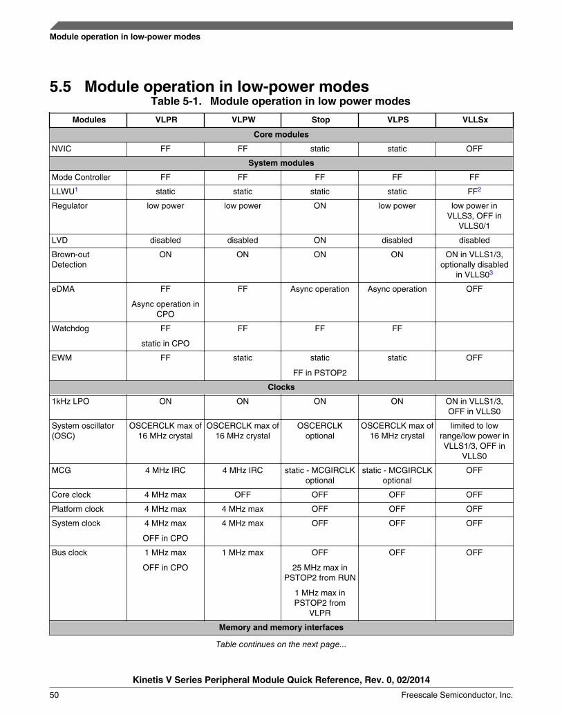
5.5 Module operation in low-power modesTable 5-1. Module operation in low power modes
Modules VLPR VLPW Stop VLPS VLLSx
Core modules
NVIC FF FF static static OFF
System modules
Mode Controller FF FF FF FF FF
LLWU1 static static static static FF2
Regulator low power low power ON low power low power inVLLS3, OFF in
VLLS0/1
LVD disabled disabled ON disabled disabled
Brown-outDetection
ON ON ON ON ON in VLLS1/3,optionally disabled
in VLLS03
eDMA FF
Async operation inCPO
FF Async operation Async operation OFF
Watchdog FF
static in CPO
FF FF FF
EWM FF static static
FF in PSTOP2
static OFF
Clocks
1kHz LPO ON ON ON ON ON in VLLS1/3,OFF in VLLS0
System oscillator(OSC)
OSCERCLK max of16 MHz crystal
OSCERCLK max of16 MHz crystal
OSCERCLKoptional
OSCERCLK max of16 MHz crystal
limited to lowrange/low power inVLLS1/3, OFF in
VLLS0
MCG 4 MHz IRC 4 MHz IRC static - MCGIRCLKoptional
static - MCGIRCLKoptional
OFF
Core clock 4 MHz max OFF OFF OFF OFF
Platform clock 4 MHz max 4 MHz max OFF OFF OFF
System clock 4 MHz max
OFF in CPO
4 MHz max OFF OFF OFF
Bus clock 1 MHz max
OFF in CPO
1 MHz max OFF
25 MHz max inPSTOP2 from RUN
1 MHz max inPSTOP2 from
VLPR
OFF OFF
Memory and memory interfaces
Table continues on the next page...
Module operation in low-power modes
Kinetis V Series Peripheral Module Quick Reference, Rev. 0, 02/2014
50 Freescale Semiconductor, Inc.
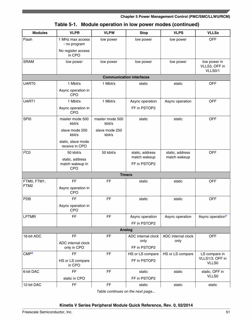
Table 5-1. Module operation in low power modes (continued)
Modules VLPR VLPW Stop VLPS VLLSx
Flash 1 MHz max access- no program
No register accessin CPO
low power low power low power OFF
SRAM low power low power low power low power low power inVLLS3, OFF in
VLLS0/1
Communication interfaces
UART0 1 Mbit/s
Async operation inCPO
1 Mbit/s static static OFF
UART1 1 Mbit/s
Async operation inCPO
1 Mbit/s Async operation
FF in PSTOP2
Async operation OFF
SPI0 master mode 500kbit/s
slave mode 250kbit/s
static, slave modereceive in CPO
master mode 500kbit/s
slave mode 250kbit/s
static static OFF
I2C0 50 kbit/s
static, addressmatch wakeup in
CPO
50 kbit/s static, addressmatch wakeup
FF in PSTOP2
static, addressmatch wakeup
OFF
Timers
FTM0, FTM1,FTM2
FF
Async operation inCPO
FF static static OFF
PDB FF
Async operation inCPO
FF static static OFF
LPTMR FF FF Async operation
FF in PSTOP2
Async operation Async operation4
Analog
16-bit ADC FF
ADC internal clockonly in CPO
FF ADC internal clockonly
FF in PSTOP2
ADC internal clockonly
OFF
CMP5 FF
HS or LS comparein CPO
FF HS or LS compare
FF in PSTOP2
HS or LS compare LS compare inVLLS1/3, OFF in
VLLS0
6-bit DAC FF
static in CPO
FF static
FF in PSTOP2
static static, OFF inVLLS0
12-bit DAC FF FF static static static
Table continues on the next page...
Chapter 5 Power Management Control (PMC/SMC/LLWU/RCM)
Kinetis V Series Peripheral Module Quick Reference, Rev. 0, 02/2014
Freescale Semiconductor, Inc. 51

Table 5-1. Module operation in low power modes (continued)
Modules VLPR VLPW Stop VLPS VLLSx
static in CPO FF in PSTOP2
Human-machine interfaces
GPIO FF
IOPORT write onlyin CPO
FF static output,wakeup input
FF in PSTOP2
static output,wakeup input
OFF, pins latched
1. Using the LLWU module, the external pins available for this chip do not require the associated peripheral function to beenabled. It only requires the function controlling the pin (GPIO or peripheral) to be configured as an input to allow atransition to occur to the LLWU.
2. Since LPO clock source is disabled, filters will be bypassed during VLLS03. The STOPCTRL[PORPO] bit in the SMC module controls this option.4. LPO clock source is not available in VLLS0. To use system OSC in VLLS0 it must be configured for bypass (external
clock) operation. Pulse counting is available in all modes.5. CMP in stop or VLPS supports high speed or low speed external pin-to-pin or external pin-to-DAC compares. CMP in
VLLSx only supports low speed external pin-to-pin or external pin-to-DAC compares. Windowed, sampled & filtered modesof operation are not available while in stop, VLPS, or VLLSx modes.
5.6 Mode transition requirementsThe following table defines triggers for the various state transitions:
Table 5-2. Power mode transition triggers
Transition # From To Trigger conditions
1 RUN WAIT Sleep-now or sleep-on-exit modes entered with SLEEPDEEPclear, controlled in System Control Register in ARM core.
WAIT RUN Interrupt or Reset
2 RUN STOP Sleep-now or sleep-on-exit modes entered with SLEEPDEEPset, which is controlled in System Control Register in ARMcore.
STOP RUN Interrupt or Reset
3 RUN VLPR The core, system, bus and flash clock frequencies arerestricted in this mode.
Set PMPROT[AVLP]=1, PMCTRL[RUNM]=10
VLPR RUN Set PMCTRL[RUNM]=00 or
Reset.
4 VLPR VLPW Sleep-now or sleep-on-exit modes entered with SLEEPDEEPclear, which is controlled in System Control Register in ARMcore.
VLPW VLPR Interrupt
5 VLPW RUN Reset.
Table continues on the next page...
Mode transition requirements
Kinetis V Series Peripheral Module Quick Reference, Rev. 0, 02/2014
52 Freescale Semiconductor, Inc.

Table 5-2. Power mode transition triggers (continued)
Transition # From To Trigger conditions
6 VLPR VLPS PMCTRL[STOPM]=000 If PMCTRL[STOPM]=000 andSTOPCTRL[PSTOPO]=00, then VLPS mode is enteredinstead of STOP. If PMCTRL[STOPM]=000 andSTOPCTRL[PSTOPO]=01 or 10, then only a Partial Stopmode is entered instead of VLPS or 010,
Sleep-now or sleep-on-exit modes entered with SLEEPDEEPset, which is controlled in System Control Register in ARMcore.
VLPS VLPR Interrupt
NOTE: If VLPS was entered directly from RUN, hardwarewill not allow this transition and will force exit back toRUN
7 RUN VLPS PMPROT[AVLP]=1, PMCTRL[STOPM]=010,
Sleep-now or sleep-on-exit modes entered with SLEEPDEEPset, which is controlled in System Control Register in ARMcore.
VLPS RUN Interrupt and set PMCTRL[RUNM]=00, transitioning to RUNbefore entering VLPS or
Reset.
8 RUN VLLSx PMPROT[AVLLS]=1, PMCTRL[STOPM]=100,STOPCTRL[VLLSM]=x (VLLSx), Sleep-now or sleep-on-exitmodes entered with SLEEPDEEP set, which is controlled inSystem Control Register in ARM core.
VLLSx RUN Wake up from enabled LLWU LPTMR input source or RESETpin
9 VLPR VLLSx PMPROT[AVLLS]=1, PMCTRL[STOPM]=100,STOPCTRL[VLLSM]=x (VLLSx), Sleep-now or sleep-on-exitmodes entered with SLEEPDEEP set, which is controlled inSystem Control Register in ARM core.
5.7 Source of wake-up, pins, and modulesTable 5-3. Source of wake-up, pins, and modules
LLWU pin Module source or pin name
LLWU_P3 PTA4
LLWU_P5 PTB0
LLWU_P6 PTC1
LLWU_P7 PTC3
LLWU_P8 PTC4
LLWU_P9 PTC5
LLWU_P10 PTC6
LLWU_P12 PTD0
Table continues on the next page...
Chapter 5 Power Management Control (PMC/SMC/LLWU/RCM)
Kinetis V Series Peripheral Module Quick Reference, Rev. 0, 02/2014
Freescale Semiconductor, Inc. 53

Table 5-3. Source of wake-up, pins, and modules (continued)
LLWU pin Module source or pin name
LLWU_P13 PTD2
LLWU_P14 PTD4
LLWU_P15 PTD6
LLWU_M0IF LPTMR0
LLWU_M1IF CMP0
LLWU_M2IF CMP1
LLWU_M3IF Reserved
LLWU_M4IF Reserved
LLWU_M5IF Reserved
LLWU_M6IF Reserved
LLWU_M7IF Reserved
Source of wake-up, pins, and modules
Kinetis V Series Peripheral Module Quick Reference, Rev. 0, 02/2014
54 Freescale Semiconductor, Inc.

Chapter 6enhanced Direct Memory Access (eDMA) Controller
6.1 eDMA
6.1.1 Overview
This chapter is a compilation of code examples and quick reference materials created toshorten the development time of your applications that use the eDMA controller of theKinetis V series. Consult the device-specific reference manual for specific partinformation.
This chapter demonstrates how to configure and use the eDMA controller to create datamovement between different memory and peripheral spaces without CPU intervention.
6.1.2 Introduction
The eDMA controller provides the ability to move data from one memory mappedlocation to another. After it is configured and initiated, the eDMA controller operates inparallel to the core, performing data transfers that would otherwise have been handled bythe CPU. This results in reduced CPU loading and a corresponding increase in systemperformance. Figure 6-1 illustrates the functionality provided by the eDMA controller.
Kinetis V Series Peripheral Module Quick Reference, Rev. 0, 02/2014
Freescale Semiconductor, Inc. 55
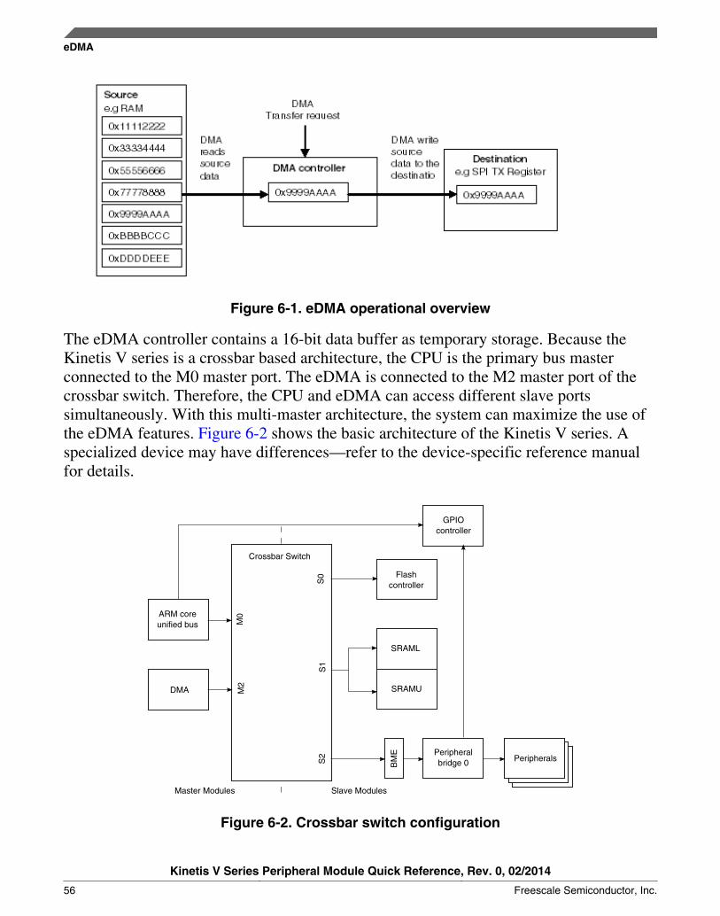
Figure 6-1. eDMA operational overview
The eDMA controller contains a 16-bit data buffer as temporary storage. Because theKinetis V series is a crossbar based architecture, the CPU is the primary bus masterconnected to the M0 master port. The eDMA is connected to the M2 master port of thecrossbar switch. Therefore, the CPU and eDMA can access different slave portssimultaneously. With this multi-master architecture, the system can maximize the use ofthe eDMA features. Figure 6-2 shows the basic architecture of the Kinetis V series. Aspecialized device may have differences—refer to the device-specific reference manualfor details.
ARM coreunified bus
DMA
Crossbar Switch
GPIOcontroller
Flashcontroller
SRAML
SRAMU
BM
E Peripheralbridge 0 PeripheralsS
2S
1S
0
M0
M2
Master Modules Slave Modules
Figure 6-2. Crossbar switch configuration
eDMA
Kinetis V Series Peripheral Module Quick Reference, Rev. 0, 02/2014
56 Freescale Semiconductor, Inc.

The crossbar switch forms the heart of this multi-master architecture. It links each masterto the required slave device. Both fixed priority and round robin arbitration schemes areavailable. If both masters attempt joint access to the same slave, an arbitration schemebegins and eliminates bus contention.
6.2 eDMA triggerEach channel of the Kinetis eDMA controller can be configured to begin DMA transfersfrom multiple peripheral sources or software. The eDMA controller integrates the DMAMux to route a different trigger source to the 16 channels. With the DMA Mux, up to 63events occurring within other peripheral modules can activate an eDMA transfer. Inmany modules, event flags can be asserted as either eDMA or Interrupt requests. Thesesources can be selected through DMAMUX_CHCFGn[SOURCE] registers. However,different devices may have different peripheral source configurations. Refer to thedevice-specific reference manual for details.
6.2.1 DMA multiplexer
The eDMA channel multiplexer routes the eDMA trigger source. The 52 peripheral slotsand 10 always-on slots can be routed to the 16 channels. Each channel router can beassigned to one of the 52 possible peripheral DMA slots or to one of the 10 always-onslots.
Chapter 6 enhanced Direct Memory Access (eDMA) Controller
Kinetis V Series Peripheral Module Quick Reference, Rev. 0, 02/2014
Freescale Semiconductor, Inc. 57
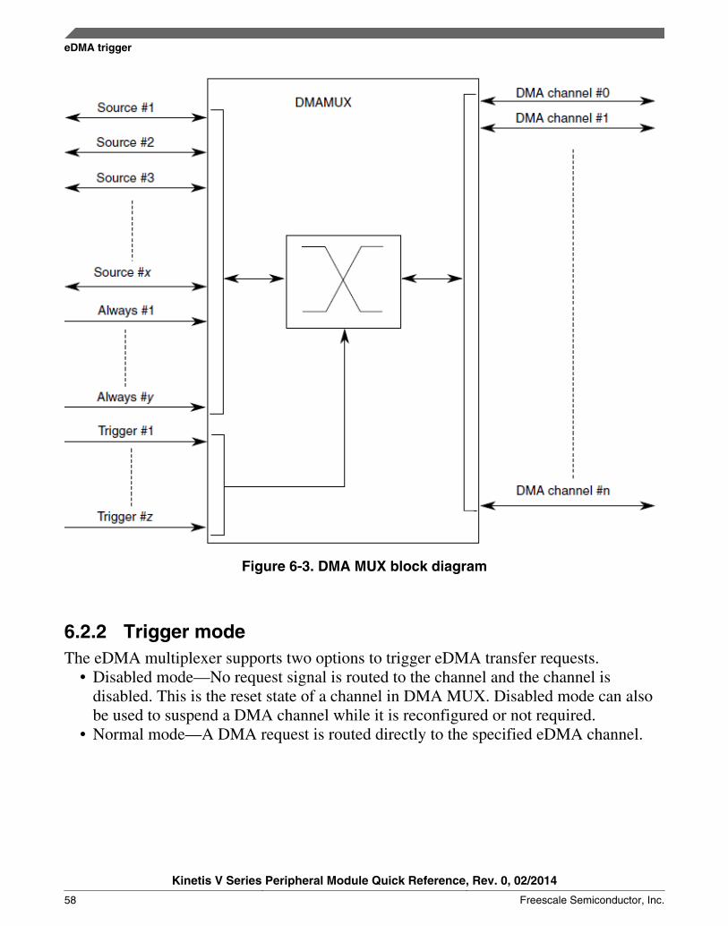
Figure 6-3. DMA MUX block diagram
6.2.2 Trigger modeThe eDMA multiplexer supports two options to trigger eDMA transfer requests.
• Disabled mode—No request signal is routed to the channel and the channel isdisabled. This is the reset state of a channel in DMA MUX. Disabled mode can alsobe used to suspend a DMA channel while it is reconfigured or not required.
• Normal mode—A DMA request is routed directly to the specified eDMA channel.
eDMA trigger
Kinetis V Series Peripheral Module Quick Reference, Rev. 0, 02/2014
58 Freescale Semiconductor, Inc.

6.2.3 Multiple transfer requests
Only one channel can actively perform a transfer. To manage multiple pending transferrequests, the eDMA controller offers channel prioritization. Fixed priority or round robinpriority can be selected.
In the fixed priority scheme each channel is assigned a priority level. When multiplerequests are pending, the channel with the highest priority level performs its transfer first.By default, fixed priority arbitration is implemented with each channel being assigned apriority level equal to its channel number. Higher priority channels can preempt lowerpriority channels. Preemption occurs when a channel is performing a transfer while atransfer request is asserted to a channel of a higher priority. The lower priority channelhalts its transfer on completion of the current read/write operation and enables thechannel of higher priority to work.
In round robin mode, the eDMA cycles through the channels from the highest to thelowest, checking for a pending request. When a channel with a pending request isreached, it is allowed to perform its transfer. After the transfer has been completed, theeDMA continues to cycle through the channels looking for the next pending request.
6.3 Transfer processEach channel requires a 32-byte transfer control descriptor (TCD) for defining the desireddata movement operation. The channel descriptors are stored in the eDMA local memoryin sequential order.
Each time a channel is activated and executes, n bytes are transferred from the source tothe destination. This is referred to as a minor transfer loop. A major transfer loop consistsof a number of minor transfer loops, and this number is specified within the TCD. Asiterations of the minor loop are completed, the current iteration (CITER) TCD field isdecremented. When the current iteration field has been exhausted, the channel hascompleted a major transfer loop. This figure shows the relationship between major andminor loops. In this example a channel is configured so that a major loop consists of threeiterations of a minor loop. The minor loop is configured as a transfer of 4 bytes.
Chapter 6 enhanced Direct Memory Access (eDMA) Controller
Kinetis V Series Peripheral Module Quick Reference, Rev. 0, 02/2014
Freescale Semiconductor, Inc. 59
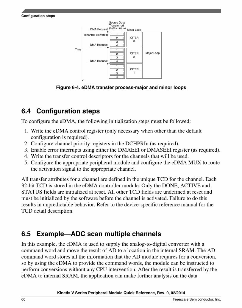
1 2 3 4
CITER
3
1 2 3 4
CITER
2
1 2 3 4
CITER
1
Major Loop
DMA Request
(channel activated)
DMA Request
DMA Request
Time
Source Data Transferred (bytes - n) =4 Minor Loop
Figure 6-4. eDMA transfer process-major and minor loops
6.4 Configuration stepsTo configure the eDMA, the following initialization steps must be followed:
1. Write the eDMA control register (only necessary when other than the defaultconfiguration is required).
2. Configure channel priority registers in the DCHPRIn (as required).3. Enable error interrupts using either the DMAEEI or DMASEEI register (as required).4. Write the transfer control descriptors for the channels that will be used.5. Configure the appropriate peripheral module and configure the eDMA MUX to route
the activation signal to the appropriate channel.
All transfer attributes for a channel are defined in the unique TCD for the channel. Each32-bit TCD is stored in the eDMA controller module. Only the DONE, ACTIVE andSTATUS fields are initialized at reset. All other TCD fields are undefined at reset andmust be initialized by the software before the channel is activated. Failure to do thisresults in unpredictable behavior. Refer to the device-specific reference manual for theTCD detail description.
6.5 Example—ADC scan multiple channelsIn this example, the eDMA is used to supply the analog-to-digital converter with acommand word and move the result of AD to a location in the internal SRAM. The ADcommand word stores all the information that the AD module requires for a conversion,so by using the eDMA to provide the command words, the module can be instructed toperform conversions without any CPU intervention. After the result is transferred by theeDMA to internal SRAM, the application can make further analysis on the data.
Configuration steps
Kinetis V Series Peripheral Module Quick Reference, Rev. 0, 02/2014
60 Freescale Semiconductor, Inc.

6.5.1 Module configuration
To implement this example two eDMA channels are required: one to transfer thecommand word and the other to transfer the result. The command transfer requests asoftware trigger by setting the START bit of channel 1, and an always-on trigger.Channel 1 is configured to perform this transfer.
Channel 0 is used to transfer the AD result to RAM. This transfer is activated when theAD result ready flag is asserted, and after transfer is complete. Link to channel0 totransfer the next command to the ADC SC1 register, until all channels completeconversion and BITER counter is equal to 0, generate eDMA interrupt request.
The following code provides the eDMA driver and defines the eDMA structure tocomplete the configuration.
sDMAConfig.Channel = 1; sDMAConfig.Slot = DMA_SLOTS_ALWAYS_EN; /* always on */ sDMAConfig.sSetting.bIntEn = TRUE; sDMAConfig.sSetting.bDebugEn = TRUE; sDMAConfig.sSetting.bRoundRobinEn = TRUE; sDMAConfig.sSetting.bReqEn = FALSE; sTCDInfo.SADDR = (uint32_t)&u32ADCChannel[0]; sTCDInfo.SOFF = sizeof(u32ADCChannel[0]); sTCDInfo.ATTR = DMA_ATTR_SMOD(0)| DMA_ATTR_SSIZE(2)| DMA_ATTR_DSIZE(2)| DMA_ATTR_DMOD(0) ; sTCDInfo.NBYTES_MLNO = sizeof(u32ADCChannel[0]); sTCDInfo.DADDR = (uint32_t)&ADC0->SC1[0]; sTCDInfo.DOFF = 0; sTCDInfo.BITER_ELINKNO= DMA_BITER_ELINKYES_BITER(ADC_CHANNEL_NUMBERS) sTCDInfo.CITER_ELINKNO = sTCDInfo.BITER_ELINKNO; sTCDInfo.SLAST = -(sizeof(u32ADCChannel[0])*ADC_CHANNEL_NUMBERS); sTCDInfo.CSR = DMA_CSR_INTMAJOR_MASK; sDMAConfig.sTCDInfo = sTCDInfo; /* Initialize the eDMA channel1 to transfer channel value to ADC_SC1 */ DMA_Init(DMA0,&sDMAConfig); sDMAConfig.Channel = 0; sDMAConfig.Slot = DMA_SLOTS_ADC0; /* ADC0 request */ sDMAConfig.sSetting.bReqEn = TRUE;
sTCDInfo1.SADDR = (uint32_t)&ADC0->R[0]; sTCDInfo1.SOFF = 0; sTCDInfo1.ATTR = DMA_ATTR_SMOD(0)| DMA_ATTR_SSIZE(2)| DMA_ATTR_DSIZE(2)| DMA_ATTR_DMOD(0) ; sTCDInfo1.NBYTES_MLNO = sizeof(u32ADCResult[0]); sTCDInfo1.DADDR = (uint32_t)&u32ADCResult[0]; sTCDInfo1.DOFF = sizeof(u32ADCResult[0]); sTCDInfo1.BITER_ELINKYES = DMA_BITER_ELINKYES_BITER(ADC_CHANNEL_NUMBERS) |DMA_BITER_ELINKYES_ELINK_MASK |DMA_BITER_ELINKYES_LINKCH(1) ;
Chapter 6 enhanced Direct Memory Access (eDMA) Controller
Kinetis V Series Peripheral Module Quick Reference, Rev. 0, 02/2014
Freescale Semiconductor, Inc. 61

sTCDInfo1.CITER_ELINKYES = sTCDInfo1.BITER_ELINKYES; sTCDInfo1.DLAST_SGA = -(sizeof(u32ADCResult[0])*ADC_CHANNEL_NUMBERS); sTCDInfo1.CSR = DMA_CSR_INTMAJOR_MASK; sDMAConfig.sTCDInfo = sTCDInfo1; /* Initialize the eDMA channel0 to transfer ADC result to buffer */ DMA_Init(DMA0,&sDMAConfig); DMA_SetCallBack(DMA_Ch0Task,0); NVIC_EnableIRQ(DMA0_IRQn); DMA_SetCallBack(DMA_Ch1Task,1); NVIC_EnableIRQ(DMA1_IRQn);
/* Set eDMA channel 0 "START" bit, launch ADC conversion */ DMA_SetSTARTbit(DMA0,0x1);
Using the above configurations, the required DMA functionality for this example hasbeen achieved.
Example—ADC scan multiple channels
Kinetis V Series Peripheral Module Quick Reference, Rev. 0, 02/2014
62 Freescale Semiconductor, Inc.

Chapter 7Universal Asynchronous Receiver and Transmitter(UART) Module
7.1 OverviewThe UART module on the Kinetis V series devices supports asynchronous, full-duplexserial communications with peripheral devices or other CPUs. The UART module hasfour main modes of operation -- UART, IrDA, and LIN mode.
The following sections will discuss the features and use of the UART in UART mode. Inparticular the use of the UART as an RS-232 serial communication port will bedescribed. For full details on the UART module, including all of its features and modesof operation, please see the device-specific reference manual.
7.2 FeaturesThe feature set available on the UARTs vary from UART to UART. Basic UARTfunctionality is available on all UARTs, but the clock source for the module and thetransmit and receive FIFO sizes can vary. The UART intantiation table lists the UARTfeatures that vary based on UART module instantiation.
Table 7-1. UART instantiations on Kinetis
UART instance LIN supported? FIFOs Module clock
UART0 Yes 8 entry TxFIFO, 8 entryRxFIFO
Core clock
UART1 Yes 8 entry TxFIFO, 8 entryRxFIFO
Peripheral clock
NOTEThis table describes the UART instantiations on the Kinetis Vseries devices available at the time of publication. As new
Kinetis V Series Peripheral Module Quick Reference, Rev. 0, 02/2014
Freescale Semiconductor, Inc. 63

Kinetis devices become available the UART instantiationsmight change. See the Chip Configuration chapter of thedevice-specific reference manual to verify the UARTinstantiation information for your device.
7.3 Configuration exampleThe examples included here poll UART status flags to determine when receive data isavailable or when transmit data can be written into the FIFO. This approach is the mostCPU intensive, but it is often the most practical approach when handling small messages.As message sizes increase it might be useful to use interrupts or the eDMA to decreasethe CPU loading. However, the overhead required to set up the interrupts or eDMA mustbe taken into account. If the additional overhead outweighs the reduction in CPU loading,then polling is the best approach.
Using the UART interrupts to signal the CPU that data can be read from or written to theUART will help to decrease the CPU loading. The UART has a number of status anderror interrupt flags that can be used, but for typical receive and transmit operations thereceive data register full flag (UARTx_S1[RDRF]) and transmit data register empty flag(UARTx_S1[TDRE]) are enabled using the UARTx_C2[TIE, RIE] bits. The names ofthese flags are misleading, because they do not always indicate a full or empty condition.For UARTs that include a FIFO, the full or empty condition is determined based on theamount of data in the FIFO compared to a programmable watermark. If both the RDRFand TDRE interrupt requests are enabled, then the UART interrupt handler needs to readthe S1 register to determine which condition is true then read and/or write to the UARTdata register (UARTx_D) to clear the flags. Because the CPU is responsible for movingdata there is CPU loading associated with an interrupt-driven software approach.
Using the eDMA to move data minimizes CPU loading even more than using the UARTinterrupts. The UART's same RDRF and TDRE flags used for an interrupt drivensoftware approach can be re-routed to the eDMA controller instead. This is done bysetting the UARTx_C5[TDMAS, RDMAS] bits. Each of these requests are routed to adifferent eDMA channel (the specific eDMA channels are selected by programming theeDMA channel mux). One eDMA channel is responsible for handling receive traffic, so itreads one or more bytes from the UART for each request. The second eDMA channel isresponsible for handling the transmit traffic, so it writes one or more bytes to the UARTfor each request. When the entire transmit or receive eDMA movement is complete theeDMA can interrupt the core to notify it of the completion. In this approach the CPU hasno loading associated with the actual data movement. All of the CPU loading is the result
Configuration example
Kinetis V Series Peripheral Module Quick Reference, Rev. 0, 02/2014
64 Freescale Semiconductor, Inc.

of the initial configuration of both the UART and eDMA modules and then anyprocessing of data that is required to prepare it for transmission or interpret it afterreception.
7.3.1 UART initialization example
The initialization code provided in this section can be used to configure the UART for 8-N-1 operation (eight data bits, no parity, and one stop bit) with interrupts and hardwareflow-control disabled. The parameters passed into this function are the UART channels toinitialize (uartch), the module clock frequency for the UART in kHz (sysclk), and thedesired baud rate for communication (baud).
NOTEThe UART modules are pinned out in multiple locations, so theinitialization function below doesn't know which UART pins toenable. The desired UART pins should be enabled beforecalling this initialization function.
void UART_Init(UART_Type *pUART, UART_ConfigType *pConfig){ uint16_t u16Sbr, u16Brfa; uint8_t u8Temp; uint32_t u32SysClk = pConfig ≥ u32SysClkHz; uint32_t u32Baud = pConfig ≥ u32Baudrate;
/* Sanity check */ ASSERT((pUART == UART0) || (pUART == UART1)); /* Enable the clock to the selected UART */ if (pUART == UART0) { SIM->SCGC4 |= SIM_SCGC4_UART0_MASK; } if (pUART == UART1) { SIM->SCGC4 |= SIM_SCGC4_UART1_MASK; } /* Ensure the transmitter and receiver are disabled when changing settings*/ pUART -> C2 & = ~(UART_C2_TE_MASK | UART_C2_RE_MASK ); /* Configure the UART for 8-bit mode, no parity */ pUART -> C1 = 0; /* Calculate baud settings */ //u16Sbr = (((u32SysClk) >> 4) + (u32Baud >> 1))/u32Baud; u16Sbr = (uint16)((((u32SysClk*1000) >> 4))/u32Baud); /* Save off the current value of the UARTx_BDH except for the SBR field */ u8Temp = pUART -> BDH & ~(UART_BDH_SBR_MASK); pUART -> BDH = u8Temp | UART_BDH_SBR(((u16Sbr & 0x1F00) >> 8)); pUART -> BDL = (uint8_t)(u16Sbr & UART_BDL_SBR_MASK); /* Determine if a fractional divider is needed to get closer to the baud rate */ u16Brfa = (((u32SysClk*32000)/(u32Baud * 16)) - (u16Sbr * 32));
Chapter 7 Universal Asynchronous Receiver and Transmitter (UART) Module
Kinetis V Series Peripheral Module Quick Reference, Rev. 0, 02/2014
Freescale Semiconductor, Inc. 65

/* Save off the current value of the UARTx_C4 register except for the BRFA field */ u8Temp = pUART -> C4 & ~(UART_C4_BRFA(0x1F)); pUART -> C4 = u8Temp | UART_C4_BRFA(u16Brfa);
/* Enable receiver and transmitter */ pUART -> C2 |= (UART_C2_TE_MASK | UART_C2_RE_MASK );}
The initialization above can be simplified to the following steps:
1. Enable the UART pins by configuring the appropriate PORTx_PCRn registers (notshown in the code example).
2. Enable the clock to the UART module.3. Disable the transmitter and receiver. This step is included to ensure that the UART is
not active when it is being configured. This step is not needed if the uart_initfunction is always called when the UART is already in a disabled state (the UART isdisabled after reset by default).
4. Configure the UART control registers for the desired format. For 8-N-1 operation noUART registers need to be configured (the default register settings configure theUART for 8-N-1 operation).
5. Calculate the baud rate dividers. This includes calculating the 13-bit whole numberbaud rate divider, the SBR field stored in the UARTx_BDH and UARTx_BDLregisters, and the 5-bit fractional baud rate divider, the UARTx_C4[BRFA] field.
6. Enable the transmitter and receiver to start the UART.
7.3.2 UART receive example
The function below shows an implementation for a simple polled UART receivefunction. The parameter passed into this function is the UART channel to receive acharacter (uartch). The function returns the character that is received.
uint8_t UART_GetChar(UART_Type *pUART){ /* Sanity check */ ASSERT((pUART == UART0) || (pUART == UART1)); /* Wait until character has been received */ while (!(pUART ≥ S1 & UART_S1_RDRF_MASK)); /* Return the 8-bit data from the receiver */ return pUART ≥ D;}
Because this is a polled implementation, the function will wait until a character isreceived. If no character is received, then the code will remain in the while loopindefinitely. To avoid code getting stuck when no traffic is being received, include afunction to test whether a character is present. The uart_getchar_present function can becalled prior to calling the uart_getchar function in cases when UART receive traffic is notguaranteed or required before moving on with program execution.
Configuration example
Kinetis V Series Peripheral Module Quick Reference, Rev. 0, 02/2014
66 Freescale Semiconductor, Inc.

int UART_GetChar_Present (UART_Type *pUART){ return (pUART ≥ S1 & UART_S1_RDRF_MASK);}
7.3.3 UART transmit example
This function is an implementation for a simple polled UART transmit function. Theparameters passed into this function are the UART channel that will be used to transmit(uartch) and the character to be sent (ch).
void UART_PutChar(UART_Type *pUART, uint8_t u8Char){ /* Wait until space is available in the FIFO */ while (!(pUART ≥ S1 & UART_S1_TDRE_MASK)); /* Send the character */ pUART ≥ D = (uint8_t)u8Char;}
7.3.4 UART configuration for interrupts or DMA requests
The examples included here poll UART status flags to determine when receive data isavailable or when transmit data can be written into the FIFO. This approach is the mostCPU intensive, but it is often the most practical approach when handling small messages.As message sizes increase it might be useful to use interrupts or the DMA to decrease theCPU loading. However, the overhead required to set up the interrupts or DMA should betaken into account. If the additional overhead outweighs the reduction in CPU loading,then polling is the best approach.
Using the UART interrupts to signal the CPU that data can be read from or written to theUART will help to decrease the CPU loading. The UART has a number of status anderror interrupt flags that can be used, but for typical receive and transmit operations thereceive data register full flag (UARTx_S1[RDRF]) and transmit data register empty flag(UARTx_S1[TDRE]) would be enabled using the UARTx_C2[TIE, RIE] bits. The namesof these flags are a bit misleading, since they don't always indicate a full or emptycondition. For UARTs that include a FIFO, the full or empty condition is determinedbased on the amount of data in the FIFO compared to a programmable watermark. If boththe RDRF and TDRE interrupt requests are enabled, then the UART interrupt handlerwould need to read the S1 register to determine which condition is true then read and/orwrite to the UART data register (UARTx_D) to clear the flags. Since the CPU is stillresponsible for moving data there is CPU loading associated with an interrupt-drivensoftware approach.
Chapter 7 Universal Asynchronous Receiver and Transmitter (UART) Module
Kinetis V Series Peripheral Module Quick Reference, Rev. 0, 02/2014
Freescale Semiconductor, Inc. 67

Using the DMA to move data can help to decrease the CPU loading even more than usingthe UART interrupts. The UART's same RDRF and TDRE flags used for an interrupt-driven software approach can be re-routed to the eDMA controller instead. This is doneby setting the UARTx_C5[TDMAS, RDMAS] bits. Each of these requests would berouted to a different eDMA channel (the specific eDMA channels would be selected byprogramming the DMA channel mux). One eDMA channel would be responsible forhandling receive traffic, so it would read one or more bytes from the UART for eachrequest. The second eDMA channel would be responsible for handling the transmittraffic, so it would write one or more bytes to the UART for each request. When theentire transmit or receive DMA movement is complete the eDMA can interrupt the coreto notify it of the completion. In this approach the CPU has no loading associated withthe actual data movement. All of the CPU loading is the result of the initial configurationof both the UART and eDMA modules and then any processing of data that is required toprepare it for transmission or interpret it after reception.
7.4 UART RS-232 hardware implementationThis block diagram illustrates the hardware connections for an RS-232 implementation.The diagram shows the optional hardware flow control signals, but only the RX and TXdata connections are required.
Figure 7-1. UART RS-232 hardware connections block diagram
UART RS-232 hardware implementation
Kinetis V Series Peripheral Module Quick Reference, Rev. 0, 02/2014
68 Freescale Semiconductor, Inc.

Chapter 8Memory-Mapped Divide and Square Root (MMDVSQ)
8.1 IntroductionThe ARM v6M instruction set architecture (ISA) implemented on the Cortex-M0+ coredoes not support integer divide instructions or square root functions. However, thesearithmetic operations are widely used in motor control applications. To maximize suchsystem performance and minimize the device power dissipation, the co-processorMMDVSQ is included in Kinetis V series to support execution of the integer divide andunsigned integer square root operations. The supported integer divide operations include32/32 signed (SDIV) and unsigned (UDIV) calculation.
8.2 FeaturesThe supported features of the MMDVSQ are as follows:
• Lightweight implementation of 32-bit integer divide and square root arithmeticoperations
• Supports 32/32 signed and unsigned divide (or remainder) calculations• Supports 32-bit unsigned square root calculations
• Simple programming model includes input data and result registers plus a control/status register
• Programming model interface optimized for activation from inline code or softwarelibrary call
• “Fast Start” configuration minimizes the memory-mapped register writeoverhead
• Supports two methods to determine when result is valid, including softwarepolling
• Configurable divide-by-zero response
Kinetis V Series Peripheral Module Quick Reference, Rev. 0, 02/2014
Freescale Semiconductor, Inc. 69

• Memory-mapped AHB coprocessor based at 0xF000_4000 address space reservedfor CPU devices
• Pipelined design processes 2 bits per cycle with early termination exit for minimumexecution time
8.3 MMDVSQ in Cortex-M0+ core platformThe generic core platform diagram illustrates the location of the MMDVSQ modulewithin the Cortex-M0+ platform.
AXBS
s1
s2
m0
s0
FMC
LD/ST
Dbg
NVIC
Fetch
Cortex-M0+ Core
MTB PortAHB Bus
m2
AGU
MUL
RAMArray
32
Dec Rn
SHFTALU
DMA_4ch
NVMArray
PRAM32
RGPIO
PBRIDGEBME32
IO Port
SlavePeripherals
Alt-Master m3
-Lite
MMDVSQ
MTBMCM
Figure 8-1. Generic Cortex-M0+ Core Platform Block Diagram
All functionality associated with the MMDVSQ module resides in the core platform’sclock domain. The MMDVSQ is only clocked when responding to bus requests to itsprogramming model or is busy performing a calculation. This minimizes system powerdissipation.
8.4 MMDVSQ programming modelThere are four 32-bit memory mapped registers and one status and control register:
MMDVSQ in Cortex-M0+ core platform
Kinetis V Series Peripheral Module Quick Reference, Rev. 0, 02/2014
70 Freescale Semiconductor, Inc.
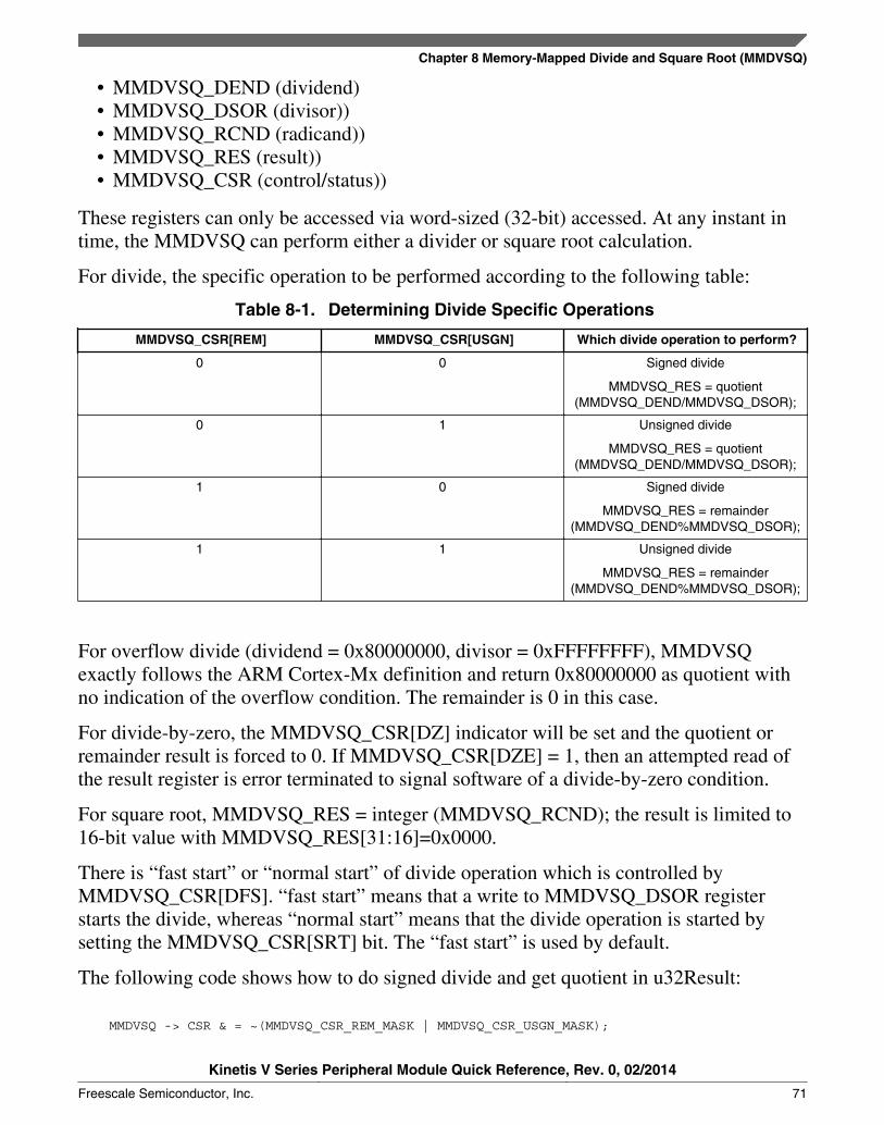
• MMDVSQ_DEND (dividend)• MMDVSQ_DSOR (divisor))• MMDVSQ_RCND (radicand))• MMDVSQ_RES (result))• MMDVSQ_CSR (control/status))
These registers can only be accessed via word-sized (32-bit) accessed. At any instant intime, the MMDVSQ can perform either a divider or square root calculation.
For divide, the specific operation to be performed according to the following table:
Table 8-1. Determining Divide Specific Operations
MMDVSQ_CSR[REM] MMDVSQ_CSR[USGN] Which divide operation to perform?
0 0 Signed divide
MMDVSQ_RES = quotient(MMDVSQ_DEND/MMDVSQ_DSOR);
0 1 Unsigned divide
MMDVSQ_RES = quotient(MMDVSQ_DEND/MMDVSQ_DSOR);
1 0 Signed divide
MMDVSQ_RES = remainder(MMDVSQ_DEND%MMDVSQ_DSOR);
1 1 Unsigned divide
MMDVSQ_RES = remainder(MMDVSQ_DEND%MMDVSQ_DSOR);
For overflow divide (dividend = 0x80000000, divisor = 0xFFFFFFFF), MMDVSQexactly follows the ARM Cortex-Mx definition and return 0x80000000 as quotient withno indication of the overflow condition. The remainder is 0 in this case.
For divide-by-zero, the MMDVSQ_CSR[DZ] indicator will be set and the quotient orremainder result is forced to 0. If MMDVSQ_CSR[DZE] = 1, then an attempted read ofthe result register is error terminated to signal software of a divide-by-zero condition.
For square root, MMDVSQ_RES = integer (MMDVSQ_RCND); the result is limited to16-bit value with MMDVSQ_RES[31:16]=0x0000.
There is “fast start” or “normal start” of divide operation which is controlled byMMDVSQ_CSR[DFS]. “fast start” means that a write to MMDVSQ_DSOR registerstarts the divide, whereas “normal start” means that the divide operation is started bysetting the MMDVSQ_CSR[SRT] bit. The “fast start” is used by default.
The following code shows how to do signed divide and get quotient in u32Result:
MMDVSQ -> CSR & = ~(MMDVSQ_CSR_REM_MASK | MMDVSQ_CSR_USGN_MASK);
Chapter 8 Memory-Mapped Divide and Square Root (MMDVSQ)
Kinetis V Series Peripheral Module Quick Reference, Rev. 0, 02/2014
Freescale Semiconductor, Inc. 71

MMDVSQ -> DEND = i32Numerator; MMDVSQ -> DSOR = i32Denominator; u32Result = MMDVSQ -> RES;
The following code shows how to do signed divide and get remainder in u32Result:
MMDVSQ -> CSR = (MMDVSQ ≥ CSR & ~(MMDVSQ_CSR_USGN_MASK)) | MMDVSQ_CSR_REM_MASK; MMDVSQ -> DEND = i32Numerator; MMDVSQ -> DSOR = i32Denominator; i32Result = MMDVSQ -> RES;
The following code shows how to get the square root of u32Data in u16Result:
MMDVSQ -> RCND = u32Data; u16Result = MMDVSQ -> RES;
8.5 Square root using Q notation for fractional dataFor the unsigned fractional data using u(nsigned)Qm.n notation, it requires m+n bits (m+n = 32) for the input radicand. The uQm.n format produces a uQ(m/2).(n/2) square root.
For example, Π in uQ02.30 format is 0xC90FDAA0. To obtain √Π, MMDVSQ_RCND= 0xC90FDAA0, and the result of its square root is 0x0000E2DF which is 1.7724304199when interpreted as uQ01.15 format. The error of result is -0.001%.
8.6 Execution timeThe MMDVSQ module includes early termination logic to finish both divide and squareroot calculations as quickly as possible, based on the magnitude of the input operand.Therefore, the execution time for the calculations is data dependent onMMDVSQ_DEND. The execution time is defined from the register write to initiate thecalculation until the result register has been updated and available to read (i.e., time withMMDVSQ_CSR[BUSY]=1).
For both divide and square root operation, the shortest execution time is 1 core cycle, andthe longest is 17 cycles. For example, if MMDVSQ_DEND = 0, then the execution timeis 1 core cycle; if MMDVSQ_DEND = 01xx xxxx xxxx xxxx xxxx xxxx xxxx xxxx inbinary format, then the execution time is 17 core cycles.
For more detail information on the execution time, refer to the reference manual.
Square root using Q notation for fractional data
Kinetis V Series Peripheral Module Quick Reference, Rev. 0, 02/2014
72 Freescale Semiconductor, Inc.

Tips of usage
8.7.1 Tips for minimizing the interrupt latency
A memory read o MMDVSQ_RES register while the calculation is still being performedcauses the access to be stalled via the insertion of bus wait states until the new result isloaded into this register. A stalled bus cycle cannot be interrupted. So if system interruptlatency is a concern, a simple wait loop code shall be added to pollMMDVSQ_CRS[BUSY] before reading the result register. Because the polling code isfully interruptible, the interrupt latency is minimized.
8.7.2 Tips for context save and restore in interrupt
If the last calculation was a zero divide and the divide-by-zero enable is set, then a readof the MMDVSQ_RES register is error terminated. To avoid such error terminationduring a context save, follow the steps below:
1. Read MMDVSQ_DEND, DSOR, and CSR register and save their values2. Clear MMDVSQ_CSR[DZE] bit3. Read MMDVSQ_RES register and save its value
When restoring the context, do not initiate another divide calculation by disabling the“fast start” of divide before reloading the MMDVSQ_DEND, DSOR registers. Followthe steps below:
1. Write 0x00000020 to MMDVSQ_CSR to disable the fast start mechanism2. Reload MMDVSQ_DEND, DSOR, and RES register with their previous saved
values
8.7
Chapter 8 Memory-Mapped Divide and Square Root (MMDVSQ)
Kinetis V Series Peripheral Module Quick Reference, Rev. 0, 02/2014
Freescale Semiconductor, Inc. 73

Tips of usage
Kinetis V Series Peripheral Module Quick Reference, Rev. 0, 02/2014
74 Freescale Semiconductor, Inc.
Chapter 9Analog-to-Digital Converter (ADC)
9.1 OverviewEach sub-family of the Kinetis V series may have a different ADC module. This chapterdescribes the ADC module used in KV1x sub-family. The ADC module is a SAR typewith up to 16-bit resolution. It has two independent ADCs, ADC0 and ADC1. The ADCmodule supports up to 4 pairs of differential inputs and up to 24 single-ended inputs andfeatures a self-calibration mode, automatic compare, and hardware average. The ADCx(x=0, 1) has two conversion result registers, ADCx_RA and ADCx_RB, and completes4-channel samples using a trigger event.
9.2 IntroductionThe ADC module can be configured to single-end mode or differential mode. The Outputis right-justified unsigned format for single-ended modes, and it is 2's complement 16-bitsign extended for differential modes. The single mode has 16-bit, 12-bit, 10-bit and 8-bit.The differential mode includes 16-bit, 13-bit, 11-bit and 9-bit. The MSB is symbolplacement, “1” is negative, and “0” is positive.
Each ADC has 12 external channels from ADCx_SE0 to ADC_SE11 in single-end mode,and ADC0 can be configured 2 pair’s differential mode “ADC0_DP0 and ADC0_DM0”and “ADC0_DP1 ADC0_DM1”, and ADC1 can be configured 2 pair’s differential mode“ADC1_DP1 and ADC1_DM1” and “ADC1_DP2 ADC0_DM2”. There is internaltemperature sensor, Bandgap, VREFH and VREFL channel, it is convenient to testjunction or ambient temperature using integral temperature sensor and it can removetemperature drift error in reference via internal reference channel at any time.
ADC has self-calibration function, the user has to calibrate ADC at beginning of theconversion. Calibration function can remove the offset effectively.
Kinetis V Series Peripheral Module Quick Reference, Rev. 0, 02/2014
Freescale Semiconductor, Inc. 75
ADC has hardware average function, it can be set to 4, 8,16 and 32 samples average.Automatic compare function has less-than, greater-than or equal-to, within range, or out-of-range, programmable value.
ADC has low power mode for lower noise application, and long sample selection is goodchoice for low speed and high accuracy operation. ADC also can be configured to highspeed for fast conversion like PMSM motor control application.
ADC has hardware trigger and software trigger mode, ADC can be configured tocontinuous conversion via only one trigger signal.
ADC supports DMA operations, the conversion flag can trigger DMA transfer when theDMA function is enabled.
9.3 Features• 16-bit resolution maximum.• Four pairs of differential and 24 single-ended external analog inputs• Single-ended 16-bit, 12-bit, 10-bit, and 8-bit modes. Differential 16-bit, 13-bit, 11-
bit, and 9-bit modes• Long sample, high speed and low power selection• Conversion complete/hardware average complete flag and interrupt• Asynchronous clock source for lower noise operation with option to output the clock• Hardware or software trigger function• Automatic compare with interrupt for less-than, greater-than or equal-to, within
range, or out-of-range, programmable value• Temperature sensor• Hardware average function• Selectable voltage reference: VREFH/VREFL or VDDA• Self-Calibration mode• Transfers of DMA triggers using COCO flag
9.4 ADC configurationAn initialization procedure is necessary when the user want to get the valid data fromconversion result register, the typical sequence as follows:
1. 1. Enable ADC clock gate.2. ADC calibration, the user can find the details information of calibration on reference
manual 32.4.7 Calibration function.
Features
Kinetis V Series Peripheral Module Quick Reference, Rev. 0, 02/2014
76 Freescale Semiconductor, Inc.

3. Configure ADCx_CFG1 and ADCx_CFG2. Select input clock source, divider, ADCconversion mode, long sample time configuration. Once configure ADCx_CFG1register, the user has to update ADCx_CFG2 register according to ADCx_CFG1configuration.
4. Configure ADCx_SC2 and ADCx_SC3. Select trig mode, compare function and,reference voltage and average function, etc. if compare function is enable,ADCx_CVn register should be correct value.
5. Configure ADCx_SC1n, set up differential or interrupt control bit.6. Write channel number in ADCx_SC1n. If software trigger is enable, it will kick off
ADC conversion.7. Check COCO conversion complete flag.8. Read ADCx_Rn.
The hardware trigger is from PDB module, so the user has to configure PDB module ifhardware is enable. The ADC configuration should be prior to PDB and peripheral. Forexample, if the users want to use FTM channel flag to trig ADC, the user needs toconfigure ADC firstly, secondly configure PDB, FTM is configured at last. It is order todo not neglect the trigger when ADC or PDB is not ready.
9.5 ADC hardware design considerationsThere are some tips for ADC sample circuit design on PCB. Analog inputs should alsohave low pass filters. The challenge with analog inputs, especially for high resolutionanalog-to-digital conversions, is that the filter design needs to consider the sourceimpedance and sample time rather than a simple cutoff frequency.
This topic cannot be discussed in detail here, but the general concept is that fast sampletimes will require smaller capacitor values and source impedances than slow sampletimes. Higher resolution inputs may require smaller capacitor values and sourceimpedances than lower resolution inputs.
In general, capacitor values can range from 10 pF for high speed conversions to 1 uF forlow speed conversions. Series resistors can range from a few hundred Ohms to 10 kΩ.
Use the following general routing and placement guidelines when laying out a newdesign. These guidelines will help to minimize signal quality problems. The ADCvalidation efforts focused on providing very stable voltage reference planes and groundplanes.
Chapter 9 Analog-to-Digital Converter (ADC)
Kinetis V Series Peripheral Module Quick Reference, Rev. 0, 02/2014
Freescale Semiconductor, Inc. 77

• Use high quality RC components for the anti-aliasing filter. Place this RC filter asclose to the ADC input pins as possible where it can remove the most noise.
• Provide very stable analog ground and voltage planes, both for analog power andvoltage references if full accuracy of the ADC is required.
NoteWhen building an external voltage divider on the ADC inputpin to sample high voltage, choose the voltage divider with thelowest equivalent resistor value, because the ADC inputresistance is only 5K Ω.
ADC hardware design considerations
Kinetis V Series Peripheral Module Quick Reference, Rev. 0, 02/2014
78 Freescale Semiconductor, Inc.

Chapter 10Programmable Delay Block (PDB)
10.1 OverviewThe Programmable Delay Block (PDB) is interconnected with the ADC, CMP, andFTMs. The PDB has a pre-trigger function for ADC and provides an interval interrupt asa 12-bit DAC hardware trigger. Individual PDB pulse-out signals are connected to eachCMP block and used for the sample window. The PDB channel 1 pre-trigger can also beused as an FTM synchronous input.
10.2 IntroductionThe PDB provides the programmable delay time for trigger input source, the PDBinterval trigger provides the hardware trigger for 12-bit DAC, and the PDB pulse out forCMP module. The PDB has pre-trigger and back-to-back operations. When pre-trigger isnot enabled, the PDB works under bypass mode.
There are two channels in the PDB. Each channel is associated with one ADC, forexample, channel 0 is assigned to ADC0, and channel 1 is assigned to ADC1. The PDBcan be configured to pre-trigger mode and bypass mode. One PDB channel can beconfigured as two pre-triggers, pre-trigger0 and pre-trigger1, when the input trigger eventis coming, the PDB starts to run, when the PDB counter (the value in PCBx_CNT)matches the channel delay (the value in PDB_CHnDLY0 or PDB_CHnDLY1), thechannel flag will be set, and the trigger can be used as ADC hardware trigger. If the pre-trigger is disabled, it works in bypass mode, the input trigger source of PDB can beconnected to ADC directly.
The PDB pre-trigger back-to-back mode configures the PDB pre-triggers as a singlechain or several chains. PDB back-to-back operation acknowledgment connections areimplemented as follows:
• PDB channel 0 pre-trigger 0 acknowledgement input: ADC1SC1B_COCO
Kinetis V Series Peripheral Module Quick Reference, Rev. 0, 02/2014
Freescale Semiconductor, Inc. 79
• PDB channel 0 pre-trigger1 acknowledgement input: ADC0SC1A_COCO• PDB channel 1 pre-trigger0 acknowledgement input: ADC0SC1B_COCO• PDB channel 1 pre-trigger1 acknowledgement input: ADC1SC1A_COCO
DAC interval trigger can from external hardware trigger: ADC0_SC1A[COCO] flag, orDAC interval trigger, the 16-bit interval time can be set in PDBx_DACINTn[INT]. Theinterval trigger is available once the DAC interval counter matchesPDBx_DACINTn[INT] value.
10.3 FeaturesThe programmable delay block features the following:
• Input hardware trigger sources and one of software trigger source, the user can findPDB input trigger source from chip configuration on KV10 reference manual.
• KV10 has two configurable PDB channels for each ADC.• One PDB channel is associated with one ADC, one trigger output for ADC hardware
trigger and has two pre-trigger outputs for ADC trigger select per PDB channel.• 16-bit delay register per pre-trigger output Trigger outputs, it can be enabled or
disabled independently, and it also support bypass of the delay registers of the pre-trigger outputs, the input trigger event is served to ADC directly.
• PDB can works under One-Shot or Continuous modes.• Optional back-to-back mode operation, which enables the ADC conversions
complete to trigger the next PDB channel, there are channel delay interrupt andchannel sequence error interrupt and its flag.
• One 16-bit resolution interval trigger output per DAC, optional bypass of the delayinterval trigger registers, DAC also has external trigger from ADC0_SC1A[COCO].
• 2 channel pulse outputs for CMP0 and CMP1. Pulse-out's can be enabled or disabledindependently, and the pulse width is programmable via PDBx_POnDLY register.
• DMA support.
10.4 PDB pre-triggerEach PDB channel can produce two pre-trigger outputs, pre-trigger0 and pre-trigger1.The PDB clock source is the bus clock. The pre-trigger delay time (bus clock cycles) iscalculated using one of the following:
Pre-trigger0 delay time:
Features
Kinetis V Series Peripheral Module Quick Reference, Rev. 0, 02/2014
80 Freescale Semiconductor, Inc.

PDBx_SC[PRESCALER] * PDBx_SC[MULT] * PDBx_CHnDLY0 + 2 bus clockcycles. Furthermore, add one additional bus clock cycle to determine the time at whichthe channel trigger output change.
Pre-trigger1 delay time:
PDBx_SC[PRESCALER] * PDBx_SC[MULT] * PDBx_CHnDLY1 + 2 bus clockcycles. Furthermore, add one additional bus clock cycle to determine the time at whichthe channel trigger output change.
The pre-trigger delay time must be set carefully. The delay time setup primarily dependson the ADC conversion time.
Back-to-back function
The back-to-back mode function can be set in the PDBx_CHnC1[BB] bits whichconfigures the PDB pre-triggers as a single chain or several chains. The PDB back-to-back operation acknowledgment connections signal are from the ADC COCO flag:
• PDB channel 0 pre-trigger 0 acknowledgement input: ADC1SC1B_COCO• PDB channel 0 pre-trigger1 acknowledgement input: ADC0SC1A_COCO• PDB channel 1 pre-trigger0 acknowledgement input: ADC0SC1B_COCO• PDB channel 1 pre-trigger1 acknowledgement input: ADC1SC1A_COCO
Figure 10-1. Back-to-back mode
PDBx_CHnC1[BB] bits is the back-to-back mode control bit, when PDBx_CHnC1[BB]bit is set to 1; the pre-trigger is produced by the COCO flag. For example,PDBx_CH0C1[BB] =0x02, that’s to say, channel 0 pre-trigger1 is set to 1, this pre-trigger should be produced by ADC0_SC1A COCO flag. When PDBx_CHnC1[BB] bit isset to 0, the corresponding pre-trigger is produced by the channel delay trigger,CHnDLY0 or CHnDLY1.
When all the corresponding back-to-back operations are enabled, all of the pre-triggeroutput is produced by ADC COCO flag, which creates a closed loop, and the triggerinput invalid. The user must begin one of the ADC conversions to produce the COCOflag.
Chapter 10 Programmable Delay Block (PDB)
Kinetis V Series Peripheral Module Quick Reference, Rev. 0, 02/2014
Freescale Semiconductor, Inc. 81

10.5 Ping-Pong operation
10.5.1 PDB pre-trigger sample mode
The user can implement an ADC ping-pong operation with the PDB module. The PDBhas a single pre-trigger mode and a back-to back mode.
The user can only use the pre-trigger out signal to realize a ping-pong operation. Forexample, there are two channel input signals, the user can choose PDB channel 0 orchannel 1. Two pre-trigger signals are sufficient because of the PDB channel delay time,CHnDLY0 and CHnDLY1, and also because enable of the channel pre-trigger and itsoutput. The ping-pong operation will be finished by PDB pre-trigger output source.
Likewise, a 4-channel input signal sample can be finished by ADC0 and ADC1 via PDBchannel 0 and channel 1. The PDB module in KV10 can produce a total of four pre-trigger output signals.
Figure 10-2. 2-Channel ADC Pre-Trigger Sample
10.5.2 Back-to-back sample mode
Back-to-back mode is a useful function similar to ADC high-speed conversion—that is,the pre-trigger output is produced by ADC acknowledgement. You must set the pre-trigger delay time correctly according to the ADC conversion speed, however, back-to-back mode is very compact, therefore decreasing unnecessary pre-trigger delay time.
Ping-Pong operation
Kinetis V Series Peripheral Module Quick Reference, Rev. 0, 02/2014
82 Freescale Semiconductor, Inc.
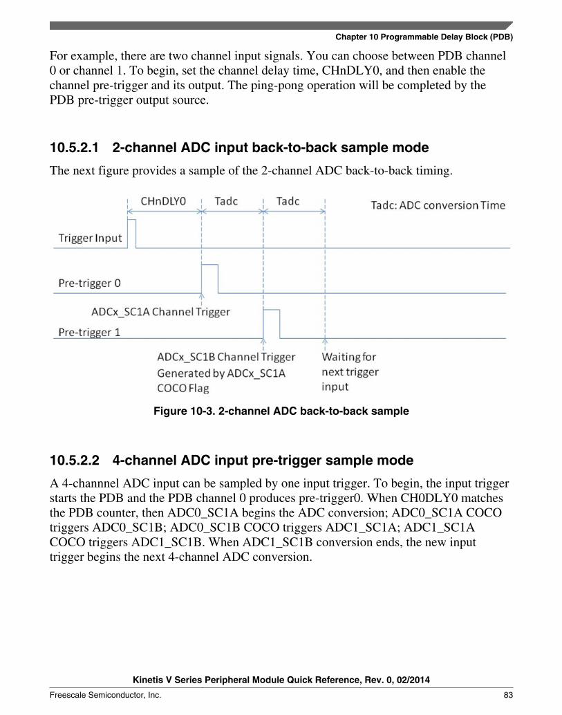
For example, there are two channel input signals. You can choose between PDB channel0 or channel 1. To begin, set the channel delay time, CHnDLY0, and then enable thechannel pre-trigger and its output. The ping-pong operation will be completed by thePDB pre-trigger output source.
10.5.2.1 2-channel ADC input back-to-back sample mode
The next figure provides a sample of the 2-channel ADC back-to-back timing.
Figure 10-3. 2-channel ADC back-to-back sample
10.5.2.2 4-channel ADC input pre-trigger sample mode
A 4-channnel ADC input can be sampled by one input trigger. To begin, the input triggerstarts the PDB and the PDB channel 0 produces pre-trigger0. When CH0DLY0 matchesthe PDB counter, then ADC0_SC1A begins the ADC conversion; ADC0_SC1A COCOtriggers ADC0_SC1B; ADC0_SC1B COCO triggers ADC1_SC1A; ADC1_SC1ACOCO triggers ADC1_SC1B. When ADC1_SC1B conversion ends, the new inputtrigger begins the next 4-channel ADC conversion.
Chapter 10 Programmable Delay Block (PDB)
Kinetis V Series Peripheral Module Quick Reference, Rev. 0, 02/2014
Freescale Semiconductor, Inc. 83
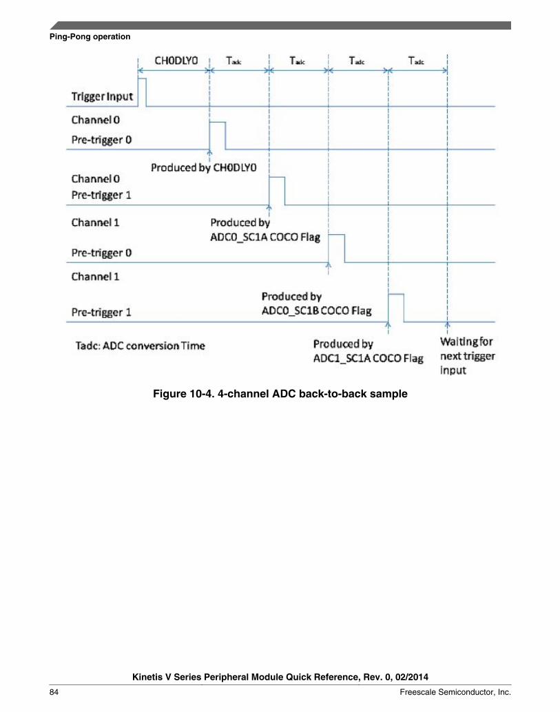
Figure 10-4. 4-channel ADC back-to-back sample
Ping-Pong operation
Kinetis V Series Peripheral Module Quick Reference, Rev. 0, 02/2014
84 Freescale Semiconductor, Inc.

Chapter 11Using FlexTimer (FTM) via Programmable DelayBlock (PDB) to Schedule ADC Conversion
11.1 OverviewThis chapter demonstrates how to use the PDB module to schedule and perform ADCconversions via FTM period trigger input, the ADCs works under 16-bit single-endmode, ADC0 samples the voltage on the ADC0_SE1(PTE16), and channelADC0_SE5(PTE17), and ADC1 samples the voltage ADC1_SE1(PTE18) andADC1_SE7(PTE18) on TWR-KV10Z32 board. And print the buffered 256 setconversion result via CDC virtual serial port of OpenSDA.
The code example shows how to:
• Make a low-level driver for the ADC, PDB and FTM• Show how to calibrate the ADC before ADC conversion• Configure the ADC for averaging a single-ended voltage conversion• Schedule ADC conversions with the PDB via FTM channel interrupt
11.2 IntroductionTiming of ADC conversions relative to system events is a key to applications, such asmotor control, and metering, requiring timing of ADC conversions for the best time to geta noise-reduced reading. When the Kinetis V MCU is acting as a controller, it will outputcontrol changes from time to time. Scheduling ADC conversions around these changes,which may make transient disturbances in the system, is key. Scheduling the ADCconversions at a time after the transient effects of the last control change has been madecan enable smooth operation of control loops. The PDB allows simple scheduling of oneor both of the ADC peripherals conversions. In this example, both ADC’s will bescheduled.
Kinetis V Series Peripheral Module Quick Reference, Rev. 0, 02/2014
Freescale Semiconductor, Inc. 85

11.3 FeaturesThe ADC features demonstrated by the PWM_PDB_ADC_Lab example code include:
• Simple calibration of the ADC:
A simple driver for the ADC, which facilitates using both ADCs and their calibrationwith minimal software, is included in the adc_demo example code. Prior to takingthe first measurement, during the initialization of the demo project the ADC will becalibrated. The use of the driver of the ADC will simplify this. While the ADC canbe used prior to calibration for conversions, the calibration of the ADC enables it tomeet its specifications.
• Averaging by 1, 4, 8, 16, or 32:
The ADC’s ability to average up to thirty-two conversion values prior to ending theconversion process and generating a result will be demonstrated. This feature reducesCPU load; it also reduces the effect of a noise spike on any readings. It is a simplearithmetic averaging of thirty-two (or less if so configured) ADC conversions. Theseconversions are taken upon the PDB triggering the ADC.
• The ADC’s interrupts:
The interrupt feature of the ADC is also used in the example. The ADC conversionresult is read from ADCx_Rn registers in the Interrupt Service of ADC0 and ADC1.
• Hardware triggering of the ADC with the FTM via PDB:
The ADC works with the FTM to trigger the ADC’s conversions. Determining whichADC trigger to convert is based on your configuration choices. In this case the ADCwill be configured to be triggered only by the FTM channel flag via PDB. The pre-trigger works under back-to-back mode.
• 16-bit resolution:
The conversion results in this example are 16 bit unsigned.
• Differential or single-ended:
Single-ended mode is illustrated in this example.
Features
Kinetis V Series Peripheral Module Quick Reference, Rev. 0, 02/2014
86 Freescale Semiconductor, Inc.

11.4 Configuration codeIn this case the ADCs are configured with four channels in ping-pong fashion trigged bythe back-to-back mode of the PDB. The input trigger source is from the periodic FTMchannel flag. ADC inputs are not connected to anything of interest for this demo.ADC0_SE1(PTE16) pin is written to ADC0_SC1A[ADCH] and channelADC0_SE5(PTE17) pin is written to ADC0_SC1B[ADCH]. ADC1_SE1(PTE18) pin isfilled in ADC1_SC1A[ADCH] and ADC1_SE7(PTE19) pin is filled inADC1_SC1B[ADCH].
11.4.1 FTM trigger 4-channel ADC ping-pong conversion viaback-to-back mode of PDB
There are several steps taken in the course of the execution of this demo, involvingsetting up the peripherals. These steps are further detailed with code from thePWM_PDB_ADC_Lab project and explained in the sections that follow, numbered afterthe manner of the steps:
1. ADC calibration.2. ADC initialization. Configure ADC clock source and set ADC clock to 18.75MHz,
select ADC 12-bit single mode, enable ADC interrupt, and setup ADC ISR. Write 4channel ADC external input to ADC0 and ADC1.
3. Configure PDB module, configure PDB trigger source and write pre-trigger delaytime. PDB works under back-to-back mode, only channel 0 pre-trigger0 is producedby CH0DLY0 register. The rest pre-triggers are produced by ADC conversionCOCO flag.
4. Configure the FTM, set FTM0 Combine mode, and set duty cycle, dead time. EnableFTM clock. Select FTM0 Channel 0 flag as FTM0 trigger source, then enable FTMclock source and start FTM.
5. When FTM0 channel0 flag is set, it is PDB input trigger, and PDB start to run, whenPDB channel 0 pre-trigger0 is set, it trigger ADC conversion, the COCO flag triggerADC0_SC1B, ADC1_SC1A and ADC1_SC1B conversion one by one.
6. When the 4-channel ADC conversion ends, the ADC will be triggered by next inputtrigger of FTM0.
7. The ADC conversion result is read in ADC ISR, if 256 set ADC conversion result isavailable, MCU will send them via serial port.
Chapter 11 Using FlexTimer (FTM) via Programmable Delay Block (PDB) to Schedule ADC Conversion
Kinetis V Series Peripheral Module Quick Reference, Rev. 0, 02/2014
Freescale Semiconductor, Inc. 87

11.4.2 ADC configuration
The code provided here enables ADC configuration.
SIM->CLKDIV1 |= SIM_CLKDIV1_OUTDIV5EN_MASK | SIM_CLKDIV1_OUTDIV5(0x03); /*!<out5 divider is 4, clock source is 75/4MHz*/ pADC_Config->bClocklSelect = 0x02; /*!<clock source is alternative clock*/ pADC_Config->bConversionMode = 0x01; /*!<12-bit single-end mode*/ pADC_Config->bHardwareTriggerEn = TRUE; /*!<enble ADC hardware trigger*/ pADC_Config->bIntEn = TRUE; /*!<ADC0 and ADC1 interrupt enable*/ ADC_Cal(ADC0); /*!<ADC0 calibration*/ ADC_Cal(ADC1); /*!<ADC0 calibration*/ ADC_Init(ADC0, pADC_Config); /*!<inital ADC0*/ ADC_Init(ADC1, pADC_Config); /*!<inital ADC1*/ ADC_SetCallBack(0, ADC0_Task); ADC_SetCallBack(1, ADC1_Task); /* write ADC0 channel and ADC1 channel */ ADC0->SC1[0] = (ADC0->SC1[0]&(~0x1F))|0x01; /*!<write ADC0 channel 1*/ ADC0->SC1[1] = (ADC0->SC1[1]&(~0x1F))|0x05; /*!<write ADC0 channel 5*/ ADC1->SC1[0] = (ADC1->SC1[0]&(~0x1F))|0x01; /*!<write ADC1 channel 1*/ ADC1->SC1[1] = (ADC1->SC1[1]&(~0x1F))|0x07; /*!<write ADC1 channel 7*/
11.4.3 PDB configuration
The following code shows how to configure the PDB.
/* PDB module configuration */ pPDB_Config->bPDBEn = TRUE; /*!<enable PDB*/ pPDB_Config->u16ModulusValue = 1500; /*!<set modulo value*/ pPDB_Config->u16InterruptDelay = 1500; /*!<set interrupt delay value, it is not necessary if disable interrupt*/ pPDB_Config->u16Ch0Delay0 = 200; /*!<set channel 0 pretrigger 0 delay time*/ pPDB_Config->u16Ch0Delay1 = 1000; /*!<set channel 0 pretrigger 1 delay time*/ pPDB_Config->u16Ch1Delay0 = 200; /*!<set channel 1 pretrigger 0 delay time*/ pPDB_Config->u16Ch1Delay1 = 1000; /*!<set channel 1 pretrigger 1 delay time*/ pPDB_Config->u8Ch0PretriggerEn = 0x03; /*!<enable channel 0 pretrigger */ pPDB_Config->u8Ch1PretriggerEn = 0x03; /*!<enable channel 1 pretrigger */ pPDB_Config->u8Ch0PretriggerOut = 0x03; /*!<enable channel 0 pretrigger output */ pPDB_Config->u8Ch1PretriggerOut = 0x03; /*!<enable channel 1 pretrigger output */ /*channel delay is not necessary back-to-back is enable, the pretrigger is produced by ADC conversion ack*/ pPDB_Config->u8Ch0Back2BackEn = 0x02; /*!<enable channel 0 back-to-back mode */ pPDB_Config->u8Ch1Back2BackEn = 0x02; /*!<enable channel 1 back-to-back mode */ pPDB_Config->bTriggerSource = 0x08; /*!<trigger source is from FTM0 */ PDB_Init(pPDB_Config); /*!<inital PDB module */
11.4.4 FTM configuration
The following code demonstrates how to configure the FTM.
/* FTM module configuration */ FTM_PinConfig(); /*!<FTM ouput pin configuration*/ FTM_PWMInit(FTM0, FTM_PWMMODE_COMBINE, FTM_PWM_LOWTRUEPULSE); /*!<inital FTM to combine
Configuration code
Kinetis V Series Peripheral Module Quick Reference, Rev. 0, 02/2014
88 Freescale Semiconductor, Inc.
mode*/ /* set MOD value */ FTM_SetModValue(FTM0, 4678); /*!<set FTM period is 16KHz, the modulo value is equal (75000/16)-1 */ FTM_PWMDeadtimeSet(FTM0, 2, 0x13);/*!<set channln and channel n-1 dead time, 1us*/ /* set clock source and start the counter */ FTM_ClockSet(FTM0, FTM_CLOCK_SYSTEMCLOCK, FTM_CLOCK_PS_DIV1); /* set the duty cycle, note: only fit for combine mode */ FTM_SetDutyCycleCombine(FTM0, FTM_CHANNEL_CHANNEL1, 50); FTM_SetDutyCycleCombine(FTM0, FTM_CHANNEL_CHANNEL3, 50); FTM_SetDutyCycleCombine(FTM0, FTM_CHANNEL_CHANNEL5, 50); FTM0->EXTTRIG = 0x10; /*!<trigger source is from FTM0 channel 0 trigger */ /* read ADC conversion u8Result */ while(u8CycleTimes<255); /*!< wait for u8Result0A[i],u8Result0B[i],u8Result1A[i] and u8Result1B[i] is full */ for(i=0;i<256;i++) /*!< print adc conversion result. */ { printf("%d, %d, %d, %d\n",u8Result0A[i],u8Result0B[i],u8Result1A[i],u8Result1B[i]); } printf("Please enter any character which will echo...\n"); /* echo chars received from terminal */ while(1) { u8Ch = UART_GetChar(TERM_PORT); UART_PutChar(TERM_PORT, u8Ch); } }
11.4.5 ADC ISR
The following code shows the ADC interrupt service routine which reads ADC resultsinto buffers.
/*****************************************************************************//*!** @brief ADC0 module task* * @param none ** @return none ** @ Pass/ Fail criteria: none*****************************************************************************/
void ADC0_Task(void){ if((ADC0->SC1[0] & ADC_SC1_COCO_MASK)==ADC_SC1_COCO_MASK) { u8Result0A[u8CycleTimes] = ADC0->R[0]; PTD->PTOR = (1<<7); } if((ADC0->SC1[1] & ADC_SC1_COCO_MASK)==ADC_SC1_COCO_MASK) { u8Result0B[u8CycleTimes] = ADC0->R[1]; PTD->PTOR = (1<<6);
} }
/*****************************************************************************//*!** @brief ADC1 module task*
Chapter 11 Using FlexTimer (FTM) via Programmable Delay Block (PDB) to Schedule ADC Conversion
Kinetis V Series Peripheral Module Quick Reference, Rev. 0, 02/2014
Freescale Semiconductor, Inc. 89

* @param none ** @return none ** @ Pass/ Fail criteria: none*****************************************************************************/
void ADC1_Task(void){ if((ADC1->SC1[0] & ADC_SC1_COCO_MASK)==ADC_SC1_COCO_MASK) { u8Result1A[u8CycleTimes] = ADC1->R[0]; } if((ADC1->SC1[1] & ADC_SC1_COCO_MASK)==ADC_SC1_COCO_MASK) { u8Result1B[u8CycleTimes] = ADC1->R[1]; u8CycleTimes++; } }
Configuration code
Kinetis V Series Peripheral Module Quick Reference, Rev. 0, 02/2014
90 Freescale Semiconductor, Inc.

Chapter 12FlexTimer Module (FTM)
12.1 OverviewThis chapter will demonstrate the features of the FlexTimer Module (FTM) of Kinetis Vseries devices. It also presents examples of how to properly configure the module toachieve its required operational mode. One of the examples included in this chapterutilizes two different modes of FTM operation: input capture and PWM mode. Anotherexample mentions the PWM functionality of FTM working in very low power stop mode(VLPS).
12.2 IntroductionThe FTM is built on the base of TPM module well known from Freescale 8-bitmicrocontrollers. The FTM extends the functionality to meet the demands of motorcontrol, digital lighting solutions, and power conversion, while providing low cost andbackwards compatibility with the TPM module.
12.3 FeaturesThe features of FTM on all Kinetis V series devices can vary in the number of FTMs andthe channels included in each module. The FTM functionality can be summarized into sixbasic modes of operation:
• Input capture• Output compare• PWM• Deadtime insertion• Quadrature decoder• Fault control
Kinetis V Series Peripheral Module Quick Reference, Rev. 0, 02/2014
Freescale Semiconductor, Inc. 91

The timer can also operate as a free running 16-bits counter.
12.3.1 FTM clock
The FTM source clock is selectable:
• System clock• Fixed frequency clock• External clock
Source clock can be the system clock, the fixed frequency clock, or an external clock.Fixed frequency clock is an additional clock input to allow the selection of an on-chipclock source other than the system clock. Selecting external clock connects FTM clock toa chip level input pin therefore allowing to synchronize the FTM counter with an off chipclock source.
The prescaler divide-by 1, 2, 4, 8, 16, 32, 64, or 128.
12.3.2 Interrupts and DMA
FTM supports three types of interrupt:
• Timer overflow interrupt• Channel (n) interrupt• Fault interrupt
The channel generates a DMA transfer request according to DMA and CHnIE bits.
12.3.3 Modes of operation
If no mode is selected by MSBx bits in channel status and control register, the counter isfully operational but there is no pin control. Therefore edge/level sensitivity selection byELSx bits does not play any role.
In an input capture mode, rising, falling, or both edges can be captured. Consideringsome restrictions, it allows this module to measure, for example, pulse width or timeperiod of input signal. Captured edge values can be read from FTMx_CnV. Any writes tothis register are ignored in input capture mode. For some selected FTM channels,comparator output can also be used for capturing.
Features
Kinetis V Series Peripheral Module Quick Reference, Rev. 0, 02/2014
92 Freescale Semiconductor, Inc.

In an output compare mode, set, clear, or toggle of output on match can be achieved. Thismode also allows the generation of positive or negative pulses on the match event. Thisevent occurs on compare match of FTMx_CNT and FTMx_CnV.
The most useful feature of the FTM is pulse width modulation (PWM). Edge- (upcounting) and center- (up-down counting) aligned PWM are available in this timermodule via FTMx_SC[CPWMS]. Both modes of operation provide positive (high true) ornegative (low true) PWM pulse generation. The channel pulse width is a proportional partof modulo value and is defined by FTMx_CnV. Combine mode is not available in thismodule.
12.3.4 Updating MOD and CnV
Any writes to FTMx_MOD or FTMx_CnV latch the value into an equivalent registerbuffer. The register is updated by its buffer value depending on clock mode selection:
• When the FTM is disabled by CMOD then MOD or CnV registers are updatedimmediately after they are written.
• When the FTM is enabled by CMOD and selected mode is output compare the CnVregister is updated on the next counter increment immediately after CnV register waswritten.
• In every other case the MOD and CnV registers are updated immediately after theFTM counter reaches the MOD value.
12.3.5 FTM period
The FTM time period is based on the period of the FTM source clock, prescaler value,modulo value, and also depends on alignment in the case of PWM mode. Therefore, theperiod of FTM can be calculated as:
Equation 1. FTM period calculation
For example, when:
• The system clock = 48 MHz is selected as a source clock for counter. The CLKS[1:0]bits in the SC register are 01
• Prescaler factor is selected to divide source clock by 16 (FTMx_SC_PS = 0x4)• The FTM modulo value is set to 3000 (FTMx_MOD = 0x0BB8) and edge aligned
mode is selected
Chapter 12 FlexTimer Module (FTM)
Kinetis V Series Peripheral Module Quick Reference, Rev. 0, 02/2014
Freescale Semiconductor, Inc. 93

Equation 2. FTM period calculation example
12.3.6 Additional features
The global time base feature can be used for the synchronization of all modules. In thiscase, all modules use the same time base. Only one FlexTimer module is used as globaltime, as detailed in the device reference manual.
FTM continues to function in debug mode. The behavior of FTM in debug mode isconfigured by FTMx_CONF.BDMMODE[1:0].
12.4 Configuration examplesTwo basic examples of FTM configuration will be demonstrated in this section. The firstexample uses edge-aligned PWM and the second example shows input capture features ofFTM working in normal run mode.
NOTEIn these examples, TWR-KV10Z32 with PKV10Z32 is used.Optionally, TWR-PROTO, TWR-ELEV, and TWR-SER can beused.
12.4.1 Example – Edge Aligned PWM and Input Capture Mode
This example demonstrates the basic features of the FTM, such as input capture andedge-aligned PWM mode. In this case, FTM0 is configured to work in edge-alignedPWM mode. This module uses two channels: channel 1 and channel 2.
Channel 1 is configured to generate positive PWM pulses. Channel 2 is configured togenerate negative PWM pulses (inverse PWM). Module FTM1 is configured to work ininput capture mode. Channel 0 is configured to capture rising edges and in contrastchannel 1 is configured to capture falling edges. The purpose of this configuration is to beable to measure, for example, the pulse width of the pulses generated by FTM0. This canbe achieved by interconnecting channel 1 of FTM0 and both channels of FTM1, asshown in the following figure.
Configuration examples
Kinetis V Series Peripheral Module Quick Reference, Rev. 0, 02/2014
94 Freescale Semiconductor, Inc.

Edge Aligned PWM
CH2Negative pulses
FTM0
CH1Positive pulses
Input Capture Mode
CH1Falling edge
FTM1
CH0Rising edge
out
out
in
in
Figure 12-1. Interconnection of FTM modules in example
Before configuring both FTM modules, SIM must configure all required clock options. Inthis example, system clock is used as a source clock for FTM. Therefore, it is necessaryto set FTMx_SC.CLKS[1:0] to 1. Next, the clocks for the ports whose pins will be usedmust also be enabled. In this example, pin PTC2 and PTC3 are used as channel outputs ofFTM0, and PTD6 and PTD7 are used as channel inputs of FTM1. Therefore, clocks forPORTC must be enabled. In the end, the clock gates must be enabled for both of theFTMs used. Follow the next few lines of code with required SIM module configuration.
/* Enable PORTC/D clocks */ SIM->SCGC5 |= SIM_SCGC5_PORTC_MASK | (SIM_SCGC5_PORTD_MASK; /* Enable FTM0/1 clocks */ SIM->SCGC6 |= SIM_SCGC6_FTM0_MASK; SIM->SCGC6 |= SIM_SCGC6_FTM1_MASK;
NOTEIf any additional clock settings are required in your application,they must also be implemented in SIM configuration.
After SIM initialization, required port pins must be configured according to their use. It isnecessary to clear only interrupt status flag, select an alternative pin for the FTM channel,and for outputs you can enable drive strength.
/* Enable the FTM0 Ch1/2 function on PTC2/3 */ PORTC->PCR[2] = PORT_PCR_MUX(0x4); PORTC->PCR[3] = PORT_PCR_MUX(0x4); /* Enable the FTM1 Ch0/1 function on PTD6/7*/ PORTD->PCR[6] = PORT_PCR_MUX(0x5); PORTD->PCR[7] = PORT_PCR_MUX(0x5);
The next step is the configuration of FlexTime modules. FTM0 configuration isdemonstrated first. In this module, timer overflow interrupt will be enabled. Therefore,NVIC must be set before module interrupt is enabled.
/* enable FTM2 interrupt in NVIC */ NVIC_EnableIRQ(FTM0_IRQn);
You can also redefine interrupt vector to your interrupt service routine. This must bedone in a different module, such as isr.h.
extern void FTM0_Isr(void);
#undef VECTOR_033#define VECTOR_033 FTM0_Isr
Chapter 12 FlexTimer Module (FTM)
Kinetis V Series Peripheral Module Quick Reference, Rev. 0, 02/2014
Freescale Semiconductor, Inc. 95
Then FTM0 module can be initialized. FTM0_CONF should stay in its default state. Forbest performance, initialize the counter, that is, write to FTM0_CNT, before writing tothe modulo register. Modulo value MOD is set to 4800 to generate a PWM signal with10 kHz,assuming that the system clock is set to 48 MHz. Then FTM0_SC will enabletimer overflow interrupt, set edge-aligned (up counting) mode, select clock mode to allowthe counter to increment on every clock, and set the prescaler divider to 1.
/* update MOD value */FTM_SetModValue(FTM0, 4800); /* set clock source, start counter */FTM_ClockSet(FTM0, FTM_CLOCK_SYSTEMCLOCK, FTM_CLOCK_PS_DIV1);
Channels configuration must be done after general FTM0 module configuration. Channel1 of FTM0 is configured as edge-aligned PWM with high-true pulses (positive PWMpulses). Channel 2 is configured as edge-aligned PWM with low-true pulses (negativepulses). Channel interrupt is disabled. Channels value must also be initialized.
pFTM->CONTROLS[1].CnSC = FTM_CnSC_MSB_MASK | FTM_CnSC_ELSB_MASK; pFTM->CONTROLS[1].CnV = 0; pFTM->CONTROLS[2].CnSC = FTM_CnSC_MSB_MASK | FTM_CnSC_ELSA_MASK; pFTM->CONTROLS[2].CnV = 0;
NOTEBoth channels of the FTM are configured in inverse PWM todemonstrate how one leg of the three phase converter used inmotor control application can be configured. Also note thatdead time control is available in the Kinetis V series FTM.
This module generates interrupt on timer overflow. It is convenient to clear thecorresponding flag in interrupt service routine. Value register is also set.
void FTM0_Isr(void){ /* clear the flag */ FTM_ClrOverFlowFlag(FTM0);
/* update the channel value */ FTM_SetChannelValue(FTM0, FTM_CHANNEL_CHANNEL1, u16ChV_new);}
NOTESetting the compare value in the timer overflow interruptservice routine of the same FTM is not a best practice. CnVregisters are updated by their buffer value immediately aftertimer overflow. Therefore, one period of FTM can be lost insuch a case. Instead, set compare value immediately beforetimer overflow.
Configuration examples
Kinetis V Series Peripheral Module Quick Reference, Rev. 0, 02/2014
96 Freescale Semiconductor, Inc.

After FTM0 initialization, FTM1 should be initialized. As mentioned previously, thismodule is configured to work in input capture mode. This module is also configured togenerate interrupt on timer overflow. It is then required to enable vector interrupt for thismodule and set priority as in previous FTM configuration.
NVIC_EnableIRQ(FTM1_IRQn);
In isr.h, redefine interrupt vector.
extern void FTM1_Isr(void);
#undef VECTOR_034#define VECTOR_034 FTM1_Isr
Because pulse width measurement uses FTM1, it is desirable to trigger start of FTM1counting by FTP0 overflow. Therefore, FTM0_CONF sets input trigger to TMP0overflow and enables counter start on trigger. For more information, see Figure 13-2.Counter is set to stop on overflow and input trigger provides its restart. The rest of theconfiguration is similar to FTM0, except modulo value, which can be set higher. In thisexample, it was set to 11200, assuming FTM1 period is 4285 Hz.
FTM_ClockSet(FTM1, FTM_CLOCK_SYSTEMCLOCK, FTM_CLOCK_PS_DIV1);FTM_EnableChannelInt(FTM1, 1);
Channels of FTM1 are configured to input capture mode. Channel 0 is configured tocapture rising edges and channel 1 is configured to capture falling edges. There is nointerrupt on the generated channel event.
/* configure FTM1_CH0 and FTM1_CH1 to measure the input wave pulse width */FTM_DualEdgeCaptureInit( FTM1, FTM_CHANNELPAIR0,FTM_INPUTCAPTURE_DUALEDGE_ONESHOT,FTM_INPUTCAPTURE_DUALEDGE_RISINGEDGE,FTM_INPUTCAPTURE_DUALEDGE_FALLInGEDGE );
FTM1 also generates interrupt on time overflow. In the interrupt service routine, thetimer overflow flag is cleared and pulse width is calculated from the rising and fallingedges values of channels. Channel flags must also be cleared in to be able to captureedges in the next FTM1 period.
void FTM1_Isr(void){ FTM_ClrChannelFlag(FTM0, FTM_CHANNELPAIR0); FTM_ClrChannelFlag(FTM0, FTM_CHANNELPAIR0+1); u8IntMark = 1;}
NOTEWhen a different input signal will supply FTM1 inputs, then itis recommended to increase modulo value to 65535 to reach thehighest possible resolution of pulse width measurement. Alsonote that if the result of pulse width is negative, it should not betaken into account. In this case, rising edge (FTM1_C0V) wascaptured two periods before and falling edge (FTM1_C1V) was
Chapter 12 FlexTimer Module (FTM)
Kinetis V Series Peripheral Module Quick Reference, Rev. 0, 02/2014
Freescale Semiconductor, Inc. 97
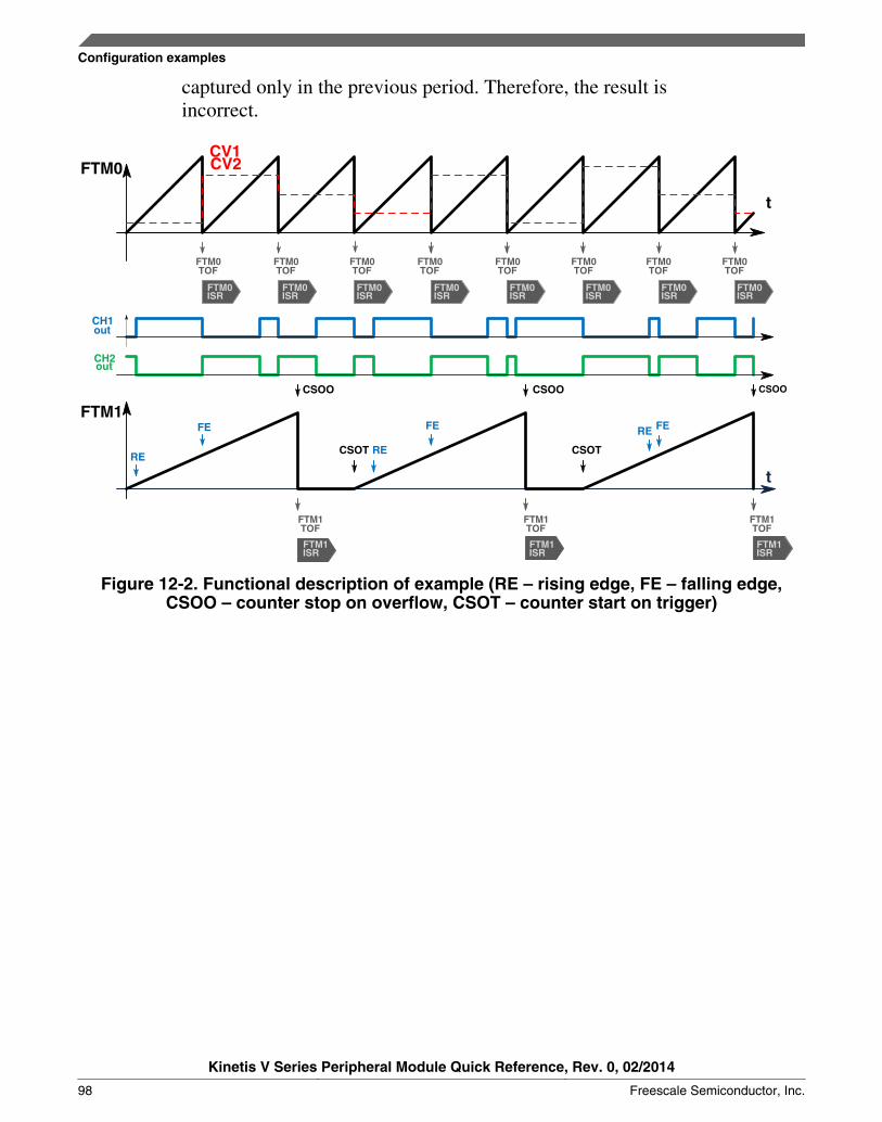
captured only in the previous period. Therefore, the result isincorrect.
PM0
CSOO
CV2CV1
FTM0
t
t
CH1 out
FTM1
CH2 out
CSOO
CSOT
CSOO
RE
FE
RE
FE RE FE
FTM1 TOF
FTM0 ISR
CSOT
FTM1TOF
FTM1TOF
FTM0TOF
FTM0TOF
FTM0TOF
FTM0TOF
FTM0TOF
FTM0ISR
FTM0ISR
FTM0ISR
FTM0ISR
FTM0ISR
FTM0ISR
FTM0ISR
FTM0TOF
FTM0TOF
FTM0TOF
FTM1ISR
FTM1ISR
FTM1ISR
Figure 12-2. Functional description of example (RE – rising edge, FE – falling edge,CSOO – counter stop on overflow, CSOT – counter start on trigger)
Configuration examples
Kinetis V Series Peripheral Module Quick Reference, Rev. 0, 02/2014
98 Freescale Semiconductor, Inc.

Appendix AHow to Load QRUG Examples
A.1 OverviewThis chapter describes how to load and run the sample code described in other sections ofthe Kinetis V series Quick Reference User Guide. It describes the procedures used toensure your Tower system or Freedom board is connected properly, and explains how toload the example projects.
A.2 Software configurationFor compiling, flash downloading, and debug functioning, you will need to install IARSystem's Embedded Workbench for ARM (EWARM) V6.70.3 or later, as well as anypatches and updates available at www.iar.com. EWARM supports Open SDA, thefirmware located on your Kinetis V series Tower board that enables you to flash anddebug code with only a mini-B USB cable.
The projects you will be working with can be found on the Freescale website:www.freescale.com
Using the EWARM and installing and downloading the project files to the Kinetis Vseries Tower board will enable you to use the OPEN SDA interface.
A.3 Hardware configurationThe examples can be run with the Kinetis V series microcontroller module in stand-alonemode. Alternatively, you can put together your Tower kit for examples using serial achannel interface without using the Open SDA serial channel.
Connect a USB cable to the mini-USB port on the Kinetis V series board. This will be:
• J23 on TWR_KV10Z32
Kinetis V Series Peripheral Module Quick Reference, Rev. 0, 02/2014
Freescale Semiconductor, Inc. 99

When you plug in the USB cable to your board, you will see LEDs on the board turn on.
A.4 Terminal configurationThe OPEN SDA feature on the Kinetis V series Tower board will create a serial port thatcommunicates to your computer over the USB cable, which was connected in theprevious section. This virtual serial port is connected to UART0 on the TWR-KV10Z.
To configure the terminal:
1. Open your computers device manager and look in the COM Ports and read whatCOM port number is assigned to the OPEN SDA port.
2. Open the Terminal Utility.3. Configure the terminal client to use indicated COM port, 115200 baud, 8 data bits, 1
stop bit, and no parity.4. Then open the Serial Port to start the connection.
A.5 Download sample codeTo download sample code:
1. Save locally the latest sample code for your Tower module from:• http://www.freescale.com/webapp/sps/site/prod_summary.jsp?code=TWR-
KV10Z322. Run the install and save into any directory.3. Go to kvxx-drv-lib\build\iar\ to see all of the different projects available.4. The next section describes running the basic low power demo example, but the same
instructions can also be used with other projects.
A.6 Running the "Blinky_green" projectTo run this project:
1. Open IAR and go to File -> Open -> Workspace in the menu bar.2. Open the Blinky_green workspace at kvxx-drv-lib\build\iar\kv10\Blinky_green\.3. The workspace that opens contains a “Blink_green” project for the TWR-KV10Z.4. There are two flash combinations available in the demo which this project supports;
FLASH_32KB and FLASH_16KB. Select FLASH_32KB for the TWR_KV10board.
Terminal configuration
Kinetis V Series Peripheral Module Quick Reference, Rev. 0, 02/2014
100 Freescale Semiconductor, Inc.
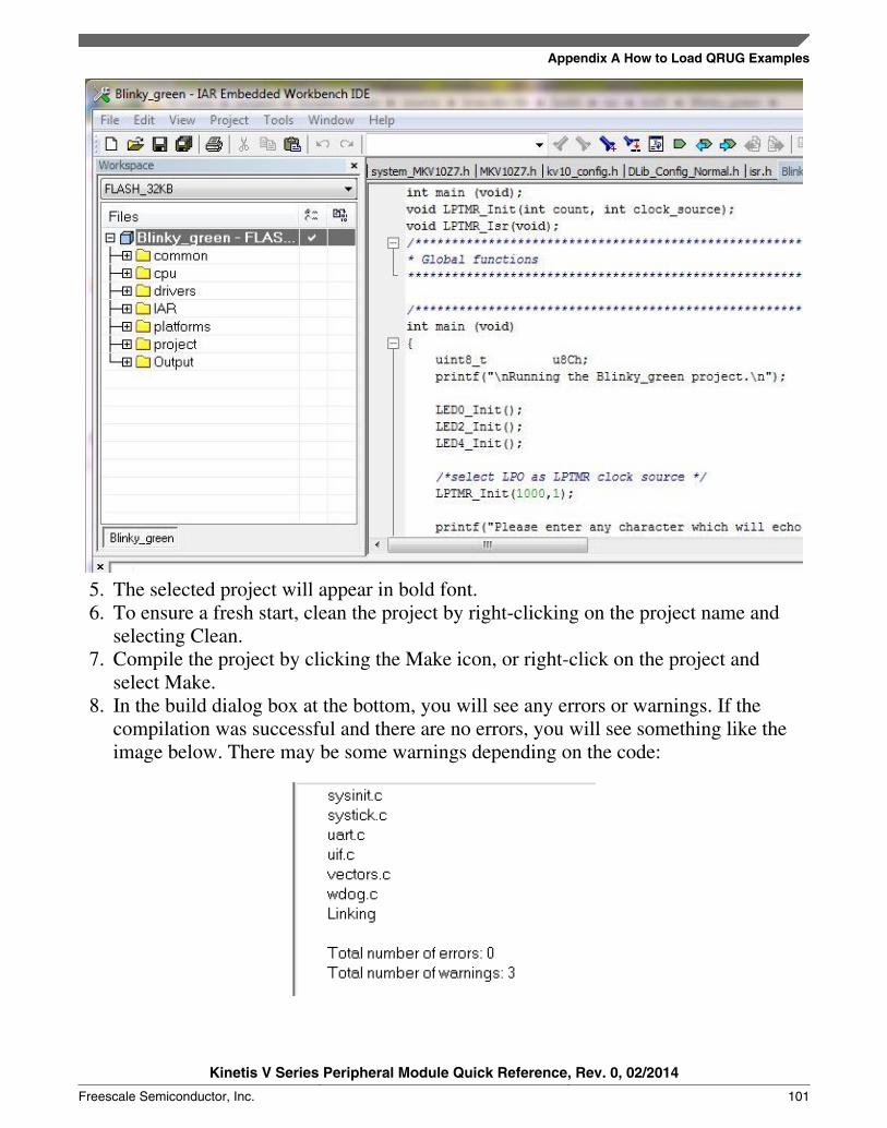
5. The selected project will appear in bold font.6. To ensure a fresh start, clean the project by right-clicking on the project name and
selecting Clean.7. Compile the project by clicking the Make icon, or right-click on the project and
select Make.8. In the build dialog box at the bottom, you will see any errors or warnings. If the
compilation was successful and there are no errors, you will see something like theimage below. There may be some warnings depending on the code:
Appendix A How to Load QRUG Examples
Kinetis V Series Peripheral Module Quick Reference, Rev. 0, 02/2014
Freescale Semiconductor, Inc. 101

9. Download the code to the board and start the debugger by pressing the Downloadand Debug button.
10. The code will download into flash. The debugger screen will appear and pause at thefirst instruction. Click the Go button to start running.
11. After you select Go, the software will print out information and indicate to input anycharacter which will echo, meanwhile the green LED (D1,D3,D5) begins to blink.
Running the Blinky_green project.Please enter any character which will echo...
Kinetis V Series Peripheral Module Quick Reference, Rev. 0, 02/2014
102 Freescale Semiconductor, Inc.

How to Reach Us:
Home Page:freescale.com
Web Support:freescale.com/support
Information in this document is provided solely to enable system andsoftware implementers to use Freescale products. There are no expressor implied copyright licenses granted hereunder to design or fabricateany integrated circuits based on the information in this document.Freescale reserves the right to make changes without further notice toany products herein.
Freescale makes no warranty, representation, or guarantee regardingthe suitability of its products for any particular purpose, nor doesFreescale assume any liability arising out of the application or use ofany product or circuit, and specifically disclaims any and all liability,including without limitation consequential or incidental damages.“Typical” parameters that may be provided in Freescale data sheetsand/or specifications can and do vary in different applications, andactual performance may vary over time. All operating parameters,including “typicals,” must be validated for each customer application bycustomer's technical experts. Freescale does not convey any licenseunder its patent rights nor the rights of others. Freescale sells productspursuant to standard terms and conditions of sale, which can be foundat the following address: freescale.com/SalesTermsandConditions.
Freescale, the Freescale logo, and Kinetis are trademarks of FreescaleSemiconductor, Inc., Reg. U.S. Pat. & Tm. Off. Tower is a trademark ofFreescale Semiconductor, Inc. ARM, ARM Powered, and Cortex areregistered trademarks of ARM Limited (or its subsidiaries) in the EUand/or elsewhere. All rights reserved. All other product or service namesare the property of their respective owners.
© 2014 Freescale Semiconductor, Inc. All rights reserved.
Document Number KVQRUGRevision 0, 02/2014


