ZiLOG Worldwide Headquarters • 532 Race Street • San Jose, CA 95126-3432 Telephone: 408.558.8500 • Fax: 408.558.8300 • http://www.ZiLOG.com Product Specification PS011802-0902 Z84C90 KIO Serial/Parallel Counter Timer
Transcript
ZiLOG Worldwide HTelephone: 408
Z84C90
KIO Serial/Parallel Counter Timer
Product Specification
PS011802-0902
eadquarters • 532 Race Street • San Jose, CA 95126-3432.558.8500 • Fax: 408.558.8300 • http://www.ZiLOG.com
PS011802-0902
This publication is subject to replacement by a later edition. To determine whether a later edition exists, or to request copies of publications, contact:
ZiLOG Worldwide Headquarters532 Race StreetSan Jose, CA 95126-3432Telephone: 408.558.8500Fax: 408.558.8300www.ZiLOG.com
Windows is a registered trademark of Microsoft Corporation.
KIO Serial/Parallel Counter/TimerProduct Specification
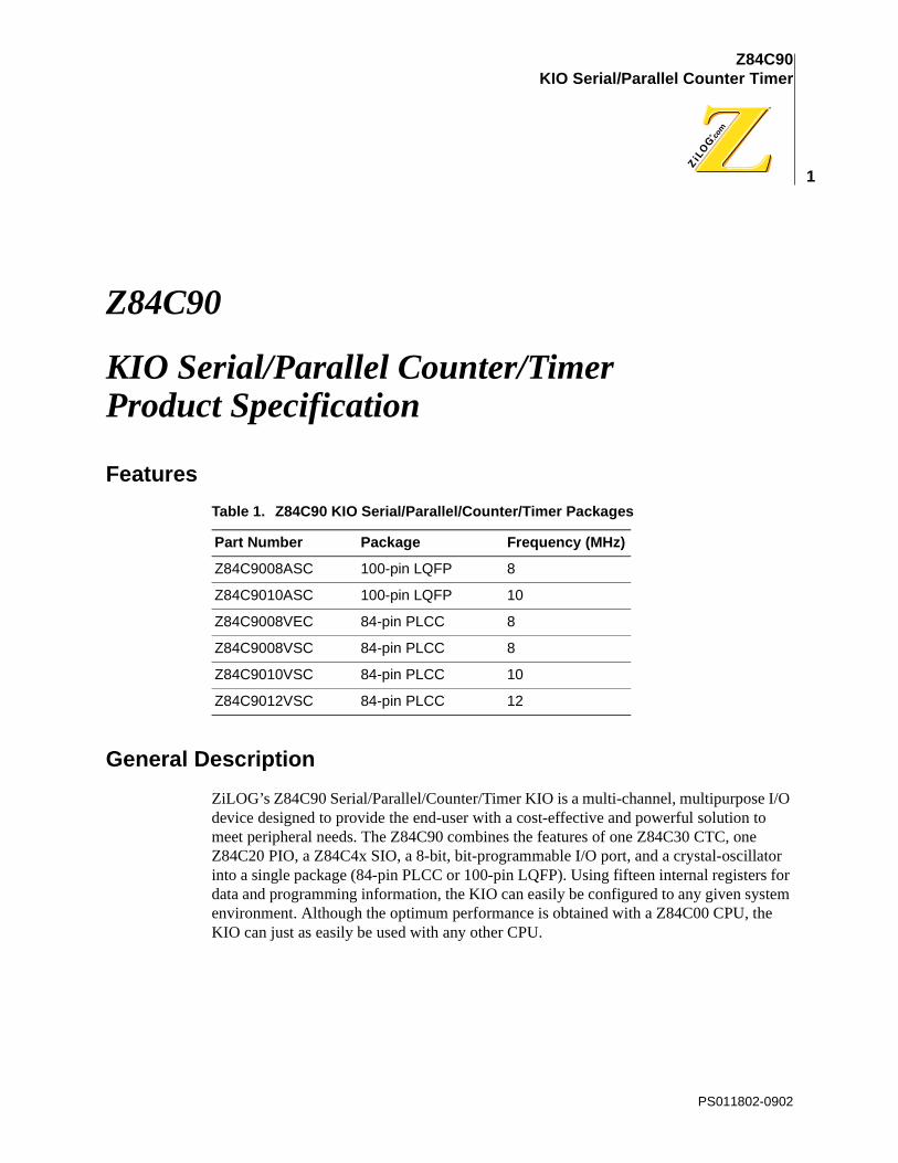
Features
General DescriptionZiLOG’s Z84C90 Serial/Parallel/Counter/Timer KIO is a multi-channel, multipurpose I/O device designed to provide the end-user with a cost-effective and powerful solution to meet peripheral needs. The Z84C90 combines the features of one Z84C30 CTC, one Z84C20 PIO, a Z84C4x SIO, a 8-bit, bit-programmable I/O port, and a crystal-oscillator into a single package (84-pin PLCC or 100-pin LQFP). Using fifteen internal registers for data and programming information, the KIO can easily be configured to any given system environment. Although the optimum performance is obtained with a Z84C00 CPU, the KIO can just as easily be used with any other CPU.
Table 1. Z84C90 KIO Serial/Parallel/Counter/Timer Packages
Part Number Package Frequency (MHz)
Z84C9008ASC 100-pin LQFP 8
Z84C9010ASC 100-pin LQFP 10
Z84C9008VEC 84-pin PLCC 8
Z84C9008VSC 84-pin PLCC 8
Z84C9010VSC 84-pin PLCC 10
Z84C9012VSC 84-pin PLCC 12
PS011802-0902
Z84C90KIO Serial/Parallel Counter Timer
2
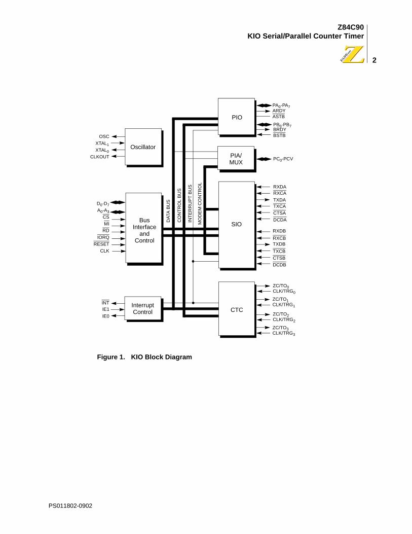
Figure 1. KIO Block Diagram
Oscillator
BusInterface
andControl
InterruptControl
PIO
PIA/MUX
SIO
CTC
OSCXTAL1XTAL0
CLKOUT
D0-D7A0-A3
CSMI
RDIORQ
RESETCLK
INTIE1IE0
PA0-PA7ARDYASTB
PB0-PB7BRDYBSTB
PC0-PCV
RXDARXCATXDATXCACTSADCDA
RXDBRXCBTXDBTXCBCTSBDCDB
ZC/TO0CLK/TRG0
ZC/TO1CLK/TRG1
ZC/TO2CLK/TRG2
ZC/TO3CLK/TRG3
DAT
A BU
S
CO
NTR
OL
BUS
INTE
RR
UPT
BU
S
MO
DEM
CO
NTR
OL
PS011802-0902
Z84C90KIO Serial/Parallel Counter Timer
3
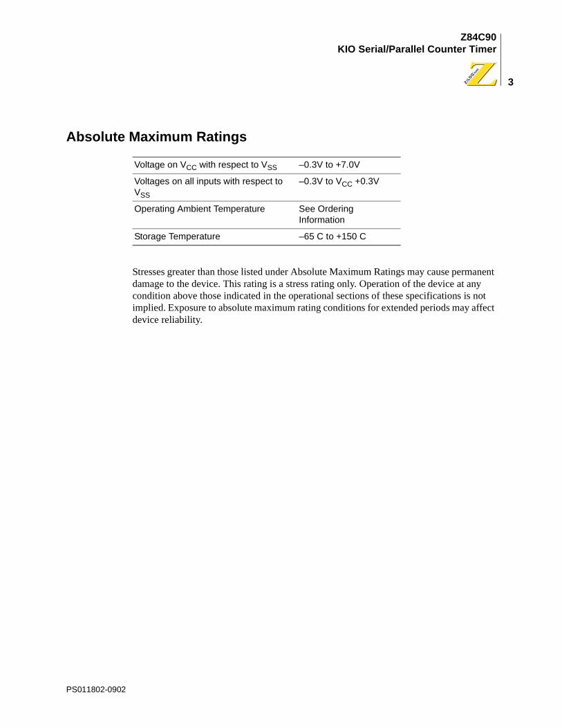
Absolute Maximum Ratings
Stresses greater than those listed under Absolute Maximum Ratings may cause permanent damage to the device. This rating is a stress rating only. Operation of the device at any condition above those indicated in the operational sections of these specifications is not implied. Exposure to absolute maximum rating conditions for extended periods may affect device reliability.
Voltage on VCC with respect to VSS –0.3V to +7.0V
Voltages on all inputs with respect to VSS
–0.3V to VCC +0.3V
Operating Ambient Temperature See Ordering Information
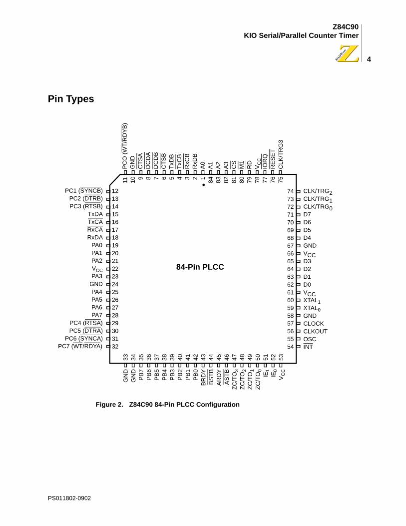
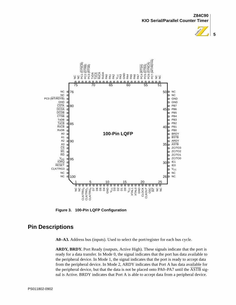
A0–A3. Address bus (inputs). Used to select the port/register for each bus cycle.
ARDY, BRDY. Port Ready (outputs, Active High). These signals indicate that the port is ready for a data transfer. In Mode 0, the signal indicates that the port has data available to the peripheral device. In Mode 1, the signal indicates that the port is ready to accept data from the peripheral device. In Mode 2, ARDY indicates that Port A has data available for the peripheral device, but that the data is not be placed onto PA0–PA7 until the ASTB sig-nal is Active. BRDY indicates that Port A is able to accept data from a peripheral device.
Port B does not support Mode 2 operation and can only be used in Mode 3 when Port A is programmed for Mode 2. BRDY is not associated with Port B when it is operating in Mode 3.
ASTB, BSTB. Port Strobe (inputs, Active Low). These signals indicate that the peripheral device has performed a transfer. In Mode 0, the signal indicates that the peripheral device has accepted the data present on the port pins. In Mode 1, the signal causes the data on the port pins to be latched onto Port A. In Mode 2, ASTB Low causes the data in the output data latch of Port A to be placed onto the Port A pins. BSTB Low causes the data present on the Port A pins to be latched into the Port A input data latch. The end of the current transaction is noted by the rising edge of these signals.
Port B does not support Mode 2 operation, and can only be used in Mode 3 when Port A is programmed for Mode 2. BSTB is not associated with Port B when it is operating in Mode 3.
CLK/TRG0–CLK/TRG3. External Clock/Timer Trigger (inputs, user-selectable Active High or Low). These four pins correspond to the four counter/timer channels of the KIO. In Counter mode, each active edge causes the downcounter to decrement. In Timer mode, an active edge starts the timer.
CLKOUT. Clock Out (output). This output is a divide-by-two of the oscillator (XTAL) input.
CLOCK. System Clock (input). This clock must be the same as (or a derivative of) the CPU clock. If the CLKOUT is to be used as the system clock, then these two pins must be connected together.
CS. Chip Select (input, Active Low). Used to activate the internal register decoding mech-anism and allow the KIO to perform a data transfer to/from the CPU.
CTSA, CTSB. Clear to Send (inputs, Active Low). These signals are modem control sig-nals for the serial channels. When programmed for Auto Enable, a Low on these pins enables their respective transmitters. If not programmed as Auto Enable, these pins may be used as general-purpose input signals.
D0–D7. Data Bus (bidirectional, Active High, 3-stated). Used for data exchanges between the CPU and the KIO for programming and data transfer. The KIO also monitors the data bus for RETI instructions to maintain its Interrupt Under Service (IUS) status.
DCDA, DCDB. Data Carrier Detect (inputs, Active Low). These signals are modem con-trol signals for the serial channels. When programmed for Auto Enable, a Low on these pins enables their respective receivers. If not programmed as Auto Enable, these pins may be used as general-purpose input signals.
DTRA, DTRB. Data Terminal Ready (outputs, Active Low). These signals are modem control signals for the serial channels. They follow the state programmed into their respec-tive serial channels, and are multiplexed with Port C, bits 5 and 2, respectively.
Note:
Note:
PS011802-0902
Z84C90KIO Serial/Parallel Counter Timer
7
IEI. Interrupt Enable In (input, Active High). This signal is used with Interrupt Enable Out (IEO) to form a priority daisy chain when there is more than one interrupt-driven device. A High on this line indicates that no higher-priority device is requesting an inter-rupt.
IEO. Interrupt Enable Out (output, Active High). This signal is used with Interrupt Enable In (IEI) to form a priority daisy chain when there is more than one interrupt-driven device. A High on this line indicates that this device is requesting an interrupt, and that no higher-priority device, is not requesting an interrupt. A Low blocks any lower-priority devices from requesting an interrupt.
IORQ. Input/Output Request (input, Active Low). IORQ is used with RD, A0–A3, and CS to transfer data between the KIO and the CPU. When IORQ, RD, and CS are Active Low, the device selected by A0–A3 transfers data to the CPU. When IORQ and CS are Active Low, but RD is Active High, the device selected by A0–A3 is written into by the CPU. When IORQ and M1 are both Active Low, the KIO may respond with an interrupt vector from its highest-priority interrupting device.
M1. Machine Cycle 1 (input, Active Low). When M1 and RD are Low, the Z80 CPU fetches an instruction from memory; the KIO decodes this cycle to determine if the RETI instruction sequence is being executed. When M1 and IORQ are both active, the KIO decodes the cycle to be an interrupt acknowledge, and may respond with a vector from its highest-priority interrupting device.
OSC. Oscillator (output). This output is a reference clock for the oscillator.
PA0–PA7. Port A Bus (bidirectional, tristated). One of the 8-bit ports of the PIO. PA0 is the least-significant bit of the bus.
PB0–PB7. Port B Bus (bidirectional, tristated). One of the 8-bit ports of the PIO. PB0 is the least-significant bit of the bus. This port can also supply 1.5mA at 1.5V to drive Dar-lington transistors.
PC0–PC7. Port C Bus (bidirectional, tristated). PC0 is the least-significant bit of the bus. These pins are multiplexed between the 8-bit PIA and additional modem control signals for the serial channels.
RD. Read (input, Active Low). When RD is active, a memory or I/O read operation is in progress. RD is used with A0–A3, CS and IORQ to transfer data between the KIO and CPU.
RESET. Reset (input, Active Low). A Low on this pin forces the KIO into a Reset condi-tion. This signal must be active for a minimum of three Clock cycles. The KIO resets so that the PIO ports operate in Mode 1
• With handshakes inactive and interrupts disabled
• PIA port in Input mode and active
• CTC channel counting terminated and interrupts disabled
PS011802-0902
Z84C90KIO Serial/Parallel Counter Timer
8
• SIO channels disabled
• Marking with interrupts disabled.
All control registers must be rewritten after a hardware reset.
RTSA, RTSB. Request to Send (outputs, Active Low). These signals are modem control signals for their serial channels. They follow the inverse state programmed into their respective serial channels, and are multiplexed with Port C, bits 4 and 3, respectively.
RxCA, RxCB. Receive Clock (inputs, Active Low). These clocks are used to assemble the data in the receiver shift register for their serial channels. Data is sampled on the rising edge of the clock.
RxDA, RxDB. Receive Data (inputs, Active High). These pins are the input data pins to the receive shift register for their serial channels.
SYNCA, SYNCB. Synchronization (bidirectional, Active Low). In the Asynchronous mode of operation, these pins act much like the CTS and DCD pins. Transitions affect the Sync/Hunt status bit for their respective serial channels, but serve no other purpose. These pins are multiplexed with Port C, bits 6 and 1, respectively.
TxCA, TxCB. Transmit Clock (inputs, Active Low). These clocks are used to transmit data from the transmit shift register for their serial channels. Data is transmitted on the falling edge of the clock.
TxDA, TxDB. Transmit Data (outputs, Active High). These pins are the output data pins from the transmitter for their serial channels.
WT/RDYA, WT/RDYB. Wait/Ready (outputs, open-drain when programmed as Wait; tristated when programmed as Ready). These pins may be programmed as Ready lines for a DMA controller or Wait lines for interfacing to a CPU. As a Ready line, these pins indi-cate (when Active Low) that the transmitter or the receiver requests a transfer between the serial channel and the DMA. As a Wait line, these pins dictate (when Low) that the CPU must wait until the transmitter or receiver can complete the requested transaction. These pins are multiplexed with Port C, bit 7 and 0, respectively.
XTALI. Crystal/Clock Connection. (input).
XTALO. Crystal Connection. (output).
ZC/TO0–ZC/TO3. Zero count/Time-out (outputs, Active High). These four pins are out-puts from the four counter/timer channels of the KIO. Each pin pulses High when its cor-responding downcounter reaches 0.
PS011802-0902
Z84C90KIO Serial/Parallel Counter Timer
9
Standard Test ConditionsThe DC Characteristics and Capacitance sections below apply to the following standard test conditions, unless otherwise noted. All voltages are referenced to GND (0V). Posi-tive current flows into the referenced pin.
Available operating temperature ranges are:
• S = 0° C to +70° C
• E = –40° C to +100° C
Voltage Supply Range: +5.0V ± 10%
All AC parameters assume a load capacitance of 100 pF. Add 10 ns delay for each 50 pF increase in load up to a maximum of 200 pF for the data bus and 100 pF for the address and control lines. AC timing measurements are referenced to 1.5 volts (except for CLOCK, which is referenced to the 10% and 90% points.
Table 2. KIO Registers
Address A3 A2 A1 A0
Register 0: PIO Port A Data 0 0 0 0
Register 1: PIO Port A Command 0 0 0 1
Register 2: PIO Port B Data 0 0 1 0
Register 3: PIO Port B Command 0 0 1 1
Register 4: CTC Channel 0 0 1 0 0
Register 5: CTC Channel 1 0 1 0 1
Register 6: 0 1 1 0
Register 7: 0 1 1 1
Register 8: SIO Port A Data 1 0 0 0
Register 9: SIO Port A Command/Status 1 0 0 1
Register 10: SIO Channel B Data 1 0 1 0
Register 11: SIO Channel B Command/Status 1 0 1 1
Register 12: PIA Port C Data 1 1 0 0
Register 13: PIA Port C Command 1 1 0 1
Register 14: KIO Command 1 1 1 0
Register 15: Reserved 1 1 1 1
Note: Additionally, IORQ and CS must be Low. Registers are written to or read from by the CPU, applying a 1 or a 0 respectively on the RD pin.
PS011802-0902
Z84C90KIO Serial/Parallel Counter Timer
10
The Ordering Information section lists temperature ranges and product numbers. Package drawings are in the Package Information section. Refer to the Literature List for additional documentation.
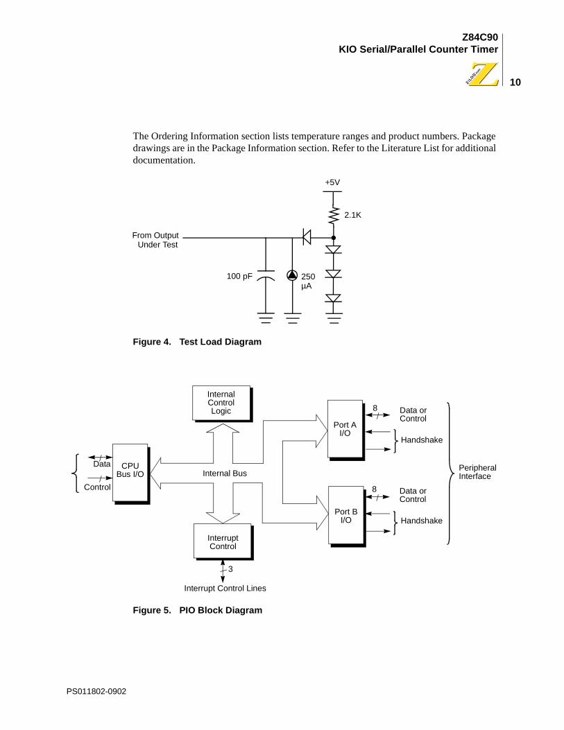
Figure 4. Test Load Diagram
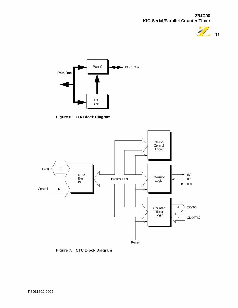
Figure 5. PIO Block Diagram
250
From OutputUnder Test
µA100 pF
+5V
2.1K
Data
Control
Data orControl
Handshake
Interrupt Control Lines
PeripheralInterface
InternalControlLogic
CPUBus I/O
Data orControl
Handshake
InterruptControl
Port AI/O
Port BI/O
Internal Bus
8
3
8
PS011802-0902
Z84C90KIO Serial/Parallel Counter Timer
11
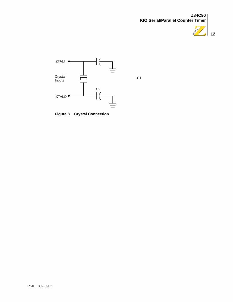
Figure 6. PIA Block Diagram
Figure 7. CTC Block Diagram
Port C
Dir.Ctrl.
Data BusPC0`PC7
Data
Control
INTIE1IE0
ZC/TO
CLK/TRG
Reset
Internal Bus
InternalControlLogic
InterruptLogic
Counter/TimerLogic
4
4
CPUBusI/O
8
6
PS011802-0902
Z84C90KIO Serial/Parallel Counter Timer
12
Figure 8. Crystal Connection
C1
C2
ZTALI
CrystalInputs
XTALO
PS011802-0902
Z84C90KIO Serial/Parallel Counter Timer
13
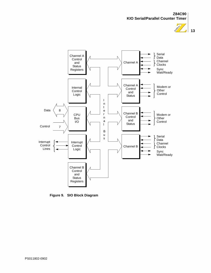
Figure 9. SIO Block Diagram
Data
Control
Serial
Channel
InterruptControl
Lines
Internal
Bus
Data
ClocksSyncWait/Ready
Modem orOtherControl
Modem orOtherControl
Serial
ChannelData
ClocksSyncWait/Ready
Channel AControl
andStatus
Registers
InternalControlLogic
CPUBusI/O
InterruptControlLogic
Channel BControl
andStatus
Registers
Channel A
Channel B
Channel AControl
andStatus
Channel BControl
andStatus
8
7
PS011802-0902
Z84C90KIO Serial/Parallel Counter Timer
14
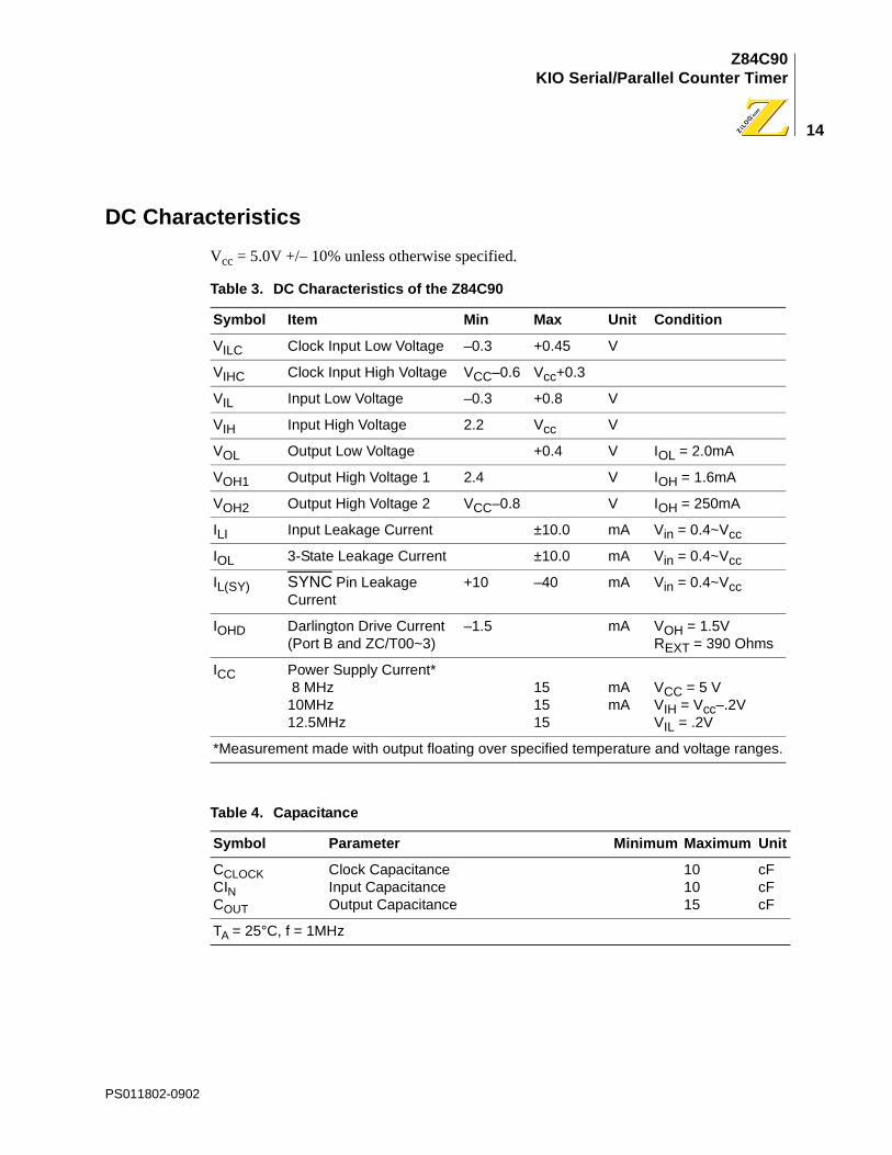
DC CharacteristicsVcc = 5.0V +/– 10% unless otherwise specified.
Table 3. DC Characteristics of the Z84C90
Symbol Item Min Max Unit Condition
VILC Clock Input Low Voltage –0.3 +0.45 V
VIHC Clock Input High Voltage VCC–0.6 Vcc+0.3
VIL Input Low Voltage –0.3 +0.8 V
VIH Input High Voltage 2.2 Vcc V
VOL Output Low Voltage +0.4 V IOL = 2.0mA
VOH1 Output High Voltage 1 2.4 V IOH = 1.6mA
VOH2 Output High Voltage 2 VCC–0.8 V IOH = 250mA
ILI Input Leakage Current ±10.0 mA Vin = 0.4~Vcc
IOL 3-State Leakage Current ±10.0 mA Vin = 0.4~Vcc
IL(SY) SYNC Pin Leakage Current
+10 –40 mA Vin = 0.4~Vcc
IOHD Darlington Drive Current(Port B and ZC/T00~3)
–1.5 mA VOH = 1.5VREXT = 390 Ohms
ICC Power Supply Current* 8 MHz10MHz12.5MHz
15 15 15
mAmA
VCC = 5 VVIH = Vcc–.2VVIL = .2V
*Measurement made with output floating over specified temperature and voltage ranges.
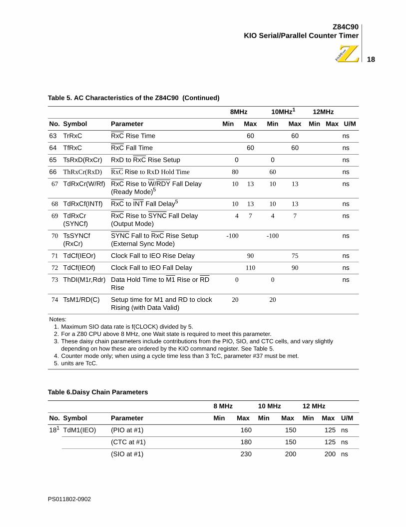
46 TdCf(ZCf) Clock Fall to ZC/TO Fall Delay 80 80 ns
SIO Timing
47 TdIOf(W/Rf) IORQ Fall to WT/RDY Fall Delay (Wait Mode)
130 110 ns
48 TdCr(W/Rf) Clock Rise to WT/RDY Delay (Ready Mode)
85 85 ns
49 TdCf(W/Rz) Clock Fall to WT/RDY Float Delay (Wait Mode)
90 80 ns
50 TwPh Pulse Width High 150 120 ns
51 TwPI Pulse Width Low 150 120 ns
52 TcTxC TxC Cycle Time 250 DC 200 DC ns
53 TwTxCh TxC Width High 85 DC 80 DC ns
54 TwTxCl TxC Width Low 85 DC 80 DC ns
55 TrTxC TxC Rise Time 60 60 ns
56 TfTxC TxC Fall Time 60 60 ns
57 TdTxCf(TxD) TxC Fall to TxD Delay (x1 mode) 160 120 ns
58 TdTxCf(W/Rf) TxC Fall to WT/RDY Fall Delay (Ready Mode)5
5 9 5 9 ns
59 TdTxCf(INTf) TxC Fall to INT Fall Delay5 5 9 5 9 ns
60 TcRxC RxC Cycle Time 250 DC 200 DC ns
61 TwRxCh RxC Width High 85 DC 80 DC ns
62 TwRxCl RxC Width Low 85 DC 80 DC ns
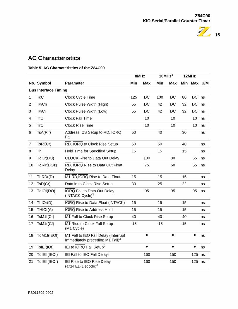
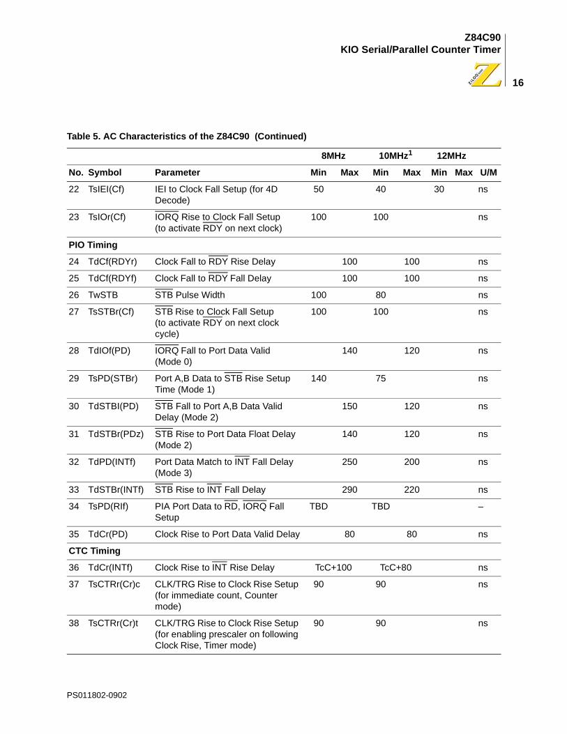
Table 5. AC Characteristics of the Z84C90 (Continued)
8MHz 10MHz1 12MHz
No. Symbol Parameter Min Max Min Max Min Max U/M
PS011802-0902
Z84C90KIO Serial/Parallel Counter Timer
18
63 TrRxC RxC Rise Time 60 60 ns
64 TfRxC RxC Fall Time 60 60 ns
65 TsRxD(RxCr) RxD to RxC Rise Setup 0 0 ns
66 ThRxCr(RxD) RxC Rise to RxD Hold Time 80 60 ns
67 TdRxCr(W/Rf) RxC Rise to W/RDY Fall Delay (Ready Mode)5
10 13 10 13 ns
68 TdRxCf(INTf) RxC to INT Fall Delay5 10 13 10 13 ns
69 TdRxCr(SYNCf)
RxC Rise to SYNC Fall Delay (Output Mode)
4 7 4 7 ns
70 TsSYNCf(RxCr)
SYNC Fall to RxC Rise Setup (External Sync Mode)
-100 -100 ns
71 TdCf(IEOr) Clock Fall to IEO Rise Delay 90 75 ns
72 TdCf(IEOf) Clock Fall to IEO Fall Delay 110 90 ns
73 ThDI(M1r,Rdr) Data Hold Time to M1 Rise or RD Rise
0 0 ns
74 TsM1/RD(C) Setup time for M1 and RD to clock Rising (with Data Valid)
20 20
Notes: 1. Maximum SIO data rate is f(CLOCK) divided by 5.2. For a Z80 CPU above 8 MHz, one Wait state is required to meet this parameter.3. These daisy chain parameters include contributions from the PIO, SIO, and CTC cells, and vary slightly
depending on how these are ordered by the KIO command register. See Table 5.4. Counter mode only; when using a cycle time less than 3 TcC, parameter #37 must be met.5. units are TcC.
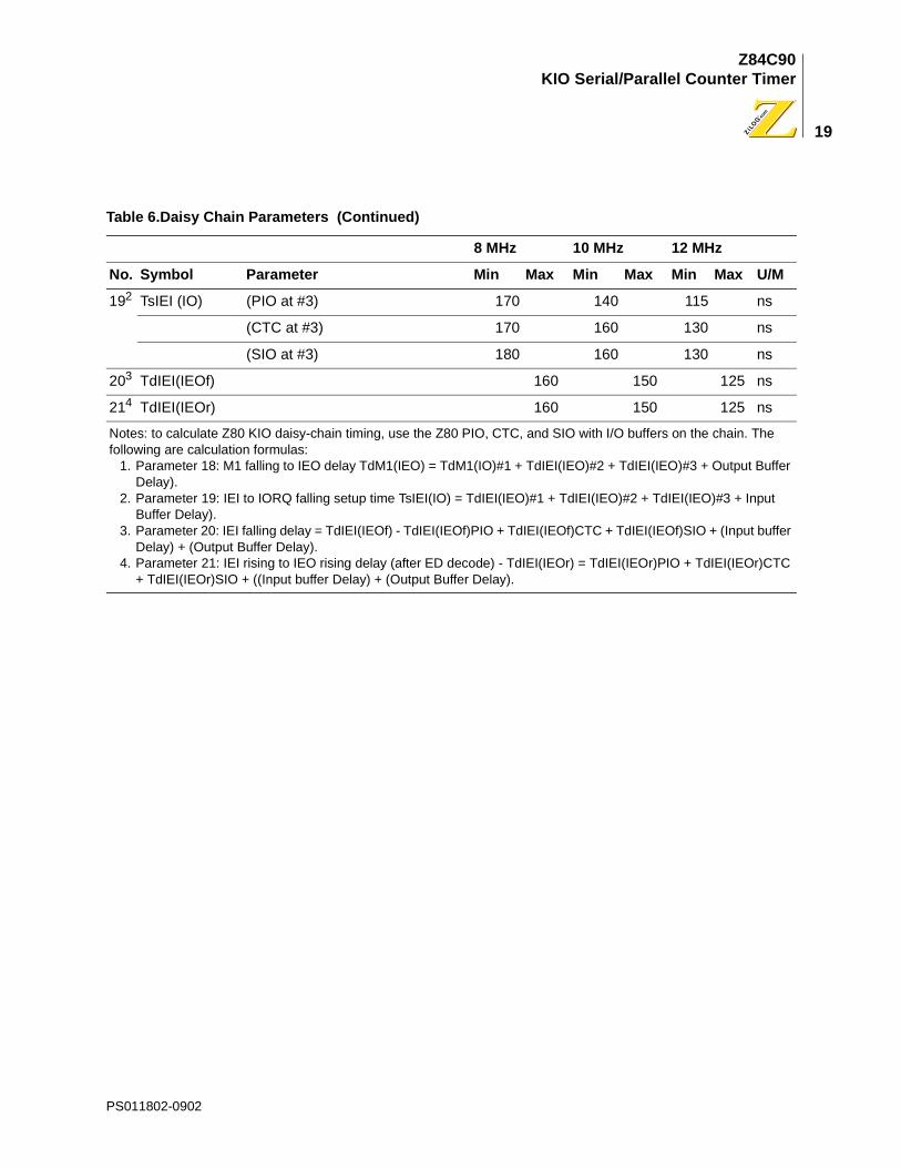
Table 6.Daisy Chain Parameters
8 MHz 10 MHz 12 MHz
No. Symbol Parameter Min Max Min Max Min Max U/M
181 TdM1(IEO) (PIO at #1) 160 150 125 ns
(CTC at #1) 180 150 125 ns
(SIO at #1) 230 200 200 ns
Table 5. AC Characteristics of the Z84C90 (Continued)
8MHz 10MHz1 12MHz
No. Symbol Parameter Min Max Min Max Min Max U/M
PS011802-0902
Z84C90KIO Serial/Parallel Counter Timer
19
192 TsIEI (IO) (PIO at #3) 170 140 115 ns
(CTC at #3) 170 160 130 ns
(SIO at #3) 180 160 130 ns
203 TdIEI(IEOf) 160 150 125 ns
214 TdIEI(IEOr) 160 150 125 ns
Notes: to calculate Z80 KIO daisy-chain timing, use the Z80 PIO, CTC, and SIO with I/O buffers on the chain. The following are calculation formulas:
Precautions & LimitationsThe following describe the limitations of Revision A of the Z84C90 KIO.
Problem:
Daisy-chain. If the KIO has an Interrupt Pending during and Interrupt Acknowledge cycle, KIO misses the status of the IE1 pin. This produces vector contention if there is a higher interrupting device. It works fine if only one device is in the system.
Work Around:
There is no problem if the application has only one peripheral in the daisy chain. For two or more peripherals in the system, a “hardware workaround circuit” is needed. Please con-tact your local Zilog representatives to get more detailed information.
Problem:
Reset. KIO requires the M1 signal to exit from Reset state. If the M1 signal is not received, the KIO can not be programmed. This is not a problem for users of the Z80 CPU.
Workaround:
If the CPU is other than a Z80, an M1 signal is needed to exit RESET status. Otherwise, the KIO can not be programmed.
Problem:
Port C. When Port C is used as Parallel I/O (not as SIO’s modem signals) and there is a status change on PC1 or PC6, the status of SYNCA or SYNCB (SIO cell) also changes.
Work Around:
Before using Port C as a parallel port, set the SIO modem signal mode back to Port C. This procedure avoids the problem.
Problem:
Interrupt Acknowledge cycle. The KIO modifies the contents of the KIO control register (specifically, the KIO modifies the daisy-chain configuration) if the CE pin is active dur-ing the Interrupt Acknowledge cycle (with other conditions satisfied).
PS011802-0902
Z84C90KIO Serial/Parallel Counter Timer
26
Work Around:This problem could happen under the following narrowly defined conditions:
• CE signal is active throughout the Interrupt Acknowledge cycle.
• The address on the bus, A3–A0, is “110b”.
• During this time, bit D3 is 1.
• At the end of the Interrupt Acknowledge cycle, M1 goes inactive prior to the IORQ signal.
• At the time period of CE active, IORQ active, and M1 returns to the inactive state; all during the rising edge of the clock.
This problem is not the case with the Z80 CPU. However, other CPUs could be affected. One of the possible workarounds is to add the condition M1 not active to generate a CE signal.