1 Kinetis L seriesThe Kinetis L series is the most scalable portfolio of ultra low-power, mixed-signal ARM® Cortex®-M0+ MCUs in theindustry. The portfolio includes five MCU families that offer abroad range of memory, peripheral and package options.Kinetis L Series families share common peripherals and pin-counts allowing developers to migrate easily within an MCUfamily or between MCU families to take advantage of morememory or feature integration. This scalability allowsdevelopers to standardize on the Kinetis L Series for their endproduct platforms, maximising hardware and software reuseand reducing time-to-market.
Features common to all Kinetis L series families include:• 48 MHz ARM Cortex-M0+ core• High-speed 12/16-bit analog-to-digital converters• 12-bit digital-to-analog converters for all series except
for KLx4/KLx2 family• High-speed analog comparators• Low-power touch sensing with wake-up on touch from
reduced power states for all series except for KLx4/KLx2 family
• Powerful timers for a broad range of applicationsincluding motor control
• Low-power focused serial communication interfacessuch as low-power UART, SPI, I2C, and others.
• Single power supply: 1.71–3.6 V with multiple low-power modes support single operation temperature:
Freescale Semiconductor Document Number:KL0xPB
Product Brief Rev 3.3, 07/2013
KL02/KL04/KL05 Product BriefSupports all KL02, KL04 and KL05 devices
• –40 ~ 105 °C (exclude WLCSP package)• –40 ~ 85 °C (WLCSP package)
Kinetis L series MCU families combine the latest low-power innovations with precision mixed-signal capability and a broadrange of communication, connectivity, and human-machine interface peripherals. Each MCU family is supported by amarket-leading enablement bundle from Freescale and numerous ARM third party ecosystem partners. The KL0x family isthe entry-point to the Kinetis L series and is pin-compatible with the 8-bit S08PT family. The KL1x/2x/3x/4x families arecompatible with each other and their equivalent ARM Cortex-M4 Kinetis K series families—K10/20/30/40.
The following figure depicts key features, memory and package options for Kinetis L series family of MCUs.
KL2x Family
KL1x Family
KL0x Family
KL3x Family
Family Program Flash
Packages Key Features
Low power Mixed signal USB Segment LCD
KL4x Family
8-32KB
32-256KB
32-256KB
64-256KB
128-256KB
16-48pin
32-80pin
32-121pin
64-121pin
64-121pin
Figure 1. Kinetis L series families of MCU portfolio
All Kinetis L series families include a powerful array of analog, communication and timing and control peripherals with thelevel of feature integration increasing with flash memory size and the pin count. Features within the Kinetis L series familiesinclude:
• Core and architecture:• ARM Cortex-M0+ Core running up to 48 MHz with zero wait state execution from memories
• Single-cycle access to I/O: Up to 50 percent faster than standard I/O, improves reaction time to externalevents allowing bit banging and software protocol emulation
• Two-stage pipeline: Reduced number of cycles per instruction (CPI), enabling faster branch instruction andISR entry, and reducing power consumption
• Excellent code density as compared to 8-bit and 16-bit MCUs: Reduces flash size, system, cost and powerconsumption
• Optimized access to program memory: Accesses on alternate cycles reduces power consumption.• 100 percent compatible with ARM Cortex-M0 and a subset ARM Cortex-M3/M4: Reuse existing
compilers and debug tools.• Simplified architecture: 56 instructions and 17 registers enable easy programming and efficient packaging
of 8/16/32-bit data in memory.• Linear 4 GB address space removes the need for paging/banking, reducing software complexity.• ARM third-party ecosystem support: Software and tools to help minimize development time/cost
• Micro Trace Buffer: Lightweight trace solution allows fast bug identification and correction.
Kinetis L series
KL02/KL04/KL05 Product Brief, Rev 3.3, 07/2013
2 Freescale Semiconductor, Inc.
• Bit Manipulation Engine (BME): BME reduces code size and cycles for bit-oriented operations to peripheralregisters eliminating traditional methods where the core would need to perform read-modify-write operations.
• Up to 4-channel DMA for peripheral and memory servicing with minimal CPU intervention (feature not availableon KL02 family)
• Ultra low-power:• Extreme dynamic efficiency: 32-bit ARM Cortex-M0+ core combined with Freescale 90 nm thin-film storage
flash technology delivers 50% energy savings per Coremark in comparison to the closest 8/16-bit competitivesolution.
• Multiple flexible low-power modes, including new operation clocking option which reduces dynamic power byshutting off bus and system clocks for lowest power core processing. Peripherals with an alternate asynchronousclock source can continue operation.
• UART, SPI, I2C, ADC, DAC, TPM, LPTMR, and DMA support low-power mode operation without waking upthe core (DMA is not available on KL02).
• Memory:• Scalable memory footprints from 8 KB flash / 1 KB SRAM to 256 KB flash / 32 KB SRAM• Embedded 64 B cache memory for optimizing bus bandwidth and flash execution performance (32 B cache on
KL02 family)• Mixed-signal analog:
• Fast, high-precision 16-, or 12-bit ADC with optional differential pairs, 12-bit DAC, high-speed comparators.• Powerful signal conditioning, conversion, and analysis capability with reduced system cost (12-bit DAC not
available on KL02 family)• Human Machine Interface (HMI):
• Optional capacitive Touch Sensing Interface with full low-power support and minimal current adder whenenabled
• Segment LCD controller• Connectivity and communications:
• Up to three UARTs:• All UARTs support DMA transfers, and can trigger when data on bus is detected;• UART0 supports 4x to 32x over sampling ratio;• Asynchronous transmit and receive operation for operating in STOP/VLPS modes.
• Up to two SPIs• Up to two I2Cs• Full-speed USB OTG controller with on-chip transceiver• 3.3–5 V USB on-chip regulator• Up to one I2S
• Reliability, safety, and security:• Internal watchdog with independent clock source
• Timing and control:• Powerful timer modules which support general-purpose, PWM, and motor control functions• Periodic Interrupt Timer for RTOS task scheduler time base or trigger source for ADC conversion and timer
modules• System:
• GPIO with pin interrupt functionality• Wide operating voltage range from 1.71 V to 3.6 V with flash programmable down to 1.71 V with fully
functional flash and analog peripherals• Ambient operating temperature ranges from –40 °C to 85 °C for WLCSP package and 105 °C for all the other
packages
2 KL02/KL04/KL05 sub-family introductionThe device is highly-integrated, market leading ultra low-power 32-bit microcontroller based on the enhanced Cortex-M0+(CM0+) core platform. The features of the KL0x family derivatives are as follows.
• Core platform clock up to 48 MHz, bus clock up to 24 MHz
KL02/KL04/KL05 sub-family introduction
KL02/KL04/KL05 Product Brief, Rev 3.3, 07/2013
Freescale Semiconductor, Inc. 3
• Memory option is up to 32 KB Flash and 4 KB RAM• Wide operating voltage ranges from 1.71–3.6 V with fully functional flash program/erase/read operations• Multiple package options from 24-pin to 48-pin for KL04 and KL05• Ambient operating temperature ranges from –40 °C to 85 °C for WLCSP package and –40 °C to 105 °C for all the
others.
The family acts as an ultra low-power, cost-effective microcontroller to provide developers an appropriate entry-level 32-bitsolution. The family is the next-generation MCU solution for low-cost, low-power, high-performance devices applications.It’s valuable for cost-sensitive, portable applications requiring long battery life-time.
3 Block diagramThe following figure shows a superset block diagram of the device. Other devices within the family have a subset of thefeatures.
Memories and Memory Interfaces
Programflash
RAM
Analog Timers Communication Interfaces
SPIx1
Clocks
Frequency-
Core
Debuginterfaces
Interruptcontroller
Human-MachineInterface (HMI)
System
Internalwatchdog locked loop
referenceInternal
clocks
oscillator
Lowfrequency
Low powerUART
x1
Cortex-M0+ARM
withGPIOs
interruptLow Power
Timer
MTB
BME
6-bit DAC
comparatorx1
Analog
watchdog
Securityand Integrity
Internal
Kinetis KL02 Family
x2I C2
Timers2x2ch
12-bit ADCx1
Figure 2. KL02 family block diagram
Block diagram
KL02/KL04/KL05 Product Brief, Rev 3.3, 07/2013
4 Freescale Semiconductor, Inc.
Memories and Memory Interfaces
Programflash
RAM
6-bit DAC
watchdog
Analog Timers Communication Interfaces
Securityand Integrity
SPIx1
Lowpower timer
Clocks
Frequency-
Core
Debuginterfaces
Interruptcontroller
comparatorx1
Analog
Human-MachineInterface (HMI)
System
DMA
Internalwatchdog locked loop
referenceInternal
clocks
timersinterruptPeriodic
oscillator
Low/highfrequency
Low powerUART
x1
Cortex-M0+ARM
withGPIOs
interrupt
BME MTB
RTC
Internal
Kinetis KL04 Family
LEGEND
x1I C2
x1
Timers1x6ch+1x2ch
12-bit ADCx1
Figure 3. KL04 family block diagram
Block diagram
KL02/KL04/KL05 Product Brief, Rev 3.3, 07/2013
Freescale Semiconductor, Inc. 5
Memories andMemory Interfaces
Programflash
RAM
6-bit DAC
Analog Timers CommunicationInterfaces
Securityand Integrity
SPIx1
Lowpower timer
Clocks
Frequency-
Core
Debuginterfaces
Interruptcontroller
comparatorx1
Analog
Human-MachineInterface (HMI)
System
DMA
Internalwatchdog locked loop
referenceInternal
clocks
timersinterruptPeriodic
oscillator
Low/highfrequency
Low powerUART
x1
Cortex-M0+ARM
withGPIOs
interrupt
Kinetis KL05 Family
LEGEND
x1I C2
x1
Timers1x6ch+1x2ch
12-bit ADCx1
TSI
12-bit DAC
BMEMTB
RTC
watchdogInternal
Figure 4. KL05 family block diagram
Block diagram
KL02/KL04/KL05 Product Brief, Rev 3.3, 07/2013
6 Freescale Semiconductor, Inc.
Features
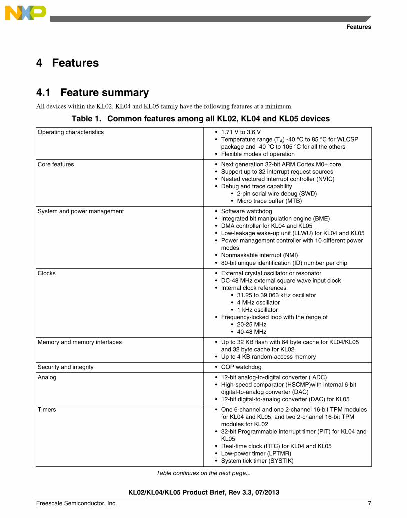
4.1 Feature summaryAll devices within the KL02, KL04 and KL05 family have the following features at a minimum.
Table 1. Common features among all KL02, KL04 and KL05 devices
Operating characteristics • 1.71 V to 3.6 V• Temperature range (TA) -40 °C to 85 °C for WLCSP
package and -40 °C to 105 °C for all the others• Flexible modes of operation
Core features • Next generation 32-bit ARM Cortex M0+ core• Support up to 32 interrupt request sources• Nested vectored interrupt controller (NVIC)• Debug and trace capability
• 2-pin serial wire debug (SWD)• Micro trace buffer (MTB)
System and power management • Software watchdog• Integrated bit manipulation engine (BME)• DMA controller for KL04 and KL05• Low-leakage wake-up unit (LLWU) for KL04 and KL05• Power management controller with 10 different power
modes• Nonmaskable interrupt (NMI)• 80-bit unique identification (ID) number per chip
digital-to-analog converter (DAC)• 12-bit digital-to-analog converter (DAC) for KL05
Timers • One 6-channel and one 2-channel 16-bit TPM modulesfor KL04 and KL05, and two 2-channel 16-bit TPMmodules for KL02
• 32-bit Programmable interrupt timer (PIT) for KL04 andKL05
• Real-time clock (RTC) for KL04 and KL05• Low-power timer (LPTMR)• System tick timer (SYSTIK)
Table continues on the next page...
4
Features
KL02/KL04/KL05 Product Brief, Rev 3.3, 07/2013
Freescale Semiconductor, Inc. 7
Table 1. Common features among all KL02, KL04 and KL05 devices (continued)
Communications • SPI with DMA support1
• I2C with DMA support2
• Low-power UART with DMA support2
Human-machine interface • GPIO with pin interrupt support, DMA requestcapability, and other pin control options2
• Capacitive touch sensing inputs for KL05
1. KL02 does not support DMA.2. KL02 does not support DMA feature.
4.2 Memory and package optionsThe following table summarizes the memory and package options for the KL0x family. All devices which share a commonpackage are pin-for-pin compatible.
Table 2. KL0x family summary
Su
b-F
amily
Per
form
ance
(M
Hz)
Memory Package
Fla
sh (
KB
)
SR
AM
(KB
)
16 Q
FN
(3x
3)
20 C
SP
(2x
2)
24 Q
FN
(4x
4)
32 L
QF
P (
7x7)
32 Q
FN
(5x
5)
48 L
QF
P (
7x7)
KL02 48 8 1 + — — — — —
48 16 2 + — + — + —
48 32 4 + + + — + —
KL04 48 8 1 — — + + + —
48 16 2 — — + + + +
48 32 4 — — + + + +
KL05 48 8 1 — — + + + —
48 16 2 — — + + + +
48 32 4 — — + + + +
4.3 Part numbers and packaging
Features
KL02/KL04/KL05 Product Brief, Rev 3.3, 07/2013
8 Freescale Semiconductor, Inc.
Q KL## A FFF T PP CC (N)
Qualification status
Family
Flash size
Temperature range (°C)
Speed (MHz)
Package identifier
Tape and Reel (T&R)
Key attribute
Figure 5. Part numbers diagrams
Table 3. Part number fields descriptions
Field Description Values
Q Qualification status • M = Fully qualified, general market flow, 3000pieces reels
• P = Prequalification• K = Fully qualified, general market flow, 100
R Silicon revision • (Blank) = Main• A = Revision after main
T Temperature range (°C) • C = –40 to 85
PP Package identifier • FG = 16 QFN (3 mm x 3 mm)• AF = 20 WLCSP (1.99 mm x 1.94 mm)• FK = 24 QFN (4 mm x 4 mm)• LC = 32 LQFP (7 mm x 7 mm)• FM = 32 QFN (5 mm x 5 mm)• LF = 48 LQFP (7 mm x 7 mm)
CC Maximum CPU frequency (MHz) • 4 = 48 MHz
N Packaging type • R = Tape and reel• (Blank) = Trays
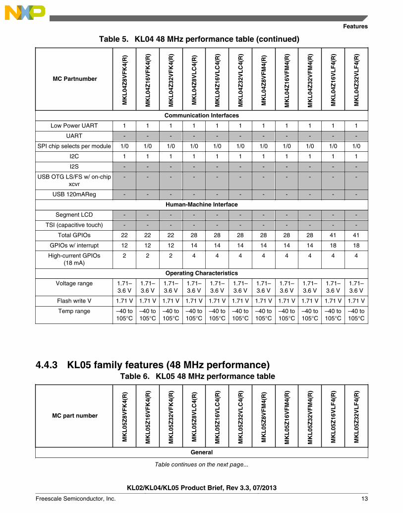
4.4 KL02/KL04/KL05 family featuresThe following sections list the differences among the various devices available within the KL02/KL04/KL05 family.
The features listed for each part number in the following subsection specify the maximum configuration available on thatdevice. The signal multiplexing configuration determines which modules can be used simultaneously.
Features
KL02/KL04/KL05 Product Brief, Rev 3.3, 07/2013
Freescale Semiconductor, Inc. 9
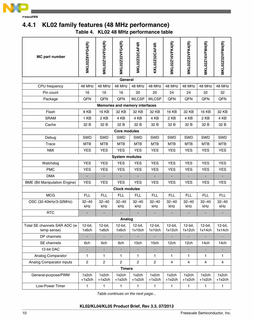
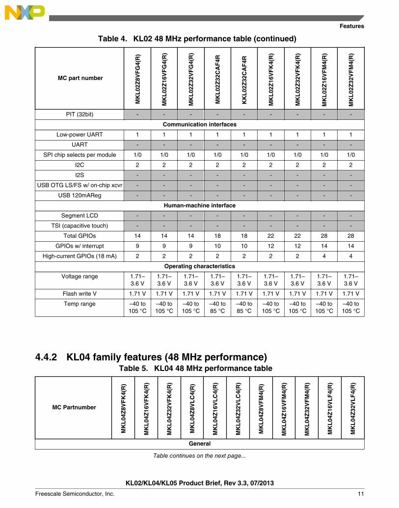
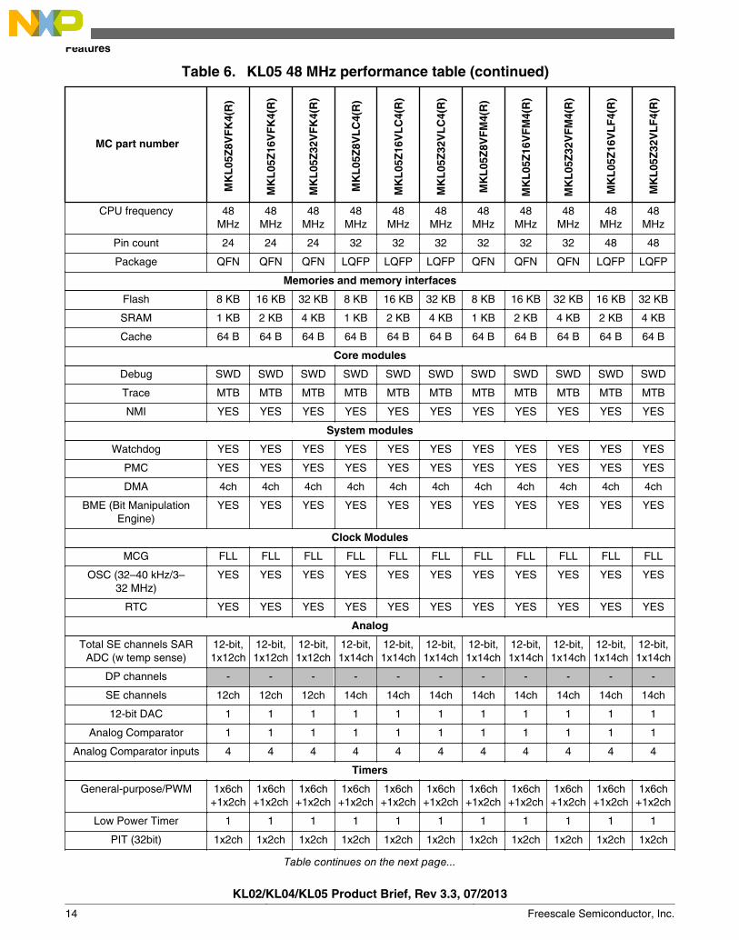
4.4.1 KL02 family features (48 MHz performance)Table 4. KL02 48 MHz performance table
MC part number
MK
L02
Z8V
FG
4(R
)
MK
L02
Z16
VF
G4(
R)
MK
L02
Z32
VF
G4(
R)
MK
L02
Z32
CA
F4R
KK
L02
Z32
CA
F4R
MK
L02
Z16
VF
K4(
R)
MK
L02
Z32
VF
K4(
R)
MK
L02
Z16
VF
M4(
R)
MK
L02
Z32
VF
M4(
R)
General
CPU frequency 48 MHz 48 MHz 48 MHz 48 MHz 48 MHz 48 MHz 48 MHz 48 MHz 48 MHz
Flash write V 1.71 V 1.71 V 1.71 V 1.71 V 1.71 V 1.71 V 1.71 V 1.71 V 1.71 V 1.71 V 1.71 V
Temp range –40 to105°C
–40 to105°C
–40 to105°C
–40 to105°C
–40 to105°C
–40 to105°C
–40 to105°C
–40 to105°C
–40 to105°C
–40 to105°C
–40 to105°C
4.5 Module-by-module feature listThe following sections describe the high-level module features for the family's superset device. See KL02/KL04/KL05family features for differences among the subset devices.
Core modules
4.5.1.1 ARM Cortex M0+ core• Up to 48 MHz core frequency from 1.71 V to 3.6 V across temperature range of –40 °C to 105 °C• Support up to 32 interrupt request sources• 2-stage pipeline microarchitecture for reduced power consumption and improved architectural performance (cycles per
instruction)
4.5.1
Core modules
KL02/KL04/KL05 Product Brief, Rev 3.3, 07/2013
Freescale Semiconductor, Inc. 15
• Binary compatible instruction set architecture with the CM0 core• Thumb instruction set combines high code density with 32-bit performance.• Serial wire debug (SWD) reduces the number of pins required for debugging.• Micro trace buffer (MTB) provides lightweight program trace capabilities using system RAM as the destination
• Up to 32 interrupt sources• Includes a single nonmaskable interrupt
4.5.1.3 Wake-Up Interrupt Controller (WIC)
• Supports interrupt handling when system clocking is disabled in low power modes• Takes over and emulates the NVIC behavior when correctly primed by the NVIC on entry to Very-Deep-Sleep mode• A rudimentary interrupt masking system with no prioritization logic signals for wake-up as soon as a nonmasked
interrupt is detected.• Contains no programmer’s model visible state and is therefore invisible to end users of the device other than through
the benefits of reduced power consumption while sleeping
4.5.1.4 Debug Controller• 2-pin serial wire debug (SWD) provides external debugger interface• Micro trace buffer (MTB) provides simple execution trace capability and operates as a simple AHB-Lite SRAM
controller.
System modules
4.5.2.1 Power Management Control Unit (PMC)
• Separate digital (regulated) and analog (referenced to digital) supply outputs• Programmable power saving modes• No output supply decoupling capacitors required• Available wake-up from power saving modes via RTC and external inputs• Integrated Power-on Reset (POR)• Integrated Low Voltage Detect (LVD) with reset (brownout) capability• Selectable LVD trip points• Programmable Low Voltage Warning (LVW) interrupt capability• Buffered bandgap reference voltage output• Factory programmed trim for bandgap and LVD• 1 kHz Low-Power Oscillator (LPO)
4.5.2.2 DMA Channel Multiplexer (DMA MUX)• Four independently selectable DMA channel routers• Two periodic trigger sources available• Each channel router can be assigned to 1 of 63 possible peripheral DMA sources.
4.5.2
System modules
KL02/KL04/KL05 Product Brief, Rev 3.3, 07/2013
16 Freescale Semiconductor, Inc.
4.5.2.3 DMA ControllerFour independently programmable DMA controller channels provide the means to directly transfer data between systemmemory and I/O peripherals.
• DMA controller is capable of functioning in Run, Wait, and Stop modes of operation.• Dual-address transfers via 32-bit master connection to the system bus• Data transfer in 8-, 16-, or 32-bit blocks• Continuous-mode or cycle-steal transfers from software or peripheral initiation
4.5.2.4 COP Watchdog module• Independent clock source input (independent from CPU/bus clock)• Choice between two clock sources
• LPO oscillator• Bus clock
4.5.2.5 System clocks• System Oscillator (XOSC)—Loop-control pierce oscillator; crystal or ceramic resonator range of 32 kHz to 40 kHz
(low range mode) or 3-32 MHz (high range mode)• Multipurpose Clock Generator (MCG)
• Frequency-locked loop (FLL) controlled by internal or external reference• 20~40 MHz FLL output• 40~48 MHz FLL output
• Internal reference clocks—Can be used as a clock source for other on-chip peripherals• On-chip RC oscillator range of 31.25 kHz to 39.0625 kHz with 0.2% trim step and 1% accuracy across
temperature range of 0 °C to 70 °C and 2% accuracy across full temperature range• On-chip RC oscillator range of 31.25 kHz to 39.0625 kHz with 0.2% trim step and 1% accuracy across full
temperature range• Ultra low-power 4 MHz IRC
Memories and memory interfaces
4.5.3.1 On-chip memory
• 48 MHz performance devices• Up to 32 KB program flash memory• Up to 4 KB SRAM
• Security circuitry to prevent unauthorized access to RAM and flash memory contents
Analog
4.5.4.1 Analog-to-Digital Converter (ADC)• Linear successive approximation algorithm with up to 16-bit resolution• Output modes:
• Single-ended 12-bit, 10-bit, and 8-bit modes, in right-aligned unsigned format• Single or continuous conversion• Configurable sample time and conversion speed/power• Conversion complete and hardware average complete flag and interrupt
4.5.3
4.5.4
Memories and memory interfaces
KL02/KL04/KL05 Product Brief, Rev 3.3, 07/2013
Freescale Semiconductor, Inc. 17
• Input clock selectable from up to four sources• Operation in low-power modes for lower noise operation• Asynchronous clock source for lower noise operation with option to output the clock• Selectable asynchronous hardware conversion trigger with hardware channel select• Automatic compare with interrupt for various programmable values• Temperature sensor• Hardware average function• Selectable voltage reference• Self-calibration mode
4.5.4.2 High-Speed Analog Comparator (CMP)• 6-bit DAC programmable reference generator output• Up to five selectable comparator inputs; each input can be compared with any input by any polarity sequence• Selectable interrupt on rising-edge, falling-edge, or either rising or falling edges of the comparator output• Comparator output supports:
• Sampled• Windowed (ideal for certain PWM zero-crossing-detection applications• Digitally filtered using external sample signal or scaled peripheral clock
• Two performance modes:• Shorter propagation delay at the expense of higher power• Low power, with longer propagation delay
• Operational in all MCU power modes except for VLLS0
4.5.4.3 12-bit Digital-to-Analog Converter (DAC)• 12-bit resolution• Guaranteed 6-sigma monotonicity over input word• High- and low-speed conversions
• 1 μs conversion rate for high speed, 2 μs for low speed• Power-down mode• Automatic mode allows the DAC to generate its own output waveforms including square, triangle, and sawtooth.• Automatic mode allows programmable period, update rate, and range.• DMA support
Timers
4.5.5.1 Timer/PWM (TPM)• Selectable source clock• Programmable prescaler• 16-bit counter supporting free-running or initial/final value, and counting is up or up-down• Input capture, output compare, and edge-aligned and center-aligned PWM modes• Input capture and output compare modes• Generation of hardware triggers• DMA support for TPM events
4.5.5.2 Periodic Interrupt Timers (PITs)
• Two general-purpose interrupt timers• Two interrupt timers for triggering ADC conversions• 32-bit counter resolution
4.5.5
Timers
KL02/KL04/KL05 Product Brief, Rev 3.3, 07/2013
18 Freescale Semiconductor, Inc.
• Clocked by bus clock frequency• DMA support
4.5.5.3 Real-Time Clock (RTC)• 32-bit seconds counter with 32-bit alarm• 16-bit prescaler with compensation• Register write protection• Hard Lock requires MCU POR to enable write access
Communication interfaces
4.5.6.1 Inter-Integrated Circuit (I2C)• Compatible with I2C bus standard and SMBus Specification Version 2 features• Up to 400 kbit/s with maximum bus loading• Multimaster operation• Software programmable for one of 64 different serial clock frequencies• Programmable slave address and glitch input filter• Interrupt or DMA driven byte-by-byte data transfer• Arbitration lost interrupt with automatic mode switching from master to slave• Calling address identification interrupt• Bus busy detection broadcast and 10-bit address extension• Address matching causes wake-up when the processor is in low-power mode.
4.5.6.2 UART0• Full-duplex operation• Standard mark/space non-return-to-zero (NRZ) format• 13-bit baud rate selection with fractional divide of 32• Programmable 8-bit or 9-bit data format• Separately enabled transmitter and receiver• Programmable transmitter output polarity• Programmable receive input polarity• 13-bit break character option• 11-bit break character detection option• Two receiver wake-up methods:
• Idle line wake-up• Address mark wake-up
• Address match feature in receiver to reduce address mark wake-up ISR overhead• Interrupt or DMA driven operation• Receiver framing error detection• Hardware parity generation and checking• Configurable oversampling ratio to support from 1/4 to 1/32 bit-time noise detection• Operation in low-power modes
4.5.6.3 Serial Peripheral Interface (SPI)• Master and slave mode• Full-duplex, three-wire synchronous transfers• Programmable transmit bit rate• Double-buffered transmit and receive data registers• Serial clock phase and polarity options
4.5.6
Communication interfaces
KL02/KL04/KL05 Product Brief, Rev 3.3, 07/2013
Freescale Semiconductor, Inc. 19
• Slave select output• Mode fault error flag with CPU interrupt capability• Control of SPI operation during wait mode• Selectable MSB-first or LSB-first shifting• Support for both transmit and receive by DMA
Human-machine interface
4.5.7.1 General-Purpose Input/Output (GPIO)• Hysteresis and configurable pullup device on all input pins• Configurable drive strength on some output pins• Independent pin value register to read logic level on digital pin
4.5.7.2 Touch Sensor Input (TSI)• Supports up to 16 external electrodes• Automatic detection of electrode capacitance across all operational power modes• Internal reference oscillator for high-accuracy measurement• Configurable software or hardware scan trigger• Fully supports Freescale touch sensing software (TSS) library• Capability to wake the MCU from low-power modes• Compensate for temperature and supply voltage variations• High sensitivity change with 16-bit resolution register• Configurable up to 4096 scan times.• Support DMA data transfer
5 Power modesThe Power Management Controller (PMC) provides multiple power options to allow the user to optimize power consumptionfor the level of functionality needed.
Depending on the stop requirements of the user application, a variety of stop modes are available that provide state retention,partial power-down or full power-down of certain logic and/or memory. I/O states are held in all modes of operation. Thefollowing table compares the various power modes available.
For each run mode, there is a corresponding Wait and Stop mode. Wait modes are similar to ARM Sleep modes. Stop modes(VLPS, STOP) are similar to ARM Sleep Deep mode. The Very Low Power Run (VLPR) operating mode can drasticallyreduce runtime power when the maximum bus frequency is not required to handle the application needs.
The three primary modes of operation are Run, Wait, and Stop. The WFI instruction invokes both Wait and Stop modes forthe chip. The primary modes are augmented in a number of ways to provide lower power based on application needs.
• Default mode out of reset• On-chip voltage regulator is on.
Normal Wait -via WFI
Allows peripherals to function while the core is in Sleep mode,reducing power.
• NVIC remains sensitive to interrupts• Peripherals continue to be clocked.
Sleep Interrupt
Normal Stop -via WFI
Places chip in static state. Lowest power mode that retains all registerswhile maintaining LVD protection.
• NVIC is disabled.• AWIC is used to wake up from interrupt.• Peripheral clocks are stopped.
Sleep Deep Interrupt
VLPR (VeryLow-Power Run)
On-chip voltage regulator is in a low-power mode that supplies onlyenough power to run the chip at a reduced frequency. Only MCGmodes BLPI and BLPE can be used in VLPR.
• Reduced frequency Flash access mode (1 MHz)• LVD off• In BLPI clock mode, only the fast internal reference oscillator is
available to provide a low power nominal 4 MHz source for thecore with the nominal bus and flash clock required to be <800kHz
• Alternatively, BLPE clock mode can be used with an externalclock or the crystal oscillator providing the clock source.
Run —
VLPW (VeryLow-Power
Wait) -via WFI
Same as VLPR but with the core in Sleep mode to further reducepower.
• NVIC remains sensitive to interrupts (FCLK = ON).• On-chip voltage regulator is in a low-power mode that supplies
only enough power to run the chip at a reduced frequency.
Sleep Interrupt
VLPS (VeryLow-Power
Stop)-via WFI
Places chip in static state with LVD operation off. Lowest power modewith ADC and pin interrupts functional.
• Peripheral clocks are stopped, but OSC, LPTMR, RTC, CMP,TSI can be used.
• TPM and UART can optionally be enabled if their clock source isenabled.
• NVIC is disabled (FCLK = OFF); AWIC is used to wake up frominterrupt.
• On-chip voltage regulator is in a low-power mode that suppliesonly enough power to run the chip at a reduced frequency.
• All SRAM is operating (content retained and I/O states held).
Sleep Deep Interrupt
LLS1 (Low-Leakage Stop)
State retention power mode• Most peripherals are in state retention mode (with clocks
stopped), but OSC, LLWU,LPTMR, RTC, CMP, TSI can be used.• NVIC is disabled; LLWU is used to wake up.
NOTE: The LLWU interrupt must not be masked bythe interrupt controller to avoid a scenariowhere the system does not fully exit stopmode on an LLS recovery
• All SRAM is operating (content retained and I/O states held).
Sleep Deep Wake-upInterrupt2
VLLS3 (VeryLow-Leakage
Stop3)
• Most peripherals are disabled (with clocks stopped), but OSC,LLWU, LPTMR, RTC, CMP, TSI can be used.
• NVIC is disabled; LLWU is used to wake up.• SRAM_U and SRAM_L remain powered on (content retained
and I/O states held).
VLLS1 (VeryLow-Leakage
Stop1)
• Most peripherals are disabled (with clocks stopped), but OSC,LLWU, LPTMR, RTC, CMP, TSI can be used.
• NVIC is disabled; LLWU is used to wake up.• All of SRAM_U and SRAM_L are powered off.
Sleep Deep Wake-up Reset3
VLLS0 (VeryLow-Leakage
Stop 0)
• Most peripherals are disabled (with clocks stopped), but LLWU,LPTMR, RTC, TSI can be used.
• NVIC is disabled; LLWU is used to wake up.• All of SRAM_U and SRAM_L are powered off.• LPO disabled, optional POR brown-out detection
Sleep Deep Wake-up Reset3
1. KL02 does not support LLS mode.2. Resumes Normal Run mode operation by executing the LLWU interrupt service routine.3. Follows the reset flow with the LLWU interrupt flag set for the NVIC.
6 Revision historyThe following table provides a revision history for this document.
Table 8. Revision history
Rev. No. Date Substantial changes
1 3/16/2012 Initial publish
2 6/4/2012 Updated Kinetis KL series of MCU portfolio diagram.
Updated KL04 family block diagram.
Updated ADC feature for KL04.
Updated KL0x family summary table.
3 10/8/2012 Added KL02 family.
3.1 10/22/2012 Updated the feature in the section of Inter-Integrated Circuit (I2C) to "Up to400 kbit/s with maximum bus loading".
3.2 5/28/2013 Added WLCSP package for KL02.
3.3 7/1/2013 • Added KKL02Z32CAF4R.• Clarified KL02 has no LLWU.
Revision history
KL02/KL04/KL05 Product Brief, Rev 3.3, 07/2013
22 Freescale Semiconductor, Inc.
How to Reach Us:
Home Page:freescale.com
Web Support:freescale.com/support
Information in this document is provided solely to enable system andsoftware implementers to use Freescale products. There are no expressor implied copyright licenses granted hereunder to design or fabricateany integrated circuits based on the information in this document.Freescale reserves the right to make changes without further notice toany products herein.
Freescale makes no warranty, representation, or guarantee regardingthe suitability of its products for any particular purpose, nor doesFreescale assume any liability arising out of the application or use ofany product or circuit, and specifically disclaims any and all liability,including without limitation consequential or incidental damages.“Typical” parameters that may be provided in Freescale data sheetsand/or specifications can and do vary in different applications, andactual performance may vary over time. All operating parameters,including “typicals,” must be validated for each customer application bycustomer's technical experts. Freescale does not convey any licenseunder its patent rights nor the rights of others. Freescale sells productspursuant to standard terms and conditions of sale, which can be foundat the following address: freescale.com/SalesTermsandConditions.
Freescale, the Freescale logo, Energy Efficient Solutions logo, andKinetis are trademarks of Freescale Semiconductor, Inc., Reg. U.S. Pat.& Tm. Off. All other product or service names are the property of theirrespective owners. ARM and Cortex-M0+ are the registered trademarksof ARM Limited.