Klein Tunneling PHYS 503 Physics Colloquium Fall 2008 9/11 Deepak Rajput Graduate Research Assistant Center for Laser Applications University of Tennessee Space Institute Email: [email protected]Web: http://drajput.com
Transcript
1 of xx
Klein TunnelingPHYS 503 Physics Colloquium Fall 2008
9/11
Deepak RajputGraduate Research AssistantCenter for Laser ApplicationsUniversity of Tennessee Space InstituteEmail: [email protected]: http://drajput.com
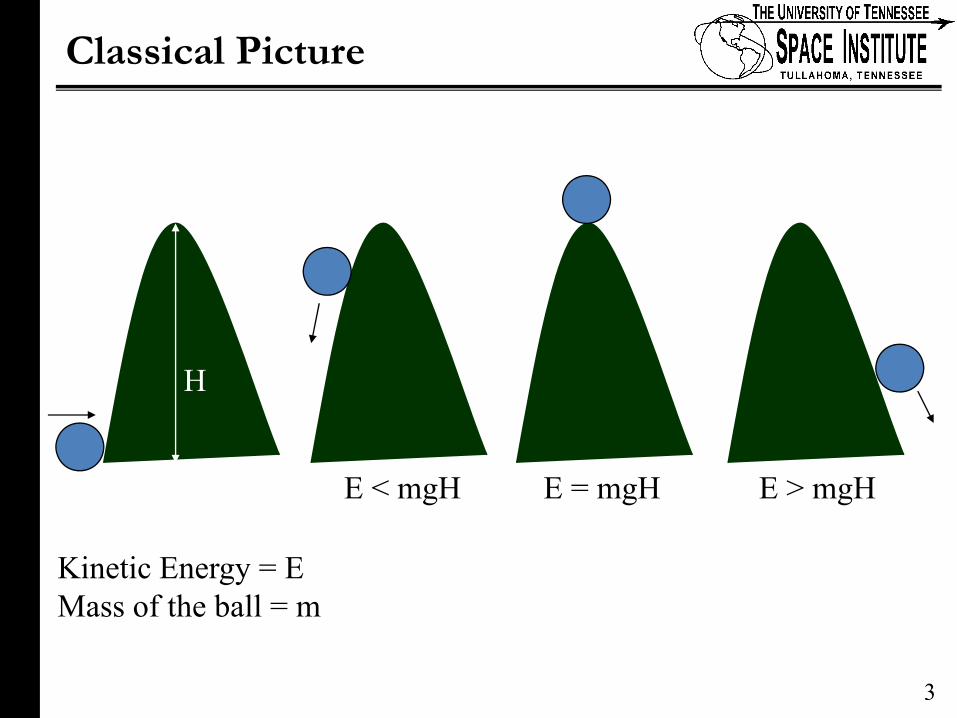
Transmission of a particle through a potential barrier higher than its kinetic energy (V>E).
It violates the principles of classical mechanics.
It is a quantum effect.
4
5 of xx
Quantum tunneling effect
On the quantum scale, objects exhibit wave-likecharacteristics.
Quanta moving against a potential hill can be described by their wave function.
The wave function represents the probability amplitudeof finding the object in a particular location.
5
6 of xx
Quantum tunneling effect
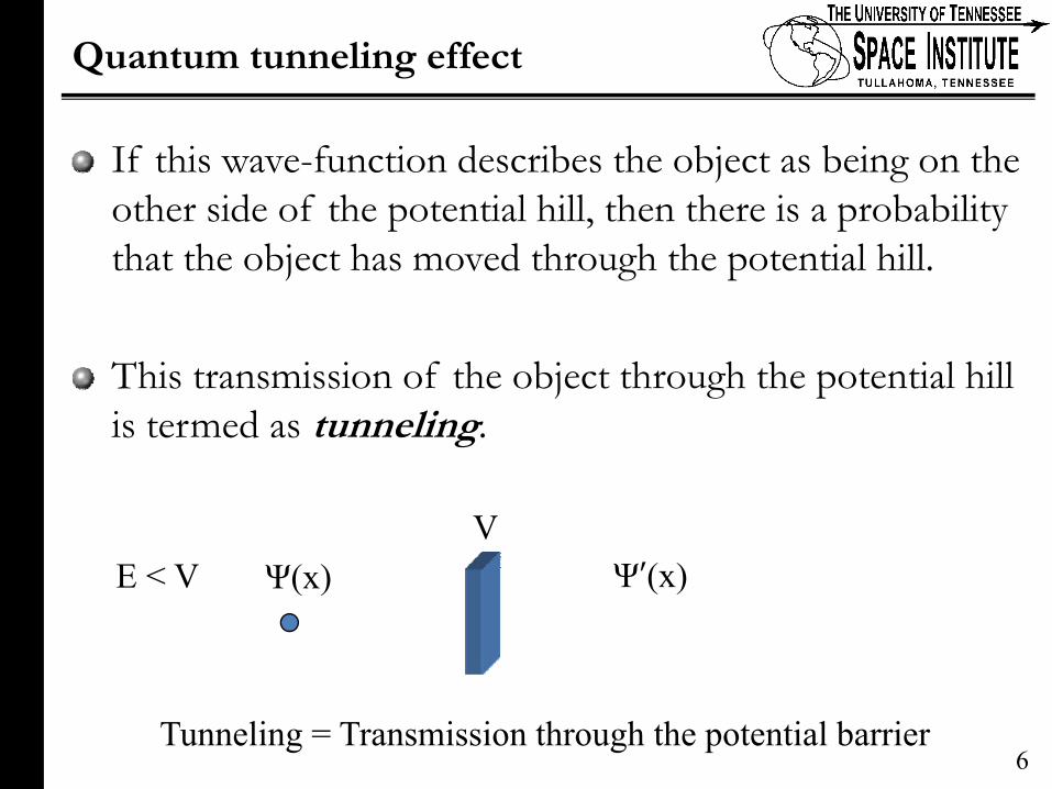
If this wave-function describes the object as being on the other side of the potential hill, then there is a probability that the object has moved through the potential hill.
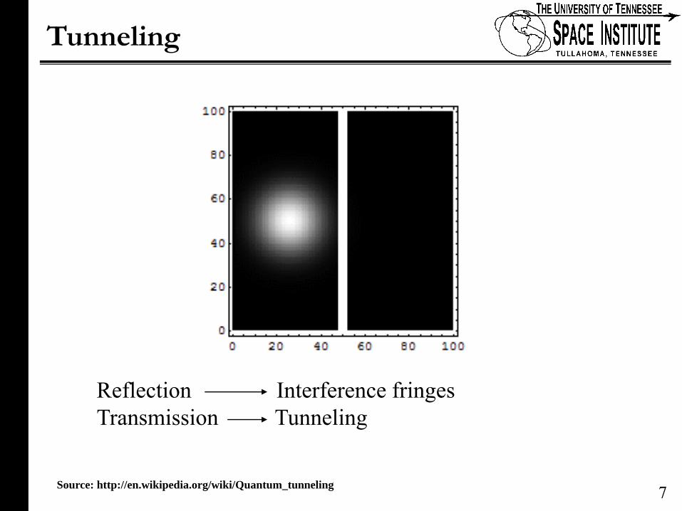
This transmission of the object through the potential hill is termed as tunneling.
Tunneling = Transmission through the potential barrier
In quantum mechanics, an electron can tunnel from theconduction into the valence band.
Such tunneling from an electron-like to hole-like state iscalled as interband tunneling or Klein tunneling.
Here, electron avoids backscattering
8
9 of xx
Tunneling in Graphene
In graphene, the massless carriers behave differently thanordinary massive carriers in the presence of an electricfield.
Here, electrons avoid backscattering because the carriervelocity is independent of the energy.
The absence of backscattering is responsible for the highconductivity in carbon nanotubes (Ando et al, 1998).
9
10 of xx
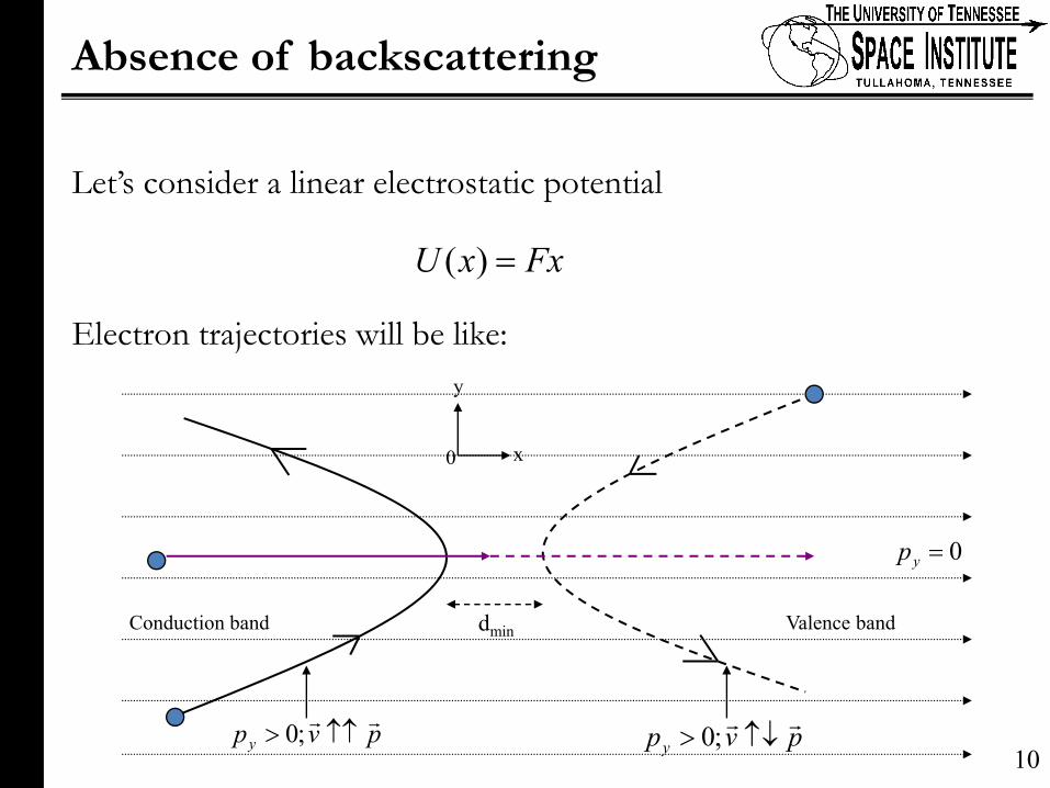
Absence of backscattering
Let’s consider a linear electrostatic potential
Electron trajectories will be like:
FxxU =)(
10
dmin
0 x
y
Conduction band Valence band
pvpyrr
↑↑> ;0 pvpyrr
↑↓> ;0
0=yp
11 of xx
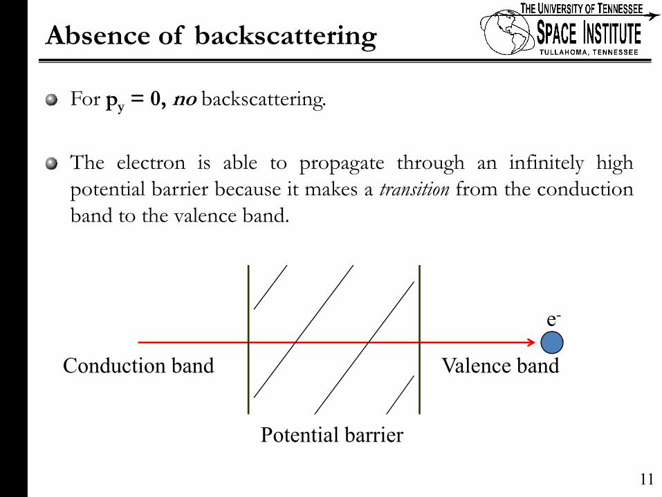
Absence of backscattering
For py = 0, no backscattering.
The electron is able to propagate through an infinitely highpotential barrier because it makes a transition from the conductionband to the valence band.
Conduction band Valence band
e-
Potential barrier
11
12 of xx
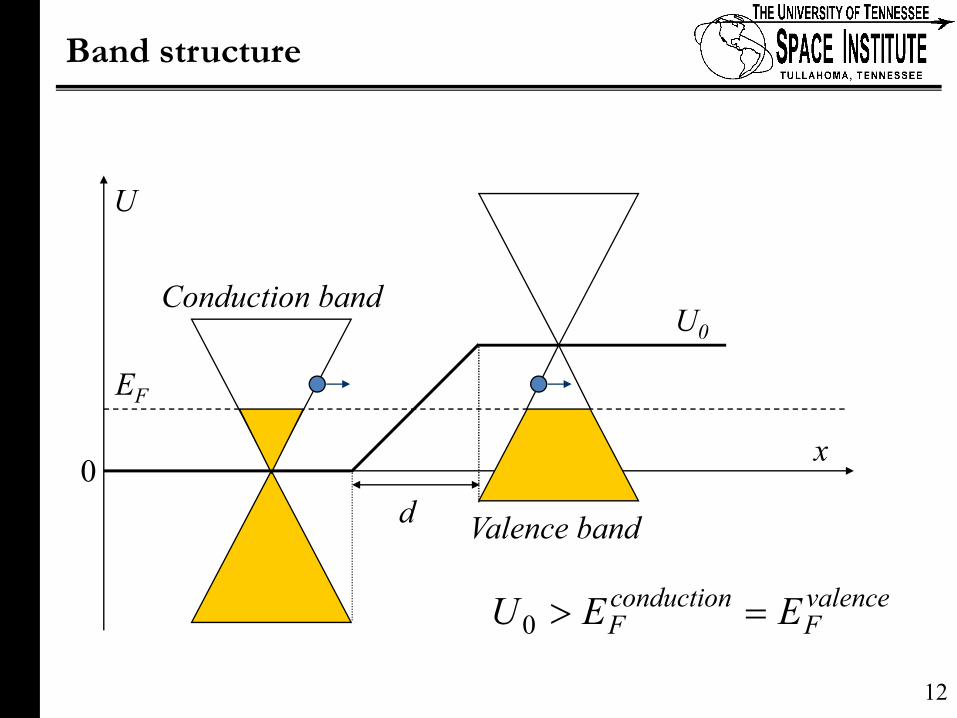
Band structure
d
U
EF
Conduction band
Valence band
U0
0x
valenceF
conductionF EEU =>0
12
13 of xx
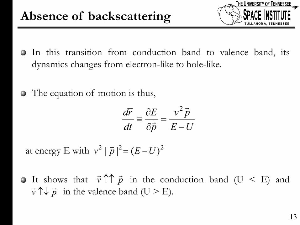
Absence of backscattering
In this transition from conduction band to valence band, itsdynamics changes from electron-like to hole-like.
The equation of motion is thus,
at energy E with
It shows that in the conduction band (U < E) andin the valence band (U > E).
UEpv
pE
dtrd
−=
∂∂
≡r
r
r 2
222 )(|| UEpv −=r
pvrr
↑↑pvrr
↑↓
13
14 of xx
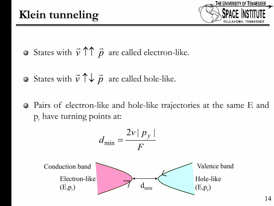
Klein tunneling
pvrr
↑↑States with are called electron-like.
States with are called hole-like.
Pairs of electron-like and hole-like trajectories at the same E andpy have turning points at:
pvrr
↑↓
Fpv
d y ||2min =
dmin
Electron-like(E,py)
Hole-like(E,py)
Conduction band Valence band
14
15 of xx
Klein tunneling
⎟⎟
⎠
⎞
⎜⎜
⎝
⎛ −=⎟⎟
⎠
⎞⎜⎜⎝
⎛ −=
Fvpdp
pT yyy
hh
2min exp
2||
exp)(ππ
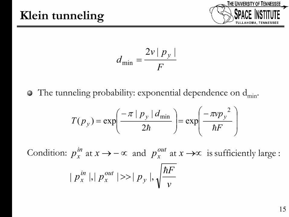
The tunneling probability: exponential dependence on dmin.
Fpv
d y ||2min =
vFppp
xpxp
youtx
inx
outx
inx
h |
:largely sufficient isat and at
|,||||, >>
→∝∝−→Condition:
15
16 of xx
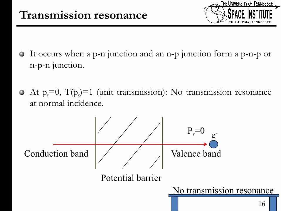
Transmission resonance
It occurs when a p-n junction and an n-p junction form a p-n-p orn-p-n junction.
At py=0, T(py)=1 (unit transmission): No transmission resonanceat normal incidence.
Conduction band Valence band
e-
Potential barrier
Py=0
No transmission resonance16
17 of xx
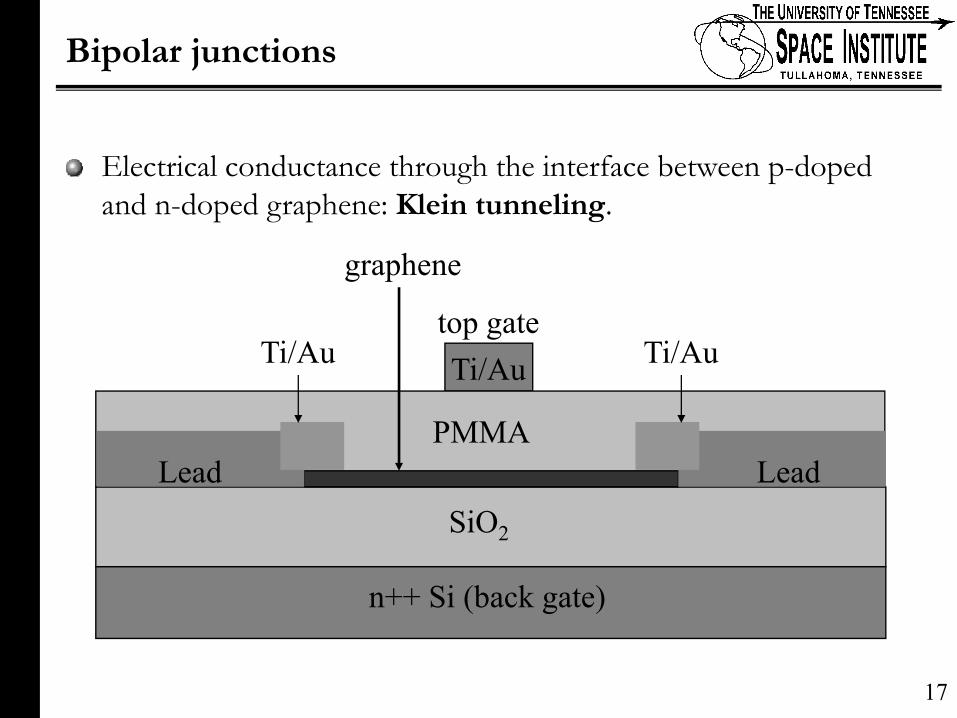
Bipolar junctions
Electrical conductance through the interface between p-doped and n-doped graphene: Klein tunneling.
n++ Si (back gate)
graphene
Ti/Au Ti/Au
Lead Lead
top gate
SiO2
PMMA
Ti/Au
17
18 of xx
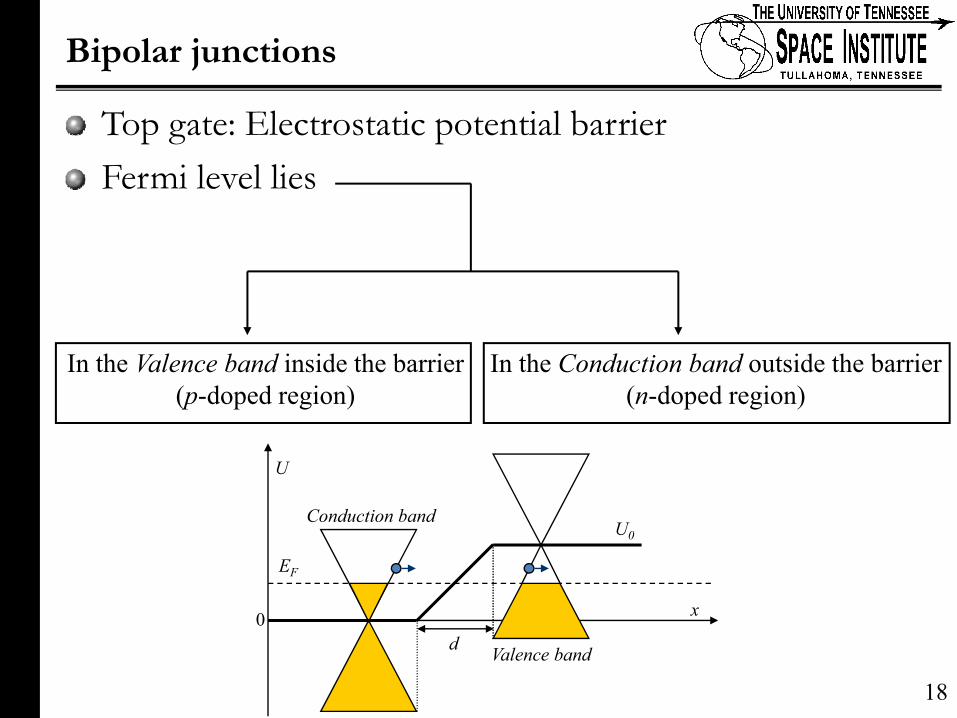
Bipolar junctions
Top gate: Electrostatic potential barrierFermi level lies
In the Valence band inside the barrier(p-doped region)
In the Conduction band outside the barrier(n-doped region)
d
U
EF
Conduction band
Valence band
U0
0 x
18
19 of xx
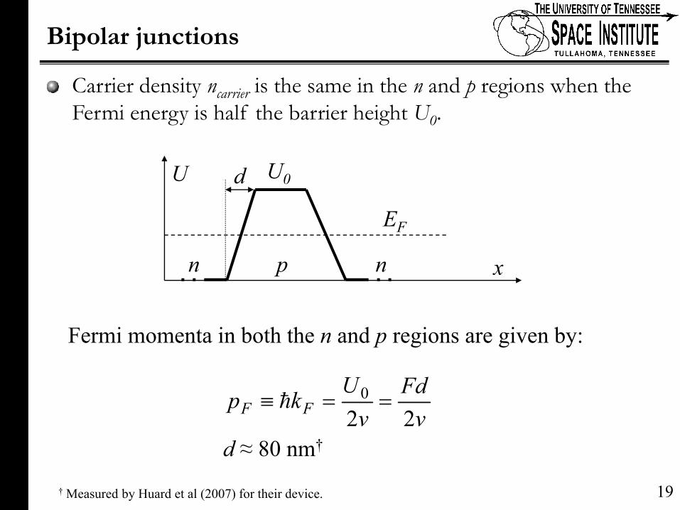
Bipolar junctions
Carrier density ncarrier is the same in the n and p regions when the Fermi energy is half the barrier height U0.
U0
EF
xn np
dU
Fermi momenta in both the n and p regions are given by:
vFd
vU
kp FF 220 ==≡ h
d ≈ 80 nm†
† Measured by Huard et al (2007) for their device. 19
20 of xx
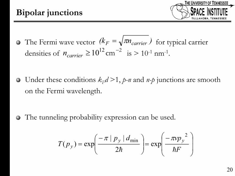
Bipolar junctions
The Fermi wave vector for typical carrier densities of is > 10-1 nm-1.
Under these conditions kFd >1, p-n and n-p junctions are smooth on the Fermi wavelength.
The tunneling probability expression can be used.
)n(k carrierF π=2cm−≥ 1210carriern
⎟⎟
⎠
⎞
⎜⎜
⎝
⎛ −=⎟⎟
⎠
⎞⎜⎜⎝
⎛ −=
Fvpdp
pT yyy
hh
2min exp
2||
exp)(ππ
20
21 of xx
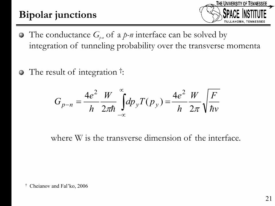
Bipolar junctions
The conductance Gp-n of a p-n interface can be solved by integration of tunneling probability over the transverse momenta
The result of integration †:
where W is the transverse dimension of the interface.
vFW
hepTdpW
heG yynp
hh ππ 24)(
24 22
∫∝
∝−
− ==
† Cheianov and Fal’ko, 2006
21
22 of xx
Applications of tunneling
Atomic clock
Scanning Tunneling Microscope
Tunneling diode
Tunneling transistor
22
23 of xx
Questions ?
Who got the Nobel prize (1973) in Physics for hispioneering work on electron tunneling in solids?