TU Ie technische universiteit eindhoven Faculty of Electrical Engineering Section Design Technology For Electronic Systems (ICS/ES) ICS-ES 841 Master's Thesis INTERFACING AN IP WITH PAUSIBLE CLOCKING. A case study for connecting IPto a Network on Chip. K.M.M. van Kaam Supervisor/Coach: Date: prof.dr.ir. J.L. van Meerbergen June 2004 The Faculty of Electrical Engineering of the Eindhoven University of Technology does not accept any responsibility regarding the contents of Master's Theses
Transcript
TUIe technische universiteit eindhoven
Faculty of Electrical EngineeringSection Design Technology For Electronic Systems (ICS/ES)
ICS-ES 841
Master's Thesis
INTERFACING AN IP WITH PAUSIBLE CLOCKING.A case study for connecting IPto a Network on Chip.
K.M.M. van Kaam
Supervisor/Coach:Date:
prof.dr.ir. J.L. van MeerbergenJune 2004
The Faculty of Electrical Engineering of the Eindhoven University of Technology does notaccept any responsibility regarding the contents of Master's Theses
Abstract: In nowadays digital IC designs multiple processors, memories and peripheralsare integrated and have become System on Chips (SoC). These SoCs typicallyhave multiple clock domains. As a result there is an increasing interest inGlobally Asynchronous Locally Synchronous (GALS) systems. The differentmodules in such a system are clocked locally and the communication between,modules is asynchronous. Therefore synchronization techniques must beapplied, which can be data or clock based. Furthermore due to the complexityof SoCs, the use of Networks on Chip (NoC) are also being proposed. NoCprovide a flexible communication architecture and guarantee of services. Theyalso reduce the need for long bus wiring.
Pausible clocking is a technique in which the clock generation is paused tosynchronize data. The goal is to connect modules that use pausible clocking tothe iEthereal Network on Chip. An obvious solution would be to use pausibleclocking for the NoC as well. However this causes a performance degradationof the network and the guarantee of services might be lost. A solution must befound that keeps the benefits of using a NoC and enables the usage of pausibleclocked modules interfaced to the iEthereal network.
The module that used pausible clocking is wrapped with an asynchronousshell consisting of a pausible clock generator and Input/Output controllers.Every I/O controller is interfaced to the pausible clock generator and to a .ripple-through FIFO that uses transition signalling. These FIFOs are alreadyused in the network as data queues. The asynchronous signals that arrive at theclock boundary of the network can be synchronized with data basedsynchronization techniques.
Signal Transition Graphs (STGs) are here used to formally proof the correctbehaviour of the pausible clock generator and to reason about its timing. TheVO controllers are defined with STGs, which can be synthesized to speedindependent Asynchronous Finite State Machines.
The pausible clock generator and the I/O controllers are implemented withstandard cells in. a 0.13 /.lm technology. A Mutual Exclusion element isdesigned as a standard cell, which is used in the pausible clock generator. Thedifferent asynchronous components are interfaced to make a simplecommunication channel, which is simulated with back-annotation from thelayout.
• Interfacing pausible clocked IP to a NoC without pausing the networkclock is proven (with STGs) to be feasible.
• In the pausible clocked IP module metastability can be prevented'during synchronization.
• The frequency of the pausible clock must be lower than the frequencyof the network.
• The clock is paused when the IP module writes data to a full FIFO orwhen it reads data from an empty FIFO. If the control sequence of anI/O controller takes longer than a clock cycle the clock is paused withevery write or read action.
• The data that is received by the IP module must be stored in an extralatch stage to keep, the data stable for sampling. An efficient solutionis adding a stage in the ripple-through FIFO for this purpose.
• To make the concept mature for products the concept must beincorporated in the design flow; possibilities for production testingmust be added and full-custom implementation of the I/O controllerscan be considered for better performance.
Asynchronous Finite State MachineApplication Specific Integrated CircuitBest EffortComputer Aided DesignClock Domain CrossingComplementary Metal Oxide SemiconductorComplete State CodingDigitally Controlled OscillatorDesign for TestDelay InsensitiveDevice Transaction LevelFirst In First OutFinite State MachineGlobally Asynchronous Locally Asynchronous .Globally Asynchronous Locally SynchronousGlobally Asynchronous Locally Dynamic SystemsGlobally SynchronousGuaranteed ThroughputHeader Parsing UnitIntegrated Circuitic front to backInput/OutputIslands of SynchronicityIntellectual PropertyInternational Technology Roadmap for SemiconductorsLocal SynchronousMutual Exclusion (element)Metal Oxide SemiconductorMean Time Between FailuresNetwork Interfacen-channel MOSNetwork on ChipPausible Clocking Controlp-channel MOSSoC Architecture and TechnologySynchronous BlockSystem on ChipSkeleton of ReUseSource SynchronousSignal Transition GraphsTuning for Best ExecutionVery Large Scale Integration
This Report is the result of the work during my graduation project, which has been carried outwithin the group Digital Design and Test at Philips Research in Eindhoven.
I would like to thank prof. dr. ir. J.L. van Meerbergen of the Eindhoven University ofTechnology, dr. K.G.W. Goossens and dr. ir. A.A. Abbo (both with Philips Research Eindhoven)for supervising my graduation project. Also I would like to thank ir. John Dielissen for hissupport and fruitful discussions about the Network Interface of the lEthereal Network on Chip.Furthermore I would like to thank ir. Paul Wielage for his discussions about asynchronous FIFOsand metastability issues and Dr. Francesco Pessolano for sharing his knowledge about SignalTransition Graphs. And of course I would like to thank all other colleagues not mentioned here,who supported me with my graduation.
The research carried out in the group Digital Design and Test (part of the IC design sector at thePhilips High-Tech Campus) aims to enable the integration of System on Chips (SoC) in state of 'the art and future CMOS technologies. MoSAIC, which stands for Methodology for SiliconArchitecting of ICs, aims improving the re-usability of IP modules and hence design productivityby means of a methodology that makes IP modules easier to integrate. An essential part of such amethodology is a flexible communication architecture. The goal of the iEthereal project [6][22] isto provide a Network on Chip (NoC) for this purpose. The graduation project described in thisreport is part of the MoSAIC and of the iEthereal projects.
1.1. Problem description
Figure 1.1 gives a schematic architecture of a SoC with several IP modules, which communicatevia such a iEthereal network. The network is composed of routers and every IP module isinterfaced to a router via a Network Interface (NI)..
Figure J. J: SoC with several IP modules and a /Ethereal networkfor on-chipcommunication
In a SoC as given in Figure 1.1 there typically exist multiple clock domains, which can becompletely independent. These multiple clock domains in a SoC can be caused by one or more ofthe following trends in IC design:
• In modern technology it is difficult to distribute a global high-speed low-skew clocksignal for the complete chip.
• IP modules can be firm cores that can not be changed and therefore the clock frequencyis predefined.
• IP modules might differ sensibly in clock frequency.
• The SoC uses dynamic frequency scaling for every IP module separately for dynamicpower management.
The emerging of SoC with multiple clock domains makes Globally Asynchronous LocallySynchronous (GALS) systems a viable and interesting design choice. In GALS systems every IPmodule keeps its own local clock domain and the communication between the different IPmodules is asynchronous. This communication is only possible when the necessarysynchronization between these clock domains is achieved. Several synchronization solutions areavailable, which could be applied to the architecture in Figure 1.1. All synchronization 'techniques are either clock based or data based. One clock based technique, which is calledpausible clocking is very interesting. The concept of synchronization by pausing the clock will beexplained in Paragraph 3.4. This synchronization technique has several advantages over moreconservative synchronization techniques:
• The chance of failure (Pr) due to metastability (see Paragraph 3.1) is zero, making thecomplete on-chip communication very robust. However non-determinism is introduced atsystem-level, which can cause problems for guarantees in the design.
• Asynchronous handshaking is used for data communication between IP modules, whichhave their own local (independent) clock domain. If frequencies are not predictable (e.g.if dynamic frequency scaling is used) the communication remains robust.
• Pausible clocking can be added to a Locally Synchronous (LS) module as a shell, makingintegration of soft cores as well as firm cores possible.
• Pausible clocking simplifies the use of dynamic frequency scaling.
For the architecture in Figure 1.1 the network must have a common clock frequency, because theiEthereal network uses time-division-multiplex circuit-switching, which can provide guaranteedservices. All IP modules can have an independent pausible clock domain. However the networkcan not use pausible clocking, because the global communication of the SoC is stopped when thenetwork clock is paused for synchronization with a certain IP module. This will result in aperformance degradation of the network, and the guarantee of services is lost.
Thus the question (or problem) is how to connect the Network Interface of the iEthereal networkto an IP module, when this IP module uses pausible clocking for synchronization and the clock ofthe network can not be paused. When a solution is found further questions are what theconsequences are for a SoC and how this solution can be implemented.
1.2. Contents
After this general introduction the following two Chapters give more background information.Chapter 2 first gives background information about asynchronous design. The two main topics inthis Chapter are Signal Transition Graphs and asynchronous components, which are used for theimplementation. Chapter 3 gives background information about synchronization in general. Athorough explanation of metastability is given, and synchronization techniques using pausibleclocking or dual flip-flop synchronizers are described.
In Chapter 4 the Network Interface (NI) of the iEthereal network is introduced. The ripplethrough FIFOs, which are used in this NI are described in here as well. A top-level architecturefor interfacing an IP module with a pausible clock domain to the Network Interface that has anon-pausible clock domain is introduced. The synchronizers that are necessary for this top-levelarchitecture are also discussed in Chapter 4. In the following Chapters the components of thisarchitecture are described.
Chapter 5 introduces a pausible clock generator. The timing of the basic circuit of the pausibleclock generator is described and a solution for interfacing multiple VO controllers to the pausibleclock generator is given. Chapter 6 and Chapter 7 describe solutions for the output and inputcontrollers respectively. The interfacing, the behaviour and the timing specification of these VOcontrollers are described. The behaviour of the I/O controllers is specified with Signal TransitionGraphs, which can be mapped to Asynchronous Finite State Machines. Chapter 8 gives the 'implementation of a Mutual Exclusion element, the pausible clock generator and the I/Ocontrollersin a CMOS12 process. The report ends with conclusions in Chapter 9.
1.2.1. For the reader
Throughout this report signal names and special names for components are given in italics. Forexample when the signal with the name "accept" is used in a sentence it is written as: accept.
When Boolean functions are used throughout this report then the following syntax for thesefunctions is used:
• Negation (NOT): the variable that is negated has an apostrophe behind its variable name(e.g. var').
• AND: there is no special character or an asterisk (*) between variables (e.g. varl var2).
• OR: there is a plus sign between variables (e.g. varl + var2).
The next Figures give the meaning of the symbols of the logic gates and sequential elements thatare used in the schematics in this report.
Input port
~
Output port
-----IZEEE>
Figure 1.2: input port (left) and output port (right)
I--{>---{>-IFigure 1.3: inverter (left) and buffer (right)
Figure 1.4: OR gate (left) and NOR gate (right)
D-XOR
D-XNOR
Figure 1.5: Exclusive OR gate (left) and Exclusive NOR gate (right)
Figure 1. 6: AND gate (left) and NAND gate (right)
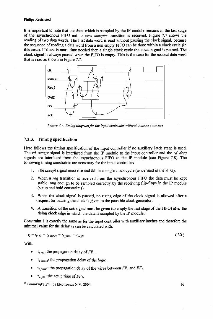
Figure 1.7: Muller C-element (left) and Muller C-element with inverted output (right)
I -{............I __.:..L<'------}- I
Figure 1.8: delay-line with delay T)
Figure 1.9: latch with enable signal and data input and output
o SET Q
elk"",Q
clear
14
Figure 1.10: D flip-flop with clock input(clk), data input (D) and data ouput (Q); optionalare the inverted data output (Q') and the asynchronous reset (clear)
This chapter gives a brief summary of asynchronous design techniques, asynchronouscomponents and asynchronous circuit modelling with Signal Transition Graphs (STGs) that are 'used later on in this report. An overview of different asynchronous design techniques is given in[28] and [9].
Asynchronous design does not use a clock signal as is used in synchronous design. This gives anumber of advantages of which the most important advantages are given below:
• Lower power consumption: in synchronous design every memory element switches everyclock cycle, thus also when the data is not changed. In asynchronous design the memoryelement only switches when new data is received.
• Less emission of electro-magnetic noise: the switching of the logic and memory elementsof asynchronous designs is more spread out than in synchronous designs.
• No clock distribution and clock skew problems, because there is no global clock signal.
• High operation speed: the operation speed is determined by the delays in the circuit. Thisis the same as in synchronous design, however in synchronous design the longest path (orthe longest delay) determines the maximum clock frequency and with this the speed. Inasynchronous design every delay is local, which means that there is never more timeused then the delay of the local path itself.
Despite these advantages, asynchronous design is normally adapted. The main reason is that theavailable tools for making asynchronous systems is limited.
2.1. Handshaking
To pass data in an asynchronous system, handshaking is used. Different protocols exist, but hereonly the bundled-data protocol is discussed. The bundled-data protocol refers to a situation wherethe data signals use normal Boolean levels to encode information. Bundled-data protocols need asingle request signal (Req) and a single acknowledge signal (Ack). These two signals are bundledwith a number of data signals. When data is send there is always an initiator and a target andthere is a sender and a receiver. When the initiator is the sender and the target is the receiver thechannel is called a push channel. When the initiator is the receiver and the target is the sender thechannel is called a pull channel. Both channels are shown in Figure 2.1, a black dot indicates theinitiator.
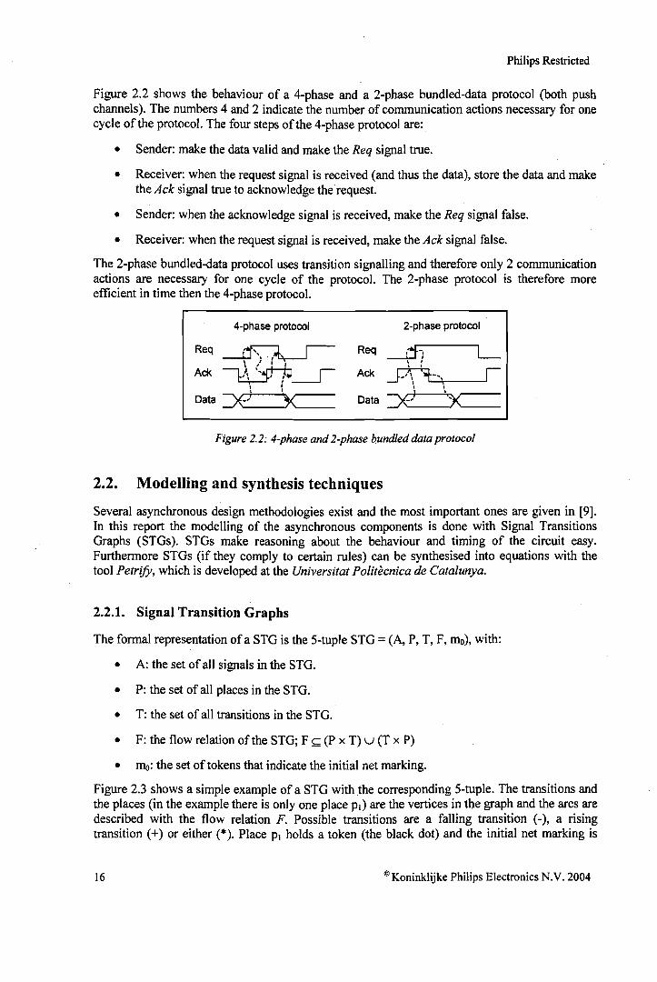
Figure 2.2 shows the behaviour of a 4-phase and a 2-phase bundled-data protocol (both pushchannels). The numbers 4 and 2 indicate the number of communication actions necessary for onecycle of the protocol. The four steps ofthe 4-phase protocol are:
• Sender: make the data valid and make the Req signal true.
• Receiver: when the request signal is received (and thus the data), store the data and makethe Ack signal true to acknowledge therequest.
• Sender: when the acknowledge signal is received, make the Req signal false.
• Receiver: when the request signal is received, make the Ack signal false.
The 2-phase bundled-data protocol uses transition signalling and therefore only 2 communicationactions are necessary for one cycle of the protocol. The 2-phase protocol is therefore moreefficient in time then the 4-phase protocol.
4-phase protocol
Req .~ r--
~----r)I:~
Ack ~ '.'\ ':
I II I
Data J(-- '<,-__
2-phase protocol
Figure 2.2: 4-phase and 2-phase bundled data protocol
2.2. Modelling and synthesis techniques
Several asynchronous design methodologies exist and the most important ones are given in [9].In this report the modelling of the asynchronous components is done with Signal TransitionsGraphs (STGs). STGs make reasoning about the behaviour and timing of the circuit easy.Furthermore STGs (if they comply to certain rules) can be synthesised into equations with thetool Petrify, which is developed at the Universitat Politecnica de Catalunya.
2.2.1. Signal Transition Graphs
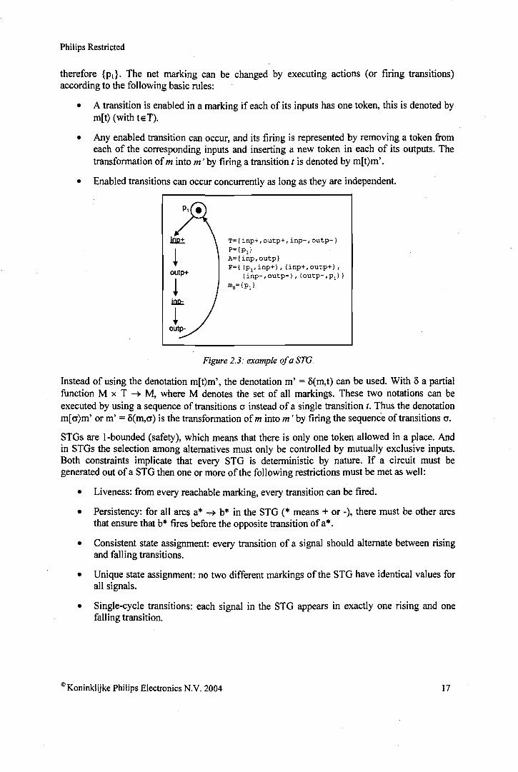
The formal representation of a STG is the 5-tuple STG =(A, P, T, F, mo), with:
• A: the set of all signals in the STG.
• P: the set of all places in the STG.
• T: the set of all transitions in the STG.
• F: the flow relation ofthe STG; F ~ (P x T) u (T x P)
• rno: the set of tokens that indicate the initial net marking.
Figure 2.3 shows a simple example of a STG with the corresponding 5-tuple. The transitions andthe places (in the example there is only one place PI) are the vertices in tbe graph and the arcs aredescribed with the flow relation F. Possible transitions are a falling transition (-), a risingtransition (+) or either (*). Place PI holds a token (the black dot) and the initial net marking is
therefore {PI}' The net marking can be changed by executing actions (or firing transitions)according to the following basic rules:
• A transition is enabled in a marking if each of its inputs has one token, this is denoted bym[t) (with teT).
• Any enabled transition can occur, and its firing is represented by removing a token fromeach of the corresponding inputs and inserting a new token in each of its outputs. Thetransformation ofminto m' by firing a transition t is denoted by m[t)m'.
• Enabled transitions can occur concurrently as long as they are independent.
Instead of using the denotation m[t)m', the denotation m' = o(m,t) can be used. With 0 a partialfunction M x T ~ M, where M denotes the set of all markings. These two notations can beexecuted by using a sequence of transitions cr instead of a single transition t. Thus the denotationm[cr)m' or m' = o(m,cr) is the transformation ofm into m' by firing the sequence of transitions cr.
SrGs are I-bounded (safety), which means that there is only one token allowed in a place. Andin STGs the selection among alternatives must only be controlled by mutually exclusive inputs.Both constraints implicate that every STG is deterministic by nature. If a circuit must begenerated out ofa STG then one or more ofthe following restrictions must be met as well:
• Liveness: from every reachable marking, every transition can be fired.
• Persistency: for all arcs a* ~ b* in the STG (* means + or .), there must be other arcsthat ensure that b* fires before the opposite transition of a*.
• Consistent state assignment: every transition of a signal should alternate between risingand falling transitions.
• Unique state assignment: no two different markings of the STG have identical values forall signals.
• Single-cycle transitions: each signal in the STG appears in exactly one rising and onefalling transition.
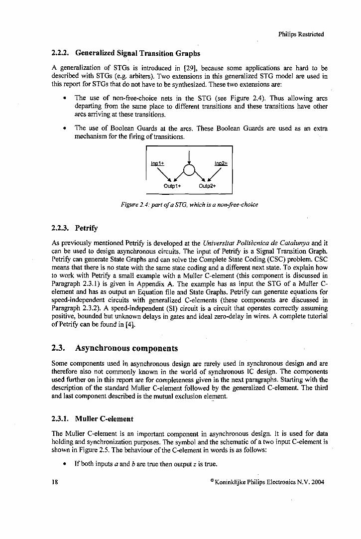
A generalization of STGs is introduced in [29], because some applications are hard to bedescribed with STGs (e.g. arbiters). Two extensions in this generalized STG model are used inthis report for STGs that do not have to be synthesized. These two extensions are:
• The use of non-free-choice nets in the STG (see Figure 2.4). Thus allowing arcsdeparting from the same place to different transitions and these transitions have otherarcs arriving at these transitions.
• The use of Boolean Guards at the arcs. These Boolean Guards are used as an extramechanism for the firing of transitions.
Outp1+ Outp2+
Figure 2.4: part ofa STG, which is a non-free-choice
2.2.3. Petrify
As previously mentioned Petrify is developed at the Universitat Politecnica de Catalunya and itcan be used to design asynchronous circuits. The input of Petrify is a Signal Transition Graph.Petrify can generate State Graphs and can solve the Complete State Coding (CSC) problem. CSCmeans that there is no state with the same state coding and a different next state. To explain howto work with Petrify a small example with a Muller C-element (this component is discussed inParagraph 2.3.1) is given in Appendix A. The example has as input the STG of a Muller Celement and has as output an Equation file and State Graphs. Petrify can generate equations forspeed-independent circuits with generalized C-elements (these components are discussed inParagraph 2.3.2). A speed-independent (SI) circuit is a circuit that operates correctly assumingpositive, bounded but unknown delays in gates and ideal zero-delay in wires. A complete tutorialof Petrify can be found in [4].
2.3. Asynchronous components
Some components used in asynchronous design are rarely used in synchronous design and aretherefore also not commonly known in the world of synchronous IC design. The componentsused further on in this report are for completeness given in the next paragraphs. Starting with thedescription of the standard Muller C-element followed by the generalized C-element. The thirdand last component described is the mutual exclusion element.
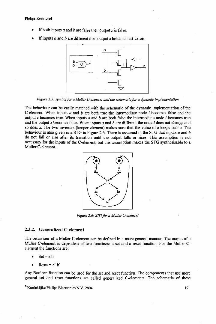
2.3.1. Muller C-element
The Muller C-element is an important component in asynchronous design. It is used for dataholding and synchronization purposes. The symbol and the schematic of a two input C-element isshown in Figure 2.5. The behaviour ofthe C-element in words is as follows:
• If both inputs a and b are true then output z is true.
• If both inputs a and b are false then output z is false.
• If inputs a and b are different thenoutput z holds its last value.
a
bz
Figure 2.5: symbolfor a Muller C-element and the schematicfor a dynamic implementation
The behaviour can be easily matched with the schematic of the dynamic implementation of theC-element. When inputs a and b are both true the intermediate node i becomes false and theoutput z becomes true. When inputs a and b are both false the intermediate node i becomes trueand the output z becomes false. When inputs a and b are different the node i does not change andso does z. The two inverters (keeper element) makes sure that the value of z keeps stable. Thebehaviour is also given in a STG in Figure 2.6. There is assumed in the STG that inputs a and bdo not fall or rise after its transition until the output falls or rises. This assumption is notnecessary for the inputs of the C-element, but this assumption makes the STG synthesisable to aMuller C-element.
Figure 2.6: srG for a Muller C-element
2.3.2. Generalized C-element
The behaviour of a Muller C-element can be defined in a more general manner. The output of aMuller C-element is dependent of two functions: a set and a reset function. For the Muller Celement the functions are:
• Set =a b
• Reset = a' b'
Any Boolean function can be used for the set and reset function. The components that use moregeneral set and reset functions are called generalized C-elements. The schematic of these
elements with an example are shown in Figure 2.7. In the example the output z becomes true ifinputs a and b are true. The output z becomes false if inputs band c are false. Of course the setand the reset function are not allowed to be true for the same input values, because otherwisethere will be a short circuit between the power supply and the ground. The operation ofthe circuitof generalized C-elements is similar to the Muller C-element.
set{z) =abreset{z) =b'c'
Cc----4
b
b~z z
ba 8-----1
Figure 2.7: the common circuit and an example ofa generalized C-element
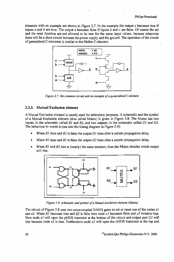
2.3.3. Mutual Exclusion element
A Mutual Exclusion element is mostly used for arbitration purposes. A schematic and the symbolof a Mutual Exclusion element (also called Mutex) is given in Figure 2.8. The Mutex has twoinputs, in the schematic called Rl and R2, and two outputs, in the schematic called Gl and G2.The behaviour in words is (see also the timing diagram in Figure 2.9):
• When Rl rises and R2 is false the output G1 rises after a certain propagation delay.
• When R2 rises and Rl is false the output G2 rises after a certain propagation delay.
• When Rl and R2 rise at (nearly) the same moment, then the Mutex decides which outputwill rise.
Figure 2.8: schematic and symbol ofa Mutual Exclusion element (Mutex)
The circuit of Figure 2.8 uses two cross-coupled NAND gates to set or reset one of the nodes xland x2. When Rl becomes true and R2 is false then node xl becomes false and x2 remains true.Now node xl will open the pMOS transistor at the bottom of the circuit and output port Gl willrise because node x2 is true. Furthermore node x2 will open the nMOS transistor at the top and
will pull output G2 to the ground, thus G2 is false. The inverse behaviour happens when R2becomes true and Rl is false.
When input Rl and R2 rise at (nearly) the same moment in time then there will occurmetastability (see Paragraph 3.1) at the outputs of the cross-coupled NAND gates. Whenmetastability occurs the nodes xl and x2 will have an undefined value, typically the voltage of .the nodes will be half of the supply voltage. To prevent that the outputs of the Mutex also haveundefined values the 4 transistors "filter" out the undefined values ofxl and x2. The metastabilitywill end when the voltage difference of the nodes xl and x2 reaches the thresholds of thetransistors in the filter circuit. When this happens depends on the noise in the circuit and thearrival times of the input signals Rl and R2.
To illustrate the behaviour of the Mutex somewhat further, the (generalized) STG for a Mutex isgiven in Figure 2.10. The STG uses a non-free choice net forthe place in the middle of the STG.The token in this place will be "stolen" by transition Rl + or R2+, dependent on which transitionsfires first. For example if R1+ fires, the token of the place in the middle is taken. Next if nowtransition R2+ fires then the transition G2+ can only fire when the token is put back in the placein the middle (when transition Gl- has fired). The token is taken again when transition G2+ fires.
This chapter first gives a thorough description of metastability. In synchronous designmetastability is prevented by using worst case timing constraints on the design. Furthermore'static timing analysis is applied when the design is finished and if problems are reported theseshould be fixed in the design. Synchronizers can be used to synchronize asynchronous signals,which are received in a synchronous design. A single flip-flop can be used as a synchronizer, butas is described in this Chapter a single flip-flop is not sufficient for a robust synchronization.When asynchronous signals must be sampled by synchronizers, such that the sampled signals canbe used in a synchronous design, metastability can occur in these synchronizers. If this happensthere is a chance that the device malfunctions.
A classification of signal to clock synchronization is given along with a matrix that gives thedifferent clock generation techniques versus different synchronization techniques. Two importantsynchronization techniques are described in this chapter: synchronization with pausible clockingand the usage of dual flip-flop synchronizers.
3.1. Metastability
Basically if a sequential gate with a data and a sampling input has a transition on both theseinputs at the same time, metastability occurs. "At the same time" is not really a good definition.The time window in which metastability occurs (Metastability Window: Tw) is a characteristic ofthe design of the sequential gate. When metastability occurs the sequential gate may remain in anin-between state, called the "metastable state", for an indeterminate time interval. Eventually, theoutput of the sequential element settles to a logical zero or a logical one. While it is settling, itsoutput may glitch, oscillate, sit at an intermediate voltage, or merely show an increased clock-tooutput delay. The time needed to resolve from the metastable state 'is called 't (Resolve TimeConstant) and this constant is a characteristic of the implementation. The constants Tw and 't aredifficult to determine, the best way is by doing measurements on the sequential gate itself anddetermine the statistical properties [7]. Another approach is by doing simulations of thesequential gate, but this is less accurate. Figure 3. I shows a simulation of two cross-coupledNAND gates in a 0.13 Ilm process technology (CMOS12) forming a Set/Reset latch (this circuitis already discussed in Paragraph 2.3.3 for the Mutual Exclusion element).
Both data inputs (the Set and Reset) get a rising transition close to each other. It shows that thecloser the transitions are the longer it takes to get a logical one or a logical zero at the output.
The probability of a metastable event lasting longer than some time, t, is defined as:
-t/P=e lT ( 1 )
3.1.1. Finding Twand rfor a flip-flop
A D-flip-flop with asynchronous reset from the CMOS12 standard cell library (type dj2sqx05) isused to find the values for Tw and T for this flip-flop. To find the values the Pstar simulator isused on the netlist of this flip-flop with all parasitic components (abstracted netlist of the layoutof the flip-flop). During the simulation the data arrival time is swept around the setup timeinterval. Figure 3.2 shows a simulation result for some different input data signals. The datasignals with delay values -80 ps, -68 ps and -66 ps are still early enough to be clocked into theflip-flop, the others are to late and do not change the output Q. The data signals that can changethe output introduce a larger propagation delay, which is caused by the metastability occurring inthe first latch stage ofthe flip-flop.
Output first D~~>--- ---~D3latch stage ---~>--- ._--
The used flip-flop has a load of only 6 fF in the simulation, which makes the propagation delayof the flip-flop as small as possible. The propagation delay for the data to output transition for alow to high transition found in the datasheet is 171 ps. Furthermore the setup time of the flip-flopfor a logic one at the data input is 72.1 ps, which matches with the simulation results shown inFigure 3.2.
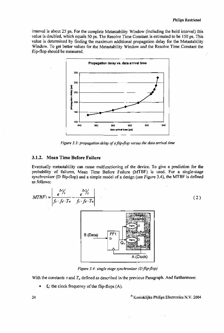
The different arrival times of the data are plotted versus the propagation delay of the flip-flop inFigure 3.3. The plot is only made for the setup interval and not for the hold interval. The holdinterval looks the same as the setup interval, but it is flipped vertically [7]. Now an estimate ofthe Metastability Window Tw and the Resolve Time Constant T can be made. The normalpropagation time of the flip-flop should be about 171 ps. Take the maximum propagation timewithout metastability to happen to be 200 ps, then the Metastability Window for the setup
interval is about 25 ps. For the complete Metastability Window (including the hold interval) thisvalue is doubled, which equals 50 ps. The Resolve Time Constant is estimated to be 150 ps. Thisvalue is determined by finding the maximum additional propagation delay for the MetastabilityWindow. To get better values for the Metastability Window and the Resolve Time Constant theflip-flop should be measured.
Figure 3.3: propagation delay ofaflip-jlop versus the data arrival time
3.1.2. Mean Time Before Failure
Eventually metastability can cause malfunctioning of the device. To give a prediction for theprobability of failures, Mean Time Before Failure (MTBF) is used. For a single-stagesynchronizer (D flip-flop) and a simple model of a design (see Figure 3.4), the MTBF is definedas follows:
trIl tr2/e h e h
MI'BFI =1---fc . jd .Tw fc .fd .Tw
(2)
B (Data) FF1D
A (Clock)
Figure 3.4: single stage synchronizer (D flip-jlop)
With the constants rand Tw defined as described in the previous Paragraph. And furthermore:
• 41: the time available for metastability to be resolved for logicJ.
• 42: the time available for metastability to be resolved for logic2'
This formula calculates the number of faults that can happen due to data inconsistency in thesampled values after logic, and logic). For example if metastability does not propagate throughlogic), but it propagates through logic, there is an inconsistency between the two data valuessampled by the flip-flops in the receiver.
The variables 1r, and 1r2 are dependent of a number of timing parameters. First of all the clockfrequency ofthe flip-flop determines the maximum time available before new data is clocked intothe next flip.;.flop. This maximum time is reduced by the setup time of the flip-flop in thereceiver, the propagation delay of the flip-flop FF" the propagation delay of the wires and thepropagation delay of the logic between two flip-flop stages. Thus the formulas for the resolvingtime tr, and 1r2 are:
• tsetup: the setup time of the flip-flops in the receiver.
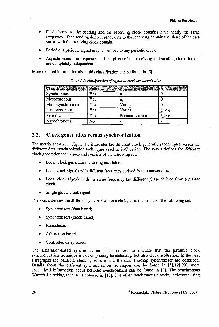
3.2. Classification of signal to clock synchronization
(3 )
(4)
The different signal-to-clock synchronizations can be classified according to the characteristics ofthe phase and frequency dependencies. These dependencies are given in Table 3.1 and thedescriptions of the different types ofsignal-to-clock synchronization are given below:
• Synchronous: data is sampled at the same frequency and with the same phase for thesending and receiving clock domain. (Typically the sending and the receiving clockdomain are the same clock domain.)
• Mesochronous: data is sampled at the same frequency, but the clock phase between thesending and receiving clock domains has a constant phase difference.
• Multi-synchronous: the same as mesochronous, but the phase differences is variable.
• Plesiochronous: the sending and the receiving clock domains have nearly the samefrequency. If the sending domain sends data to the receiving domain the phase ofthe datavaries with the receiving clock domain.
• Periodic: a periodic signal is synchronized to any periodic clock.
• Asynchronous: the frequency and the phase of the receiving and sending clock domainare completely independent.
More detailed information about this classification can be found in [5].
Table 3. J: classification ofsignal to clock synchronisation
S nchronousMesochronousMulti-s nchronousPlesiochronousPeriodicAs nchronous
VariesVariesPeriodic variation
ooo
3.3. Clock generation versus synchronization
The matrix shown in Figure 3.5 illustrates the different clock generation techniques versus thedifferent data synchronization techniques used in SoC design. The y-axis defines the differentclock generation techniques and consists of the following set:
• Local clock generation with ring oscillators.
• Local clock signals with different frequency derived from a master clock.
• Local clock signals with the same frequency but different phase derived from a masterclock.
• Single global clock signal.
The x-axis defines the different synchronization techniques and consistsofthe following set:
• Synchronizers (data based).
• Synchronizers (clock based).
• Handshake.
• Arbitration based.
• Controlled delay based.
The arbitration-based synchronization is introduced to indicate that the pausible clocksynchronization technique is not only using handshaking, but also clock arbitration. In the nextParagraphs the pausible clocking scheme and the dual flip-flop synchronizer are described.Details about the different synchronization techniques can be found in [5][19][20], morespecialized information about periodic synchronizers can be found in [9]. The synchronousWaterfall clocking scheme is covered in [12]. The other synchronous clocking schemes: using
HIX clock trees, using PLLs and using DLLs are standard approaches for distributing a globalclock signal in the design.
GALS
LocaldOck generation I Dual flip-flop d! iIPausible docking schemewith ring oscillators : : :______:_n ~ n_. +_+-----------------~------------- _Local dock signals with IDual flip-flop di :ICDC FIFO d:different frequency . : : :
=~fro~,~~ster i II ~~~~~~~; I!I !I ~!______________________ ... _ ~ ... .. L _
Local dock signals with _',;_:,: !the same frequenc;ybut different phase _i .! !deriVedfrom·-a-master : : :clock.'·· ...···'.. :::~
F--:::--::;--:=:--=-=·~:::--::;--:=:--=--=-:::--::;--:=:--=-a__----_+:;;;;:;;::iffi!::i~!5iiiii':~---~!;---~~Single global dock : ,1_, i_~~~t~twithaXTAL ! i_I 0 i
'-- --_.....ot I I I I
-------------:..-------------j------------------i-----------.-------t-----------------t--..-------------+----------------[II Synchronous 11 Synchronizers Iii Synchronizers 1: 1Handshake I!I Arbitration Iii Controlled I
iI (Data based) !I (Clock based) !I IiI based il delay basedIII Mesochronous 0 , 0 , 0'-- --'
• Periodic (streaming)
Cd Asynchronous
Figure 3.5: clock generation versus synchronization techniques
3.4. Pausible clocking in GALS systems
The concept of Globally Asynchronous Locally Synchronous (GALS) is introduced by Chapiro[3], but the usage ofpausible clocking for systems is first introduced by Yun [34][35]. The usageof pausible clocking in GALS evolved further and Borman [1] introduced an asynchronouswrapper for pausible clocking to be used in GALS systems. Although the concept of pausibleclocking seems to be very promising, the usage in real products is limited. Muttersbach et. al.implemented pausible clocking in several designs [16][17][32]. An overview of different GALSsystems and the universities, research institutes and companies that work on GALS systems withpausible clocking can be found in [12].
In general the approach for GALS systems with pausible clocking is wrapping a LocalSynchronous (LS) module with asynchronous components including the pausible clock generator(see Figure 3.6). The LS module is then first designed in a standard synchronous manner. Apausible clock generator is added for every Local Synchronous (LS) module, which can pause theclock signal for synchronizing data, which is exchanged with another LS module. The controllersthat control the data transfer are asynchronous and use handshaking between different LSmodules (every type of handshaking can be used). The implementation of the I/O controllers andthe pausible clock generator can' be done in several manners, dependent of the chosenasynchronous design techniques and handshaking techniques. A thorough description about thebehaviour and timing of a pausible clock generator is given in Chapter 5.
Next an example of communicating data in a push channel with using 4-phase handshaking (withbundled data) is described.
When a LS module wants to send data (the initiator) to another LS module (the target), theinitiator requests to send data to its asynchronous output controller. Then the output controllerrequests to pause the generation of the clock signal and sends a request signal to the target. Thisrequest signal is received by the target at the input controller and this controller requests to pausethe generation of the clock signal of the target. This is acknowledged back to the initiator and theinitiator sends the data and an acknowledgement of this action. When this acknowledgement is 'received by the target the clock generation of the target can be started again and the data issampled. An acknowledge signal is send back to the initiator, which can then safely start theclock generation again.
Figure 3.6: asynchronous wrapperfor GALS systems with the usage ofpausibleclocldng
3.5. Dual flip-flop synchronizer
For a single flip-flop synchronizer the formula for the MTBF was presented in Paragraph 3.1.2.With the values found for the Metastability Window (50 ps) and the Resolve Time Constant (150ps) the MTBF can be calculated for different values of the clock frequency of the receiver. Afixed data event frequency of 10 Mhz is taken and the setup time of the flip-flop used is 70 ps.The simple model for the design is taken as shown in Figure 304. The delay through logic I
(including wires) is taken as 50% of the clock cycle and the delay through logic] (includingwires) is taken as 60% of the clock cycle. Furthermore there is assumed that the data input signalis asynchronous, thus this signal has no relation with the clock signal of the receiver and is notperiodic either. The resulting MTBF values for these parameters and the simple model of thedesign are given in Table 3.2. With increasing clock frequencies the MTBF gets worse, forexample at 200 MHz clock frequency a failure happens every 29 seconds. For the 500 MHz clockfrequency there are about 2000 failures every second.
Table 3.2: MTBFvaluesfor a singlejUp-jlop synchronizer (dflsqx05)
Obviously a single flip-flop cannot be used as a synchronizer between two independent clockdomains. Therefore a dual flip-flop synchronizer is normally used in multiple clock systems, seeFigure 3.7. Two disadvantages of this synchronizer are:
• There is still a chance ofmetastability.
• An additional latency for synchronization is paid.
B (Data)--+I
A (Clock)
Figure 3.7: dual flip-flop synchronizer
The chance of metastability can be reduced further by using more flip-flops in serial, but ofexpense of latency. There is always a trade-off between robustness and the latency of thesynchronizer. Sometimes the design of the dual flip-flop is altered by designers to decrease thelatency, but this has a negative effect on the robustness of the synchronizer (the chance ofmetastability is increased). An example ofthis is given in [10].
3.5.1. MTBF for dual flip-flop synchronizers
The MTBF for a dual flip-flop synchronizer and the simple model of a design (see Figure 3.7) isdefined similar as for a single flip-flop synchronizer:
trl/ tr2/e IT e h
MI'BF=I---/c. jJI' Tw /c. j12-Tw
( 5 )
However the parameterstil and fd2 are not known in advance, but it is assumed that they give theprobability that the first flip-flop has not settled by one setup time before the clock of the secondflip-flop. This means thatfdf,ft12, trf and tr2can be rewritten to:
Now the resulting formula for the MTBF of a dual flip-flop synchronizer can be derived:
e (9)tr logie2
etr _Iogicl
e r-:----.....,....---1 =1-----
[ Jjd . f/ .Tw 2;:L;;, .J·T.
With tr_logicl and t r_logie2 defined as:
2tr log icl =- - 2 . tsetup .ff - Ip .ff - Ip wirel - Ip logicl-fc - - - - ( 10)
2tr log ie2 =- - 2 . tsetup .ff - Ip .ff - Ip wir.2 - Ip loaie2- fc - - - - ~.
( 11 )
This method can be repeated for every depth (number of flip-flops in serial) of the synchronizer.In general if the synchronizer has N flip-flops in serial, the MTBF can be formulated as:
Ir 10gicl(N)
etr logie2(N)
( 12)
With:
N Ntr _log icl(N) = -;: - tp _.ff - t p _ wirel - tp _Iogicl - ~)setUP_ i
JC ~
( I3 )
(14 )
By increasing the number of flip-flop stages in the synchronizer the MTBF increases, but also thearea and the latency of the synchronizer increases. The MTBF for different clock frequencies forthe dual flip-flop synchronizer is given in Table 3.3. The values are calculated with the sameparameter values as for the single flip-flop synchronizer. Remember that the calculated values forthe MTBF are just an indication, because the values for the Metastability Window and theResolve Time Constant are estimates and a simple model of a design taken.
Compared to the single flip-flop synchronizer the MTBF of the dual flip-flop synchronizer isimproved quite a lot, but if the receiving clock domain is 500 Mhz or larger the MTBF is notgood enough anymore. Then more flip-flop stages are necessary which makes the silicon areaand the latency for synchronization larger.
Figure 3.8 gives the trend of the MTBF (vertical axis) versus the clock frequency (horizontalaxis) of the receiver for different synchronizers. The synchronizers differ in the number of flipflops used in serial: mtbfl uses a single flip-flop, mtbj2 uses two flip-flops, etc... The Figureshows indeed that a synchronizer with more flip-flops in serial has a better MTBF. Also theMTBF decreases enormously when the clock frequency of the receiver is increases.
This chapter introduces the top-level architecture for interfacing the Network Interface (NI) to IPmodules that use pausible clocking for synchronization. First a short introduction of the NI of '}Ethereal is given, followed by the description of MOUSETRAP FIFOs. The differentcomponents in the top-level architecture, will be described in detail in the next Chapters(including' the implementation). The synchronizers that are also necessary in the top-levelarchitecture are however described in this Chapter.
Thus the first Paragraphs give background information about the Network Interface. Paragraph4.3 gives the first step towards a solution by introducing the top-level architecture.
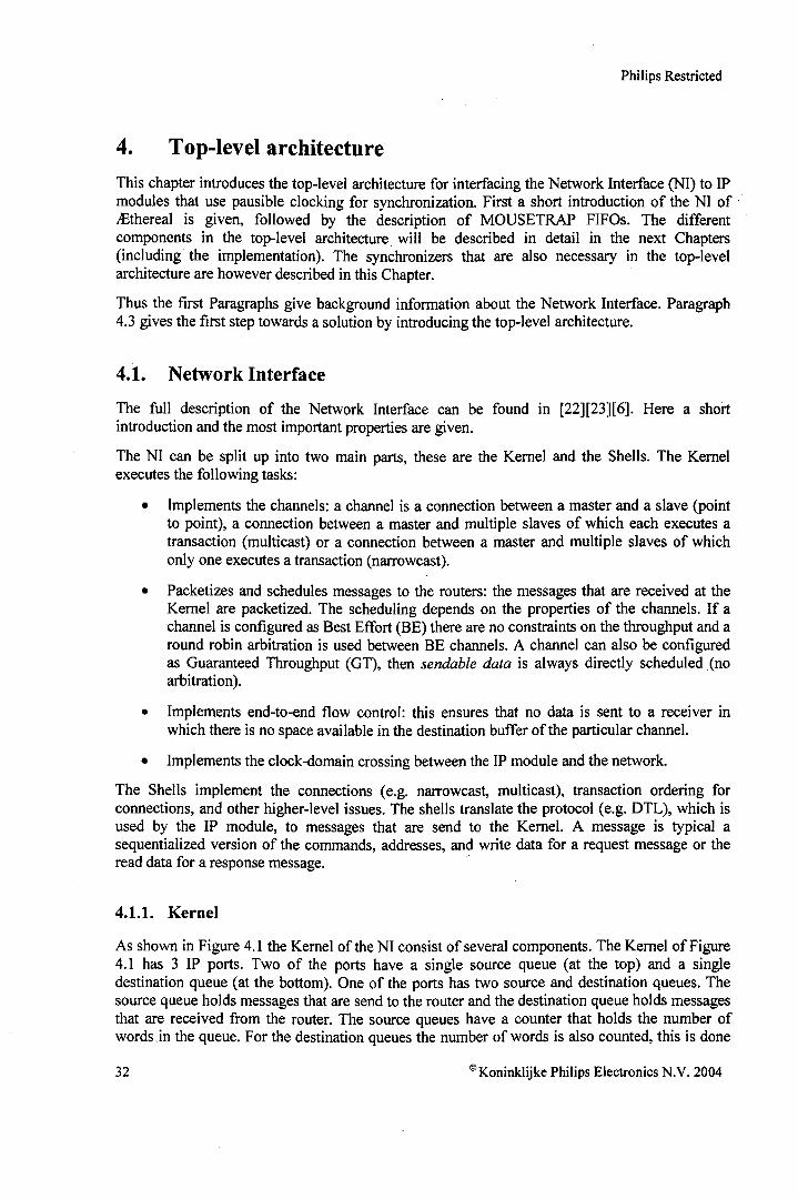
4.1. Network Interface
The full description of the Network Interface can be found in [22][23][6]. Here a shortintroduction and the most important properties are given.
The NI can be split up into two main parts, these are the Kernel and the Shells. The Kernelexecutes the following tasks:
• Implements the channels: a channel is a connection between a master and a slave (pointto point), a connection between a master and multiple slaves of which each executes atransaction (multicast) or a connection between a master and multiple slaves of whichonly one executes a transaction (narrowcast).
• Packetizes and schedules messages to the routers: the messages that are received at theKernel are packetized. The scheduling depends on the properties of the channels. If achannel is configured as Best Effort (BE) there are no constraints on the throughput and around robin arbitration is used between BE channels. A channel can also be configuredas Guaranteed Throughput (GT), then sendable data is always directly scheduled (noarbitration).
• Implements end-to-end flow control: this ensures that no data is sent to a receiver inwhich there is no space available in the destination buffer ofthe particular channel.
• Implements the clock-domain crossing between the IP module and the network.
The Shells implement the connections (e.g. narrowcast, multicast), transaction ordering forconnections, and other higher-level issues. The shells translate the protocol (e.g. DTL), which isused by the IP module, to messages that are send to the Kernel. A message is typical asequentialized version of the commands, addresses, and write data for a request message or theread data for a response message. '
4.1.1. Kernel
As shown in Figure 4.1 the Kernel of the NI consist of several components. The Kernel ofFigure4.1 has 3 IP ports. Two of the ports have a single source queue (at the top) and a singledestination queue (at the bottom). One of the ports has two source and destination queues. Thesource queue holds messages that are send to the router and the destination queue holds messagesthat are received from the router. The source queues have a counter that holds the number ofwords.in the queue. For the destination queues the number of words is also counted, this is done
in the Local Credit. The end-to-end flow control is implemented with credits. The Remote Spacecontains the number of empty data words of the remote destination queue for every connection(all connections are stored in a Connection Table). When data is send to the destination queue theRemote Space is decreased. When the data is consumed by the IP module of the destination theLocal Credit in the NI of the destination is increased. This Local Credit is send to the producer ofthe data and the value of the Local Credit that is received is added to the Remote Space of theproducer.
The term sendable data is already used in the previous Paragraph, the term is defined as theminimum between the data items. in the source queue and the value in the Remote Space. TheRequest Generator issues a signal specifying that the queue can be scheduled if the queuecontains sendable data. The scheduling is further handled by the GT Scheduler and the BEScheduler, dependent of the configuration of the specific channel.
One of the mechanisms that is used to optimise the NoC utilization is the usage of a thresholdmechanism to use longer packets. These thresholds are stored in the Limit Table. A threshold canbe overridden by the IP module with a so-called Flush signal. This is important, because it canhappen that the threshold is not reached while there is no new data send by the IP module andthere is data waiting to be send to the router. Then the data can remain in the queue indefinitely,because the IP module is waiting for an acknowledge from the destination.
4.1.2. Queues
The PIPOs in the Kernel are used as source and destination queues for the messages to and fromthe IP module. When the IP module has a clock domain that is not related to the clock domain ofthe Network Interface (or network) there is a clock domain crossing in the liccompanying queue.In this Paragraph the architecture of the source queue with its counter is described. The approachfor the destination queues is similar.
The source queue with its counter for counting the number of valid words in the FIFO is shownin Figure 4.2. For the source queues the write clock (wr_elk) is connected to the IP clock (IP_elk)and the read clock (rd_clk) is connected to the network clock (elk). The count register holds thenumber of valid data words in the FIFO and is used by the Request Generator in the Kernel. Therd_valid of the FIFO indicates if it is possible to read from the FIFO. Now this signal is notnecessary anymore, because the counter holds the information of the filling of the FIFO.
Figure 4.2: the source queue (rdt_niJifo) with counter (rdt_ni_cnt)
The value in the counter is incremented with one if the wr_valid and the wr_accept signals areboth true. And the value is decremented with the value of the send_words signal (from theRequest Generator) when the Flit Controller in the Kernel requests data from the selectedchannel (cnU'eadyulse and selected_channel are both true).
4.2. MOUSETRAP FIFOs
MOUSETRAP is an abbreviation for Minimal-Overhead Ultrahigh-SpEed Transition-signallingAsynchronous Pipeline and is introduced by [27]. This naming already gives a good idea whatkind of FIFO the MOUSETRAP is: a ripple-through FIFO. It uses an asynchronous controlscheme with transition signalling and therefore it can be implemented into a small silicon areaand gives a good performance for speed and power consumption. A "special" MOUSETRAPFIFO, which has two synchronous interfaces instead of asynchronous interfaces is used for thequeues in the Kernel [33]. The plain MOUSETRAP FIFO is described in this Paragraph and theone with the synchronous interfaces is described in Paragraph 4.2.1.
A MOUSETRAP FIFO is build up with a number of cells. Each cell has a control and a memorypart (see Figure 4.3) and the number of cells in serial gives the memory depth of the FIFO.
empty
Wdata Rdata
Figure 4.3: a single MOUSETRAP cell consisting ofa control and a memory part
The control part of a cell is build up with a single bit latch and an Exclusive-NOR gate. Thememory part is a number of latches storing the data, of course the width ofthe data is equal to thenumber of latches in the memory part of the cell. To illustrate the behaviour of a singleMOUSETRAP cell its STO is given in Figure 4.4. When the Wreq signal makes a transition andthe cell is empty (signal empty is true) then the write request action will be acknowledged with atransition of Wack. Now a data word has been written to the cell and a read request will be passedto the next MOUSETRAP cell with a transition of the Rreq signal. The empty signal will be falseuntil the read request is acknowledged with a transition of the Rack signal. The transition of theRack signal means that the next MOUSETRAP cell has stored the data and the sending cell is"made" empty by this acknowledgement. This is the first sequence in the STO (started from theinitial net marking). The second sequence behaves exactly the same, but now the transitions forthe request and acknowledge signals are inverted. The reason for this is that transition signallingis used in the MOUSETRAP cell.
Wack+empty+
t.Bal;& +t empty+ ~
empty- t.><~q- Wa~-
Figure 4.4: STG for a single MOUSETRAP cell
4.2.1. MOUSETRAP FIFO in a synchronous environment
To make use of the MOUSETRAP FIFO in a fully synchronous environment the input and theoutput stage of the asynchronous FIFO are adapted to the synchronous environment. Figure 4.5shows the connections between a MOUSETRAP FIFO and the adapters to interface a write clockand a read clock. In [33] two different implementations are presented for the adaptors.
Wdala Rdata
Figure 4.5: using adaptorsfor using a MOUSETRAP FIFO in a synchronous environment
Data is written to the FIFO when both signals wr_accept and wr_valid are true and there is arising clock edge on wrJlk. Data is read from the FIFO when both signals rd_accept andrd_valid are true. Figure 4.6 shows the timing arcs of the FIFO when it is implemented with theseadaptors. The arcs from the write clock (wr_elk) to the rd_data and rd_valid signals at the readside are only active if the FIFO is empty. The arc from the read clock (rd_clk) to the wr_acceptsignal is only active if the FIFO is full. This makes the FIFO without further hardware notsuitable to be used in designs where the read clock and the write clock are independent of eachother. If the FIFO is empty the rd data and the rd valid signals have to be synchronized to theclock of the receiver, because these signals are asynchronous to the this clock signal. If the FIFOis full the wr_accept signal has to be synchronized to the clock of the sender, because this signalis asynchronous to this clock signal.
With addition of synchronizers for the signals that cross the two independent clock domains aClock Domain Crossing (CDC) FIFO can be made. This kind of FIFO can be used safely in theKernel when the IP module has a clock domain that is independent from the clock domain of thenetwork.
A top-level architecture is chosen such that it is possible to synchronize an IP module with apausible clock domain to the Network Interface, which is clocked by the network clock. Thus theclock domain of the IP module and the clock domain of the network are assumed to becompletely independent of each other. Therefore different (independent) clock frequencies can beused between the two clock domains. The top-level architecture that is chosen is shown in Figure4.7. In the top-level architecture the complete IP module consist ofthe following blocks:
• Pausible clock generator.
• The original IP module.
• Translation Shells from the Network Interface (e.g. for DTL).
• One or more output controllers.
• One or more input controllers.
The clock generated with the pausible clock generator is distributed to the original IP module andthe Translation Shells. So the Translation Shells become part of the IP module. Every portbetween the Shells and the Kernel get an output controller and an input controller. The outputcontroller is interfaced to the source queue and the input controller is interfaced to the destination
queue of the Kernel. The source and destination queues are implemented with asynchronousFIFOs that use transition signalling. The MOUSETRAP FIFOs can be used here Gust everyasynchronous FIFO that uses transition signalling would do). For the source as well as for thedestination queue there is a push channel. For the source queue the output controller is theinitiator and therefore the request signal (Req) goes from the output controller to the FIFO. Forthe destination queue the FIFO is the initiator and therefore the request signal (Req) goes fromthe FIFO to the input controller.
ROUTER
FLUSH signals
Push ChannelSynchronizer
NetworkClock
Read sideSynchronizer
Write sideSynchronizer
<: ~.===========~>< >Clock domain IP module Asynchronous Clock domain Network
(pausible clock)
Figure 4. 7: top-level architecture for interfacing pausible clocked IP modules to the NI
Synchronizers are necessary for the interfacing of the asynchronous FIFO to the Kernel of the NI.Possible solutions for these synchronizers are introduced in [13]. Furthermore there issynchronization necessary for the counters that hold the number of valid data words in thequeues. (The counter for the destination queue is implemented in the Credit Controller.) The acksignals from the FIFOs at the IP side can be used to update the counters in the Kernel. Whensynchronizing these signals there is a certain latency introduced on these signals and it is possiblethat the number of valid words in the queue is higher than the value in the counter. When thishappens the threshold calculations in the Kernel will not be correct. However this is no problemfor the functioning of the Kernel, because the counter will eventually be updated and a newthreshold calculation is done. Thus the delay introduced by the counter comes back in thethreshold calculations and therefore also in the scheduling of packets in the Kernel. Next to thesynchronization of the signals for counting data words there is a Flush signal per source anddestination queue. All Flush signals have to be synchronized at the Kernel as well. More detailsabout these synchronizers are given in the next Paragraph.
Eventually with the current top-level architecture synchronizers are necessary at the Kernel of theNetwork Interface, three different kind of synchronizers are identified (as mentioned in theprevious Paragraph):
• Synchronizers for the asynchronous FIFOs.
• Synchronizers for the signals that can change the value of the counters, which count thenumber ofvalid words in the queues.
• Synchronizers for the Flush signals.
The use of synchronizers constraints the maximum clock frequency of the IP module. Themaximum frequency of the IP module must be lower than the frequency of the network clock. Ifthis is not the case data events from the IP module can not be sampled by the synchronizers in theKernel.
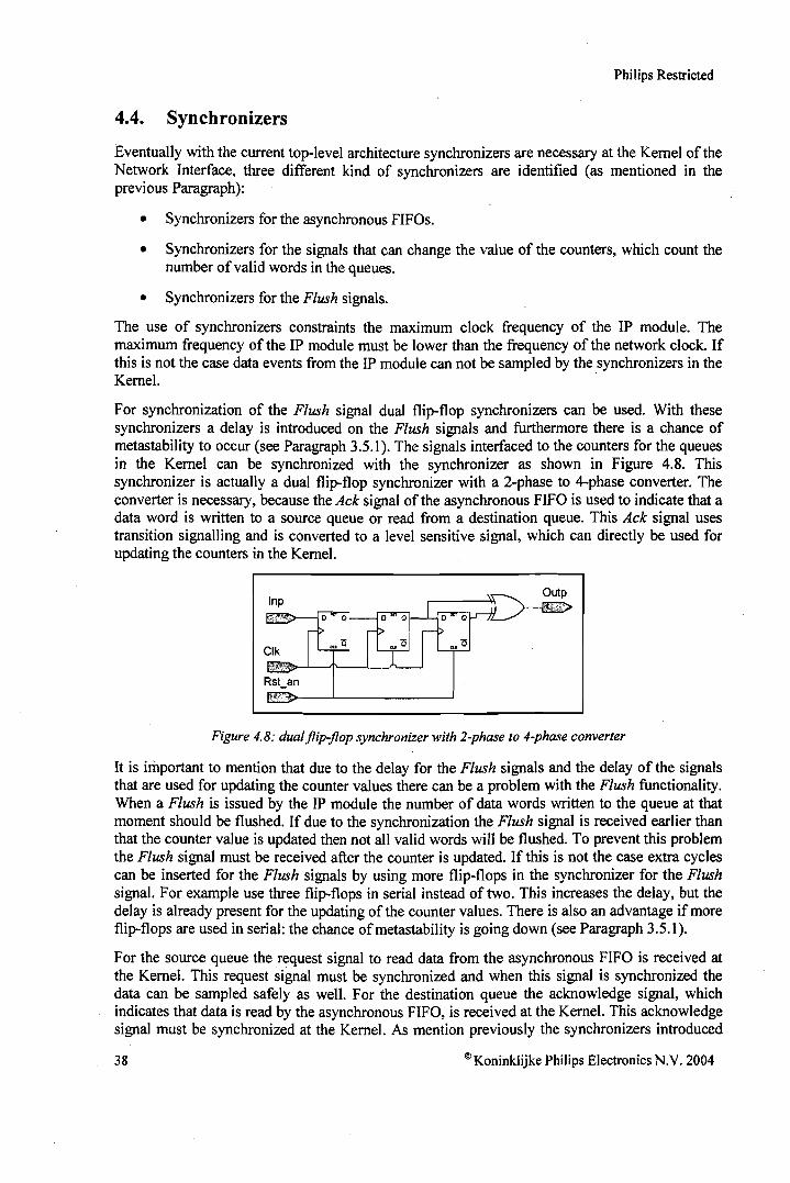
For synchronization of the Flush signal dual flip-flop synchronizers can be used. With thesesynchronizers a delay is introduced on the Flush signals and furthermore there is a chance ofmetastability to occur (see Paragraph 3.5.1). The signals interfaced to the counters for the queuesin the Kernel can be synchronized with the synchronizer as shown in Figure 4.8. Thissynchronizer is actually a dual flip-flop synchronizer with a 2-phase to 4-phase converter. Theconverter is necessary, because the Ack signal of the asynchronous FIFO is used to indicate that adata word is written to a source queue or read from a destination queue. This Ack signal usestransition signalling and is converted to a level sensitive signal, which can directly be used forupdating the counters in the Kernel.
Inp
elk
Outp
Figure 4.8: dualflip-flop synchronizer with 2-phase to 4-phase converter
It is important to mention that due to the delay for the Flush signals and the delay of the signalsthat are used for updating the counter values there can be a problem with the Flush functionality.When a Flush is issued by the IP module the number of data words written to the queue at thatmoment should be flushed. If due to the synchronization the Flush signal is received earlier thanthat the counter value is updated then not all valid words will be flushed. To prevent this problemthe Flush signal must be received after the counter is updated. If this is not the case extra cyclescan be inserted for the Flush signals by using more flip-flops in the synchronizer for the Flushsignal. For example use three flip-flops in serial instead of two. This increases the delay, but thedelay is already present for the updating of the counter values. There is also an advantage if moreflip-flops are used in serial: the chance ofmetastability is going down (see Paragraph 3.5.1).
For the source queue the request signal to read data from the asynchronous FIFO is received atthe Kernel. This request signal must be synchronized and when this signal is synchronized thedata can be sampled safely as well. For the destination queue the acknowledge signal, whichindicates that data is read by the asynchronous FIFO, is received at the Kernel. This acknowledgesignal must be synchronized at the Kernel. As mention previously the synchronizers introduced
in [13] can be used for the asynchronous signals of the FIFOs. These synchronizers use so-calledWAIT components. For completeness these WAIT components are described with STGs in thenext Paragraph.
4.4.1. WAIT components
WAIT components can be used to synchronize handshake signals [13]. The basic WAITcomponent is the WAIT4. This component is a Mutual Exclusion element with only one output.The inverted clock is connected to the first input of the Mutual Exclusion element and the signalsynchronized to the phase of the clock signal is connected to the second input. Only the secondoutput (corresponding to the signal that must be synchronized) is available. Figure 4.9 shows theWAIT4 component with the corresponding STG. The internal signal dummy is used in the STG toseparate the c/k- and the clk+ transitions. A request (low-to-high transition of Req) will onlypropagate through the WAIT4 component when the clock signal has a high phase. When the clocksignal has a low phase and a request arrives, then this request is blocked until the clock signalrises.
elk
Req Ack
Figure 4.9: WAIT4 component with STG
The WAIT4 component is suitable to synchronize handshake signals that use 4-phasehandshaking, but when 2-phase handshaking is used (e.g. MOUSETRAP) a 2-phase WAITcomponent must be used. Figure 4.10 shows a 2-phase WAIT component, also called WAIT2. Itis build up with a WAIT4 component, a latch and an Exclusive OR-gate. The behaviour of theWAIT2 component is described with a STG (see Figure 4.11).
Ack
Figure 4.10: WAIT2 component
In the right part of the STG the behaviour of the WAIT4 component is found again. Instead of theReq and Ack signals it now has the signals d and e. The signal that is synchronized is named Req
again, the synchronized result is the signal Ack. Now a rising as well as a falling transition of theReq signal will be blocked if the clock signal has a low phase. A transition is blocked until theclock has a high phase again.
The WAIT4 and the WAIT2 component both use synchronization by the phase of the clock signal,but it is also possible to synchronize by the edge of the clock signal with WAIT components.With edge synchronization a better performance can be achieved. A chance of metastability.exists when WAIT components are used for synchronization, because metastability occurs in theMutual Exclusion element when both inputs arrive at the same moment in time.
The pausible clock generator is an essential component when clock pausing is used forsynchronization purposes. The circuit that is used in the top-level architecture to generate a .pausible clock signal for the IP module is described in this Chapter. First the basic circuit of thispausible clock generator is described. Then extensions to this circuit are discussed. Theseextensions are necessary for multiple request signals from I/O controllers that request to pausethe cl.ock signal. Two approaches to accommodate multiple request signals are discussed. Onlyone of the two is working correctly under all conditions of the input signals and is therefore thepreferred circuit. Furthermore the timing of the pausible dock generator is described. This timingbehaviour is important for the interfacing of the VO controllers to the IP module and the pausibleclock generator.
5.1. Basic circuit
The basic circuit of the pausible clock generator that is used for the pausible clocked IP module isshown in Figure 5.1. The basic circuit is actually a ring oscillator with an arbiter in the loop. Thering oscillator is build up with a delay line and an inverter. The delay line can be programmable,such that different frequencies can be generated. This is a necessity if dynamic frequency scalingis used [14][25][26]. A Mutual Exclusion element is used for the arbitration. The circuit also hasan asynchronous reset, which is controlled by the rst_an signal. When extensions of the basiccircuit are discussed later on in this Chapter this reset is not shown for keeping things a bitsimpler. Every pausible clock generator should have a reset to start the clock generation properly.Three intermediate signals are also named in the basic circuit ofFigure 5.1., these are:
• clk_n: the output signal ofthe ring oscillator. This signal is inverted to produce the actualclock signal (elk), thus clk_n is the inverted clock signal.
• clk_d: this is the delayed clk_n signal.
• clk_m: the signal clk_d after the propagation through the Mutual Exclusion element.
Req Gnt
elk
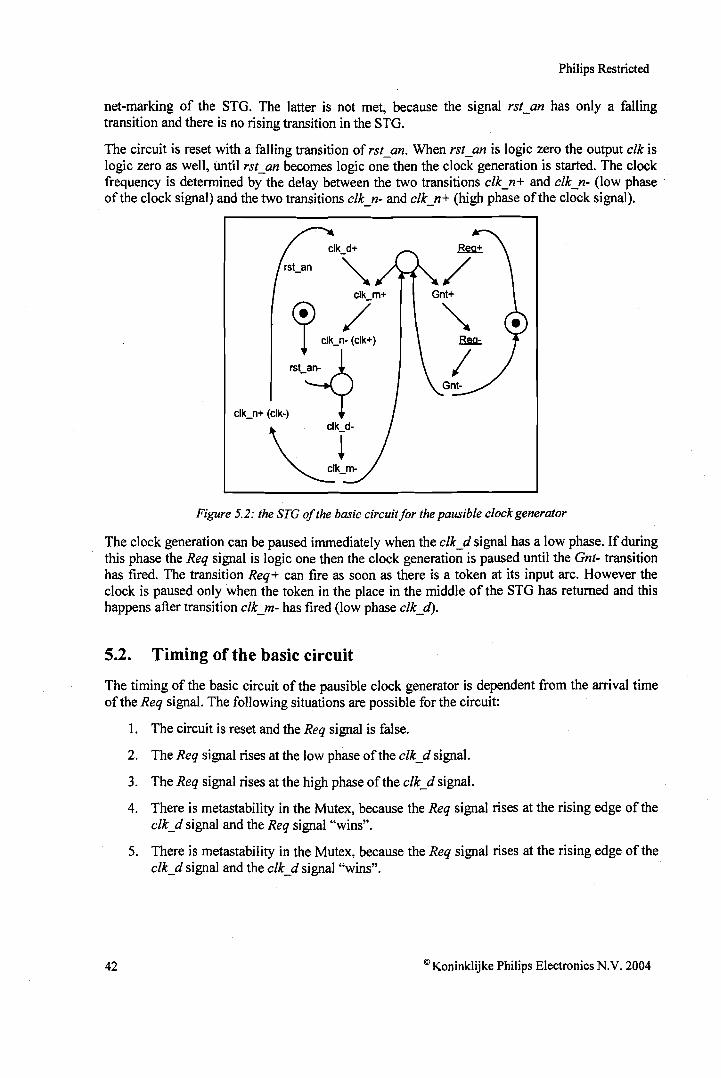
Figure 5.1: the basic circuit for the pausible clock generator
With the inputs, outputs and intermediate signals of the basic circuit for thepausible clockgenerator a STG can be made that describes the behaviour of the circuit. This STG is shown inFigure 5.2. The reset behaviour of the basic circuit is also modelled in the STG. The result of thisis that the STG does not comply to the liveness property and the single-cycle-transitions propertyof STGs. The former is not met, because transition rst_an- can not be fired from every reachable
net-marking of the STG. The latter is not met, because the signal rst_an has only a fallingtransition and there is no rising transition in the STG.
The circuit is reset with a falling transition of rst_an. When rst_an is logic zero the output elk islogic zero as well, until rst_an becomes logic one then the clock generation is started. The clockfrequency is detennined by the delay between the two transitions elk_n+ and elk_n- (low phase 'of the clock signal) and the two transitions elk_n- and elk_n+ (high phase ofthe clock signal).
Figure 5.2: the srG ofthe basic circuit for the pausible clock generator
The clock generation can be paused immediately when the elk_d signal has a low phase. If duringthis phase the Req signal is logic one then the clock generation is paused until the Gnt- transitionhas fired. The transition Req+ can fire as soon as there is a token at its input arc. However theclock is paused only when the token in the place in the middle of the STG has returned and thishappens after transition elk_m- has fired (low phase elk_d).
5.2. Timing of the basic circuit
The timing of the basic circuit of the pausible clock generator is dependent from the arrival timeof the Req signal. The following situations are possible for the circuit:
1. The circuit is reset and the Req signal is false.
2. The Req signal rises at the low phase of the elk_d signal.
3. The Req signal rises at the high phase of the elk_d signal.
4. There is metastability in the Mutex, because the Req signal rises at the rising edge of theelk_d signal and the Req signal "wins".
5. There is metastability in the Mutex, because the Req signal rises at the rising edge of theelk_d signal and the elk_d signal "wins".
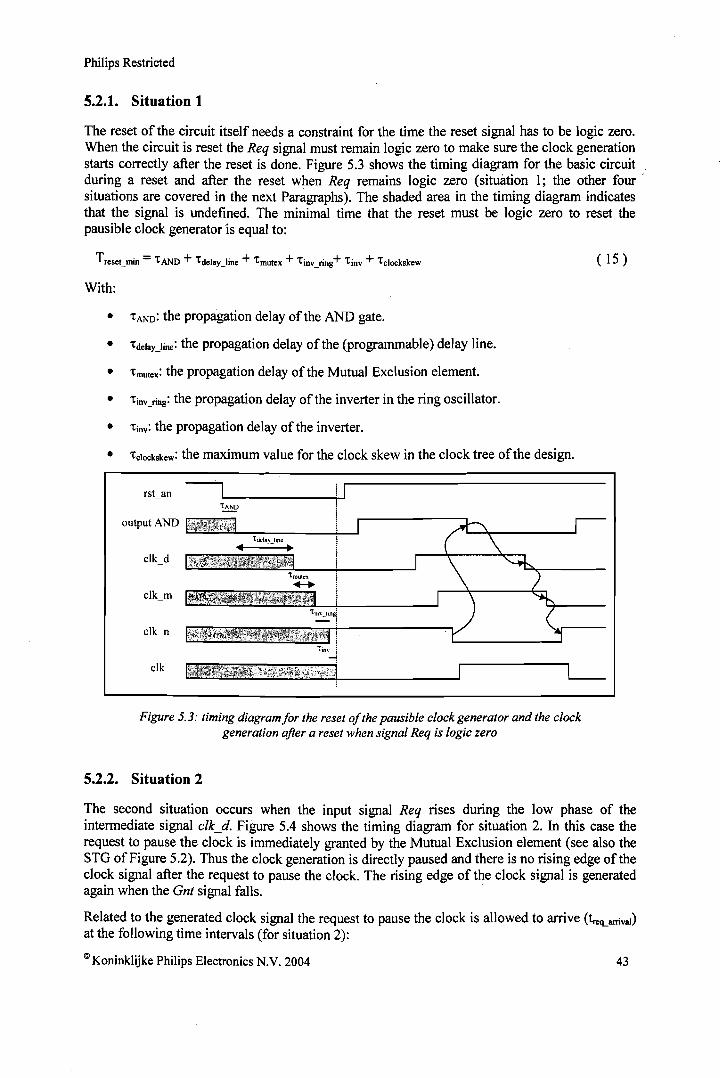
The reset of the circuit itself needs a constraint for the time the reset signal has to be logic zero.When the circuit is reset the Req signal must remain logic zero to make sure the clock generationstarts correctly after the reset is done. Figure 5.3 shows the timing diagram for the basic circuitduring a reset and after the reset when Req remains logic zero (situation 1; the other four .situations are covered in the next Paragraphs). The shaded area in the timing diagram indicatesthat the signal is undefined. The minimal time that the reset must be logic zero to reset thepausible clock generator is equal to:
( IS)
With:
• 'tAND: the propagation delay ofthe AND gate.
• 'tdelay_line: the propagation delay of the (programmable) delay line.
• 'tmutex: the propagation delay of the Mutual Exclusion element.
• 'tiny_ring: the propagation delay of the inverter in the ring oscillator.
• 'tiny: the propagation delay of the inverter.
• 'tclockskew: the maximum value for the clock skew in the clock tree ofthe design.
tinY rine:!...:...~
output AND
elk d
elk m
elk n
elk
Figure 5.3: timing diagram for the reset ofthe pausible clock generator and the clockgeneration after a reset when signal Req is logic zero
5.2.2. Situation 2
The second situation occurs when the input signal Req rises during the low phase of theintermediate signal elk_d. Figure SA shows the timing diagram for situation 2. In this case therequest to pause the clock is immediately granted by the Mutual Exclusion element (see also theSTG ofFigure 5.2). Thus the clock generation is directly paused and there is no rising edge oftheclock signal after the request to pause the clock. The rising edge of the clock signal is generatedagain when the Gnt signal falls.
Related to the generated clock signal the request to pause the clock is allowed to arrive (~arrival)
at the following time intervals (for situation 2):
With the assumptions that at moment zero the clock signal rises, the period of the clock signal isT and that the duty cycle ofthe clock signal is 50%.
elk I'till"
'tmUh,'" 'tdclav line + 'rAND
III ~
Req
Gnt
Figure 5.4: pausing the clock generation when signal Req arrives in the low phase ofintermediate signal clk_d
5.2.3. Situation 3
Figure 5.5 shows the timing diagram for situation 3. The request to pause the clock generationarrives during the high phase of elk_d. Now the request to pause the clock is not grantedimmediately as is the case for situation 2, because the Mutual Exclusion element is blocking theReq signal until the elk_d signal becomes false again. It is important to note that for situation 3there is the possibility that there is a rising edge of the clock signal within the request/grantsequence. This happens when the Req signal arrives in the shaded area ofthe high phase of signalelk_d (see Figure 5.5). This shaded area starts at the rising edge of elk_d and has the followingwidth:
elk I'tin"
elk_d
elk m
elk n
Req
Gnt
( 17)
L
44
Figure 5.5: pausing the clock generation when signal Req arriving in the high phase ofintermediate signal clk_d
With the assumptions that at moment zero the clock signal rises, the period of the clock signal is ..T and that the duty cycle of the clock signal is 50%. Furthermore here is assumed that there is norising clock edge allowed during the request/grant sequence to pause the clock signal. Togetherwith the allowed arrival time intervals for the request in situation 2 this gives the completeinterval in which a request is allowed to arrive (with the same aforementioned assumptions):
o< 4elLarriyai < T - 'tmutex - 'tinYJing - 'tiny
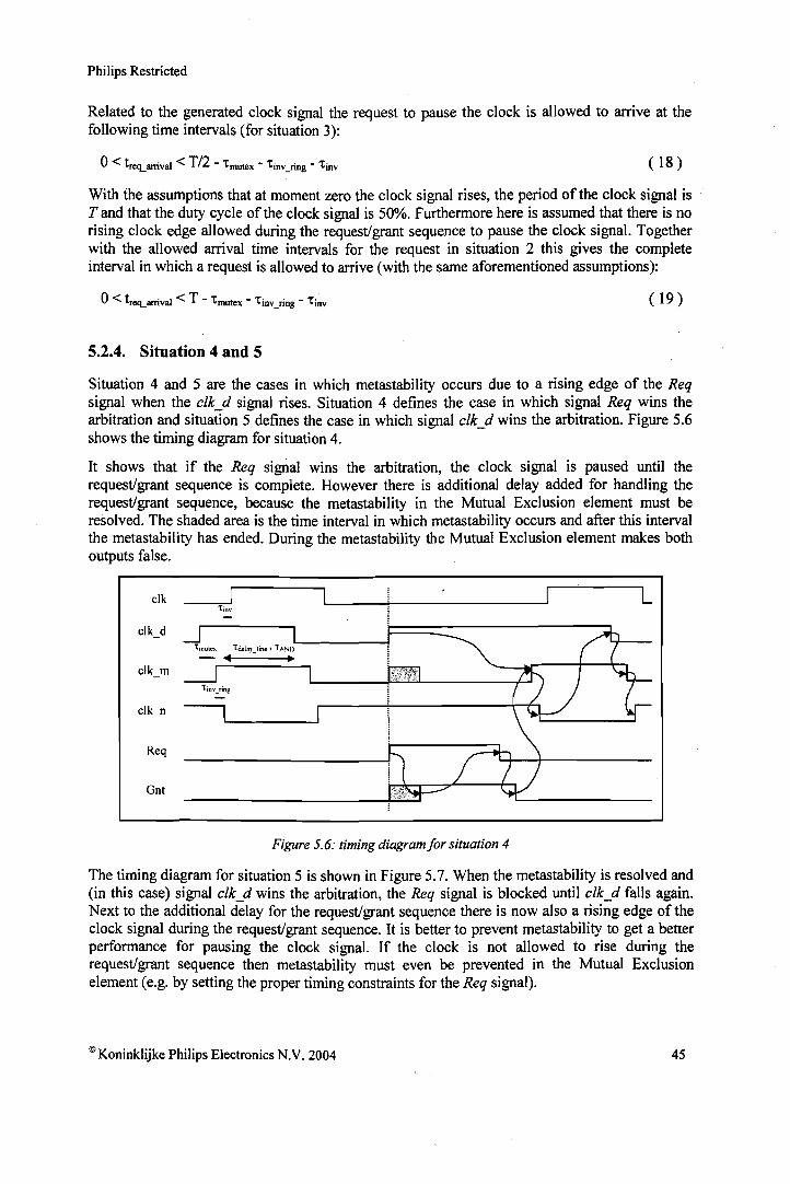
5.2.4. Situation 4 and 5
(19)
Situation 4 and 5 are the cases in which metastability occurs due to a rising edge of the Reqsignal when the elk_d signal rises. Situation 4 defines the case in which signal Req wins thearbitration and situation 5 defines the case in which signal elk_d wins the arbitration. Figure 5.6shows the timing diagram for situation 4.
It shows that if the Req signal wins the arbitration, the clock signal is paused until therequest/grant sequence is complete. However there is additional delay added for handling therequest/grant sequence, because the metastability in the Mutual Exclusion element must beresolved. The shaded area is the time interval in which metastability occurs and after this intervalthe metastability has ended. During the metastability the Mutual Exclusion element makes bothoutputs false.
elk
elk n
Req
Gnt
r-----:t"....inv
tmutex tdela" line + tAN/)..- .L
Figure 5.6: timing diagramfor situation 4
The timing diagram for situation 5 is shown in Figure 5.7. When the metastability is resolved and(in this case) signal elk_d wins the arbitration, the Req signal is blocked until elk_d falls again.Next to the additional delay for the request/grant sequence there is now also a rising edge of theclock signal during the request/grant sequence. It is better to prevent metastability to get a betterperformance for pausing the clock signal. If the clock is not allowed to rise during therequest/grant sequence then metastability must even be prevented in the Mutual Exclusionelement (e.g. by setting the proper timing constraints for the Req signal).
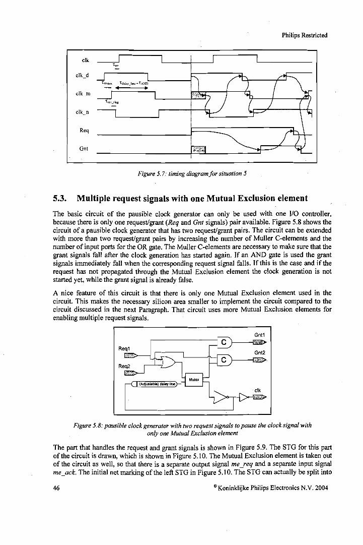
5.3. Multiple request signals with one Mutual Exclusion element
The basic circuit of the pausible clock generator can only be used with one I/O controller,because there is only one request/grant (Req and Gnt signals) pair available. Figure 5.8 shows thecircuit of a pausible clock generator that has two request/grant pairs. The circuit can be extendedwith more than two request/grant pairs by increasing the number of Muller C-elements and thenumber of input ports for the OR gate. The Muller C-elements are necessary to make sure that thegrant signals fall after the clock generation has started again. If an AND gate is used the grantsignals immediately fall when the corresponding request signal falls. If this is the case and if therequest has not propagated through the Mutual Exclusion element the clock generation is notstarted yet, while the grant signal is already false.
A nice feature of this circuit is that there is only one Mutual Exclusion element used in thecircuit. This makes the necessary silicon area smaller to implement the circuit compared to thecircuit discussed in the next Paragraph. That circuit uses more Mutual Exclusion elements forenabling multiple request signals.
Gnt1
cGnt2
elk
Figure 5.8: pausible clock generator with two request signals to pause the clock signal withonly one Mutual Exclusion element
The part that handles the request and grant signals is shown in Figure 5.9. The STG for this partof the circuit is drawn, which is shown in Figure 5.10. The Mutual Exclusion element is taken outof the circuit as well, so that there is a separate output signal meJeq and a separate input signalme_ack. The initial net marking of the left STG in Figure 5.10. The STG can actually be split into
two separate STOs working in parallel, one for the Reql/Gntl pair and one for the Req2/Gnt2pair. Thus if these two are combined in a single STG to describe the behaviour of the circuit ofFigure 5.9 there are two initial tokens in the STG. These two tokens can then fire transitionsindependent of each other. A problem with the circuit can occurs when the net marking of theright STG in Figure 5.10 is considered. The net marking can cause a glitch on the meJeq or .me_ack signal. For example if the transition meJeq+ fires the transition meJeq- can fireimmediately after this because of the second token in the STG. The possibility of these glitches tooccur in the circuit makes the circuit not suitable to be used as a pausible clock generator,because it will make the clock pausing not robust.
Gnt1
Gnt2
Figure 5.9: the request/grant part ofthe pausible clock generator with two request/grantpairs and only one Mutual Exclusion element
Gn12+
•&lI2:,
Gnl1+ Gn12+
• •~ &lI2:,
~
Gnl1+
•~~
Figure 5.10: the STG ofthe request/grant part ofthe pausible clock generator; left sro:initial net marking; right sro: net marking, which can cause glitches
5.4. Multiple request signals with multiple Mutual Exclusion elements
An alternative for accommodating more than one request/grant pair for pausing the clock signalis shown in Figure 5.11. The circuit uses a Mutual Exclusion element for every request/grant pair.In the circuit there are two request/grant pairs, thus there are two Mutual Exclusion elements .used. The grant signals, me--Pltl and me--Plt2, are used for the clock generation and arecombined with the AND gate. If one of the two is not granted,· because a request to pause theclock generation is received, then the output of the AND gate becomes false and the clockgeneration is paused. This pausible clock generator can always be extended with morerequest/grant pairs. This is achieved by adding a Mutual Exclusion element for everyrequest/grant pair and adding an input port for the AND gate. The Mutual Exclusion elements areconnected in parallel and therefore there is no additional delay when there are more MutualExclusion elements inserted. However the chance that the clock generation will be paused islarger with more request/grant pairs (this is a system level issue). The behaviour of this pausibleclock generator is specified completely with a STG, which is shown in Figure 5.12. In contrary tothe circuit introduced in Paragraph 5.3, no glitches can occur in this circuit.
Gn12 ~iJ£.iJ--__-------,
Req2~t>------,
Gnt1 ~r:wi'1c'l!1-------,
Figure 5.11: the pausible clock generator with two request/grant pairs and two MutualExclusion elements
One output controller is developed. This chapter describes the interfacing, the behaviour and thetiming specification of this output controller. The output controller is specified with a Signal .Transition Graph (STG). The tool Petrify is used to synthesize the STG in equations forgeneralized C-elements. The implementation of this output controller in standard cell design isdescribed in Chapter 8.
6.1. Interface
The interfacing of the output controller to the IP module, the pausible clock generator and theasynchronous FIFO is shown in Figure 6.1. The complete interface of the output controllerconsists ofthe following inputs and outputs:
• Inputs: elk, wr_valid, Gntl, ack.
• Outputs: Reql, req.
The elk signal is also interfaced to the output controller, but the clock signal is only used toresample the wr_valid signal as is explained in the timing specification of the output controller(see Paragraph 6.3). The wr_valid signal indicates when data is send to the asynchronous FIFO.The output controller controls the handshaking with the asynchronous FIFO and can request topause the generation of the clock signal with the Reql signal. The request to pause the clock isacknowledged with the Gntl signal. The handshaking with the pausible clock generator is levelsensitive (also called 4-phase handshaking) and for the communication with the asynchronousFIFO transition signalling (also called 2-phase handshaking) is used. The data signals from the IPmodule are directly connected to the asynchronous FIFO.
Pausible clock generator IIelk..
V Req1 Gnt1
IPmodule L......+
Outputreq
wr_valid AsynchronousController ack
FIFOwr_data
Figure 6.1: interfacing ofthe output controller to the IP module, the pausible clockgenerator and the asynchronous FIFO
The output controller is an Asynchronous Finite State Machine (AFSM) with some additionallogic. The STG for the AFSM is shown in Figure 6.2 and describes the behaviour of the outputcontroller. There is a small difference with the interface and the STG for the AFSM: the wr_validsignal at the interface is not used in the STG, instead the signal valid is used. There is only adifference in timing, which becomes clear in Paragraph 6.3 where the timing specification of theoutput controller is defined. The valid signal has the same meaning as the wr_valid signal, whichis the indication that new data must be send to the asynchronous FIFO. The STG also contains aninternal signal called dummy. This signal is inserted to prevent that the transition valid- isfollowed by the transition valid+. Furthermore the STG has two almost identical parts which areconnected via the valid+ transition. The only difference between the two parts is the risingtransitions for the signals req and ack in one part and the falling transition for these signals in theother part. The reason for this is that these signals use transition signalling with the asynchronousFIFO.
The behaviour of the output controller is then as follows (see also the timing diagram in Figure6.3):
• After the firing of transition valid+ the Req1 signal will rise (transition Req1 +) to requestto pause the elk signal.
• When this is granted with the Gnt1 signal from the pausible clock generator, thetransition req+ fires to request writing to the asynchronous FIFO. The transition ack+will fire when the FIFO consumed the data.
• The elk signal can now be activated again by making the Req1 signal false (transitionReq1-) and when the Gntl- transition fires the output controller waits for a new risingedge of the valid signal. Before the valid+ transition can fire again the valid- transitionmust fire first (including the transitions for the dummy signal), as is shown in the parallelbranch in Figure 6.2.
• The sequence of transitions is repeated, but now with a high-to-Iow transition for the reqand ack signals, because the asynchronous FIFO uses transition signalling. When thissequence is complete the STG begins at the starting point again.
elk
valid------'
Req1___....J
Gnt1 ----J
req ----J
ack
Figure 6.3: timing diagram for the output controller
The complete sequence of writing a data word to the asynchronous FIFO should be done within asingle clock cycle. Then the clock signal is never paused when there is space in the FIFO. If theFIFO is full, the elk signal will be paused and the IP module must wait until there is spaceavailable in the FIFO. The first data word written in Figure 6.3 shows that writing a data word tothe asynchronous FIFO can be done within one clock cycle, because here the clock signal is notpaused. However the second word that is written pauses the clock signal, because the FIFO isfull. When the transition of the ack signal is received the data is consumed by the FIFO and theclock is started again.
The input file for Petrify and the resulting equations for the output controller can be found inAppendixB.
6.3. Timing specification
The wr_valid signal from the IP module is interfaced to the output controller and the wr_datasignals are interfaced to the asynchronous FIFO (see Figure 6.1 and Figure 6.4). Figure 6.4 showsthe output controller with the AFSM and the surrounded logic. The logic is necessary to translatethe wr_valid signal to the valid signal that is connected to the AFSM. It must be possible to write
a data word to the asynchronous FIFO every clockcycle, so that there is a high throughput for thedata. Therefore timing constraints for the interfacing ofthe output controller are necessary:
1. The valid signal must rise and fall in a single clock cycle (as the defined in the STG).
2. When the valid signal rises the wr_data must be stable.
3. When a request to pause the clock signal is send to the pausible clock generator, no risingedge of the clock signal is allowed until the request is withdrawn.
elk
Figure 6.4: the pathsfor the valid and the wr_data signalsfrom the IP module to the outputcontroller
The wr_valid signal does not have a rise and fall transition in a single clock cycle. To generatethis behaviour for the valid signal an extra flip-flop is used (FF2), which has an asynchronousreset port. This port is controlled by the normal reset signal (rst_an), but also with the ReqIsignal. The latter becomes true after the valid signal becomes true (see STG) and is received bythe AFSM. Now the valid signal will always fall after its rising transition and when the ReqIsignal is false again a new valid+ transition can be produced with FF2• This as a whole solvesconstraint 1.
FF2 samples the input at a different phase than the phase of the elk signal, which is used in the IPmodule. This phase difference is used to insert extra delay for the valid signal to make a risingtransition, because when the valid+ transition occurs the data that is send to the asynchronousFIFO must be stable. The minimal value for the delay 't1 can be calculated with (constraint 2):
(20 )
With:
• tp_lJ1: the propagation delay of FF}.
• tpJogicl: the propagation delay of logic}.
• tp_wirel: the propagationdelay ofthe wires between FF} and FF2•
• tp_wire2: the propagation delay of the wires between FF3 and the asynchronous FIFO.
• tpJogic2: the propagation delay of logic2.
For constraint 3 the used pausible clock generator must guarantee that there is no rising edge ofthe clock signal when a request to pause the clock generation is send. When the pausible clock .generator of Paragraph 5.4 is used, then putting the proper timing constraints on the Reql (andReq2) signals answers constraint 3.
The time at which the Reql signal rises after the last rising clock edge can be determined with:
(21 )
With:
• tp_wntroller: the propagation delay for the output controller to make a low-to-high transitionfor signal Req1.
• tp_ft2: the propagation delay ofFF2•
To apply these timing constraints in a design flow there is the problem that not all delays areknown during design time (e.g. the delay of wires). A solution for this is that a fixed value fordelay 't) is taken. A good choice is to take 't) equal to half the clock period. Then FF2 can simplybe a negative-edge-triggered flip-flop and this gives the timing constraint (with Tthe clock periodand assuming a duty cycle of 50%):
(22 )
This constraint is set during design time and can be checked after layout with static timinganalysis. The timing constraint for all request signals to pause the clock is then:
(23 )
With the following delays in the pausible clock generator (remember the timing of the pausibleclock generator):
• 'tmutex: the propagation delay ofthe Mutual Exclusion element.
• 'tinv_ring: the propagation delay of the inverter in the ring oscillator.
Two input controllers' are developed. This Chapter describes the interfacing, the behaviour andthe timing specification of these input controllers. The same procedure as for the output 'controller is followed. Thus both input controllers are defined with STGs and synthesized to.equations. The input controller that is described first uses an extra latch stage to keep the inputdata stable such that the data can be sampled by the IP module. The other input controller usesthe asynchronous FIFO to keep the data stable. Only the input controller, which does not use anauxiliary latch stage is implemented and this implementation is described in Chapter 8.
7.1. Input Controller with auxiliary latches
The input controller is first designed with the use of an extra latch stage that keeps the data stablewhen this data is sampled by the IP module. The input controller can then directly control theselatches. The advantage of using auxiliary latches is that the control of these latches is completelydecoupled from the 2-phase handshaking of the FIFO via the input controller. However the use ofauxiliary latches makes the AFSM in the input controller more complex and also the timing forthe interface is more complex.
The latches can be implemented with standard cell latches with a single enable signal (a reset isnot necessary). However if standard cells are used this will consume quite some silicon area. Itwould be better to design the latches together with the asynchronous FIFO, so that both aredesigned full custom.
7.1.1. Interface
The interfacing of the input controller to the IP module, the pausible clock generator, theauxiliary latch stage and the asynchronous FIFO is shown in Figure 7.1. The complete interface
. of the input controller consists ofthe following inputs and outputs:
• Inputs: elk, rd_accept, Gnt2, req.
• Outputs: Req2, ack, en.
For the rd_valid signal a similar approach is taken as for the wr_valid signal of the outputcontroller. The elk signal is used to resample the rd_valid signal as is explained further in thetiming specification of the input controller. The rd_valid signal indicates that the IP modulewants to read a data word from the FIFO. Furthermore the 4-phase handshaking with the pausibleclock generator is the same as for the output controller. The Req2 signal is used to send a requestto pause the clock and this is granted by the pausible clock generator with the Gnt2 signal. The 2phase handshaking with the asynchronous FIFO is different compared to the output controller.Now the req signal is send by the asynchronous FIFO, which is therefore the initiator and thesender of the data. The input controller will acknowledge to the asynchronous FIFO with the acksignal that the data has been consumed by the IP module. As mentioned before the latches areused to sample the data from the asynchronous FIFO (rd_data signals). This is done by settingthe latches transparent by making the enable signal (en) logical one. When the data is sampledthe latches are made opaque by making the enable signal (en) logical zero.
Figure 7.1: interfacing ofthe input controller with auxiliary latches to the 1P module, thepausible clockgenerator and the asynchronous FiFO
7.1.2. Behaviour
The STO of the input controller with auxiliary latches is shown in Figure 7.2. The following threestarting places arepresent in the STO:
• The place before transition req+.
• The place before transition Req2+.
• The place before transition accept+ .
This STO also has two parts which are the same accept for the transitions of the handshakesignals for the asynchronous FIFO (due to the 2-phase handshaking). The accept signal in theSTO has the same function as the rd_accept signal as described before. The behaviour of theinput controller with auxiliary latches is then as follows (see also the timing diagram of Figure7.3):
• After the firing of transition accept+ a request to the pausible clock generator is send topause the clock (transition Req2+).
• In the meantime a request from the asynchronous FIFO can be received (or is alreadyreceived earlier) and when the low-to-high transition ofthe Gnt2 signal is received by theinput controller the transition en+ fires to set the latches transparent.
• The enable signal is delayed (as explained in the timing specification in the nextParagraph) and after this delay (firing of transition en_d+) the pausing of the clock isstopped (firing of transitions Req2- and Gnt2-).
• When the latch enable signal (en) and the delayed version of this signal (en_d> are madefalse, then the acknowledge is send to the asynchronous FIFO with the ack signal. Thisacknowledge indicates that the data is consumed by the latches.
• Parallel to the sequence of steps above the accept signal must have a high-to-lowtransition. When the transition accept+ fires again the complete sequence is repeated, butnow with the inverted transitions of the request (req) and acknowledge (ack) signals ofthe asynchronous FIFO.
• After the second sequence the STG starts over again from the starting point(s).
dummy+
dumow-~ .
accept-
~
accept+
/
dummy-~ .
accept-
~
TGnt2+
Ireq-
'"en+
~en d+
1Req2-
~Gnt2-
Ien-
Ien d-r
Gnt2+
Ien+
~en d+
1Req2-
\ ~Gnt2- accept+
~ ~ ~en-
~en d-
tack+
\
ack-,req+
Figure 7.2: STGfor the input controller with auxiliary latches
Figure 7.3: timing diagram for the input controller with auxiliary latches
The complete sequence of reading a data word from the asynchronous FIFO should be donewithin a single clock cycle. The clock signal is never paused when there is valid data in the FIFO.However if the FIFO is empty then the elk signal is paused and the IP module must wait untilthere is valid data available in the FIFO. Figure 7.3 shows that the first data word that is readfrom the asynchronous FIFO can be read within a single clock cycle, so the clock signal is notpaused. When the second data word is read the clock signal is paused, because the transitionaccept+ fires when the FIFO is empty. There is data available when the req signal makes atransition again and then the read sequence is continued.
The input file for Petrify and the resulting equations for this input controller can be found inAppendix C.
7.1.3. Timing specification
Next the timing specification is given for the input controller with an auxiliary latch stage. Therd_accept signal is interfaced to the input controller and the rd_data signals are interfaced fromthe asynchronous FIFO to the extra latch stage (see Figure 7.4). The latch stage is controlled bythe input controller with the en signal and the data from the latch stage is interfaced to the IPmodule.
The en signal is delayed with 't3 when the en signal has a low-to-high transition. The herebygenerated signal is called en_d and is send back to the AFSM of the input controller. The en_dsignal is generated by using an AND gate with as input the en signal and the delayed en signal.The following timing constraints are necessary for this input controller:
1. The accept signal must rise and fall in a single clock cycle (as defined in the STG).
2. When a request is received from the asynchronous FIFO (transition of the req signal) thedata must be kept stable long enough to be sampled correctly by the receiving flip-flopsof the IP module (setup and hold constraints).
3. When a request to pause the clock signal is send to the pausible clock generator, no risingedge of the clock signal is allowed until the request is withdrawn.
Figure 7.4: the paths for the accept and the rd_data signals to andfrom the input controllerwhen auxiliary latches are used
Constraint I is similar to constraint I of the output controller and therefore an extra flip-flop(FF]) is used to generate the accept signal. This flip-flop can be reset with the normal reset signal(rst_an) and the Req2 signal from the AFSM. The latter makes sure that the falling transition ofthe accept signal automatically occurs after its rising transition is received by the AFSM. Theminimal value for the delay 't] can be calculated with:
(24 )
With:
• tp_ff1: the propagation delay ofFF,.
• tpJogicJ: the propagation delay of the logic,.
• tp_wirel: the propagation delay of the wires between FF, and FF].
• tsu_ft2: the setup time ofFF].
The signal en_d determines when the clock can be enabled again. The delay 't3 is then used tomake sure that the data from the FIFO can arrive at FFJ before the rising clock edge. The
.minimal value for delay 't3 can be calculated with (constraint 2):
(25 )
With:
tp_logic2: the propagation delay of logic].
tp_latch: the propagation delay ofthe latch.
tp_wire2: the propagation delay of the wires between FFJ and the asynchronous FIFO.
The hold constraint for the rd_data is automatically met if (constraint 2):
(26 )
With:
• th_tl3: the hold time ofFFJ•
Constraint 3 is similar as for the output controller Thus, the time at which the Req2 signal risesafter the last rising clock edge can be determined with:
(27 )
With:
• tp_controller: the propagation delay for the input controller to make a low-to-high transitionfor signal Req2.
• tp_ft2: the propagation delay of FF2•
For practical reasons it is wise to take a fixed value for delay "I as was mentioned for the outputcontroller. The easiest solution is to take a half clock period for delay"]. Then FF2 can be anegative-edge-triggered flip-flop and this gives the timing constraint (with Tthe clock period anda duty cycle of 50%):
(28 )
This constraint is set during design time and can be checked after layout with static timinganalysis. The timing constraint for the Req2 signal is then (similar as for the output controller):
(29 )
Delay "3 can be inserted with an estimated worse case value first and can then be checked withstatic timing analysis. However this is not a very nice approach, because if the estimated valuewas not good enough a new delay must be inserted into the design and the layout phase must berestarted. Another option is to use a programmable delay line, which can be programmed duringa system reset. This has the advantage that there is no danger of longer design time due to a badchoice of the value of the delay. The disadvantage is that more silicon area is necessary with thisapproach.
7.2. Input Controller without auxiliary latches
This input controller does not use an extra latch stage to keep the data stable that has to besampled by the IP module. Instead the last (latch) stage ofthe asynchronous FIFO is used for thispurpose. The result is that the effective depth of the asynchronous FIFO is reduced with one. Thisis explained further when the behaviour of this input controller is discussed. Eventually thismeans that still extra latches are needed, but these can now be implemented in the asynchronousFIFO directly. This makes the design easier and also more efficient in silicon area and speed.Furthermore the AFSM for this input controller becomes simpler than the one for the inputcontroller with auxiliary latches.
The interfacing of the input controller to the IP module, the pausible clock generator and theasynchronous FIFO is shown in Figure 7.5. The complete interface of this input controllerconsists ofthe following inputs and outputs:
• Inputs: elk, rd_accept, Gnt2, req.
• Outputs: Req2, ack.
The interface of this input controller is the same as for the input controller with auxiliary latcheswith the difference that there are no latches in the data path (rd_data) and therefore the enablesignal (en) is missing as well'.
Pausible clock generator IIelk...
V Req2 Gnt2
IPmodule L......to
Inputack
rd_accept AsynchronousController req
FIFOrd_data
Figure 7.5: interfacing ofthe input controller without auxiliary latches to the IP module, thepausible clockgenerator and the asynchronous FIFO
7.2.2. Behaviour
For the input controller without auxiliary latches the STG is shown in Figure 7.6. There are threestarting places:
• The place before transition ack-.
• The place before transition Req2+.
• The place before transition accept+.
The behaviour of the input controller without auxiliary latches is as follows (see also the timingdiagram in Figure 7.7): .
• At start up the controller waits for the accept+ transition to fire. If this transition arrives arequest to pause the clock is given to the pausible clock generator (transition Req2+) andan acknowledge is given to the asynchronous FIFO (transition ack-) to make it possiblefor the asynchronous FIFO to write to the last stage of this FIFO.
• Now the controller waits for a request signal from the asynchronous FIFO. If this requestis received then the data is available in the last stage of the FIFO. Therefore pausing ofthe clock signal can be stopped by firing the transition Req2-.
• In the meantime the accept signal must have a high-to-Iow transition and when a newrising clock edge occurs transition accept+ can fire again.
• After the firing of the second accept+ transition the same sequence of events is repeated,but now with the inverted transitions for the request (req) and acknowledge (ack) signalsof the asynchronous FIFO. After this second sequence the STG begins at the startingpointes) again.
accept+
~ack-
/req+
~ack+
\req-
~Req2-
+Gnt2-
Gnt2+
dUl11mv-
+"accept-
+dummv+
\-Gnt2- accept+
~ ~Req2+
~~dummv-
\
Req2+
I'"Gnt2+
~
accept-
"\.
Figure 7.6: 8TGfor the input controller ifno auxiliary latches are used
It is important to note that the data, which is sampled by the IP module remains in the last stageof the asynchronous FIFO until a new accept+ transition is received. Figure 7.7 shows thereading of two data words. The first data word is read without pausing the clock signal, becausethe sequence of reading a data word from a non empty FIFO can be done within a clock cycle (inthis case). If there is more time needed then a single clock cycle the clock signal is paused. The ,clock signal is always paused when the FIFO is empty. This is the case for the second data wordthat is read as shown in Figure 7.7.
elk
aece.:...p_t__J})
Req2----/---11
Gnt2'--_-+-----'
req --+----f-J
aek
Figure 7.7: timing diagram for the input controller without auxiliary latches
7.2.3. Timing specification
Here follows the timing specification of the input controller if no auxiliary latch stage is used.The rd_accept signal is interfaced from the IP module to the input controller and the rd_datasignals are interfaced from the asynchronous FIFO to the IP module (see Figure 7.8). Thefollowing timing constraints are necessary for the input controller:
1. The accept signal must rise and fall in a single clock cycle (as defined in the STG).
2. When a req transition is received from the asynchronous FIFO the data must be keptstable long enough to be sampled correctly by the receiving flip-flops in the IP module(setup and hold constraints). .
3. When the clock signal is paused, no rising edge of the clock signal is allowed after a.request for pausing the clock is given to the pausible clock generator.
4. A transition of the ack signal must be given (to empty the last stage of the FIFO) after therising clock edge in which the data is sampled by the IP module.
Constraint 1 is exactly the same as for the input controller with auxiliary latches and therefore theminimal value for the delay 'tl can be calculated with:
With:
• tp_ffl: the propagation delay ofFF,.
• tpJogicl: the propagation delay of the logic,.
• tp_wirel: the propagation delay of the wires between FF, and FF}.
The reset for FF2 is the same as for the input controller with auxiliary latches.
Timing constraint 2 can be met by delaying the req signal from the asynchronous FIFO to theinput controller. When the input controller receives the transition of the req signal, the clock willbe enabled again. The· delay must be set such that the rd_data is stable at the sample moment ofFF3• Or in other words: the delay must be set such that the rd_data is stable when the clock is ..enabled again by the input controller. The minimal delay for't3 is calculated with:
(31 )
With:
• tsu_ff3: the setup time ofFF3•
• !P_wire2: the propagation delay of the wires between FF3 and the asynchronous FIFO.
• !P_logic2: the propagation delay of /OgiC2'
The hold constraint for rd_data is automatically met if:
(32 )
With:
elk
Input CTRL
Figure 7.8: the pathsfor the accept and the rd_data signals to andfrom the input controller. ifno auxiliary latches are used
For constraint 3 the used pausible clock generator must guarantee that the clock generation ispaused when a pause request is received. The time at which the Req2 signal rises after the lastrising clock edge can be determined with:
• tp_controller: the propagation delay for the input controller to make a low-to-high transitionfor signal Req2.
• tp_ft2: the propagation delay ofFF2•
Finally constraint 4 is guaranteed by the specification in the STG. Thus the transition of the acksignal is only allowed when a new accept+ transition is received.
The practically considerations are the same as for the input controller with auxiliary latches, butnow there is another formula for delay '['3.
This Chapter describes the design flow and the tools and libraries that are used to implement thedifferent components used in the top-level architecture. The following components are 'implemented: a Mutual Exclusion element, a pausible clock generator, an input controller and anoutput controller. These components are implemented in a 0.13 I-lm process technology and backannotated simulations are done.
8.1. Tools and libraries
The tools used for designing the components described in this Chapter are all available within thePhilips CAD environment. An exception is the tool Petrify which is freeware. The mostimportant tools used are listed in Table 8.1. The layouts are made with Silicon Ensemble (fromCadence). For Layout Versus Schematic (LVS) checking the tool Calibre (from MentorGraphics) is used. This tool is also lised for Design Rule Checks (DRC) and for checkingantennas in the layout.
The designs are implemented in a CMOS 0.13 I-lm process technology (Philips' CMOS12technology). The Mutual Exclusion element is designed full custom as standard cell, because thiscell is not available in the standard cell library. The I/O controllers and the pausible clockgenerator are implemented with standard library cells. The used libraries are given in Table 8.2.The Philips Technology Package (PTP) that is used has 6 metal layers (H) and is General Purpose(G). The nominal supply voltage for this technology is 1.2 Volt.
Figure 8.1 shows the design flow that is used to implement the different components. The firstpart of the flow is used for the I/O controllers only. This part is the specification ofa STG and thesynthesis with Petrify to equations, these equations are implemented into a gate level verilognetlist (standard cells). The verilog netlist is simulated first to check the behaviour of the design.If this is correct the netlist together with the standard cell libraries is read in by Silicon Ensemble,in which the floorplan is created, the placement is done and the routing is made of the layout. Theresult is an GOSH file which contains the properties of the layout,· but not the layout of the usedstandard cells. The next step is to collect the GOSH of the design and the GOSH of the standardcells together in a final GOSH file, this is done with the gds2util toolbox.
Equations
~Verilog nellisl
Delays
Abstract
Figure 8.1: the designjlow usedfor the implementation
When the final GOSH is present this file must be verified, which is done with the tool Calibre.The checks that are done are: Layout versus Schematic, Oesign Rule Check and Antennaschecking. When no problems are found during the verification the parasitic components can beextracted with the tool HyperExtract. Furthermore the delays in the design are calculated (for thenominal case only (25 °C and 1.2 Volt power supply) with the tool Pearl. The parasitics are usedwith the tool Diesel to calculate the power consumption of the design. The delays are used toredo the simulations, but now with timing values from the layout (back-annotated simulations).
The designed components must be reused in real designs and therefore an abstract must becreated from the layout of these components. This abstract is created with the tool icjb fromCadence (icjb stands for "ic front to back"). This is done by streaming in the final GOSH file intothe tool icjb. Then the pinning must be redrawn in the layout and an abstract is generated. Thisabstract is exported to a LEF file, which can be read in with Cadence layout tools.
8.3. Mutual Exclusion element
For the implementation of the Mutual Exclusion element the schematic of Figure 2.8 is used. Theschematic is implemented as a standard cell layout with the tool icjb (not with the design flowdescribed in the previous Paragraph). The Mutual Exclusion element is "fair" if the layout issymmetric. Fair means that the layout does not influence the decision of which output is granted
by the Mutual Exclusion element in case both request signals rise at the same moment in time.Figure 8.2 shows the standard cell layout of the Mutual Exclusion element. As can be seen in thelayout (and in the schematic ofcourse) the Mutual Exclusion element is build up out of 12 MOStransistors. The standard cell has a width of 4.92~ and a height of 4.92 J..U11. This makes a totalcell area of 24.2064 Jlm2
• To verify the behaviour of the standard cell Pstar simulations are done.with the extracted layout.
Figure 8.2: standard eel/layout ofthe Mutual Exclusion element
If this Mutual Exclusion element is used in other designs an abstract of the layout must beavailable and a timing characterisation of the standard cell must be available. The abstract can begenerated with icfb as described in Paragraph 8.2. The timing characterisation is defined in a TLFfile, this file can not be generated automatically. Instead first the characterization of the MutualExclusion element (for the nominal case) is done with the tool CHARLI [21]. This tool performssimulations with different capacitive loads for the outputs and different slopes for the inputsignals. The results of this tool are pasted in a template TLF file. Some specific properties for theMutual Exclusion element must be put in this TLF file as well.
8.4. Pausible clock generator
The pausible clock generator is implemented according to the schematic of Figure 5.11. Thus twoVO controllers can be interfaced to this clock generator, because it has two request/grant pairs.Therefore this component needs two Mutual Exclusion elements. The netlist of the pausible clockgenerator is made by hand and contains only standard library cells and the two Mutual ExclusionElements. The layout of the pausible clock generator is shown in Figure 8.3. The floorplan has 4standard cell rows and there is no power ring used. The advantage of this layout is that it can beplaced in a standard cell row (with a height of four rows) when it is used in a new design. Thusautomatic placement can be used with this component. The two Mutual Exclusion elements areplaced in the lowest row to the left side. In the layout decoupling capacitances are inserted toprevent power supply drops. The layout has a width of 40.8 Ilm and a height of 19.68 ~' whichmakes a total area of790.742Ilm2.
In Figure 8.4 a back-annotated simulation of thepausible clock generator is shown. The clockgeneration is first paused with the Reqi signal and after that again with the Req2 signal. Thesimulation shows that the clock is paused during the low phase of the clock period. Furthermorethe simulation shows that Reqi rises during the high phase of the internal signal elk_d. As a resultthe Gntl signal rises later, because the elk_d signal must fall first. The Req2 signal rises duringthe low phase ofelk_d and now the Gnt2 signal rises immediately.
The delayline of the ring oscillator is implemented by concatenating NAND gates and the usedclock period is 2.95 ns, about 339 MHz (three different frequencies can be programmed with thedelayline). What is important to note is that due to the usage ofNAND gates the duty cycle of thegenerated clock cycle is not 50%. This is caused by the different fall and rise time of the outputof the NAND gate. The generated clock signal has a longer high phase than a low phase. Forsetting timing constraints and timing verification it is better to design a delayline that has the aduty cycle of 50%.
The output controller that is implemented is described in Chapter 6. The AFSM of the outputcontroller is synthesised to equations and these equations are converted by hand to a gate levelnetlist. Next to the AFSM some surrounding logic must be added as well. The resulting layoutafter finishing the design flow is shown in Figure 8.5. The same approach as for the pausibleclock generator is taken for making the layout. So there is no power ring and decouplingcapacitances are inserted. The layout has a width of 30.34 Jlm and a heigth of 19.68 Jlm, whichmakes a total area of 597.091 Jlm2
• .
Figure 8.6 shows a back-annotated simulation of the output controller. The simulation shows twocontrol sequences of the output controller. The control signals behave as specified in Chapter 6and the second control sequences shows that the transitioning signalling with the asynchronousFIFO behaves correct as well.
With the simulation timing values for the output controller can be measured. The values for thefirst sequence (with req+ and ack+ transitions, see STG in Paragraph 6.2) are:
• wr_valid+ -. valid+ takes 240 ps.
• valid+ -. Req1 + takes 370 ps.
• Gnt1+ -. req+ takes 470 ps.
• ack+ -. Req1- takes 580 ps.
And the timing for the second sequence (with req- and ack- transitions) are:
• wr_valid+ -. valid+ takes 240 ps.
• valid+ -. Req1+ takes 370 ps.
• Gntl + -. req- takes 510 ps.
• Ack- -. Req1- takes 710 ps.
The second sequence is slower than the first sequence with a cycle time of 1.83 ns. The timeconsumed for handshaking with the pausible clock generator and for the handshaking with theasynchronous FIFO is not included in the cycle time. The cycle time is not bad, but one must takeinto account that there is only a half clock cycle availabe for the complete sequence (seeParagraph 6.3). Thus if a worst case value of say 3 ns is taken for the cycle time (including all
handshaking) a maximum clock frequency of 167 Mhz can be used for the IP module so that theclock generation is not paused with write actions. Of course the clock generation is alwayspaused when there is written to a full FIFO. If a higher clock frequency is used the clock will bepaused with every write action. The speed of the output controller can be improved by designingit full custom instead of using standard library cells. It is obvious that the performance of the IPmodule is improved by this when higher frequencies must be used.
8.6. Input Controller
The input controller that is implemented is the one described in Paragraph 7.2, which is the inputcontroller without auxiliary latches. The input controller is implemented with the same designflow and approach as· the output controller. The STa for the AFSM of the input controller iscomplexer than the one ofthe output controller. Therefore the input controller needs a larger areathan the output controller. The layout is shown in Figure 8.7 and has a width of 40.8 J.1m and aheigth of 19.68 J.1m, which makes an area of790.742 J.1ffi2.
Figure 8. 7: layout ofthe input controller
Figure 8.8 shows the back-annotated simulation of the input controller. In the simulation twocontrol sequences are shown. Both sequences are as defined in the behaviour and the timing ofthe input controller. With the simulation timing values for the input controller can be mel;lSured.The values for the first sequence (with req+ and ack- transitions, see STa in Paragraph 7.2.2)are:
• rd_accept+ -+ accept+ takes 230 ps.
• accept+ -+ Req2+ takes 370 ps.
• accept+ -+ ack- takes 420 ps.
• req+ -+ Req2- takes 710 ps.
And the timing for the second sequence (with req- and ack+ transitions) are:
The first control sequence is the slowest with a cycle time of 1.73 ns. Again the time necessaryfor handshaking with the pausible clock generator and the asynchronous FIFO are not taken into 'account. This means that the input controller is 100 ps faster than the output controller. Theconsiderations for clock frequencies higher than 167 Mhz that are given for the output controllercan be applied to this input controller as well (if the cycle time of 3 ns is taken). Now the clockgeneration is always paused when the IP module reads a data word when the FIFO is empty. Ifthe control sequence takes longer than the clock cycle of the IP module the clock is paused forevery read action.
To simulate the interaction of the different components a simple channel is made, which consistsof an input and an output port. The channel, which is embedded in a testbench, is shown inFigure 8.9. The two FIFOs that are used are implemented with standard cells and no backannotation is used for these components. Both FIFOs have only two MOUSETRAP stages. Allcomponents in the channel need an active low reset (not shown in the Figure). The signals, whichmust be interfaced to the IP module are: elk, wr_valid, wr_data, rd_accept and rd_data.
TESTBENCH
IPausible'clock I
generator IReq2 Req1j lAckl-
~',I output t"ctrt J a';..k 2 stage FIFO
Ack2 v Source queue..I input
req
ActrIl ack 2 stage FIFO
Destination queue
elk
F_rreq
F raekF=rddata
F_wreq
F_waekF_wrdata
Figure 8.9: the channel and the used testbench
The signals that must be interfaced to the Kernel ofthe Network Interface are:
• FJreq: the request signal from the source queue to the Kernel.
• FJack: the acknowledge signal from the Kernel to the source queue.
• FJddata: the data signals from the source queue to the Kernel.
• F_wreq: the request signal from the Kernel to the destination queue.
• F_wack: the acknowledge signal from the destination queue to the Kernel.
• F_wrdata: the data signals from the Kernel to the destination queue.
Different simulations are done with this testbench by using different stimuli for the inputs andobserving the outputs ofthe testbench. These simulations are described in the next Paragraphs.
8.7.1. IP module writes data
Figure 8.10 shows the back-annotated simulation of the IP module writing data to the sourcequeue. The complete channel is reset first with the rst_an signal. When the reset is done thepausible clock generator starts the clock with a clock frequency of 339 MHz. Furthermore theasynchronous control signals are reset.
l Sl...n..JLJLJL.jlnnn JLSl. n..nn..00000000 000* 000* 00009ABC
n n n
~00000000 00001234 000* 00009*
J rLJLj I-1
r
Figure 8.10: IP writes data to the source queue
The simulation is zoomed in as shown in Figure 8.11. The different steps in the simulation afterthe reset are as follows (including the responses):
• The IP module writes three data words to the source queue. The values of the data wordsare 1234bcx, 5678bcx and 9ABCbcx respectively.
• The first two data words are written immediately to the source queue. During these twowrite actions the clock is paused for a certain time interval, because the write sequencetakes longer than a clock cycle.
• The third data word can not.be written to the source queue, because the queue is full. Asa result the clock is paused until there is space in the source queue again.
• When the Kernel reads the first data word from the source queue, the IP module canwrite the third data word (9ABCbcx) to the source queue and the clock generation isstarted again. As shown in Figure 8.11 the first word read by the Kernel is (as expected)I234bcx'
• The second and third data word read by the Kernel are 5678bcx and 9ABCbcx respectively.
Figure 8.11: IP writes data to the source queue (zoomed in)
8.7.2. IP module reads data
Figure 8.12 shows the back-annotated simulation of the IP module reading data from thedestination queue. First the channel is reset and the clock generation is started. The ack signal isreset to logical one, which makes the last stage of the FIFO (destination queue) full. Of coursethe data in this last stage is useless after a reset, but now the input controller has control over thelast stage of the FIFO. When the IP module wants to receive data the ack signal will toggle toempty the last stage of the destination queue. Now valid data can be shifted into this last stage ofthe FIFO, which can be sampled by the IP module.
rsCanelk n IlJL.JIJF_wreqF_WBCkF_wrdata Innnoo a , 0000567 9
rd_acceptaccept n nrd_data xxxxxxxx - 00' 00005678 00009ABC_. .. . .ack XReq2Gnt2 l
~req
Figure 8.12: IP reads data from the destination queue
The simulation is zoomed in as shown in Figure 8.13. The different steps in the simulation afterthe reset are as follows (including the responses):
• Two data words are written by the Kernel to the destination queue. These words have thevalues: 1234bex and 5678bex respectively. The second data word can not be writtenimmediately, because the input controller blocks the last stage of the destination queue.The second data word can be written when the first data word is read by the IP module.
• The IP module wants to read three data words from the destination queue.
• The first two data words are read immediately. The read-sequence causes the clockgeneration to be paused for a certain time interval. As shown in Figure 8.13 the datawords that are read are correct (l234bex and 5678bex respectively). When data word1234bex is read, data word 5678bex can be written to the destination queue by the Kernel.
• The third data word can not be read, because it is not yet in the destination queue.Therefore the clock generation is paused until the data word is written to the destinationqueue.
• The data word 9ABChex is written to the destination queue by the Kernel. As a result thisdata word is read by the IP module and the clock generation is started again.
Figure 8.13: IP reads data from the destination queue (zoomed in)
8.7.3. IP module writes and reads in the same clock cycle
The IP module must also be able to write and read to the Kernel of the Network Interface in thesame clock cycle. Figure 8.14 shows a back-annotated simulation in which the IP module writesand reads in the same clock cycle.
Figure 8.14: IP writes and read data in the same clock cycle
The steps during this simulation are as follows:
• Two data words (1 234hex and 5678hex) are written to the destination queue by the Kernel.The second data word can only be written to the destination queue ifthe first data word isread by the IP module.
• The IP module reads the first data word from the destination queue (1234hex) and at thesame time the IP module writes a data word to the source queue (1234hex). During thesetwo actions the clock generation is paused for a certain time interval.
• In the next clock cycle the IP module reads a data word from the destination queue andwrites a data word to the source queue. Both data words have the value 5678hex'
• The third data word is read from the destination queue, but at the moment of reading thedestination queue is empty.. Therefore the clock signal is paused until a data word iswritten by the Kernel. In this case the data word 9ABChex is written by the Kernel andthis data word is read by the IP module. As a result the clock generation is started again.
• The two data words that are written to the source queue are read by the Kernel. Thevalues of these data words are: I234hex and 5678hex respectively.
The problem of interfacing an IP module that uses pausible clocking for synchronization to aniEthereal network of which the clock generation cannot be paused, is studied and a solution is .provided. First a top-level architecture is chosen in which asynchronous as well as synchronouscomponents are used. The protocol translations shells in the Network Interface (NI) are shiftedtowards the IP module, because they use the same clock domain as the IP module. The IP modulegets a wrapper with a pausible clock generator, per input port an asynchronous input controllerand per output port an asynchronous output controller. Every input and output port is interfacedto an asynchronous FIFO that uses 2-phase handshaking. At the NI side synchronizers are used .for synchronization, in total three different synchronizers are. necessary for a single queue. Thesesynchronizers are used to:
• Interface and synchronize the asynchronous FIFOs to the NI.
• Synchronize the signals necessary to count the number of valid data words in the FIFOs.
• Synchronize the Flush signals.
The asynchronous VO controllers are described with STGs to specify the behaviour of thesecomponents. For the pausible clock generator of the IP modules a standard solution is chosen,which is proven via a STG, that describes the behaviour ofthis pausible clock generator.
For the 1/0 controllers timing constraints must be set to allow a proper. timing between the IPmodule and the asynchronous FIFO. Furthermore timing constraints must be set for the signalsthat request to pause the clock generation.
9.1. Consequences
If the solution is used it has several consequences for the design of a SoC. The consequences thatare known at this point of the research are:
• At the IP side metastability can be prevented completely. However timing constraints forthe request signals for pausing the local clock generation must be set to achieve this. In adesign these timing constraints can be applied, because the delay for the request signalsis known and the rising ofthe request signals is related to the clock signal.
• At the NI side there is still metastability possible, because synchronizers are used here.Per channel there are 3 synchronizers necessary: one for the asynchronous FIFO, one forthe counting ofthe number ofvalid words in the FIFO and one for the flush signal.
• The clock frequency of the IP module must be lower than the clock frequency of thenetwork. This is necessary, because otherwise the synchronizers at the NI side can missevents from the IP module.
• The performance of the IP module will degrade if the control sequence for writing orreading data to or from the asynchronous FIFO takes longer than a clock cycle. If this isthe case the local clock generation will pause until the write or read cycle is complete.
• The current solution is less suitable for IP modules that can use multi-threading, becausethe clock will be paused when the IP module wants to send data to a FIFO that is full orwhen the IP module wants to read data from an empty FIFO. This means that a multi-
threading IP can not continue with threads that are not waiting for data or waiting to senddata.
• The original FIFOs in the NI are replaced with asynchronous FIFOs that use transitionsignalling. The FIFOs for the destination queues should be made one stage larger. Thisextra stage is necessary to keep the data that has to be read by the IP module stable such .that it can be sampled correctly.
9.2. Implementation
The following components are implemented: a Mutual Exclusion element, a pausible clockgenerator, an input controller and an output controller. These components are implemented in a0.13 Jlm process technology with standard library cells (Philips' CMOS12 technology). With thenetlists and the layouts back-annotated simulations are done. The Mutual Exclusion element isdesigned as standard cell, because this cell is not available in the standard cell library. TheMutual Exclusion element is used in the pausible clock generator.
The area necessary to implement the components is low. For a pausible clock generator, an inputcontroller and an output controller an area of 0.002 mm2 is necessary. The sequence of writing adata word to the FIFO (source queue) takes 1.83 ns and the sequence of reading a data word froma FIFO (destination queue) takes 1.73 ns. Both values are without the time necessary tohandshake with the FIFO and the time necessary to arbitrate the pausing of the clock generation.
9.3. Future work
Future work can be done on improving the current solution, doing more research on the impact atsystem level and work on implementation issues of the solution. Currently the solution is notmature enough to be transferred directly to SoC design. The following future work can beconsidered:
• Doing research about the performance of the IP module related to the number ofcommunication channels per IP module and the depth of the FIFOs of thesecommunication channels (system level issues).
• Doing research about the robustness of the synchronizers and how to minimize themetastability or if possible remove the metastability at the NI side by using moreadvanced synchronization techniques.
• Improve the design of the asynchronous controllers by implementing them full custominstead ofusing standard library cells.
• Adding functional and structural test to the solution.
ASynchronous wrapperfor heterogeneous systems.In: Proc. of the International Conference on Computer Design VLSI in Computers and Processors,Austin, TX, USA, October, 1997, p. 307-314. .
[2] Bormann, D.S. and P.A. Molin!!, P.Y.K. CheungCombining asynchronous and synchronous circuits using stretchable clocks.In: Proc. of the Design and Test of Asynchronous Systems, lEE Colloquium, February, 1996, p. 4/14/8.
[4] Cortadella, J.Petrify: a tutorial for the designer ofasynchronous circuits.Universitat Politecnica de Catalunya, Department of Software.
[5] Dally, W. J. and lW. PoultonDigital Systems Engineering.Cambridge, Cambridge University Press, 2000.
[6] Dielissen, J. and A. Radulescu, K. Goossens, E. RijpkemaConcepts and Implementation ofthe Philips Network-an-Chip.In IP-Based SOC Design, Grenoble, November, 2003.
[7] Dobkin, R. and R. Ginosar, C.P. SotiriouData Synchronization Issues in GALS SoCs.In: Proc. of the 10th International Symposium on Asynchronous Circuits and Systems (ASYNC2004), Hersonnisos, Crete, Greece, April, 2004.
[8] Foley, C.Characterizing Metastability; Practical Measurement Techniques to accurately determine "devicedependent coefficients" used to predict synchronizer MTBF. .In: Proc. of the 2nd International Symposium on Advanced Research in Asynchronous Circuits andSystems, Aizu-Wakamatsu, Fukushima, Japan, March, 1996.
[9] Frank, U. and R. GinosarA Predictive Synchronizerfor Periodic Clock Domains.http://www-ee.technion.ac.il/
[10] Ginosar, R.Fourteen Ways to Fool Your Synchronizer.In: Proc. of the 9th IEEE International Symposium on Asynchronous Circuits' and Systems,Vancouver, BC, Canada, May, 2003.
[11] Hauck, SAsynchronous Design Methodologies: An Overview.Proc. ofthe IEEE, Vol 83, No I, January, 1995, p. 69-93.
[12] Kaam, K.M.M. vanGlobally Asynchronous Locally Synchronous and Networks on Chip: A literature search.
[13] Kessels, J. and A. Peeters, SJ. KimBridging Clock Domains by synchronizing the mice in the mousetrap.3rd ACid-WG Workshop of the European Commission's 5th Framework program, Heraklion, Crete,
. Greece, January, 2003. .
[14] Meijer, M. and F. Pessolano, 1. Pineda de GvvezTechnology Explorationfor Adaptive Power and Frequency Scaling in 90nm CMOS.To be published in the Proc. ofISLPED 2004, Newport Beach, USA, Augustus, 2004.
[15] Moore, S. and G. Taylor, R MuIlins, P. RobinsonPoint to point GALS interconnect.In: Proc. of the Sth International Symposium on Asynchronous Circuits and Systems, Manchester,UK, April, 2002, p. 69-75.
[16] Muttersbach, J. and T. Villiger, W. FichtnerPractical design ofglobally-asynchronous locally-synchronous systems.In: Proc. of the 6th International Symposium on Advanced Research in Asynchronous Circuits andSystems, Eilat, Israel, April, 2000, p. 52-59.
[17] Muttersbach, J. and T. ViIliger, H. Kaeslin, N. Felber, W. FichtnerGlobally-Asynchronous Locally-Synchronous Architectures to Simplify the Design of On-ChipSystems.In: Proc. of the 12th Annual IEEE International ASIC/SOC Conference, Washington, DC, USA,September, 1999, p. 317-321.
[IS] Oberg, J.Clocking Strategies for Networks-on-Chip.Book chapter in: Networks on Chip, Ed. by A. Jantsch and H. Tenhunen, Kluwer, 2003, p. 153-172.
[19] Philips Semiconductors, Chief Technology Office, System ASIC TechnologyInter-Clock Domain Communication Techniques.Koninklijke Philips Electronics N.V., December, 2002.
[20] Philips Semiconductors, Chief Technology Office, System ASIC TechnologyBus Communication between Islands ofSynchronicity.Koninklijke Philips Electronics N.V., December, 2002.
[21] Philips SemiconductorsCHARLI User Guide; A system to CHARacterise LIbraries.'Koninklijke Philips Electronics N.V., Southampton, May, 1999.
[22] Radulescu A. and J. Dielissen, K. Goossens, E. Rijpkeml!, P. WielageAn Efficient On-Chip Network Interface Offering Guaranteed Services, Shared-MemoryAbstraction, and Flexible Network Programming.In: Proc. of the Automation and Test Conference in Europe, February, 2004.
[23] Radulescu A. and J. Dielissen, K. Goossens, E. Rijpkeml!, P. Wielagek:.thereal: Network Interface Design.Philips Research, Technical Note (PR-TN-2003/01005), 2003.
[24] Seizovic, J.N.Pipeline synchronization.In: Proc. International Symposium on Advanced Research in Asynchronous Circuits and Systems,November, 1994, p. 375-393.
[25] Semeraro, G. and DR Albonesi, S.G. Dropsho, G. Magklis, et alDynamic Frequency and Voltage Control for a Multiple Clock Domain Microarchitecture.In: Proc. of the 35th International Symposium on Microarchitecture, November, 2002, p. 356-367.
[26] Semeraro, G. and G. Magklis, R. Balasubramonian et alEnergy-Efficient Processor Design Using Multiple Clock Domains with Dynamic Voltage and'Frequency Scaling.In: Proc. of the 8th International Symposium on High-Performance Computer Architecture,February, 2002, p. 29-40.
[27] Singh, M. and S.M. NowickMOUSETRAP: Ultra-high-speed transition-signalling asynchronous pipelines.In: Proc. of the International Conference Computer Design (ICCO), November, 2001, p. 9-17.
[28] Sparse, J. and S. Furber, et alPrinciples ofAsynchronous Circuit Design; A Systems Perspective.Boston, Kluwer Academic Publishers, 2001.
[29] Vanbekbergen, P. and C. Ykman-Couvreur, B. Lin, H. De ManA Generalized Signal Transition Graph Modelfor Specification ofComplex Interfaces.In: Proc. of the the European Design Automation Conference (EOAC), Paris, France, March, 1994,p.378-384.
[30] Vanbekbergen, P. and G. Goossens, H. De ManSpecification and Analysis ofTiming Constraints in Signal Transition Graphs.In: Proc. of the European Design Automation Conference, March, 1992, p. 302-306.
[31] Vanbekbergen, P. and G. Goossens, B. LinModeling and Synthesis ofTimed Asynchronous Circuits.In: Proc. of the European Design Automation Conference (EDAC), Grenoble, France, p. 460-465.
[32] Villiger, T. and H. Kiislin, F.K. GUrkaynak, S. Oetiker, W. FichtnerSelf-timed Ring ofGlobally-Asynchronous Locally-Synchronous Systems.In: Proc. of the 9th IEEE International Symposium on Asynchronous Circuits and Systems,Vancouver, BC, Canada, May, 2003, p. 141-150.
[33] Wielage P. and R. Salters, J. Dielissen, K. GoossensAn area-efficient asynchronous pipeline FIFO and its use in a synchronous environment.Submitted to: the IEEE International Symposium on Circuits and Systems, Vancouver, Canada,May, 2004.
[34] Yun, K.Y. and R.P. DonohuePausible clocking: Afirst step towards heterogeneous systems.In: Proc. of the International Conference on Computer Design, October, 1996.
[35] Yun, K.Y. and A.E. DooplyPausible clocking based heterogeneous systems.In: IEEE Transactions on VLSI Systems, December, 1999, Vol. 7, No.4, p. 482-487.
The first command will generate the State Graph in a text file and the second command willgenerate a plot of the State Graph as shown in Figure 9.2. The last command also generates a plotof the State Graph, but now the state decoding is also included (see Figure 9.3).
INPUTS: a,bOUTPUTS: z
Figure 9.2: State Graph ofthe Muller C-element
INPUTS: a,bOUTPUTS: z
Figure 9.3: State Graph ofthe Muller C element with state coding
Finally the Equations ofthe Muller C-element can be generated with the command:
petrify -csc muller_c.g -eqn muller_c.eqn
Note the option -esc, which is used to automatically solve the CSC problem. In this case there isno CSC problem, but at least it is checked. The resulting equations are shown in Box 9.2. Fromthis file it is not immediately clear that the equation behaves as a Muller C-element. If the outputz is rewritten to the equation:
With the variable z on the right hand side the previous value of Z. Now the behaviour issomewhat easier to understand. If it is not clear enough one can write down the trued table.
INORDER = a b z;OUTORDER = [ z 1;[z) = b (a + z) + a z;
#initial marking.marking { <Gnt1-/2.valid+/1> <dummy+/2.valid+/1> }. end
Box 9.3: inputfilefor Petrifyfor the output controller
# EQN file for model output-port# Generated by petrify 4.2 (compiled 1S-0ct-03 at 3:06 PM)# Outputs between brackets "[out)" indicate a feedback to input "out"
#initial marking.marking { <ack-,req+> <Gnt2-/2,Req2+/1> <dummy+/2,accept+/2> }. end
Box 9.6: inputfile for Petrifyfor the input controller with auxiliary latches
# EQN file for model input-port# Generated by petrify 4.2 (compiled 15-0ct-03 at 3:06 PM)# Outputs between brackets "[out)" indicate a feedback to input "out"
#initial marking.marking { <req-.ack-> <Gnt2-/2.Req2+/1> <dummy+/2.accept+/2> }. end
Box 9.9: inputfile for Petrifyfor the input controller without auxiliary latches
# EQN file for model input-port# Generated by petrify 4.2 (compiled 15-0ct-03 at 3:06 PM)# Outputs between brackets "[out]" indicate a feedback to input "out"