L10: Major/Minor L10: Major/Minor FSMs FSMs , , Lab 3, and RAM/ROM Instantiation Lab 3, and RAM/ROM Instantiation Courtesy of Rex Min. Used with permission. L10: 6.111 Spring 2004 Introductory Digital Systems Laboratory 1
Transcript
L10: Major/MinorL10: Major/Minor FSMsFSMs,,
Lab 3, and RAM/ROM InstantiationLab 3, and RAM/ROM Instantiation
Courtesy of Rex Min. Used with permission.
L10: 6.111 Spring 2004 Introductory Digital Systems Laboratory 1
Toward FSM ModularityToward FSM Modularity
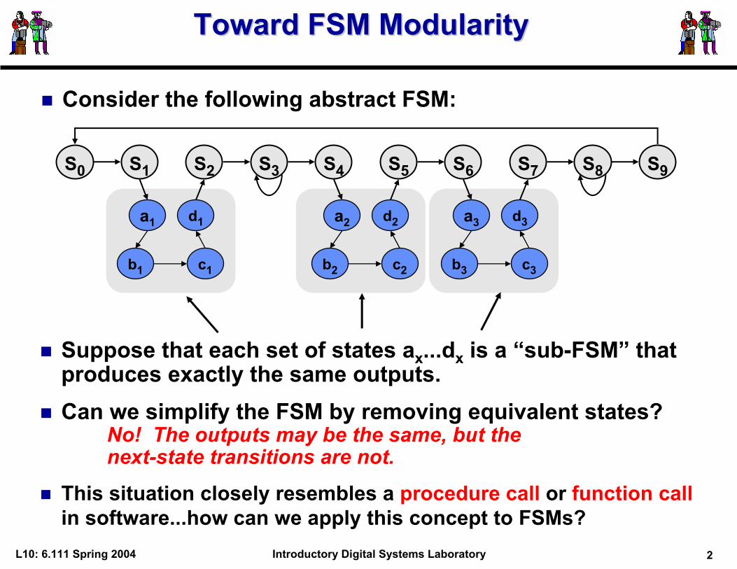
� Consider the following abstract FSM:
S0
a1
b1 c1
d1
S1 S2 S3 S4 S5 S6 S7 S8 S9
a2
b2 c2
d2 a3
b3 c3
d3
� Suppose that each set of states ax...dx is a “sub-FSM” that produces exactly the same outputs.
� Can we simplify the FSM by removing equivalent states?No! The outputs may be the same, but thenext-state transitions are not.
� This situation closely resembles a procedure call or function call in software...how can we apply this concept to FSMs?
L10: 6.111 Spring 2004 Introductory Digital Systems Laboratory 2
The Major/Minor FSM AbstractionThe Major/Minor FSM Abstraction
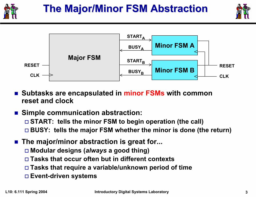
Major FSM
Minor FSM A
Minor FSM B
STARTA
STARTB
BUSYA
BUSYBCLK
RESET RESET
CLK
� Subtasks are encapsulated in minor FSMs with common reset and clock
� Simple communication abstraction: � START: tells the minor FSM to begin operation (the call) � BUSY: tells the major FSM whether the minor is done (the return)
� The major/minor abstraction is great for... � Modular designs (always a good thing) � Tasks that occur often but in different contexts � Tasks that require a variable/unknown period of time � Event-driven systems
L10: 6.111 Spring 2004 Introductory Digital Systems Laboratory 3
Inside the Major FSMInside the Major FSM
S1 S2
START S3 S4...
BUSYBUSY
BUSY
BUSY
BUSY BUSY
1. Wait until the minor FSM
is ready
2. Trigger the minor FSM
(and make sure it’s started)
3. Wait until the minor FSM
is done
START
BUSY
Major FSMState S1 S2 S2 S3 S3 S3 S4
CLK
L10: 6.111 Spring 2004 Introductory Digital Systems Laboratory 4
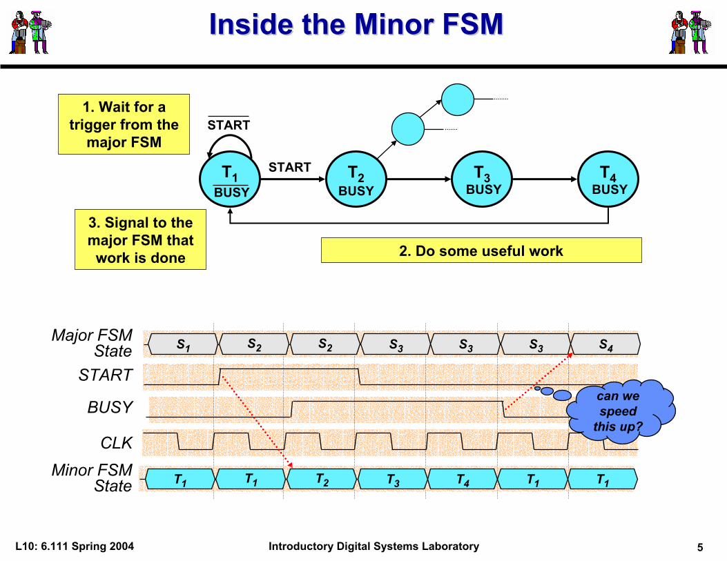
Inside the Minor FSMInside the Minor FSM
T2 BUSY
T3 BUSY
T4 BUSY
1. Wait for a trigger from the
major FSM
2. Do some useful work
T1 BUSY
START
START
START
BUSY
Major FSMState S1 S2 S2 S3 S3 S3 S4
CLK Minor FSM
State T1 T1 T2 T3 T4 T1 T1
3. Signal to the major FSM that
work is done
can we speed
this up?
L10: 6.111 Spring 2004 Introductory Digital Systems Laboratory 5
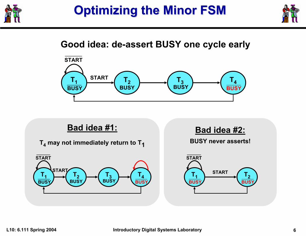
Optimizing the Minor FSMOptimizing the Minor FSM
Good idea: de-assert BUSY one cycle early START
T2 BUSY
T3 BUSY
T4 BUSY
T1 BUSY
START
Bad idea #1: T4 may not immediately return to T1
T2 BUSY
T3 BUSY
T1 BUSY
START
START T4
BUSY
Bad idea #2: BUSY never asserts!
T1 BUSY
START
START T2 BUSY
L10: 6.111 Spring 2004 Introductory Digital Systems Laboratory 6
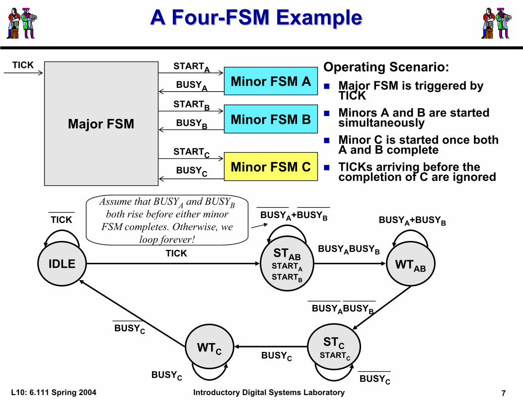
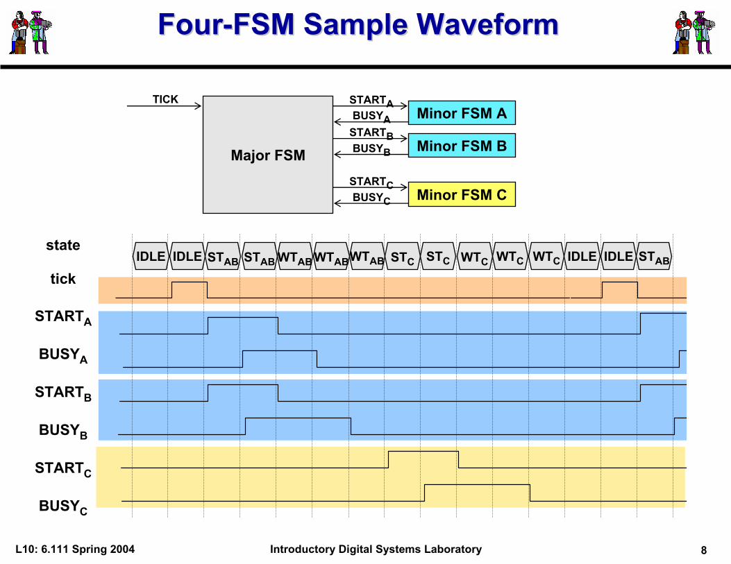
A FourA Four--FSM ExampleFSM Example
Major FSM
Minor FSM A
Minor FSM B
STARTA
STARTB
BUSYA
BUSYB
Minor FSM C STARTC
BUSYC
TICK Operating Scenario: � Major FSM is triggered by
TICK � Minors A and B are started
simultaneously � Minor C is started once both
A and B complete � TICKs arriving before the
completion of C are ignored
IDLE STAB STARTA STARTB
WTAB
TICK BUSYABUSYB
TICK BUSYA+BUSYB BUSYA+BUSYB
STC STARTC
BUSYABUSYB
BUSYC
WTC BUSYC
BUSYC
BUSYC
Assume that BUSYA and BUSYB both rise before either minor
FSM completes. Otherwise, we loop forever!
L10: 6.111 Spring 2004 Introductory Digital Systems Laboratory 7
L10: 6.111 Spring 2004 Introductory Digital Systems Laboratory 8
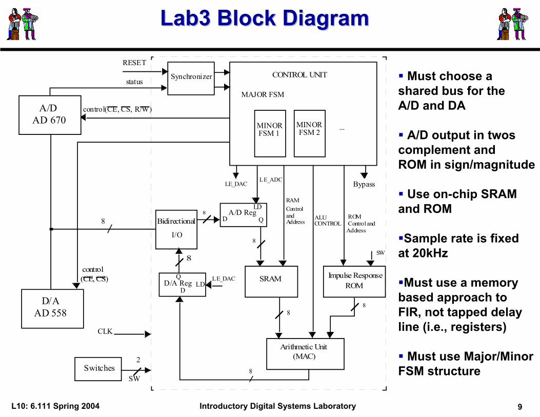
Lab3 Block DiagramLab3 Block Diagram
D/A AD 558
A/D AD 670
status
control(CE, CS, R/W)
MAJOR FSM
MINOR FSM 1
MINOR FSM 2
...
Synchronizer
Bidirectional
I/O
8
SRAM
Arithmetic Unit
CONTROL UNIT
D/A Reg
A/D Reg
L E_ADC Bypass
LE_DAC
LE_DAC
8
ROM
8 8
ALU CONTROL
RAM Control
8
8
control (CE, CS)
SW
2 Switches
SW
RESET
CLK
Impulse Response ROM
(MAC)
LD
D Q
LD D
Q
and Address Control and
Address
8
� Must choose a shared bus for the A/D and DA
� A/D output in twos complement and ROM in sign/magnitude
� Use on-chip SRAM and ROM
�Sample rate is fixed at 20kHz
�Must use a memory based approach to FIR, not tapped delay line (i.e., registers)
� Must use Major/Minor FSM structure
L10: 6.111 Spring 2004 Introductory Digital Systems Laboratory 9
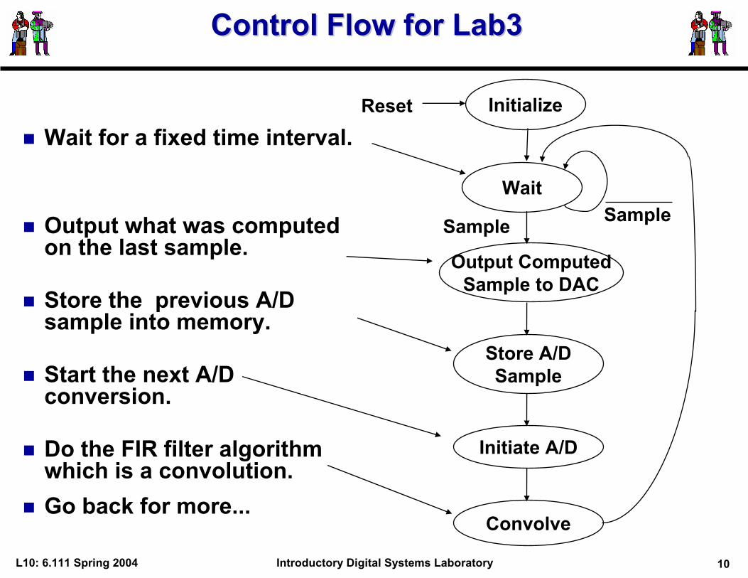
Control Flow for Lab3Control Flow for Lab3
Reset Initialize
� Wait for a fixed time interval.
Wait
� Output what was computed Sample Sample
on the last sample. Output Computed
� Store the previous A/D Sample to DAC
sample into memory. Store A/D
� Start the next A/D Sampleconversion.
� Do the FIR filter algorithm Initiate A/Dwhich is a convolution.
� Go back for more... Convolve
L10: 6.111 Spring 2004 Introductory Digital Systems Laboratory 10
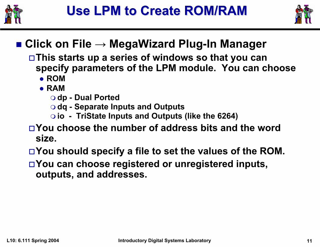
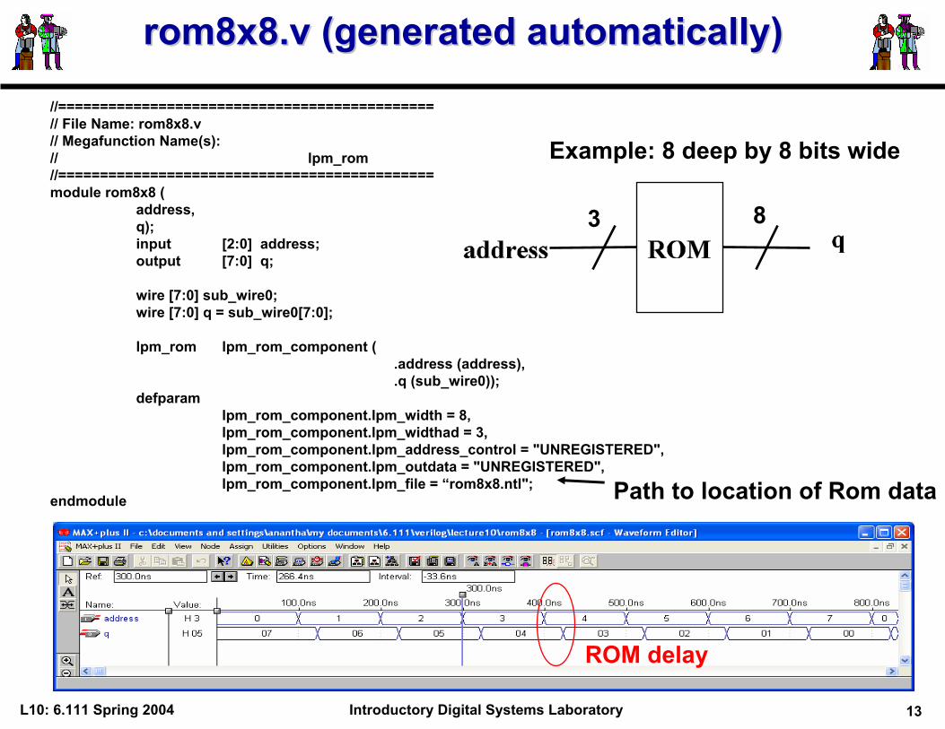
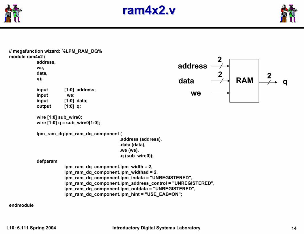
Use LPM to Create ROM/RAMUse LPM to Create ROM/RAM
� Click on File → MegaWizard Plug-In Manager� This starts up a series of windows so that you can
specify parameters of the LPM module. You can choose z ROM z RAM � dp - Dual Ported � dq - Separate Inputs and Outputs � io - TriState Inputs and Outputs (like the 6264)
� You choose the number of address bits and the word size. � You should specify a file to set the values of the ROM.� You can choose registered or unregistered inputs,
outputs, and addresses.
L10: 6.111 Spring 2004 Introductory Digital Systems Laboratory 11
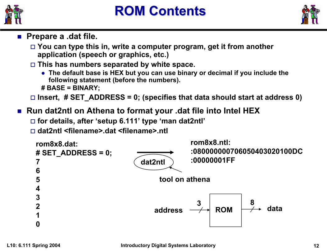
ROM ContentsROM Contents
� Prepare a .dat file. � You can type this in, write a computer program, get it from another
application (speech or graphics, etc.)� This has numbers separated by white space.
z The default base is HEX but you can use binary or decimal if you include the following statement (before the numbers).
# BASE = BINARY;� Insert, # SET_ADDRESS = 0; (specifies that data should start at address 0)
� Run dat2ntl on Athena to format your .dat file into Intel HEX � for details, after ‘setup 6.111’ type ‘man dat2ntl’ � dat2ntl <filename>.dat <filename>.ntl
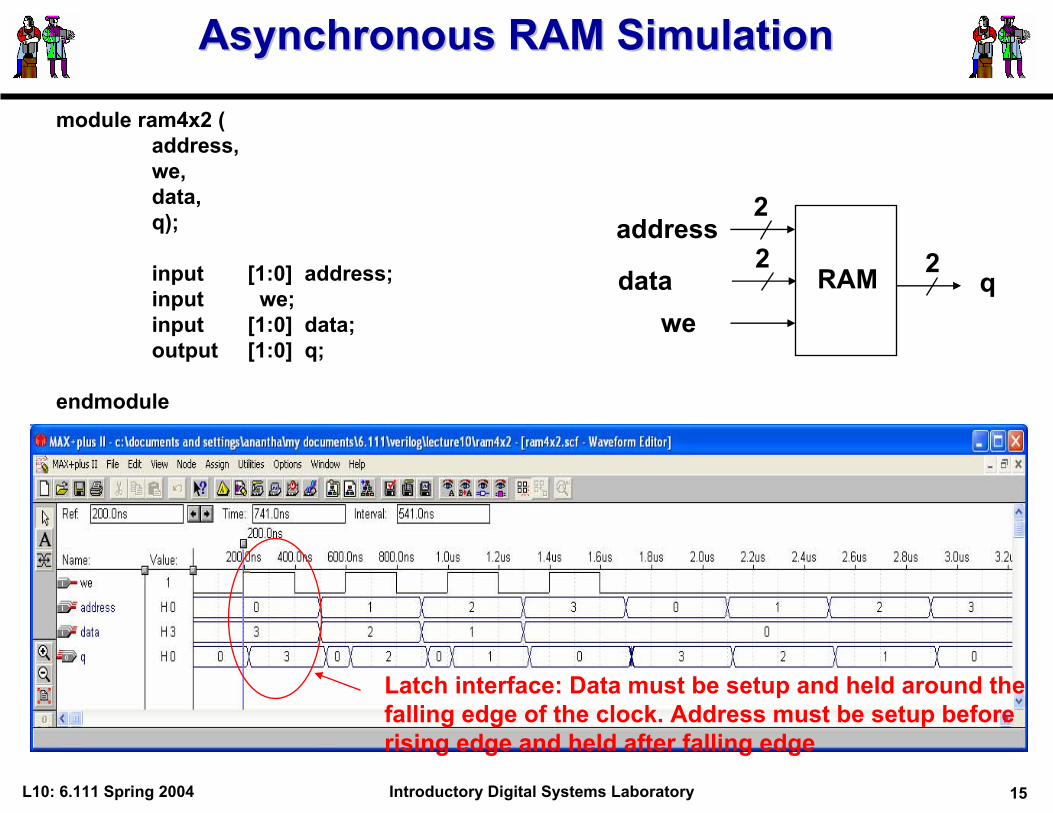
Latch interface: Data must be setup and held around the falling edge of the clock. Address must be setup before rising edge and held after falling edge
L10: 6.111 Spring 2004 Introductory Digital Systems Laboratory 15
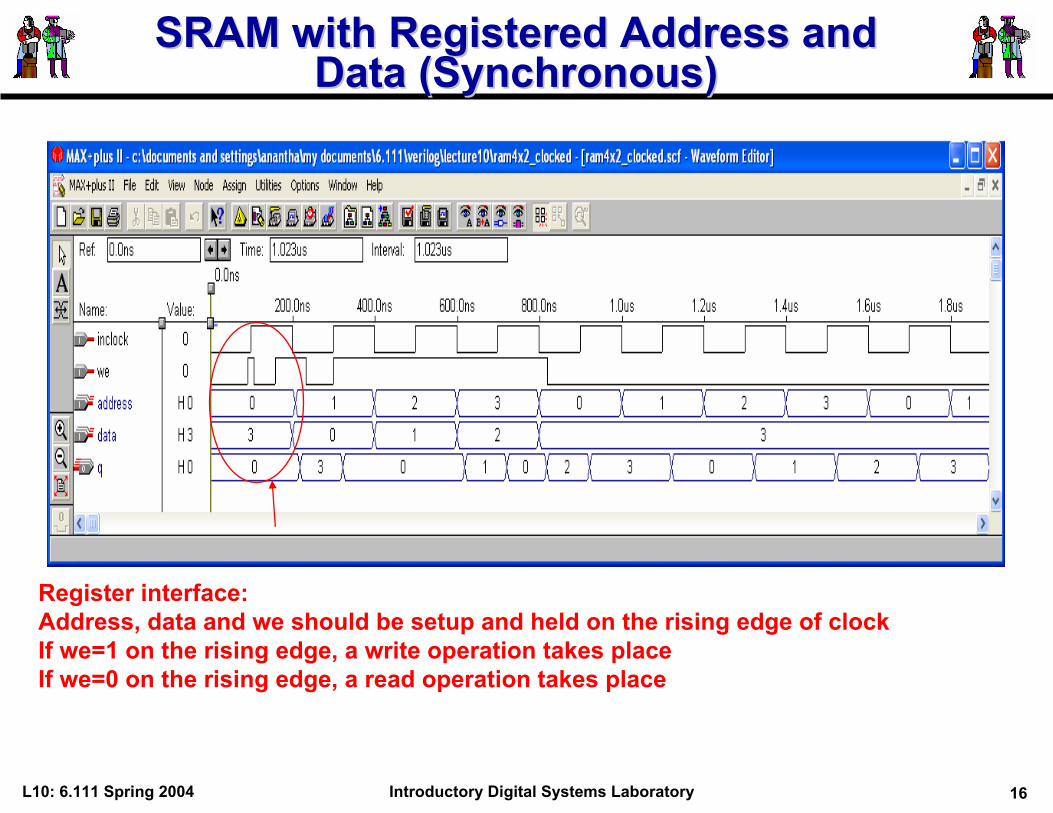
SRAM with Registered Address andSRAM with Registered Address andData (Synchronous)Data (Synchronous)
Register interface: Address, data and we should be setup and held on the rising edge of clock If we=1 on the rising edge, a write operation takes place If we=0 on the rising edge, a read operation takes place
L10: 6.111 Spring 2004 Introductory Digital Systems Laboratory 16


![ANIMAL - mwit.ac.thbio/Resource/BiodiverPDF/8_animal_1_2018.pdf · Porifera [Major] Cnidaria [Major] Ctenophore [Minor] Platyhelminthes [Major] Rotifera [Minor] Nematoda [Major] Annelida](https://static.documents.pub/doc/80x56/5e6b41ee0a650825432d21fa/animal-mwitacth-bioresourcebiodiverpdf8animal12018pdf-porifera-major.jpg)


