17
EE-321 N Lecture-12 UJT (Unijunction Transistor) & UJT Based Triggering Circuit
| Date post: | 13-Feb-2017 |
| Category: |
Engineering |
| Upload: | mohammad-umar-rehman |
| View: | 924 times |
| Download: | 6 times |

EE-321 N
Lecture-12
UJT (Unijunction Transistor)
&
UJT Based Triggering Circuit
Introduction
• Three terminal single junction latching device*
• Different from either diode (due to 3 terminals) or the transistor (can’t amplify)
• Wide range of applications like oscillators, trigger circuits, sawtooth generators, phase control
• Overcomes the limitations of previous trigger circuits like power dissipation & high dependability on the SCR chatacteristics
• Other variants include CUJT & PUT
31-Oct-12 EE-321N, Lec-12 2

Structure & Symbol
E
B2
B1B1
A
B2
E
RB2
RB1n-type
p-type
Eta-point
Basic Structure Symbol
31-Oct-12 3 EE-321N, Lec-12
Equivalent Circuit
RB2
VBB
+
-
E
B1
RB1 VBB
A+
-
Ve Ie
B2
Eta-point
V1
VD
Equivalent Circuit of UJT31-Oct-12 4 EE-321N, Lec-12
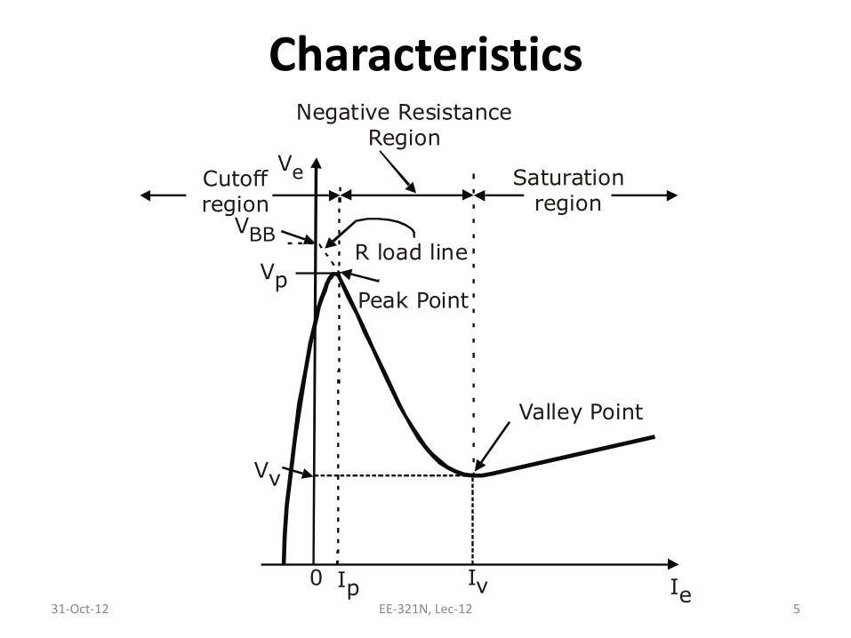
Characteristics
31-Oct-12 5 EE-321N, Lec-12
Ve
VBBR load line
Vp
Vv
IeIvIp0
Peak Point
Cutoffregion
Negative ResistanceRegion
Saturation region
Valley Point

Device Description & Operation
• Consists of a lightly doped n-type Si base to which heavily doped p-type emitter is embedded
• At the two ends, there are ohmic contacts designated as Base 1 & Base 2
• Thus the 3 terminals are: E, B1 & B2
• An interbase resistance RBB = RB1 + RB2|IE = 0
(~5-10 kΩ) exists between the two bases
31-Oct-12 EE-321N, Lec-12 6

Contd...
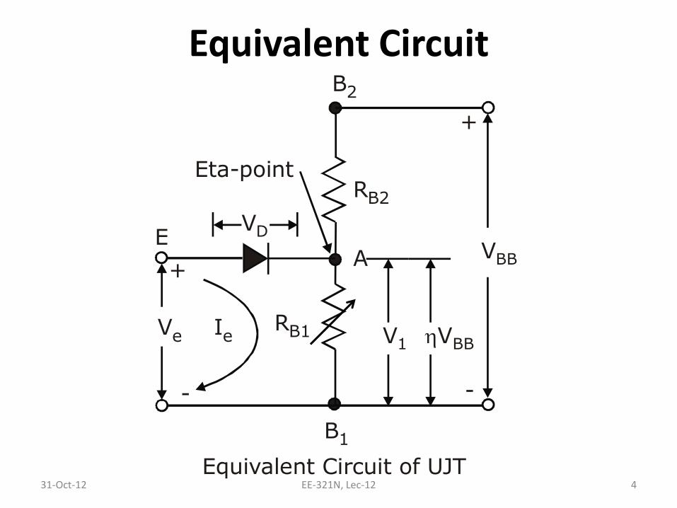
• Equivalent circuit consists of a pn junction diode and the interbase resistance divided into two parts RB1 & RB2
• When a voltage VBB is applied between the bases, the potential of point A w. r. t. B1 is
31-Oct-12 EE-321N, Lec-12 7
1 11
1 2
B BAB BB BB BB
B B BB
R RV V V V
R R R

Contd...
• Where, is known as intrinsic stand off ratio & ranges from 0.5-0.8
• When VE < V1, the equivalent diode is R. B. This is the OFF state of the device & is shown as very low current region on the VE-IE curve
• When VE > V1 + VD, the diode becomes F. B. this is the ON state of the device
• Vp = V1 + VD = VBB + VD is known as the peak point voltage
31-Oct-12 EE-321N, Lec-12 8
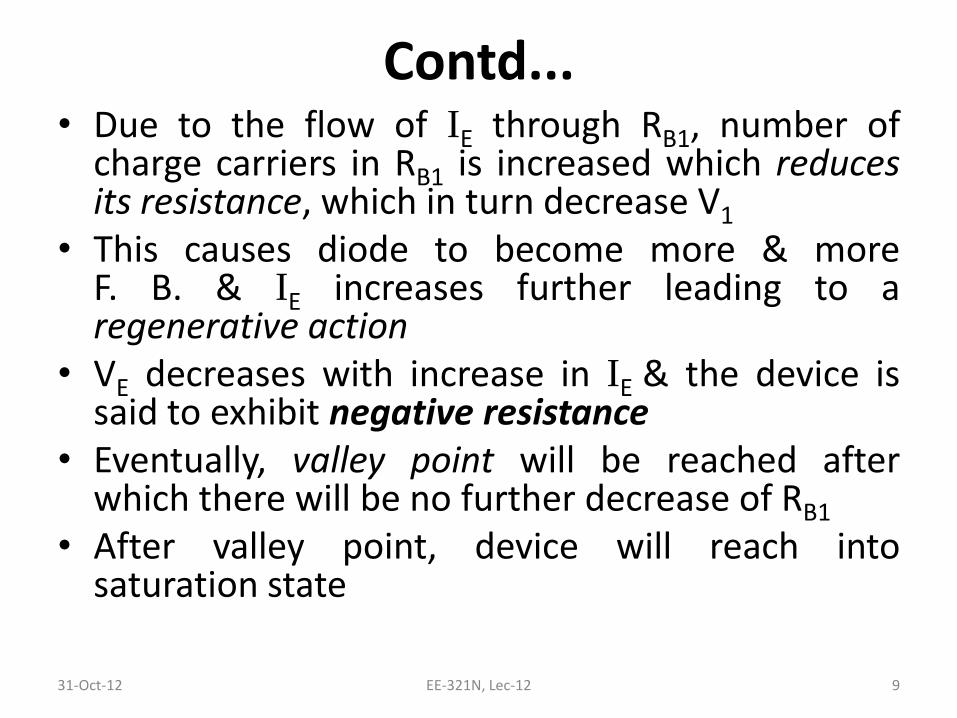
Contd... • Due to the flow of IE through RB1, number of
charge carriers in RB1 is increased which reduces its resistance, which in turn decrease V1
• This causes diode to become more & more F. B. & IE increases further leading to a regenerative action
• VE decreases with increase in IE & the device is said to exhibit negative resistance
• Eventually, valley point will be reached after which there will be no further decrease of RB1
• After valley point, device will reach into saturation state 31-Oct-12 EE-321N, Lec-12 9

UJT Relaxation Oscillator
31-Oct-12 EE-321N, Lec-12 10
R R2
VBB
R1C
EB2
B1Ve vo
Ve
Vp
VV
Vo
t
t
Capacitorcharging
1=RC
T
V +VBB
VP
2 1=R C
Capacitordischarging
Vv

Contd...
• The –ve resistance region of the UJT can be used to advantage in relaxation oscillator which can provide triggering pulses for SCR
• In the above ckt, R1 & R2 are chosen to be much smaller than the interbase resistances
• The charging resistance R should be such that its load line passes through the device characteristics in the negative resistance region
31-Oct-12 EE-321N, Lec-12 11

Contd... • When a source voltage VBB is applied to it, C
begins to charge through R exponentially towards VBB according to the equation
• When vC reaches the peak point voltage, E-B1 junction breaks down & the UJT turns ON. Now C discharges rapidly through R1
• 2 << 1
• UJT turns OFF when the voltage decays to valley voltage Vv
31-Oct-12 EE-321N, Lec-12 12
/1 t RC
C BBv V e
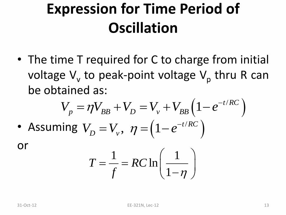
Expression for Time Period of Oscillation
• The time T required for C to charge from initial voltage Vv to peak-point voltage Vp thru R can be obtained as:
• Assuming
or
31-Oct-12 EE-321N, Lec-12 13
/1 t RC
p BB D v BBV V V V V e
/, 1 t RC
D vV V e
1 1ln
1T RC
f

Contd...
• If T is taken as the time pd. of the O/P pulse duration (neglecting small discharge time), then firing angle is given by
• Design considerations include selection of R1, R2 & R
31-Oct-12 EE-321N, Lec-12 14
1ln
1T RC
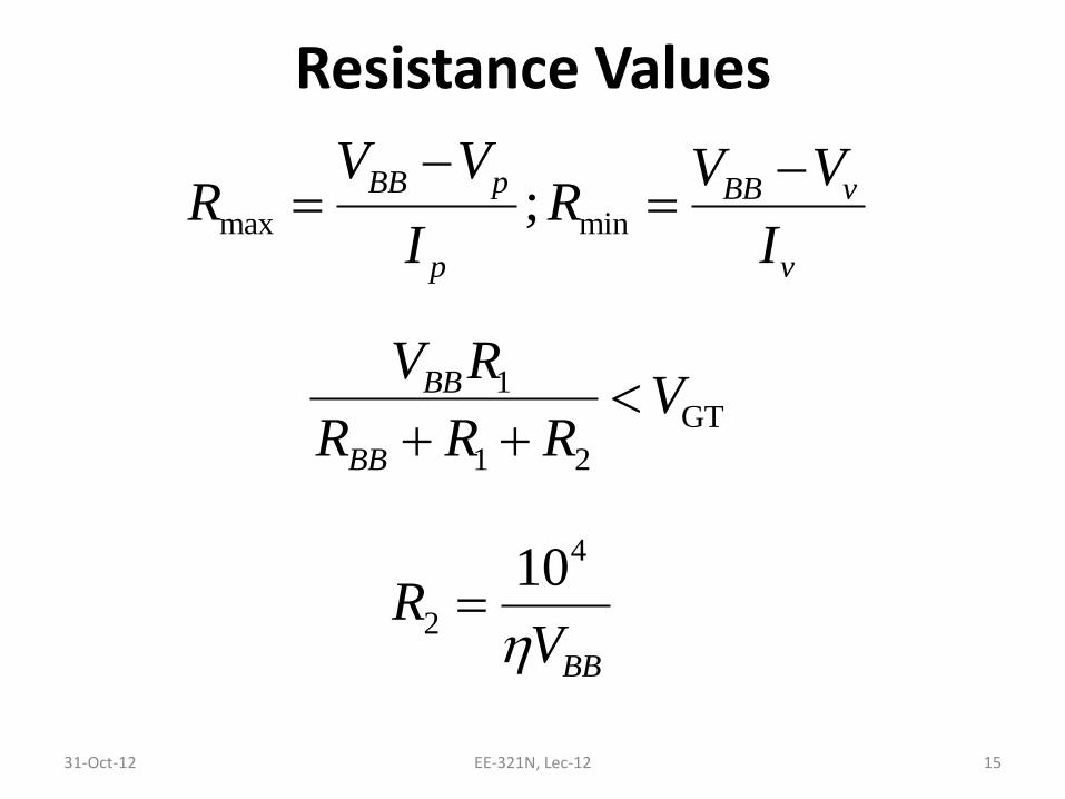
Resistance Values
31-Oct-12 EE-321N, Lec-12 15
max min;BB p BB v
p v
V V V VR R
I I
1GT
1 2
BB
BB
V RV
R R R
4
2
10
BB
RV

Further Resources
1. Video lectures on “Basic Electronics & Lab”, Prof. T. S. Natarajan, Lec-34 UJT
Available on www.nptel.iitm.ac.in,
www.youtube.com/iit
2. Boylestad & Nashelsky, “Electronic Devices & Circuit Theory”, 7/e, PHI
31-Oct-12 16 EE-321N, Lec-12
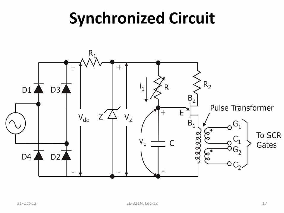
Synchronized Circuit
31-Oct-12 EE-321N, Lec-12 17
R
C
+
-
D1 D3
D4 D2
Vdc
R1
VZ
+
-
Z
i1
vc
+
-
R2
G1
C1
G2
C2
Pulse TransformerE
B2
B1
To SCR
Gates


