L15: 6.111 Spring 2008 1 Introductory Digital Systems Laboratory L15: VLSI Integration and Performance L15: VLSI Integration and Performance Transformations Transformations Acknowledgements: • Lecture prepared by Professor Anantha Chandrakasan • Lecture material adapted from J. Rabaey, A. Chandrakasan, B. Nikolic, “Digital Integrated Circuits: A Design Perspective” Copyright 2003 Prentice Hall/Pearson. • Curt Schurgers • Moore’s Law and Integration • IC Design ¾ ASIC Design ¾ Clocks ¾ Test • Performance Transformations • Trends
Transcript
L15: 6.111 Spring 2008 1Introductory Digital Systems Laboratory
L15: VLSI Integration and Performance L15: VLSI Integration and Performance TransformationsTransformations
Acknowledgements: • Lecture prepared by Professor Anantha Chandrakasan• Lecture material adapted from J. Rabaey, A. Chandrakasan, B. Nikolic, “Digital
L15: 6.111 Spring 2008 3Introductory Digital Systems Laboratory
MooreMoore’’s Laws Law
In 1965, Gordon Moore was preparing a speech and made a memorable observation. When he started to graph data about the growth in memory chip performance, he realized there was a striking trend. Each new chip contained roughly twice as much capacity as its predecessor, and each chip was released within 18-24 months of the previous chip. If this trend continued, he reasoned, computing power would rise exponentially over relatively brief periods of time.
“…E.O. Wilson, the famous Harvard biologist who is an expert on ants, estimates that there are 10 to the 16th and 10 to the 17th ants on earth. But if you look at this curve, this year we’re making one transistor for every ant.” – Gordon Moore, “An Update on Moore’s Law”
Gordon Moore, KeynotePresentation at ISSCC 2003
40048008
80808085 8086
286386
486Pentium® proc
P6
0.001
0.01
0.1
1
10
100
1000
1970 1980 1990 2000 2010Year
Tran
sist
ors
(MT)
2X growth in 1.96 years!
Courtesy of S. Borkar (Intel)
L15: 6.111 Spring 2008 4Introductory Digital Systems Laboratory
Evolution of Transistor IntegrationEvolution of Transistor Integration
Moore’s Law: transistor density doubles every 1.5 - 2 years
1970 1974 1978 1982 1986 1990 1994 1998 2002
1K
4K16K
64K
1M
4M
16M
128MDRAMCost / Bit ($, 95)
2006
256M 1G
4004
8086
8080
Pentium Pro
8028680386
Pentium
Pentium IIPentium III
Cos
t/Bit
($, 9
5)
10-1
10-2
10-3
10-4
10-5
10-6
10-7
10-8
Tran
sist
ors
/ Chi
p
107
106
105
104
103
108
109
Cos
t/Fun
ctio
n
Pentium IV
#1
256K80486
64M
#2
Microprocessor
102
10-9
L15: 6.111 Spring 2008 5Introductory Digital Systems Laboratory
Layout 101Layout 101
N-channel P-channel
GND
VDD
meta pol p+
contact frommet to ndiff
L
W
L
W
I OU
n-type
p-type
metal/pdi contact
n+
I OU
VDD
SG
D
D
SG
3-D Cross-Section
Circuit Representation
Layout
Follow simple design rules (contractbetween process and circuit designers)
L15: 6.111 Spring 2008 6Introductory Digital Systems Laboratory
Custom Design/LayoutCustom Design/Layout
Adder stage 1
Wiring
Adder stage 2
Wiring
Adder stage 3B
it slice 0
Bit slice 2
Bit slice 1
Bit slice 63
Sum Select
Shifter
Multiplexers
Loopback Bus
From register files / Cache / Bypass
To register files / Cache
Loopback Bus
Loopback Bus
Die photograph of the Die photograph of the Itanium integer Itanium integer datapathdatapath
Hand crafting the layout to achieve maximum clock rates (> 1Ghz)Exploits regularity in datapath structure to optimize interconnects
9-1
Mux
9-1
Mux
5-1
Mux
2-1
Mux
ck1
CARRYGEN
SUMGEN+ LU
1000um
b
s0
s1
g64
sum sumb
LU : LogicalUnit
SUM
SEL
a
to Cache
node1
REG
Itanium has 6 integer execution units like thisItanium has 6 integer execution units like this
L15: 6.111 Spring 2008 7Introductory Digital Systems Laboratory
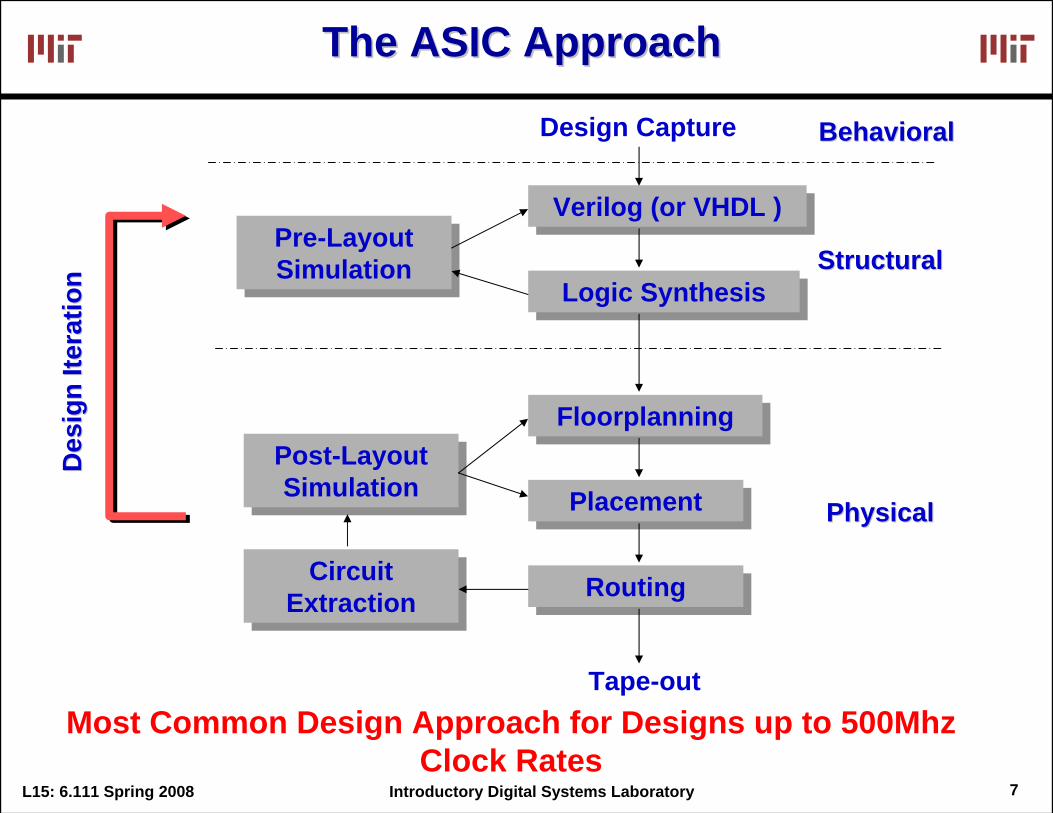
The ASIC ApproachThe ASIC Approach
Verilog (or VHDL )Verilog (or VHDL )
Logic SynthesisLogic Synthesis
FloorplanningFloorplanning
PlacementPlacement
RoutingRouting
Tape-out
Circuit Extraction
Circuit Extraction
Pre-Layout Simulation
Pre-Layout Simulation
Post-Layout Simulation
Post-Layout Simulation
StructuralStructural
PhysicalPhysical
BehavioralBehavioralDesign Capture
Des
ign
Itera
tion
Des
ign
Itera
tion
Most Common Design Approach for Designs up to 500Mhz Clock Rates
L15: 6.111 Spring 2008 8Introductory Digital Systems Laboratory
Standard Cell ExampleStandard Cell Example
3-input NAND cell(from ST Microelectronics):C = Load capacitanceT = input rise/fall time
Power Supply Line (VDD )
Ground Supply Line (GND)
Each library cell (FF, NAND, NOR, INV, etc.) and the variations on size (strength of the gate) is fully characterized across temperature, loading, etc.
Delay in (ns)!!
L15: 6.111 Spring 2008 9Introductory Digital Systems Laboratory
Standard Cell Layout MethodologyStandard Cell Layout Methodology
Cell-structure hidden under interconnect layers
2-level metal technology Current Day Technology
With limited interconnect layers, dedicated routing channels between rows of standard cells are needed
Width of the cell allowed to vary to accommodate complexityInterconnect plays a significant role in speed of a digital circuit
L15: 6.111 Spring 2008 10Introductory Digital Systems Laboratory
L15: 6.111 Spring 2008 13Introductory Digital Systems Laboratory
Analog Circuits: Clock Frequency Analog Circuits: Clock Frequency Multiplication (Phase Locked Loop)Multiplication (Phase Locked Loop)
Courtesy M. PerrottCourtesy M. Perrott
VCO produces high frequency square waveDivider divides down VCO frequencyPFD compares phase of ref and divLoop filter extracts phase error information
Used widely in digital systems for clock synthesis(a standard IP block in most ASIC flows)
PLL
Intel 486, 50Mhz
up
down
L15: 6.111 Spring 2008 14Introductory Digital Systems Laboratory
Scan TestingScan Testing
CLK
shift in ScanShift
shift out
01
ScanShift
shift in
01
ScanShift
... Idea: have a mode in which all registers are chained into one giant shift register which can be loaded/ read-out bit serially. Test remaining (combinational)logic by
(1) in “test” mode, shift in new values for all register bits thus setting up the inputs to the combinational logic
(2) clock the circuit once in “normal” mode, latching the outputs of the combinational logic back into the registers
(3) in “test” mode, shift out the values of all register bits and compare against expected results.
Courtesy of C. Terman and IEEE Press
L15: 6.111 Spring 2008 15Introductory Digital Systems Laboratory
There are a large number of implementations of the same functionality
These implementations present a different point in the area-time-power design space
Behavioral transformations allow exploring the design space a high-level
Optimization metrics:
area
time
power1. Area of the design2. Throughput or sample time TS3. Latency: clock cycles between
the input and associated output change
4. Power consumption5. Energy of executing a task6. …
L15: 6.111 Spring 2008 19Introductory Digital Systems Laboratory
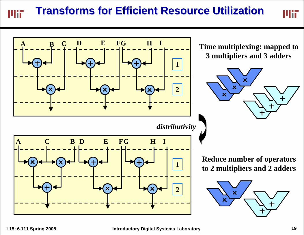
Transforms for Efficient Resource UtilizationTransforms for Efficient Resource Utilization
CA B FD E
2
1
IG H
2
1
CA B
distributivity
Time multiplexing: mapped to 3 multipliers and 3 adders
Reduce number of operators to 2 multipliers and 2 adders
FD E IG H
L15: 6.111 Spring 2008 20Introductory Digital Systems Laboratory
A Very Useful Transform: RetimingA Very Useful Transform: Retiming
Retiming is the action of moving delay around in the systemsDelays have to be moved from ALL inputs to ALL outputs or vice versa
D
D
D
D
D
Cutset retiming: A cutset intersects the edges, such that this would result in two disjoint partitions of these edges being cut. To retime, delays are moved from the ingoing to the outgoing edges or vice versa.
Benefits of retiming:• Modify critical path delay• Reduce total number of registers
D
D
D
L15: 6.111 Spring 2008 21Introductory Digital Systems Laboratory
Retiming Example: FIR FilterRetiming Example: FIR Filter
associativity of the addition
D D Dx(n)
h(0) h(1) h(2) h(3)
y(n)
D D Dx(n)
h(0) h(1) h(2) h(3)
y(n)
D D D
x(n)
h(0) h(1) h(2) h(3)
y(n)
retime
Direct form
Transposed form
Symbol for multiplication
∑=
⋅−=⊗=K
i
ihinxnxnhny0
)()()()()(
(10)
(4)
Tclk = 22 ns
Tclk = 14 ns
Note: here we use a first cut analysis that assumes the delay of a chain of operators is the sum of their individual delays. This is not accurate.
L15: 6.111 Spring 2008 22Introductory Digital Systems Laboratory
Pipelining, Just Another TransformationPipelining, Just Another Transformation (Pipelining = Adding Delays + Retiming)(Pipelining = Adding Delays + Retiming)
How to pipeline:1. Add extra registers at
all inputs2. Retime
D
D
D
D
D
D
D
D
D
retime
add input registers
Contrary to retiming, pipelining adds extra registers to the system
L15: 6.111 Spring 2008 23Introductory Digital Systems Laboratory
The Power of Transforms: The Power of Transforms: LookaheadLookahead
D
x(n) y(n)
A
2D
x(n) y(n)
D AA
2D
x(n) y(n)
DAAA
2D
x(n) y(n)
DA2A
D
x(n) y(n)
A2
A DD
loop unrolling
distributivity
associativity
retiming
precomputed
y(n) = x(n) + A[x(n-1) + A y(n-2)]
y(n) = x(n) + A y(n-1)
Try pipeliningthis structure
How about pipeliningthis structure!
L15: 6.111 Spring 2008 24Introductory Digital Systems Laboratory
Key Concern in Modern VLSI: Variations!Key Concern in Modern VLSI: Variations!
10
100
1000
10000
1000 500 250 130 65 32
Technology Node (nm)
Mea
n N
umbe
r of
Dop
ant
Ato
ms
Random Dopant Fluctuations40
50
60
70
80
90
100
110
Tem
pera
ture
(C)
Temp Variation & Hot spots
ToxD
GATE
SOURCE DRAIN
Leff
BODY
DelayDelay
Path DelayPath Delay Prob
abili
tyPr
obab
ility Due to Due to
variations in:variations in:VVdddd , V, Vtt , and , and
TempTemp
Deterministic design techniques inadequate in the futureDeterministic design techniques inadequate in the futureDeterministic design techniques inadequate in the futureCourtesy of S. Borkar (Intel)
With 100b transistors, 1b unusable (variations)
L15: 6.111 Spring 2008 25Introductory Digital Systems Laboratory
Trends: Trends: ““Chip in a DayChip in a Day”” ((Matlab/SimulinkMatlab/Simulink to Siliconto Silicon……))
Mult2
Mac2Mult1 Mac1
S reg X reg Add,Sub,Shift
Courtesy of R. Brodersen
Map algorithms directly to silicon - bypass writing Verilog!
L15: 6.111 Spring 2008 26Introductory Digital Systems Laboratory(courtesy of G. Qu, M. Potkonjak)(courtesy of G. Qu, M. Potkonjak)
Trends: Watermarking of Digital Designs Trends: Watermarking of Digital Designs
Fingerprinting is a technique to deter people from illegally redistributing legally obtained IP by enabling the author of the IP to uniquely identify the original buyer of the resold copy. The essence of the watermarking approach is to encode the author's signature. The selection, encoding, and embedding of the signature must result in minimal performance and storage overhead.
same functionality, same area, same performance watermark of 4768 bits embedded
Presenter
Presentation Notes
Software piracy (www.nopiracy.com) 38% of all software used is illegally copied $11 billion revenue loss in 1998 Hardware piracy $12 billion market on hardware IP by 2002 100 reverse engineering labs (most not public) One of the key problems in SoC design