• Asynchronous I/O performance– Up to asynchronous timing mode 5– tRC/tWC: 20ns (MIN)– Up to asynchronous timing mode 5– Read/write throughput per pin: 50 MT/s
PDF: 09005aef83d2277aL74A_64Gb_128Gb_256Gb_AsyncSync_NAND.pdf Rev. G 1/14 EN 1 Micron Technology, Inc. reserves the right to change products or specifications without notice.
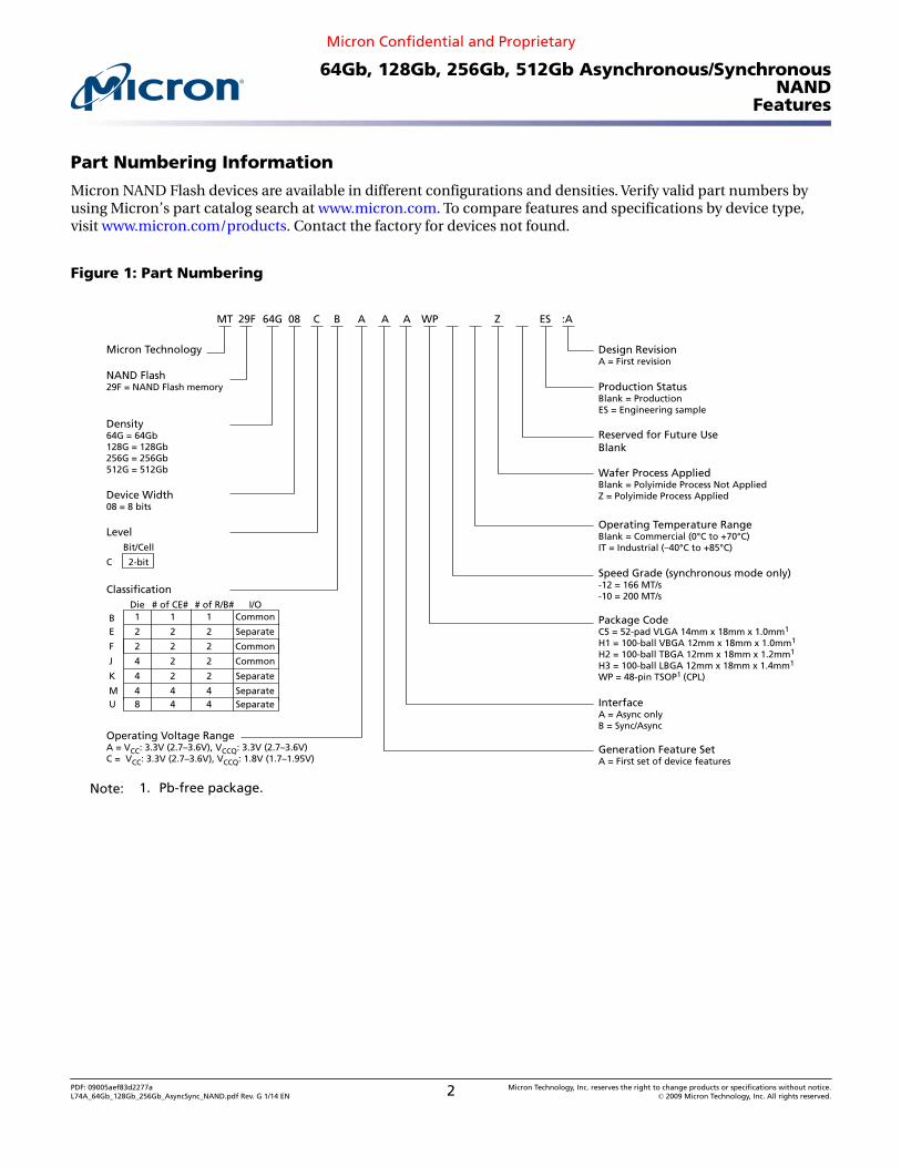
Micron NAND Flash devices are available in different configurations and densities. Verify valid part numbers byusing Micron’s part catalog search at www.micron.com. To compare features and specifications by device type,visit www.micron.com/products. Contact the factory for devices not found.
PDF: 09005aef83d2277aL74A_64Gb_128Gb_256Gb_AsyncSync_NAND.pdf Rev. G 1/14 EN 2 Micron Technology, Inc. reserves the right to change products or specifications without notice.
Identification Operations ................................................................................................................................ 55READ ID (90h) ............................................................................................................................................ 55READ ID Parameter Tables .......................................................................................................................... 56READ PARAMETER PAGE (ECh) .................................................................................................................. 57
Parameter Page Data Structure Tables ..................................................................................................... 58READ UNIQUE ID (EDh) ............................................................................................................................ 69
Configuration Operations ............................................................................................................................... 70SET FEATURES (EFh) .................................................................................................................................. 70GET FEATURES (EEh) ................................................................................................................................. 71
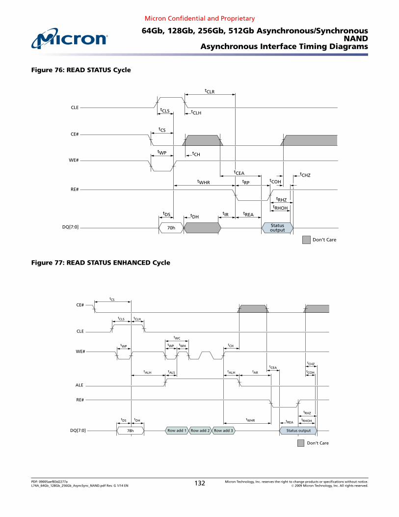
Status Operations ........................................................................................................................................... 75READ STATUS (70h) ................................................................................................................................... 76READ STATUS ENHANCED (78h) ................................................................................................................ 77
PDF: 09005aef83d2277aL74A_64Gb_128Gb_256Gb_AsyncSync_NAND.pdf Rev. G 1/14 EN 3 Micron Technology, Inc. reserves the right to change products or specifications without notice.
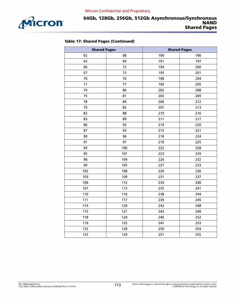
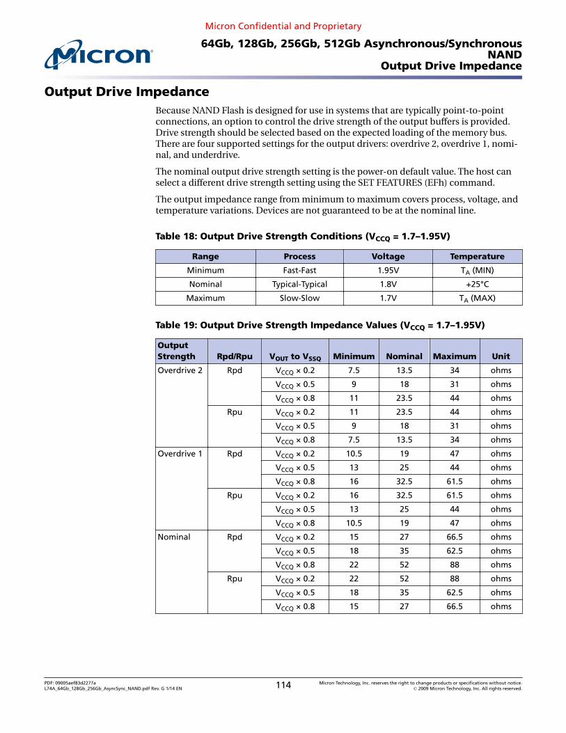
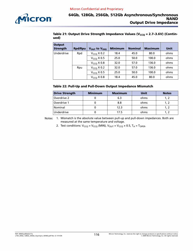
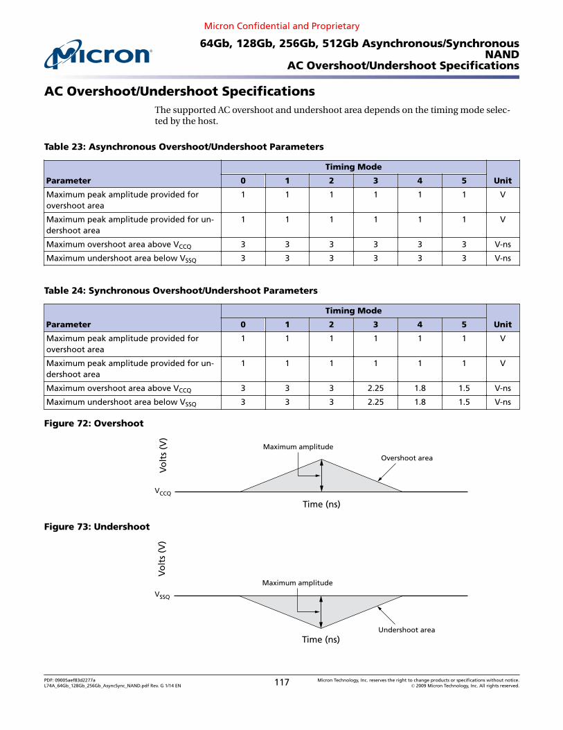
Interleaved Die (Multi-LUN) Operations ......................................................................................................... 110Error Management ........................................................................................................................................ 111Shared Pages ................................................................................................................................................. 112Output Drive Impedance ............................................................................................................................... 114AC Overshoot/Undershoot Specifications ....................................................................................................... 117Synchronous Input Slew Rate ......................................................................................................................... 118Output Slew Rate ........................................................................................................................................... 119Electrical Specifications ................................................................................................................................. 120Electrical Specifications – DC Characteristics and Operating Conditions (Asynchronous) ................................. 122Electrical Specifications – DC Characteristics and Operating Conditions (Synchronous) ................................... 123Electrical Specifications – DC Characteristics and Operating Conditions (VCCQ) ............................................... 123Electrical Specifications – AC Characteristics and Operating Conditions (Asynchronous) ................................. 125Electrical Specifications – AC Characteristics and Operating Conditions (Synchronous) ................................... 127Electrical Specifications – Array Characteristics .............................................................................................. 130Asynchronous Interface Timing Diagrams ...................................................................................................... 131Synchronous Interface Timing Diagrams ........................................................................................................ 142Revision History ............................................................................................................................................ 164
Rev. G Production – 1/14 ............................................................................................................................ 164Rev. F Production – 5/12 ............................................................................................................................ 164Rev. E Production – 3/11 ............................................................................................................................ 164Rev. D Production – 12/10 .......................................................................................................................... 164Rev. C – 7/10 .............................................................................................................................................. 164Rev. B – 2/10 .............................................................................................................................................. 165Rev. A – 11/09 ............................................................................................................................................ 165
PDF: 09005aef83d2277aL74A_64Gb_128Gb_256Gb_AsyncSync_NAND.pdf Rev. G 1/14 EN 4 Micron Technology, Inc. reserves the right to change products or specifications without notice.
PDF: 09005aef83d2277aL74A_64Gb_128Gb_256Gb_AsyncSync_NAND.pdf Rev. G 1/14 EN 5 Micron Technology, Inc. reserves the right to change products or specifications without notice.
PDF: 09005aef83d2277aL74A_64Gb_128Gb_256Gb_AsyncSync_NAND.pdf Rev. G 1/14 EN 6 Micron Technology, Inc. reserves the right to change products or specifications without notice.
PDF: 09005aef83d2277aL74A_64Gb_128Gb_256Gb_AsyncSync_NAND.pdf Rev. G 1/14 EN 7 Micron Technology, Inc. reserves the right to change products or specifications without notice.
PDF: 09005aef83d2277aL74A_64Gb_128Gb_256Gb_AsyncSync_NAND.pdf Rev. G 1/14 EN 8 Micron Technology, Inc. reserves the right to change products or specifications without notice.
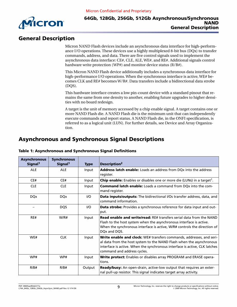
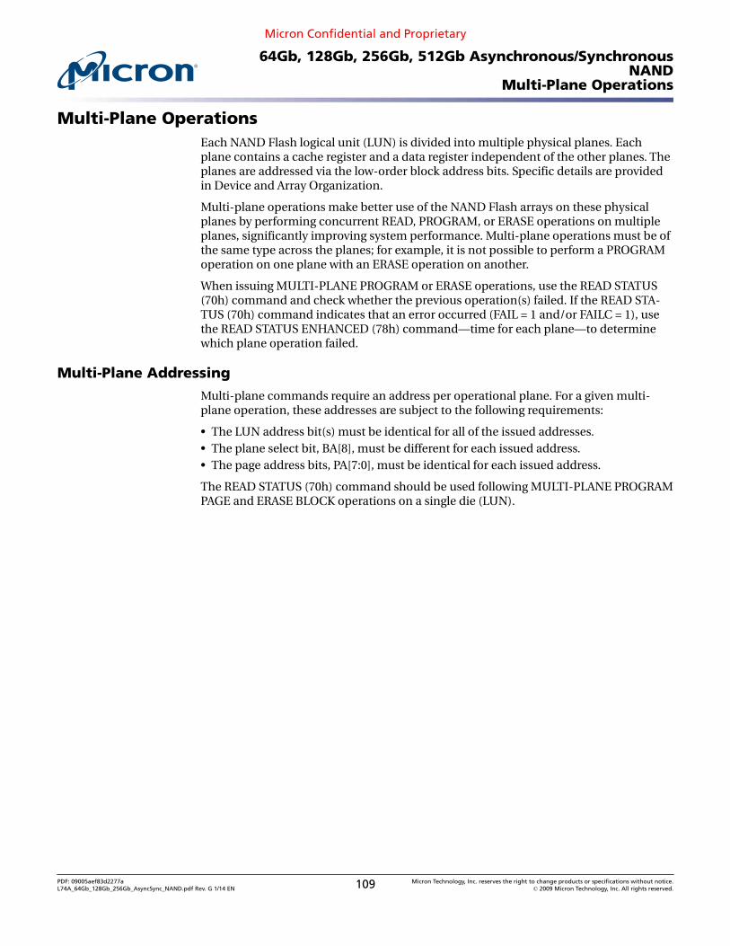
General DescriptionMicron NAND Flash devices include an asynchronous data interface for high-perform-ance I/O operations. These devices use a highly multiplexed 8-bit bus (DQx) to transfercommands, address, and data. There are five control signals used to implement theasynchronous data interface: CE#, CLE, ALE, WE#, and RE#. Additional signals controlhardware write protection (WP#) and monitor device status (R/B#).
This Micron NAND Flash device additionally includes a synchronous data interface forhigh-performance I/O operations. When the synchronous interface is active, WE# be-comes CLK and RE# becomes W/R#. Data transfers include a bidirectional data strobe(DQS).
This hardware interface creates a low pin-count device with a standard pinout that re-mains the same from one density to another, enabling future upgrades to higher densi-ties with no board redesign.
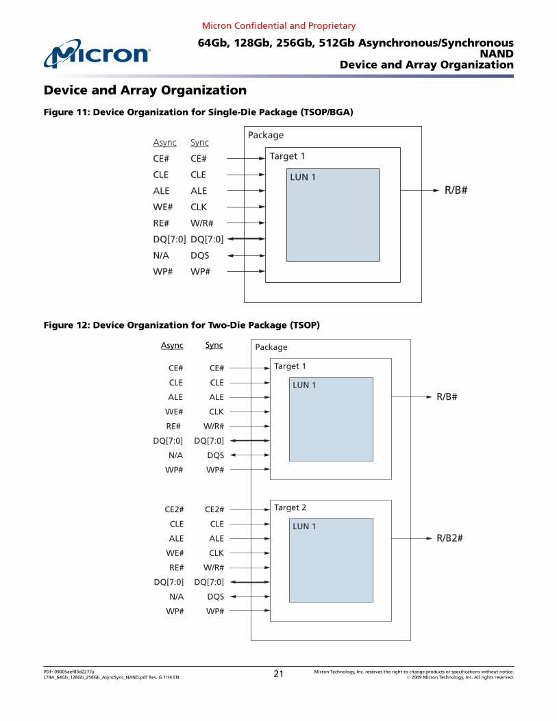
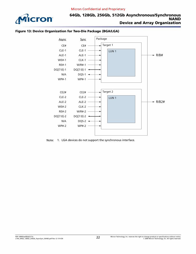
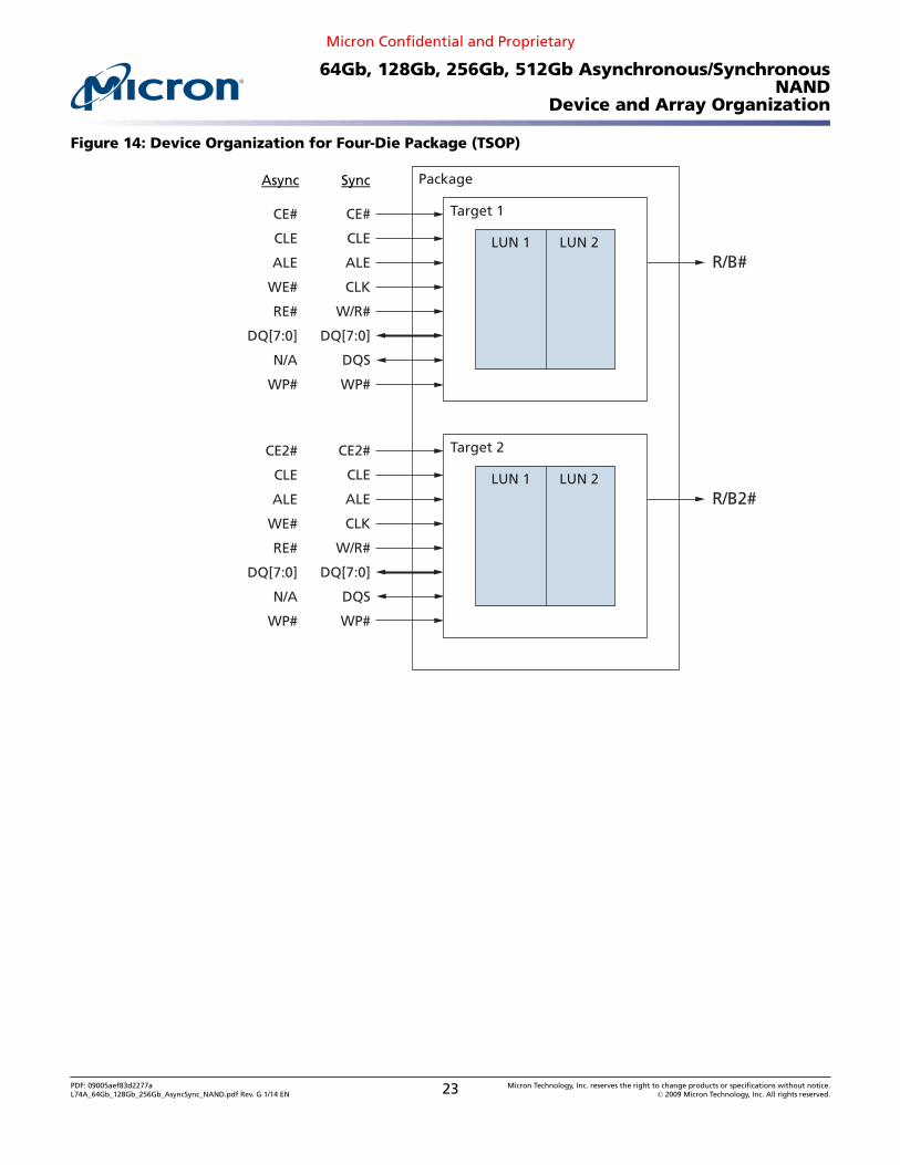
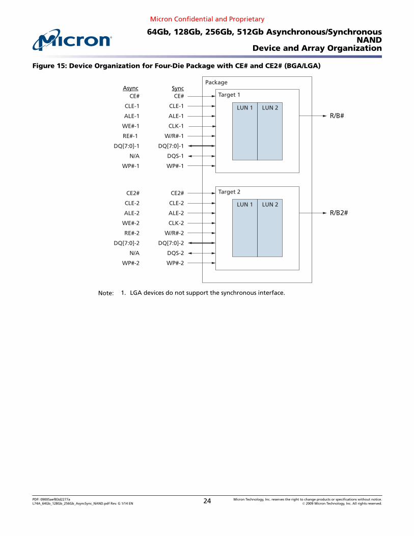
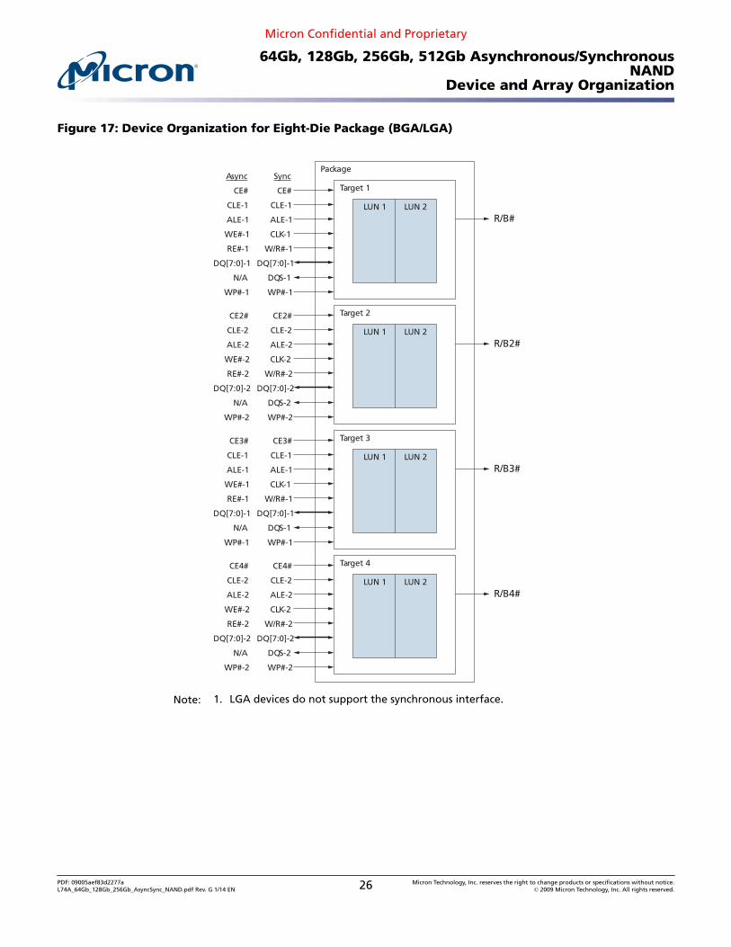
A target is the unit of memory accessed by a chip enable signal. A target contains one ormore NAND Flash die. A NAND Flash die is the minimum unit that can independentlyexecute commands and report status. A NAND Flash die, in the ONFI specification, isreferred to as a logical unit (LUN). For further details, see Device and Array Organiza-tion.
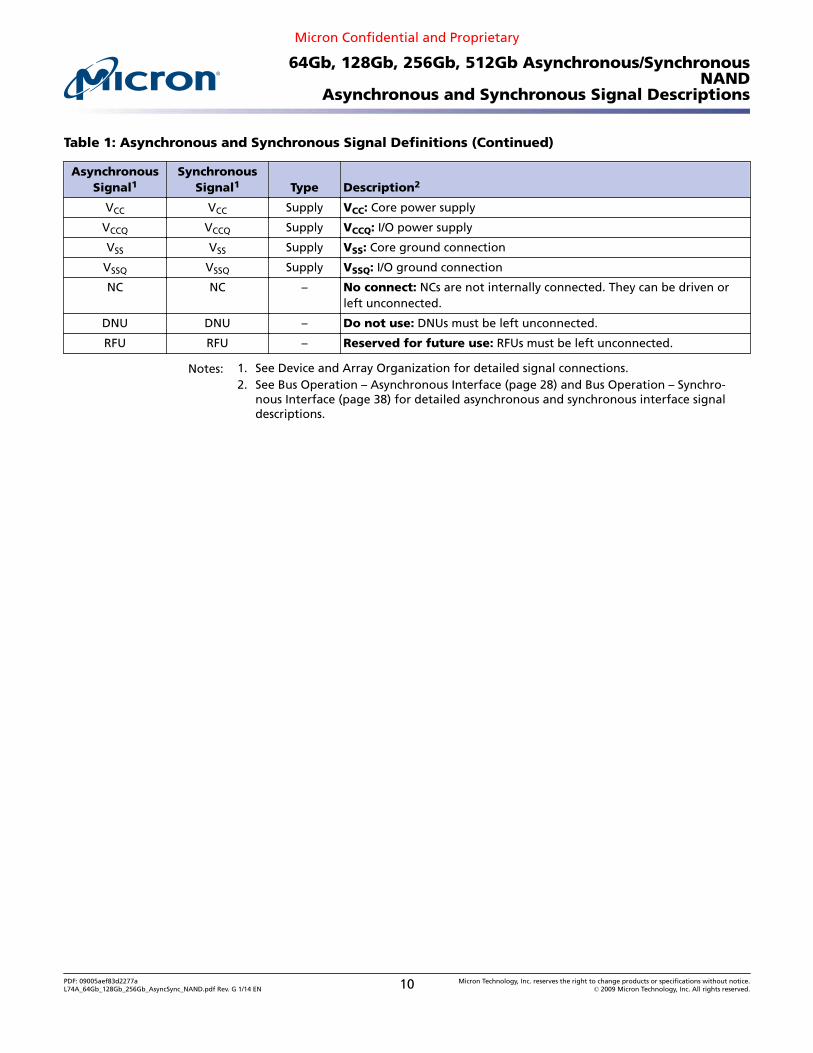
Asynchronous and Synchronous Signal Descriptions
Table 1: Asynchronous and Synchronous Signal Definitions
AsynchronousSignal1
SynchronousSignal1 Type Description2
ALE ALE Input Address latch enable: Loads an address from DQx into the addressregister.
CE# CE# Input Chip enable: Enables or disables one or more die (LUNs) in a target1.
CLE CLE Input Command latch enable: Loads a command from DQx into the com-mand register.
DQx DQx I/O Data inputs/outputs: The bidirectional I/Os transfer address, data, andcommand information.
– DQS I/O Data strobe: Provides a synchronous reference for data input and out-put.
RE# W/R# Input Read enable and write/read: RE# transfers serial data from the NANDFlash to the host system when the asynchronous interface is active.When the synchronous interface is active, W/R# controls the direction ofDQx and DQS.
WE# CLK Input Write enable and clock: WE# transfers commands, addresses, and seri-al data from the host system to the NAND Flash when the asynchronousinterface is active. When the synchronous interface is active, CLK latchescommand and address cycles.
WP# WP# Input Write protect: Enables or disables array PROGRAM and ERASE opera-tions.
R/B# R/B# Output Ready/busy: An open-drain, active-low output that requires an exter-nal pull-up resistor. This signal indicates target array activity.
PDF: 09005aef83d2277aL74A_64Gb_128Gb_256Gb_AsyncSync_NAND.pdf Rev. G 1/14 EN 9 Micron Technology, Inc. reserves the right to change products or specifications without notice.
Table 1: Asynchronous and Synchronous Signal Definitions (Continued)
AsynchronousSignal1
SynchronousSignal1 Type Description2
VCC VCC Supply VCC: Core power supply
VCCQ VCCQ Supply VCCQ: I/O power supply
VSS VSS Supply VSS: Core ground connection
VSSQ VSSQ Supply VSSQ: I/O ground connection
NC NC – No connect: NCs are not internally connected. They can be driven orleft unconnected.
DNU DNU – Do not use: DNUs must be left unconnected.
RFU RFU – Reserved for future use: RFUs must be left unconnected.
Notes: 1. See Device and Array Organization for detailed signal connections.2. See Bus Operation – Asynchronous Interface (page 28) and Bus Operation – Synchro-
nous Interface (page 38) for detailed asynchronous and synchronous interface signaldescriptions.
PDF: 09005aef83d2277aL74A_64Gb_128Gb_256Gb_AsyncSync_NAND.pdf Rev. G 1/14 EN 10 Micron Technology, Inc. reserves the right to change products or specifications without notice.
PDF: 09005aef83d2277aL74A_64Gb_128Gb_256Gb_AsyncSync_NAND.pdf Rev. G 1/14 EN 11 Micron Technology, Inc. reserves the right to change products or specifications without notice.
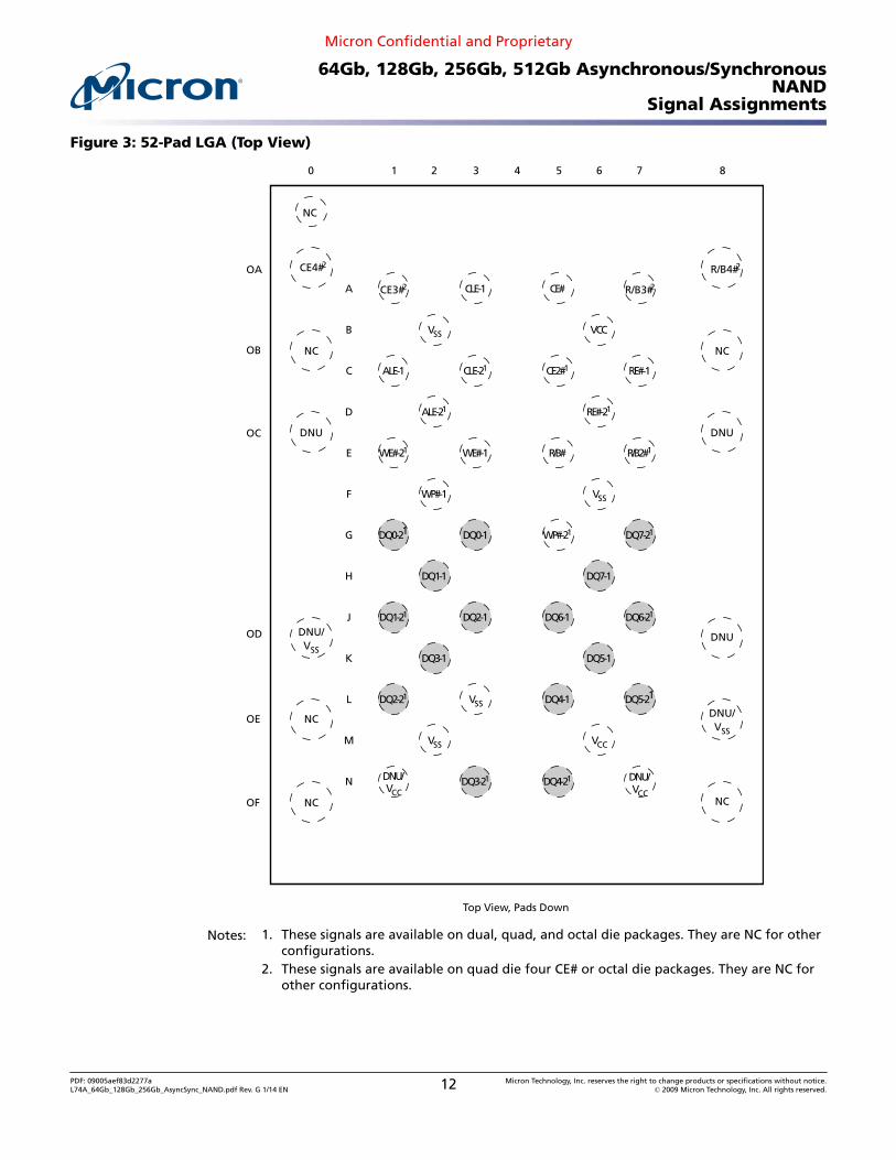
PDF: 09005aef83d2277aL74A_64Gb_128Gb_256Gb_AsyncSync_NAND.pdf Rev. G 1/14 EN 12 Micron Technology, Inc. reserves the right to change products or specifications without notice.
Notes: 1. N/A: This signal is tri-stated when the asynchronous interface is active.2. Signal names in parentheses are the signal names when the synchronous interface is ac-
tive.3. These signals are available on dual, quad, and octal die packages. They are NC for other
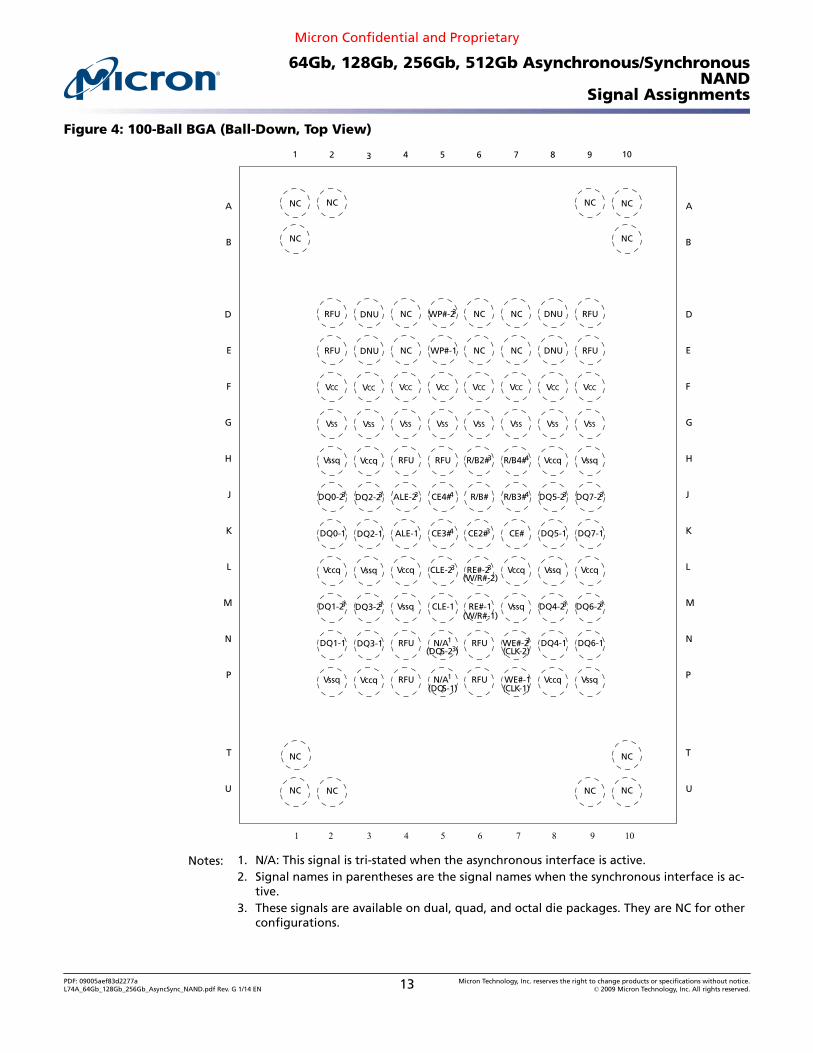
PDF: 09005aef83d2277aL74A_64Gb_128Gb_256Gb_AsyncSync_NAND.pdf Rev. G 1/14 EN 13 Micron Technology, Inc. reserves the right to change products or specifications without notice.
PDF: 09005aef83d2277aL74A_64Gb_128Gb_256Gb_AsyncSync_NAND.pdf Rev. G 1/14 EN 14 Micron Technology, Inc. reserves the right to change products or specifications without notice.
PDF: 09005aef83d2277aL74A_64Gb_128Gb_256Gb_AsyncSync_NAND.pdf Rev. G 1/14 EN 15 Micron Technology, Inc. reserves the right to change products or specifications without notice.
PDF: 09005aef83d2277aL74A_64Gb_128Gb_256Gb_AsyncSync_NAND.pdf Rev. G 1/14 EN 16 Micron Technology, Inc. reserves the right to change products or specifications without notice.
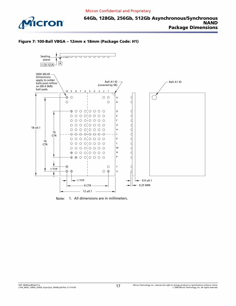
PDF: 09005aef83d2277aL74A_64Gb_128Gb_256Gb_AsyncSync_NAND.pdf Rev. G 1/14 EN 17 Micron Technology, Inc. reserves the right to change products or specifications without notice.
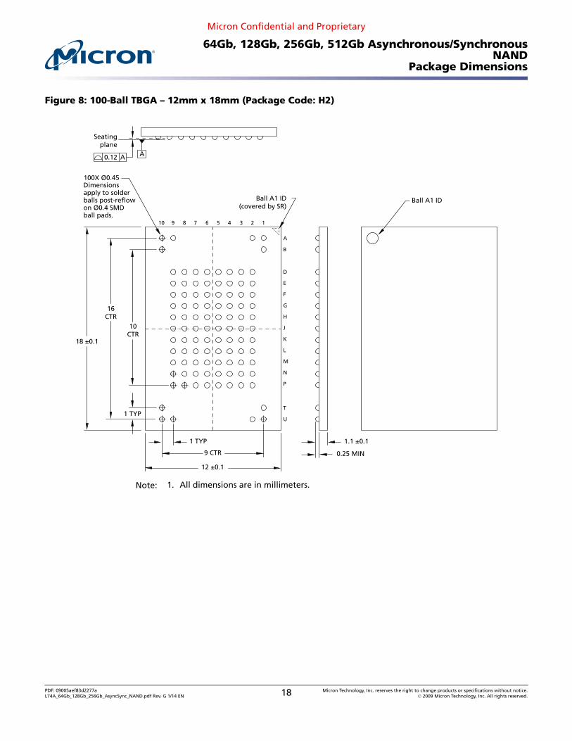
PDF: 09005aef83d2277aL74A_64Gb_128Gb_256Gb_AsyncSync_NAND.pdf Rev. G 1/14 EN 18 Micron Technology, Inc. reserves the right to change products or specifications without notice.
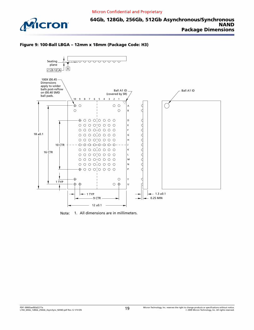
PDF: 09005aef83d2277aL74A_64Gb_128Gb_256Gb_AsyncSync_NAND.pdf Rev. G 1/14 EN 19 Micron Technology, Inc. reserves the right to change products or specifications without notice.
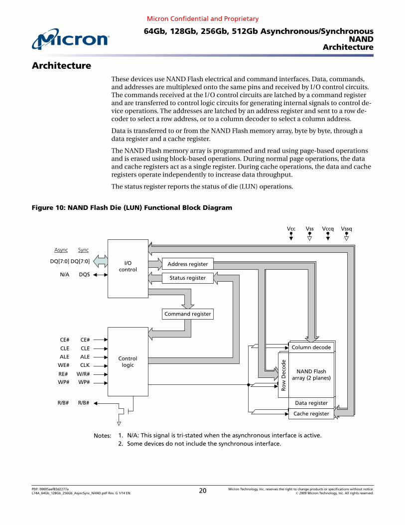
ArchitectureThese devices use NAND Flash electrical and command interfaces. Data, commands,and addresses are multiplexed onto the same pins and received by I/O control circuits.The commands received at the I/O control circuits are latched by a command registerand are transferred to control logic circuits for generating internal signals to control de-vice operations. The addresses are latched by an address register and sent to a row de-coder to select a row address, or to a column decoder to select a column address.
Data is transferred to or from the NAND Flash memory array, byte by byte, through adata register and a cache register.
The NAND Flash memory array is programmed and read using page-based operationsand is erased using block-based operations. During normal page operations, the dataand cache registers act as a single register. During cache operations, the data and cacheregisters operate independently to increase data throughput.
The status register reports the status of die (LUN) operations.
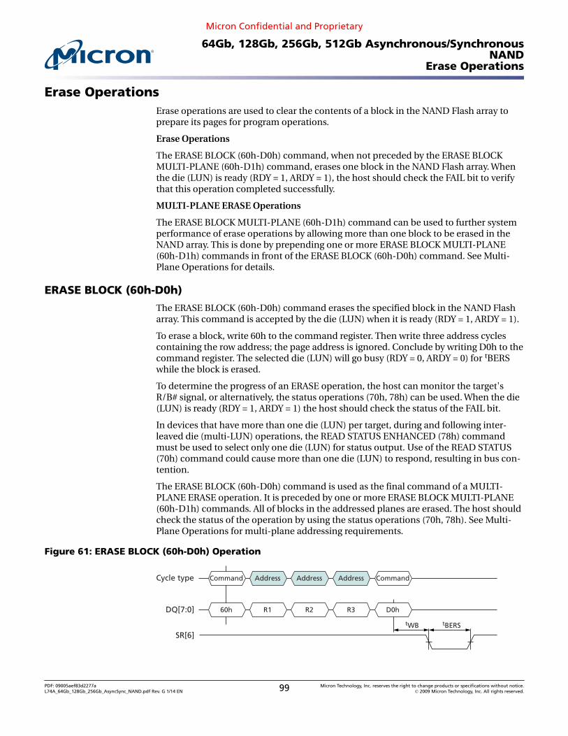
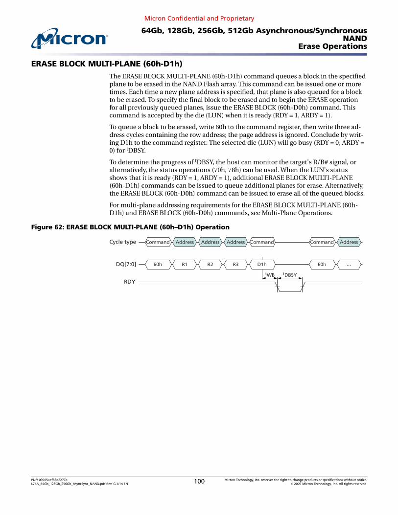
Figure 10: NAND Flash Die (LUN) Functional Block Diagram
Status register
Command register
Vccq Vssq
CE#
CLE
N/A
ALE
RE#
WP#
DQ[7:0]
Async
WE#
R/B#
CE#
CLE
DQS
ALE
W/R#
WP#
DQ[7:0]
Sync
CLK
R/B#
Vcc Vss
Controllogic
Data Register
Cache Register
Ro
w D
eco
de
Column Decode
NAND FlashArray
Data register
Cache register
Ro
w D
eco
de
Column decode
NAND Flash array (2 planes)
Address registerI/Ocontrol
Notes: 1. N/A: This signal is tri-stated when the asynchronous interface is active.2. Some devices do not include the synchronous interface.
PDF: 09005aef83d2277aL74A_64Gb_128Gb_256Gb_AsyncSync_NAND.pdf Rev. G 1/14 EN 20 Micron Technology, Inc. reserves the right to change products or specifications without notice.
PDF: 09005aef83d2277aL74A_64Gb_128Gb_256Gb_AsyncSync_NAND.pdf Rev. G 1/14 EN 21 Micron Technology, Inc. reserves the right to change products or specifications without notice.
PDF: 09005aef83d2277aL74A_64Gb_128Gb_256Gb_AsyncSync_NAND.pdf Rev. G 1/14 EN 22 Micron Technology, Inc. reserves the right to change products or specifications without notice.
PDF: 09005aef83d2277aL74A_64Gb_128Gb_256Gb_AsyncSync_NAND.pdf Rev. G 1/14 EN 23 Micron Technology, Inc. reserves the right to change products or specifications without notice.
PDF: 09005aef83d2277aL74A_64Gb_128Gb_256Gb_AsyncSync_NAND.pdf Rev. G 1/14 EN 24 Micron Technology, Inc. reserves the right to change products or specifications without notice.
PDF: 09005aef83d2277aL74A_64Gb_128Gb_256Gb_AsyncSync_NAND.pdf Rev. G 1/14 EN 25 Micron Technology, Inc. reserves the right to change products or specifications without notice.
PDF: 09005aef83d2277aL74A_64Gb_128Gb_256Gb_AsyncSync_NAND.pdf Rev. G 1/14 EN 26 Micron Technology, Inc. reserves the right to change products or specifications without notice.
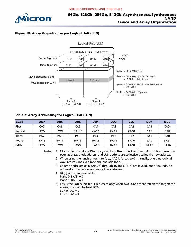
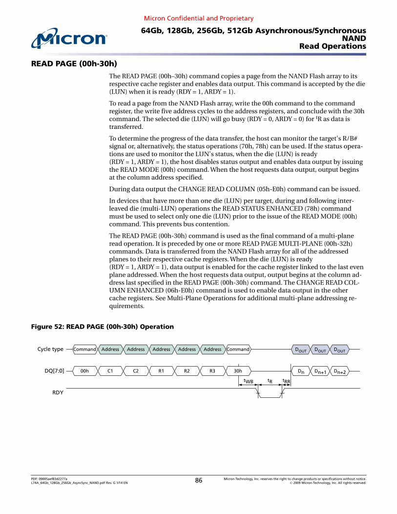
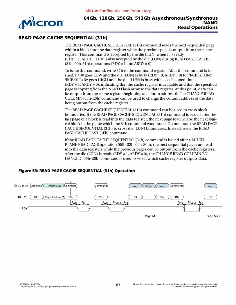
Notes: 1. CAx = column address, PAx = page address, BAx = block address, LAx = LUN address; thepage address, block address, and LUN address are collectively called the row address.
2. When using the synchronous interface, CA0 is forced to 0 internally; one data cycle al-ways returns one even byte and one odd byte.
3. Column addresses 8640 (21C0h) through 16,383 (3FFFh) are invalid, out of bounds, donot exist in the device, and cannot be addressed.
4. BA[8] is the plane-select bit:Plane 0: BA[8] = 0Plane 1: BA[8] = 1
5. LA0 is the LUN-select bit. It is present only when two LUNs are shared on the target; oth-erwise, it should be held LOW.LUN 0: LA0 = 0LUN 1: LA0 = 1
PDF: 09005aef83d2277aL74A_64Gb_128Gb_256Gb_AsyncSync_NAND.pdf Rev. G 1/14 EN 27 Micron Technology, Inc. reserves the right to change products or specifications without notice.
Bus Operation – Asynchronous InterfaceThe asynchronous interface is active when the NAND Flash device powers on. The I/Obus, DQ[7:0], is multiplexed sharing data I/O, addresses, and commands. The DQS sig-nal, if present, is tri-stated when the asynchronous interface is active.
Asynchronous interface bus modes are summarized below.
Table 3: Asynchronous Interface Mode Selection
Mode CE# CLE ALE WE# RE# DQS DQx WP# Notes
Standby H X X X X X X 0V/VCCQ2 2
Bus idle L X X H H X X X
Command input L H L H X input H
Address input L L H H X input H
Data input L L L H X input H
Data output L L L H X output X
Write protect X X X X X X X L
Notes: 1. DQS is tri-stated when the asynchronous interface is active.2. WP# should be biased to CMOS LOW or HIGH for standby.3. Mode selection settings for this table: H = Logic level HIGH; L = Logic level LOW; X = VIH
or VIL.
Asynchronous Enable/Standby
A chip enable (CE#) signal is used to enable or disable a target. When CE# is drivenLOW, all of the signals for that target are enabled. With CE# LOW, the target can acceptcommands, addresses, and data I/O. There may be more than one target in a NANDFlash package. Each target is controlled by its own chip enable; the first target (Target 0)is controlled by CE#; the second target (if present) is controlled by CE2#, etc.
A target is disabled when CE# is driven HIGH, even when the target is busy. When disa-bled, all of the target's signals are disabled except CE#, WP#, and R/B#. This functionali-ty is also known as CE# "Don't Care". While the target is disabled, other devices can uti-lize the disabled NAND signals that are shared with the NAND Flash.
A target enters low-power standby when it is disabled and is not busy. If the target isbusy when it is disabled, the target enters standby after all of the die (LUNs) completetheir operations. Standby helps reduce power consumption.
Asynchronous Bus Idle
A target's bus is idle when CE# is LOW, WE# is HIGH, and RE# is HIGH.
During bus idle, all of the signals are enabled except DQS, which is not used when theasynchronous interface is active. No commands, addresses, and data are latched intothe target; no data is output.
PDF: 09005aef83d2277aL74A_64Gb_128Gb_256Gb_AsyncSync_NAND.pdf Rev. G 1/14 EN 28 Micron Technology, Inc. reserves the right to change products or specifications without notice.
Pausing data input or data output is done by keeping WE# or RE# HIGH, respectively.
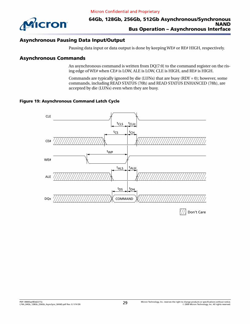
Asynchronous Commands
An asynchronous command is written from DQ[7:0] to the command register on the ris-ing edge of WE# when CE# is LOW, ALE is LOW, CLE is HIGH, and RE# is HIGH.
Commands are typically ignored by die (LUNs) that are busy (RDY = 0); however, somecommands, including READ STATUS (70h) and READ STATUS ENHANCED (78h), areaccepted by die (LUNs) even when they are busy.
PDF: 09005aef83d2277aL74A_64Gb_128Gb_256Gb_AsyncSync_NAND.pdf Rev. G 1/14 EN 29 Micron Technology, Inc. reserves the right to change products or specifications without notice.
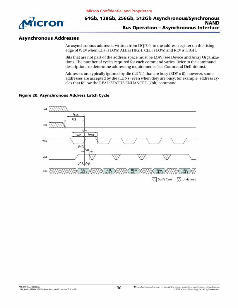
An asynchronous address is written from DQ[7:0] to the address register on the risingedge of WE# when CE# is LOW, ALE is HIGH, CLE is LOW, and RE# is HIGH.
Bits that are not part of the address space must be LOW (see Device and Array Organiza-tion). The number of cycles required for each command varies. Refer to the commanddescriptions to determine addressing requirements (see Command Definitions).
Addresses are typically ignored by die (LUNs) that are busy (RDY = 0); however, someaddresses are accepted by die (LUNs) even when they are busy; for example, address cy-cles that follow the READ STATUS ENHANCED (78h) command.
PDF: 09005aef83d2277aL74A_64Gb_128Gb_256Gb_AsyncSync_NAND.pdf Rev. G 1/14 EN 30 Micron Technology, Inc. reserves the right to change products or specifications without notice.
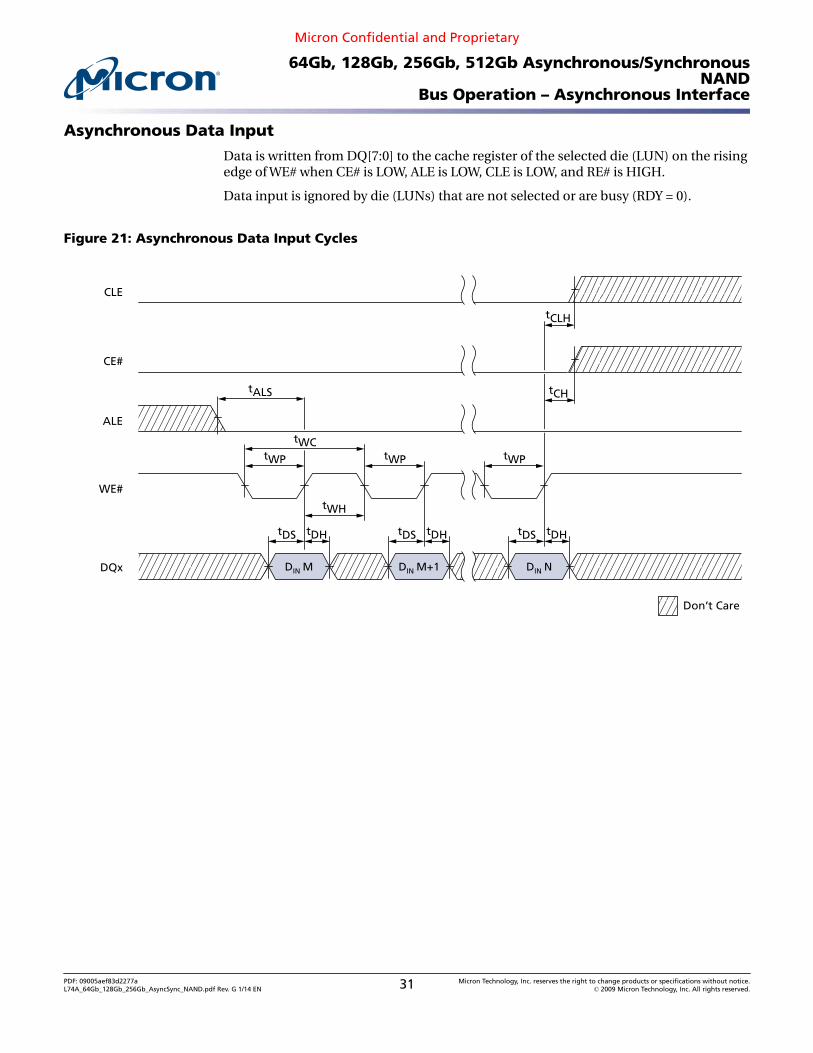
Data is written from DQ[7:0] to the cache register of the selected die (LUN) on the risingedge of WE# when CE# is LOW, ALE is LOW, CLE is LOW, and RE# is HIGH.
Data input is ignored by die (LUNs) that are not selected or are busy (RDY = 0).
PDF: 09005aef83d2277aL74A_64Gb_128Gb_256Gb_AsyncSync_NAND.pdf Rev. G 1/14 EN 31 Micron Technology, Inc. reserves the right to change products or specifications without notice.
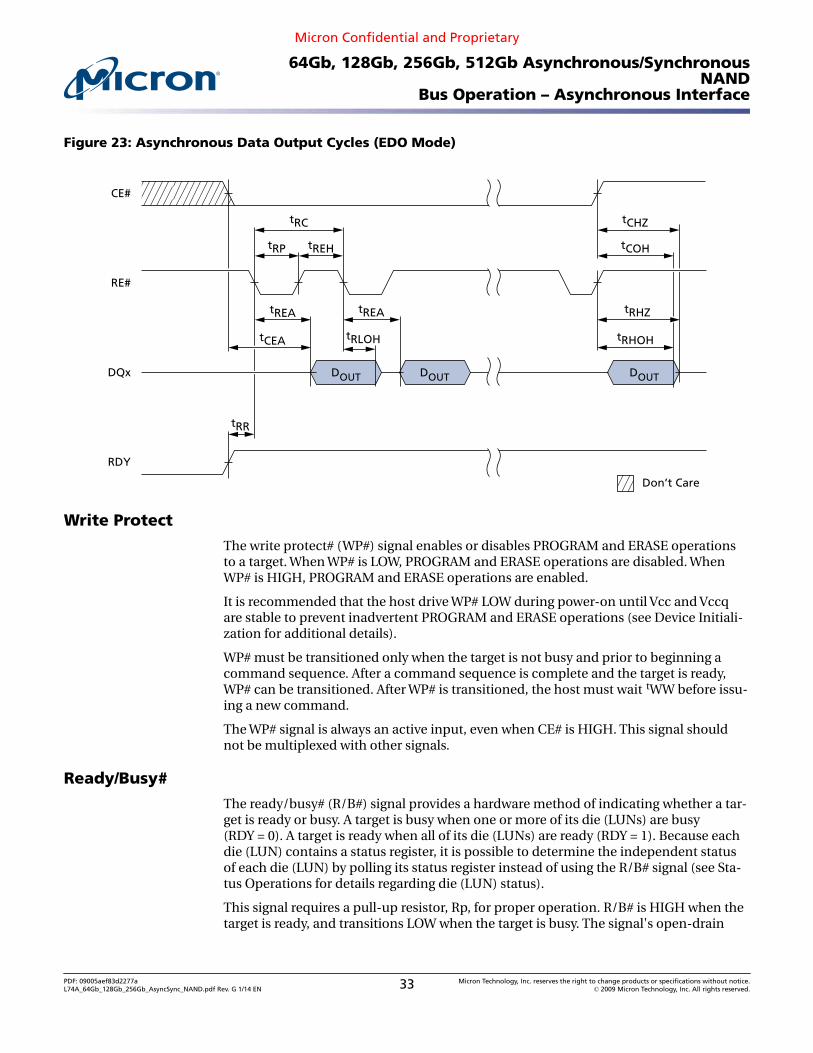
Data can be output from a die (LUN) if it is in a READY state. Data output is supportedfollowing a READ operation from the NAND Flash array. Data is output from the cacheregister of the selected die (LUN) to DQ[7:0] on the falling edge of RE# when CE# isLOW, ALE is LOW, CLE is LOW, and WE# is HIGH.
If the host controller is using a tRC of 30ns or greater, the host can latch the data on therising edge of RE# (see Figure 22 for proper timing). If the host controller is using a tRCof less than 30ns, the host can latch the data on the next falling edge of RE# (see Fig-ure 23 (page 33) for extended data output (EDO) timing).
Using the READ STATUS ENHANCED (78h) command prevents data contention follow-ing an interleaved die (multi-LUN) operation. After issuing the READ STATUS EN-HANCED (78h) command, to enable data output, issue the READ MODE (00h) com-mand.
Data output requests are typically ignored by a die (LUN) that is busy (RDY = 0); howev-er, it is possible to output data from the status register even when a die (LUN) is busy byfirst issuing the READ STATUS (70h) or READ STATUS ENHANCED (78h) command.
PDF: 09005aef83d2277aL74A_64Gb_128Gb_256Gb_AsyncSync_NAND.pdf Rev. G 1/14 EN 32 Micron Technology, Inc. reserves the right to change products or specifications without notice.
Figure 23: Asynchronous Data Output Cycles (EDO Mode)
DOUT DOUT DOUT
CE#
RE#
DQx
RDY
tRR
tCEA
tREA
tRP tREH
tRC
tRLOH
tREA
tRHOH
tRHZ
tCOH
tCHZ
Don’t Care
Write Protect
The write protect# (WP#) signal enables or disables PROGRAM and ERASE operationsto a target. When WP# is LOW, PROGRAM and ERASE operations are disabled. WhenWP# is HIGH, PROGRAM and ERASE operations are enabled.
It is recommended that the host drive WP# LOW during power-on until Vcc and Vccqare stable to prevent inadvertent PROGRAM and ERASE operations (see Device Initiali-zation for additional details).
WP# must be transitioned only when the target is not busy and prior to beginning acommand sequence. After a command sequence is complete and the target is ready,WP# can be transitioned. After WP# is transitioned, the host must wait tWW before issu-ing a new command.
The WP# signal is always an active input, even when CE# is HIGH. This signal shouldnot be multiplexed with other signals.
Ready/Busy#
The ready/busy# (R/B#) signal provides a hardware method of indicating whether a tar-get is ready or busy. A target is busy when one or more of its die (LUNs) are busy(RDY = 0). A target is ready when all of its die (LUNs) are ready (RDY = 1). Because eachdie (LUN) contains a status register, it is possible to determine the independent statusof each die (LUN) by polling its status register instead of using the R/B# signal (see Sta-tus Operations for details regarding die (LUN) status).
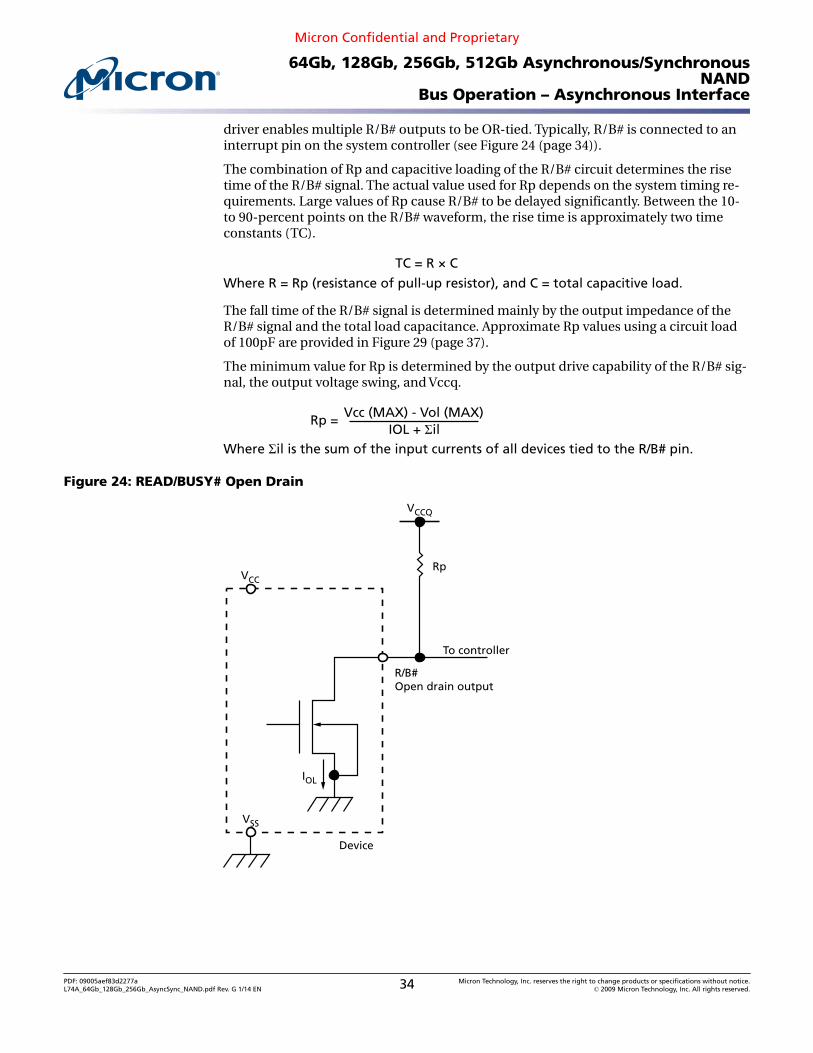
This signal requires a pull-up resistor, Rp, for proper operation. R/B# is HIGH when thetarget is ready, and transitions LOW when the target is busy. The signal's open-drain
PDF: 09005aef83d2277aL74A_64Gb_128Gb_256Gb_AsyncSync_NAND.pdf Rev. G 1/14 EN 33 Micron Technology, Inc. reserves the right to change products or specifications without notice.
driver enables multiple R/B# outputs to be OR-tied. Typically, R/B# is connected to aninterrupt pin on the system controller (see Figure 24 (page 34)).
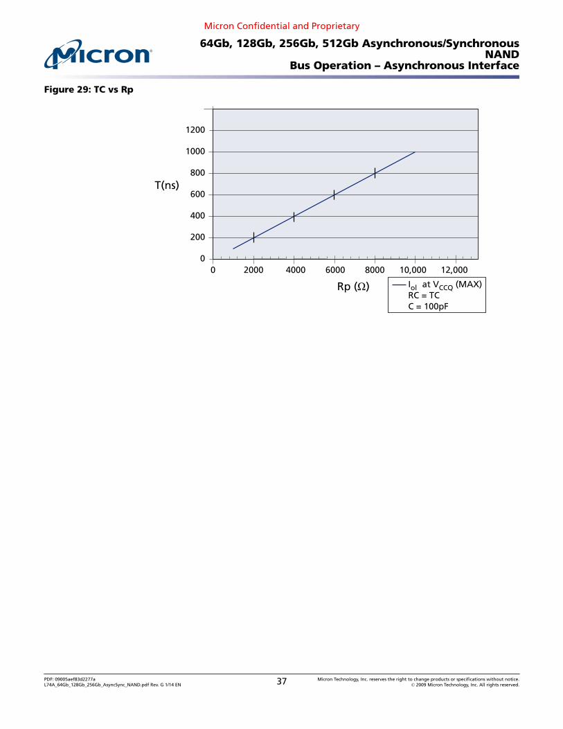
The combination of Rp and capacitive loading of the R/B# circuit determines the risetime of the R/B# signal. The actual value used for Rp depends on the system timing re-quirements. Large values of Rp cause R/B# to be delayed significantly. Between the 10-to 90-percent points on the R/B# waveform, the rise time is approximately two timeconstants (TC).
TC = R × C
Where R = Rp (resistance of pull-up resistor), and C = total capacitive load.
The fall time of the R/B# signal is determined mainly by the output impedance of theR/B# signal and the total load capacitance. Approximate Rp values using a circuit loadof 100pF are provided in Figure 29 (page 37).
The minimum value for Rp is determined by the output drive capability of the R/B# sig-nal, the output voltage swing, and Vccq.
Rp = Vcc (MAX) - Vol (MAX)IOL + Σil
Where Σil is the sum of the input currents of all devices tied to the R/B# pin.
PDF: 09005aef83d2277aL74A_64Gb_128Gb_256Gb_AsyncSync_NAND.pdf Rev. G 1/14 EN 34 Micron Technology, Inc. reserves the right to change products or specifications without notice.
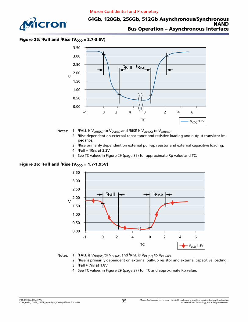
Notes: 1. tFALL is VOH(DC) to VOL(AC) and tRISE is VOL(DC) to VOH(AC).2. tRise dependent on external capacitance and resistive loading and output transistor im-
pedance.3. tRise primarily dependent on external pull-up resistor and external capacitive loading.4. tFall = 10ns at 3.3V5. See TC values in Figure 29 (page 37) for approximate Rp value and TC.
Figure 26: tFall and tRise (VCCQ = 1.7-1.95V)
3.50
3.00
2.50
2.00
1.50
1.00
0.50
0.00
-1 0 2 4 0 2 4 6
tFall tRise
VCCQ 1.8VTC
V
Notes: 1. tFALL is VOH(DC) to VOL(AC) and tRISE is VOL(DC) to VOH(AC).2. tRise is primarily dependent on external pull-up resistor and external capacitive loading.3. tFall ≈ 7ns at 1.8V.4. See TC values in Figure 29 (page 37) for TC and approximate Rp value.
PDF: 09005aef83d2277aL74A_64Gb_128Gb_256Gb_AsyncSync_NAND.pdf Rev. G 1/14 EN 35 Micron Technology, Inc. reserves the right to change products or specifications without notice.
PDF: 09005aef83d2277aL74A_64Gb_128Gb_256Gb_AsyncSync_NAND.pdf Rev. G 1/14 EN 36 Micron Technology, Inc. reserves the right to change products or specifications without notice.
PDF: 09005aef83d2277aL74A_64Gb_128Gb_256Gb_AsyncSync_NAND.pdf Rev. G 1/14 EN 37 Micron Technology, Inc. reserves the right to change products or specifications without notice.
Bus Operation – Synchronous InterfaceThese NAND Flash devices have two interfaces—a synchronous interface for fast dataI/O transfer and an asynchronous interface that is backward compatible with existingNAND Flash devices.
The NAND Flash command protocol for both the asynchronous and synchronous inter-faces is identical. However, there are some differences between the asynchronous andsynchronous interfaces when issuing command, address, and data I/O cycles using theNAND Flash signals.
When the synchronous interface is activated on a target (see Activating Interfaces), thetarget is capable of high-speed DDR data transfers. Existing signals are redefined forhigh-speed DDR I/O. The WE# signal becomes CLK. DQS is enabled. The RE# signal be-comes W/R#. CLK provides a clock reference to the NAND Flash device.
DQS is a bidirectional data strobe. During data output, DQS is driven by the NANDFlash device. During data input, DQS is controlled by the host controller while inputtingdata on DQ[7:0].
The direction of DQS and DQ[7:0] is controlled by the W/R# signal. When the W/R# sig-nal is latched HIGH, the controller is driving the DQ bus and DQS. When the W/R# islatched LOW, the NAND Flash is driving the DQ bus and DQS.
The synchronous interface bus modes are summarized below.
Table 4: Synchronous Interface Mode Selection
Mode CE# CLE ALE CLK W/R# DQS DQ[7:0] WP# Notes
Standby H X X X X X X 0V/VCCQ 1, 2
Bus idle L L L H X X X
Bus driv-ing
L L L L output output X
Commandinput
L H L H X input H 3
Addressinput
L L H H X input H 3
Data in-put
L H H H input H 4
Data out-put
L H H L See Note 5 output X 5
Write pro-tect
X X X X X X X L
Undefined L L H L output output X
Undefined L H L L output output X
Notes: 1. CLK can be stopped when the target is disabled, even when R/B# is LOW.2. WP# should be biased to CMOS LOW or HIGH for standby.3. Commands and addresses are latched on the rising edge of CLK.
PDF: 09005aef83d2277aL74A_64Gb_128Gb_256Gb_AsyncSync_NAND.pdf Rev. G 1/14 EN 38 Micron Technology, Inc. reserves the right to change products or specifications without notice.
4. During data input to the device, DQS is the “clock” that latches the data in the cacheregister.
5. During data output from the NAND Flash device, DQS is an output generated from CLKafter tDQSCK delay.
6. Mode selection settings for this table: H = Logic level HIGH; L = Logic level LOW; X = VIHor VIL.
Synchronous Enable/Standby
In addition to the description found in Asynchronous Enable/Standby (page 28), thefollowing requirements also apply when the synchronous interface is active.
Before enabling a target, CLK must be running and ALE and CLE must be LOW. WhenCE# is driven LOW, all of the signals for the selected target are enabled. The target is notenabled until tCS completes; the target's bus is then idle.
Prior to disabling a target, the target's bus must be idle. A target is disabled when CE# isdriven HIGH, even when it is busy. All of the target's signals are disabled except CE#,WP#, and R/B#. After the target is disabled, CLK can be stopped.
A target enters low-power standby when it is disabled and is not busy. If the target isbusy when it is disabled, the target enters standby after all of the die (LUNs) completetheir operations.
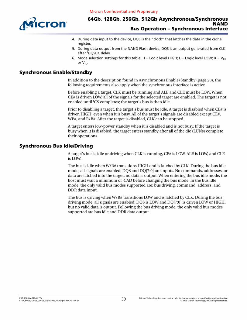
Synchronous Bus Idle/Driving
A target's bus is idle or driving when CLK is running, CE# is LOW, ALE is LOW, and CLEis LOW.
The bus is idle when W/R# transitions HIGH and is latched by CLK. During the bus idlemode, all signals are enabled; DQS and DQ[7:0] are inputs. No commands, addresses, ordata are latched into the target; no data is output. When entering the bus idle mode, thehost must wait a minimum of tCAD before changing the bus mode. In the bus idlemode, the only valid bus modes supported are: bus driving, command, address, andDDR data input.
The bus is driving when W/R# transitions LOW and is latched by CLK. During the busdriving mode, all signals are enabled; DQS is LOW and DQ[7:0] is driven LOW or HIGH,but no valid data is output. Following the bus driving mode, the only valid bus modessupported are bus idle and DDR data output.
PDF: 09005aef83d2277aL74A_64Gb_128Gb_256Gb_AsyncSync_NAND.pdf Rev. G 1/14 EN 39 Micron Technology, Inc. reserves the right to change products or specifications without notice.
Note: 1. Only the selected die (LUN) drives DQS and DQ[7:0]. During an interleaved die (multi-LUN) operation, the host must use the READ STATUS ENHANCED (78h) to prevent dataoutput contention.
Synchronous Pausing Data Input/Output
Pausing data input or data output is done by setting ALE and CLE to LOW. The host maycontinue data transfer by setting ALE and CLE to HIGH after the applicable tCAD timehas passed.
Synchronous Commands
A command is written from DQ[7:0] to the command register on the rising edge of CLKwhen CE# is LOW, ALE is LOW, CLE is HIGH, and W/R# is HIGH.
After a command is latched—and prior to issuing the next command, address, ordata I/O—the bus must go to bus idle mode on the next rising edge of CLK, exceptwhen the clock period, tCK, is greater than tCAD.
Commands are typically ignored by die (LUNs) that are busy (RDY = 0); however, somecommands, such as READ STATUS (70h) and READ STATUS ENHANCED (78h), are ac-cepted by die (LUNs), even when they are busy.
PDF: 09005aef83d2277aL74A_64Gb_128Gb_256Gb_AsyncSync_NAND.pdf Rev. G 1/14 EN 40 Micron Technology, Inc. reserves the right to change products or specifications without notice.
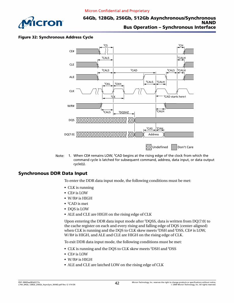
Note: 1. When CE# remains LOW, tCAD begins at the rising edge of the clock from which thecommand cycle is latched for subsequent command, address, data input, or data outputcycle(s).
Synchronous Addresses
A synchronous address is written from DQ[7:0] to the address register on the rising edgeof CLK when CE# is LOW, ALE is HIGH, CLE is LOW, and W/R# is HIGH.
After an address is latched—and prior to issuing the next command, address, or dataI/O—the bus must go to bus idle mode on the next rising edge of CLK, except when theclock period, tCK, is greater than tCAD.
Bits not part of the address space must be LOW (see Device and Array Organization).The number of address cycles required for each command varies. Refer to the com-mand descriptions to determine addressing requirements.
Addresses are typically ignored by die (LUNs) that are busy (RDY = 0); however, someaddresses such as address cycles that follow the READ STATUS ENHANCED (78h) com-mand, are accepted by die (LUNs), even when they are busy.
PDF: 09005aef83d2277aL74A_64Gb_128Gb_256Gb_AsyncSync_NAND.pdf Rev. G 1/14 EN 41 Micron Technology, Inc. reserves the right to change products or specifications without notice.
Note: 1. When CE# remains LOW, tCAD begins at the rising edge of the clock from which thecommand cycle is latched for subsequent command, address, data input, or data outputcycle(s).
Synchronous DDR Data Input
To enter the DDR data input mode, the following conditions must be met:
• CLK is running• CE# is LOW• W/R# is HIGH• tCAD is met• DQS is LOW• ALE and CLE are HIGH on the rising edge of CLK
Upon entering the DDR data input mode after tDQSS, data is written from DQ[7:0] tothe cache register on each and every rising and falling edge of DQS (center-aligned)when CLK is running and the DQS to CLK skew meets tDSH and tDSS, CE# is LOW,W/R# is HIGH, and ALE and CLE are HIGH on the rising edge of CLK.
To exit DDR data input mode, the following conditions must be met:
• CLK is running and the DQS to CLK skew meets tDSH and tDSS• CE# is LOW• W/R# is HIGH• ALE and CLE are latched LOW on the rising edge of CLK
PDF: 09005aef83d2277aL74A_64Gb_128Gb_256Gb_AsyncSync_NAND.pdf Rev. G 1/14 EN 42 Micron Technology, Inc. reserves the right to change products or specifications without notice.
• The final two data bytes of the data input sequence are written to DQ[7:0] to the cacheregister on the rising and falling edges of DQS after the last cycle in the data input se-quence in which ALE and CLE are latched HIGH.
• DQS is held LOW for tWPST (after the final falling edge of DQS)
Following tWPST, the bus enters bus idle mode and tCAD begins on the next rising edgeof CLK. After tCAD starts, the host can disable the target if desired.
Data input is ignored by die (LUNs) that are not selected or are busy.
Figure 33: Synchronous DDR Data Input Cycles
CLK
ALE
CLE
DQ[7:0]
DQS
tCKL tCALH
tDHtDS
tDQSS
tCALS
tCALHtCALS
Don’t Care
tCKH
tCALH
tCALS
tCALS
tCALHtCALStCALS
CE#
tCHtCS
tCAD
W/R#
tCK
tDQSLtWPRE tDQSLtDQSHtDQSH tDQSH tWPST
DN-1D2
tDSH tDSHtDSS tDSH tDSStDSH tDSS
tDHtDS
D3 DN-2 DND0 D1
tCADstartshere1
Notes: 1. When CE# remains LOW, tCAD begins at the first rising edge of the clock after tWPSTcompletes.
2. tDSH (MIN) generally occurs during tDQSS (MIN).3. tDSS (MIN) generally occurs during tDQSS (MAX).
Synchronous DDR Data Output
Data can be output from a die (LUN) if it is ready. Data output is supported following aREAD operation from the NAND Flash array.
To enter the DDR data output mode, the following conditions must be met:
• CLK is running• CE# is LOW• The host has released the DQ[7:0] bus and DQS• W/R# is latched LOW on the rising edge of CLK to enable the selected die (LUN) to
take ownership of the DQ[7:0] bus and DQS within tWRCK• tCAD is met• ALE and CLE are HIGH on the rising edge of CLK
PDF: 09005aef83d2277aL74A_64Gb_128Gb_256Gb_AsyncSync_NAND.pdf Rev. G 1/14 EN 43 Micron Technology, Inc. reserves the right to change products or specifications without notice.
Upon entering the DDR data output mode, DQS will toggle HIGH and LOW with a delayof tDQSCK from the respective rising and falling edges of CLK. DQ[7:0] will output dataedge-aligned to the rising and falling edges of DQS, with the first transition delayed byno more than tAC.
DDR data output mode continues as long as CLK is running, CE# is LOW, W/R# is LOW,and ALE and CLE are HIGH on the rising edge of CLK.
To exit DDR data output mode, the following conditions must be met:
• CLK is running• CE# is LOW• W/R# is LOW• ALE and CLE are latched LOW on the rising edge of CLK
The final two data bytes are output on DQ[7:0] on the final rising and falling edges ofDQS. The final rising and falling edges of DQS occur tDQSCK after the last cycle in thedata output sequence in which ALE and CLE are latched HIGH. After tCKWR, the busenters bus idle mode and tCAD begins on the next rising edge of CLK. Once tCAD startsthe host can disable the target if desired.
Data output requests are typically ignored by a die (LUN) that is busy (RDY = 0); howev-er, it is possible to output data from the status register even when a die (LUN) is busy byissuing the READ STATUS (70h) or READ STATUS ENHANCED (78h) command.
PDF: 09005aef83d2277aL74A_64Gb_128Gb_256Gb_AsyncSync_NAND.pdf Rev. G 1/14 EN 44 Micron Technology, Inc. reserves the right to change products or specifications without notice.
Notes: 1. When CE# remains LOW, tCAD begins at the rising edge of the clock after tCKWR forsubsequent command or data output cycle(s).
2. See Figure 31 (page 41) for details of W/R# behavior.3. tAC is the DQ output window relative to CLK and is the long-term component of DQ
skew.4. For W/R# transitioning HIGH, DQ[7:0] and DQS go to tri-state.5. For W/R# transitioning LOW, DQ[7:0] drives current state and DQS goes LOW.6. After final data output, DQ[7:0] is driven until W/R# goes HIGH, but is not valid.
PDF: 09005aef83d2277aL74A_64Gb_128Gb_256Gb_AsyncSync_NAND.pdf Rev. G 1/14 EN 45 Micron Technology, Inc. reserves the right to change products or specifications without notice.
Device InitializationSome NAND Flash devices do not support VCCQ. For these devices all references to V CCQare replaced with VCC.
Micron NAND Flash devices are designed to prevent data corruption during powertransitions. VCC is internally monitored. (The WP# signal supports additional hardwareprotection during power transitions.) When ramping V CC and VCCQ, use the followingprocedure to initialize the device:
1. Ramp VCC.2. Ramp VCCQ. VCCQ must not exceed VCC.3. The host must wait for R/B# to be valid and HIGH before issuing RESET (FFh) to
any target (see Figure 35). The R/B# signal becomes valid when 50µs has elapsedsince the beginning the VCC ramp, and 10µs has elapsed since VCCQ reaches VCCQ(MIN) and VCC reaches VCC (MIN).
4. If not monitoring R/B#, the host must wait at least 100µs after VCCQ reaches VCCQ(MIN) and VCC reaches VCC (MIN). If monitoringR/B#, the host must wait until R/B# is HIGH.
5. The asynchronous interface is active by default for each target. Each LUN drawsless than an average of IST measured over intervals of 1ms until the RESET (FFh)command is issued.
6. The RESET (FFh) command must be the first command issued to all targets (CE#s)after the NAND Flash device is powered on. Each target will be busy for tPOR aftera RESET command is issued. The RESET busy time can be monitored by pollingR/B# or issuing the READ STATUS (70h) command to poll the status register.
7. The device is now initialized and ready for normal operation.
At power-down, VCCQ must go LOW, either before, or simultaneously with, VCC goingLOW.
Figure 35: R/B# Power-On Behavior
Reset (FFh)is issued
50µs (MIN)
100µs (MAX)
Invalid
10µs(MAX)
> 0µs
Vcc rampstarts
Vccq
Vcc
R/B#
Vccq = Vccq (MIN)
Vcc = Vcc (MIN)
Note: 1. Disregard VCCQ for devices that use only VCC.
To initialize a discovered target, the following steps shall be taken. The initializationprocess should be followed for each connected CE# signal, including performing theREAD PARAMETER PAGE (ECh) command for each target. Each chip enable corre-
PDF: 09005aef83d2277aL74A_64Gb_128Gb_256Gb_AsyncSync_NAND.pdf Rev. G 1/14 EN 46 Micron Technology, Inc. reserves the right to change products or specifications without notice.
sponds to a unique target with its own independent properties that the host shall ob-serve and subsequently use.
The host should issue the READ PARAMETET PAGE (ECh) command. This commandreturns information that includes the capabilities, features, and operating parametersof the device. When the information is read from the device, the host shall check theCRC to ensure that the data was received correctly and without error prior to taking ac-tion on that data.
If the CRC of the first parameter page read is not valid, the host should read redundantparameter page copies. The host can determine whether a redundant parameter page ispresent or not by checking if the first four bytes contain at least two bytes of the param-eter page signature. If the parameter page signature is present, then the host shouldread the entirety of that redundant parameter page. The host should then check theCRC of that redundant parameter page. If the CRC is correct, the host may take actionbased on the contents of that redundant parameter page. If the CRC is incorrect, thenthe host should attempt to read the next redundant parameter page by the same proce-dure.
The host should continue reading redundant parameter pages until the host is able toaccurately reconstruct the parameter page contents. The host may use bit-wise majorityor other ECC techniques to recover the contents of the parameter page from the param-eter page copies present. When the host determines that a parameter page signature isnot present, then all parameter pages have been read.
After successfully retrieving the parameter page, the host has all information necessaryto successfully communicate with that target. If the host has not previously mapped de-fective block information for this target, the host should next map out all defectiveblocks in the target. The host may then proceed to utilize the target, including erase andprogram operations.
PDF: 09005aef83d2277aL74A_64Gb_128Gb_256Gb_AsyncSync_NAND.pdf Rev. G 1/14 EN 47 Micron Technology, Inc. reserves the right to change products or specifications without notice.
Activating InterfacesAfter performing the steps under Device Initialization (page 46), the asynchronous in-terface is active for all targets on the device.
Each target's interface is independent of other targets, so the host is responsible forchanging the interface for each target.
If the host and NAND Flash device, through error, are no longer using the same inter-face, then steps under Activating the Asynchronous Interface are performed to re-synchronize the interfaces.
Activating the Asynchronous Interface
To activate the asynchronous NAND interface, once the synchronous interface is active,the following steps are repeated for each target:
1. The host pulls CE# HIGH, disables its input to CLK, and enables its asynchronousinterface.
2. The host pulls CE# LOW and issues the RESET (FFh) command, using an asyn-chronous command cycle.
3. R/B# goes LOW for tRST.4. After tITC, and during tRST, the device enters the asynchronous NAND interface.
READ STATUS (70h) and READ STATUS ENHANCED (78h) are the only commandsthat can be issued.
5. After tRST, R/B# goes HIGH. Timing mode feature address (01h), subfeature pa-rameter P1 is set to 00h, indicating that the asynchronous NAND interface is activeand that the device is set to timing mode 0.
For further details, see Reset Operations.
Activating the Synchronous Interface
To activate the synchronous NAND Flash interface, the following steps are repeated foreach target:
1. Issue the SET FEATURES (EFh) command.2. Write address 01h, which selects the timing mode.3. Write P1 with 1Xh, where "X" is the timing mode used in the synchronous inter-
face (see Configuration Operations).4. Write P2–P4 as 00h-00h-00h.5. R/B# goes LOW for tITC. The host should pull CE# HIGH. During tITC, the host
should not issue any type of command, including status commands, to the NANDFlash device.
6. After tITC, R/B# goes HIGH and the synchronous interface is enabled. Before pull-ing CE# LOW, the host should enable the clock.
PDF: 09005aef83d2277aL74A_64Gb_128Gb_256Gb_AsyncSync_NAND.pdf Rev. G 1/14 EN 48 Micron Technology, Inc. reserves the right to change products or specifications without notice.
PDF: 09005aef83d2277aL74A_64Gb_128Gb_256Gb_AsyncSync_NAND.pdf Rev. G 1/14 EN 49 Micron Technology, Inc. reserves the right to change products or specifications without notice.
PDF: 09005aef83d2277aL74A_64Gb_128Gb_256Gb_AsyncSync_NAND.pdf Rev. G 1/14 EN 50 Micron Technology, Inc. reserves the right to change products or specifications without notice.
Notes: 1. Busy means RDY = 0.2. These commands can be used for interleaved die (multi-LUN) operations (see Interleaved
Die (Multi-LUN) Operations (page 110)).3. The READ ID (90h) and GET FEATURES (EEh) output identical data on rising and falling
DQS edges.4. The SET FEATURES (EFh) command requires data transition prior to the rising edge of
CLK, with identical data for the rising and falling edges.5. Command cycle #2 of 11h is conditional. See CHANGE ROW ADDRESS (85h) for more de-
tails.6. This command can be preceded by up to one READ PAGE MULTI-PLANE (00h-32h) com-
mand to accommodate a maximum simultaneous two-plane array operation.7. Issuing a READ PAGE CACHE-series (31h, 00h-31h, 00h-32h, 3Fh) command when the ar-
ray is busy (RDY = 1, ARDY = 0) is supported if the previous command was a READ PAGE(00h-30h) or READ PAGE CACHE-series command; otherwise, it is prohibited.
8. Issuing a PROGRAM PAGE CACHE (80h-15h) command when the array is busy (RDY = 1,ARDY = 0) is supported if the previous command was a PROGRAM PAGE CACHE(80h-15h) command; otherwise, it is prohibited.
PDF: 09005aef83d2277aL74A_64Gb_128Gb_256Gb_AsyncSync_NAND.pdf Rev. G 1/14 EN 51 Micron Technology, Inc. reserves the right to change products or specifications without notice.
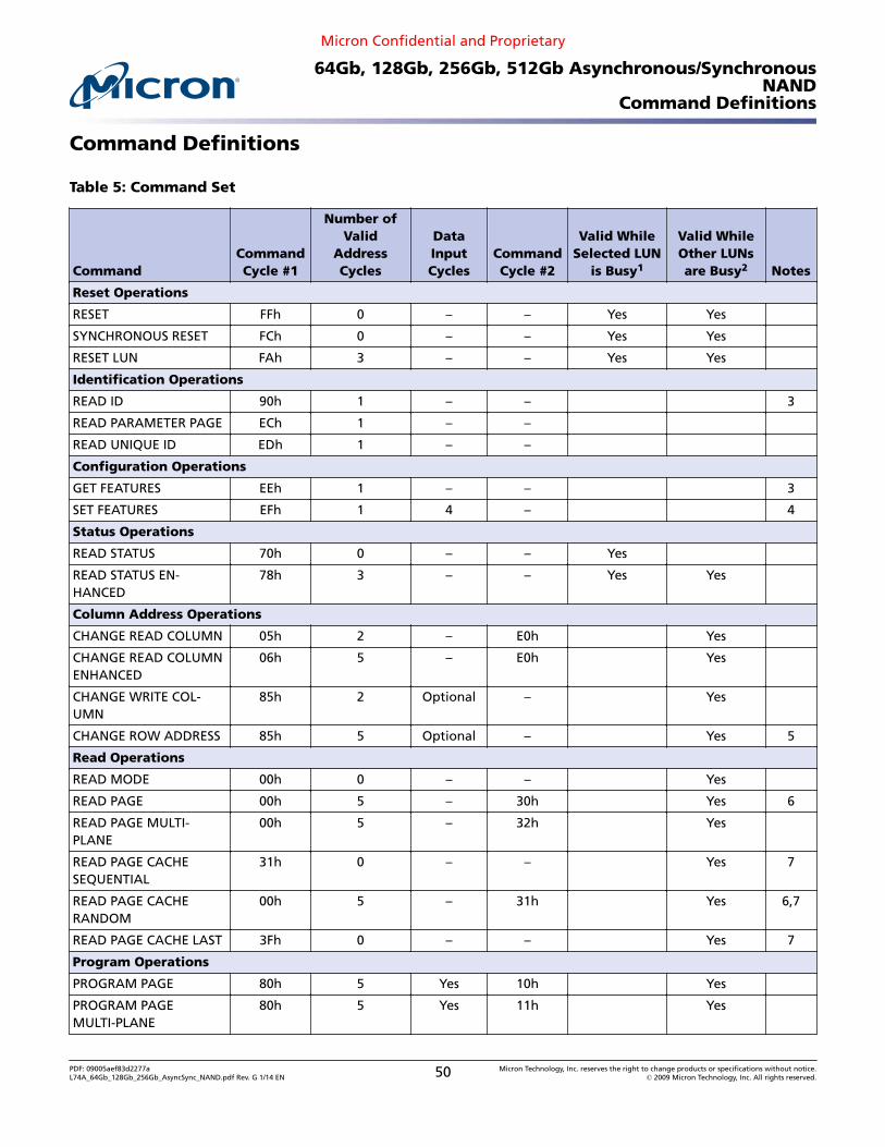
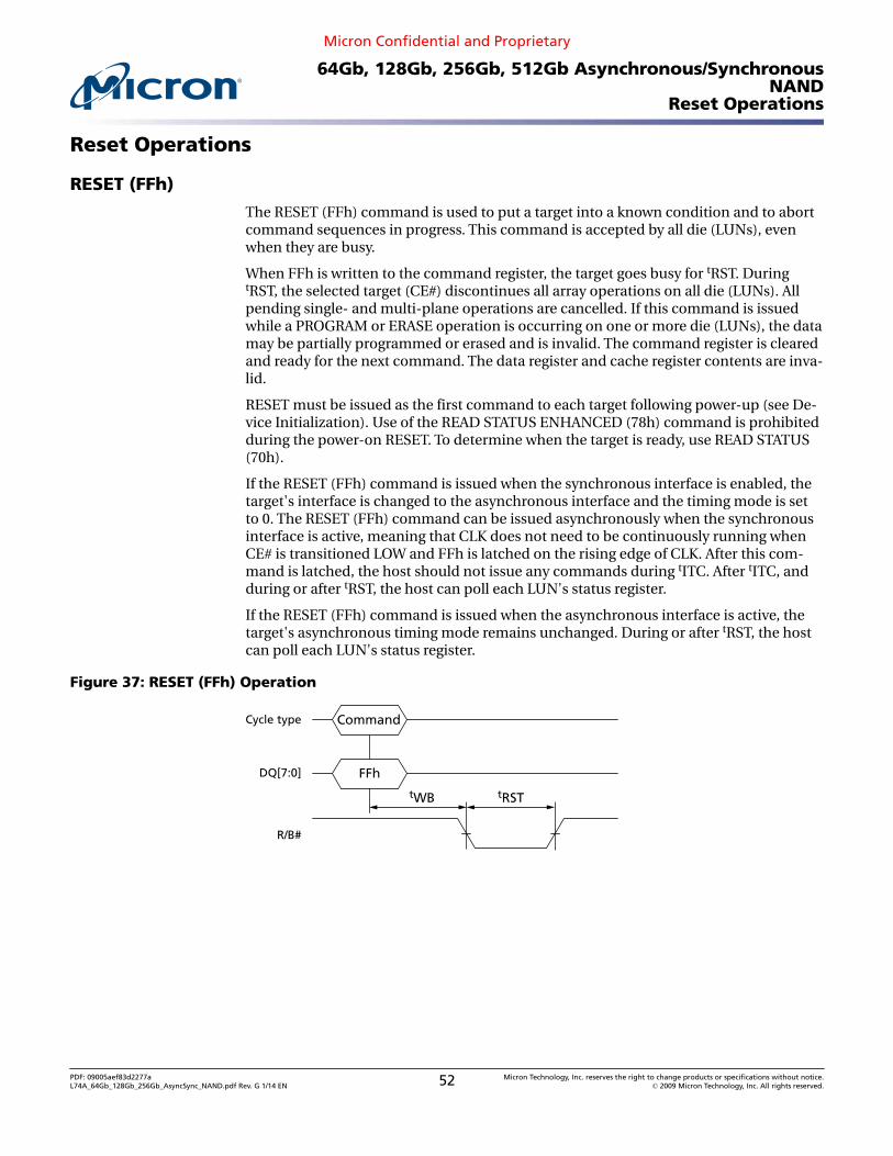
The RESET (FFh) command is used to put a target into a known condition and to abortcommand sequences in progress. This command is accepted by all die (LUNs), evenwhen they are busy.
When FFh is written to the command register, the target goes busy for tRST. DuringtRST, the selected target (CE#) discontinues all array operations on all die (LUNs). Allpending single- and multi-plane operations are cancelled. If this command is issuedwhile a PROGRAM or ERASE operation is occurring on one or more die (LUNs), the datamay be partially programmed or erased and is invalid. The command register is clearedand ready for the next command. The data register and cache register contents are inva-lid.
RESET must be issued as the first command to each target following power-up (see De-vice Initialization). Use of the READ STATUS ENHANCED (78h) command is prohibitedduring the power-on RESET. To determine when the target is ready, use READ STATUS(70h).
If the RESET (FFh) command is issued when the synchronous interface is enabled, thetarget's interface is changed to the asynchronous interface and the timing mode is setto 0. The RESET (FFh) command can be issued asynchronously when the synchronousinterface is active, meaning that CLK does not need to be continuously running whenCE# is transitioned LOW and FFh is latched on the rising edge of CLK. After this com-mand is latched, the host should not issue any commands during tITC. After tITC, andduring or after tRST, the host can poll each LUN's status register.
If the RESET (FFh) command is issued when the asynchronous interface is active, thetarget's asynchronous timing mode remains unchanged. During or after tRST, the hostcan poll each LUN's status register.
PDF: 09005aef83d2277aL74A_64Gb_128Gb_256Gb_AsyncSync_NAND.pdf Rev. G 1/14 EN 52 Micron Technology, Inc. reserves the right to change products or specifications without notice.
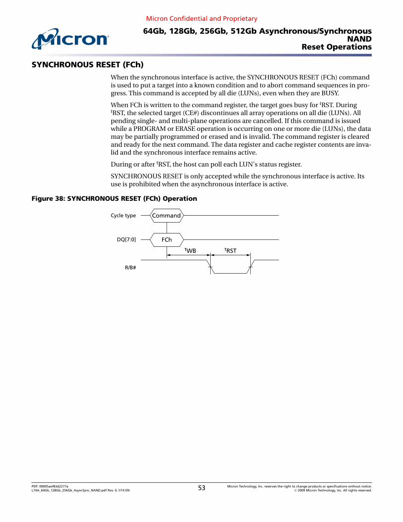
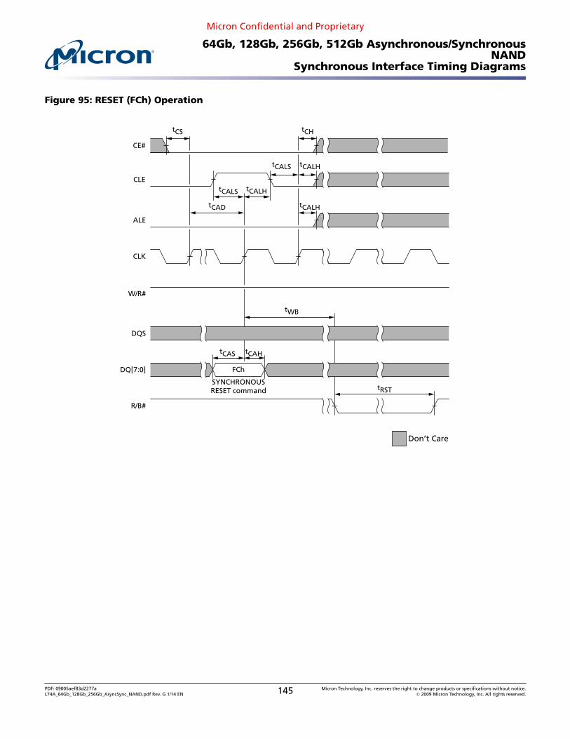
When the synchronous interface is active, the SYNCHRONOUS RESET (FCh) commandis used to put a target into a known condition and to abort command sequences in pro-gress. This command is accepted by all die (LUNs), even when they are BUSY.
When FCh is written to the command register, the target goes busy for tRST. DuringtRST, the selected target (CE#) discontinues all array operations on all die (LUNs). Allpending single- and multi-plane operations are cancelled. If this command is issuedwhile a PROGRAM or ERASE operation is occurring on one or more die (LUNs), the datamay be partially programmed or erased and is invalid. The command register is clearedand ready for the next command. The data register and cache register contents are inva-lid and the synchronous interface remains active.
During or after tRST, the host can poll each LUN's status register.
SYNCHRONOUS RESET is only accepted while the synchronous interface is active. Itsuse is prohibited when the asynchronous interface is active.
PDF: 09005aef83d2277aL74A_64Gb_128Gb_256Gb_AsyncSync_NAND.pdf Rev. G 1/14 EN 53 Micron Technology, Inc. reserves the right to change products or specifications without notice.
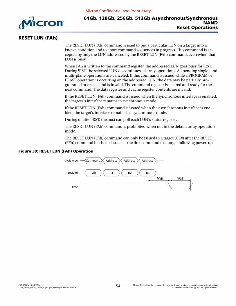
The RESET LUN (FAh) command is used to put a particular LUN on a target into aknown condition and to abort command sequences in progress. This command is ac-cepted by only the LUN addressed by the RESET LUN (FAh) command, even when thatLUN is busy.
When FAh is written to the command register, the addressed LUN goes busy for tRST.During tRST, the selected LUN discontinues all array operations. All pending single- andmulti-plane operations are canceled. If this command is issued while a PROGRAM orERASE operation is occurring on the addressed LUN, the data may be partially pro-grammed or erased and is invalid. The command register is cleared and ready for thenext command. The data register and cache register contents are invalid.
If the RESET LUN (FAh) command is issued when the synchronous interface is enabled,the targets's interface remains in synchronous mode.
If the RESET LUN (FAh) command is issued when the asynchronous interface is ena-bled, the target's interface remains in asynchronous mode.
During or after tRST, the host can poll each LUN's status register.
The RESET LUN (FAh) command is prohibited when not in the default array operationmode.
The RESET LUN (FAh) command can only be issued to a target (CE#) after the RESET(FFh) command has been issued as the first command to a target following power-up.
PDF: 09005aef83d2277aL74A_64Gb_128Gb_256Gb_AsyncSync_NAND.pdf Rev. G 1/14 EN 54 Micron Technology, Inc. reserves the right to change products or specifications without notice.
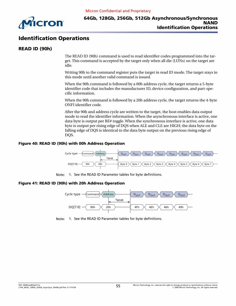
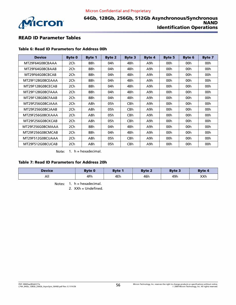
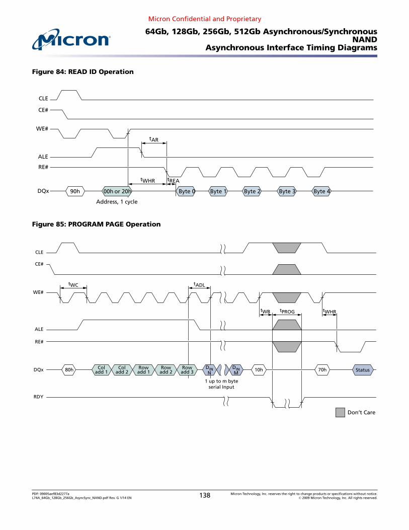
The READ ID (90h) command is used to read identifier codes programmed into the tar-get. This command is accepted by the target only when all die (LUNs) on the target areidle.
Writing 90h to the command register puts the target in read ID mode. The target stays inthis mode until another valid command is issued.
When the 90h command is followed by a 00h address cycle, the target returns a 5-byteidentifier code that includes the manufacturer ID, device configuration, and part-spe-cific information.
When the 90h command is followed by a 20h address cycle, the target returns the 4-byteONFI identifier code.
After the 90h and address cycle are written to the target, the host enables data outputmode to read the identifier information. When the asynchronous interface is active, onedata byte is output per RE# toggle. When the synchronous interface is active, one databyte is output per rising edge of DQS when ALE and CLE are HIGH; the data byte on thefalling edge of DQS is identical to the data byte output on the previous rising edge ofDQS.
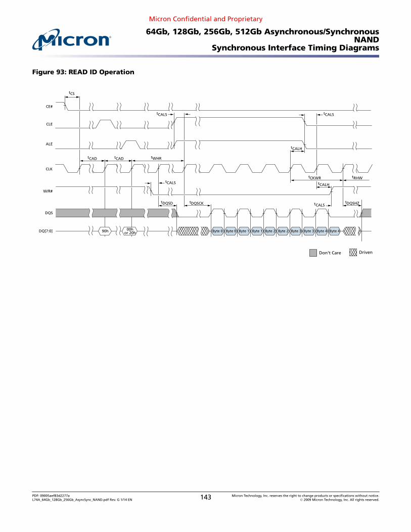
Figure 40: READ ID (90h) with 00h Address Operation
Cycle type
DQ[7:0]
tWHR
Command
90h 00h Byte 0 Byte 1 Byte 2 Byte 3
Address DOUT DOUT DOUT DOUT DOUT DOUT DOUT DOUT
Byte 4 Byte 5 Byte 6 Byte 7
Note: 1. See the READ ID Parameter tables for byte definitions.
Figure 41: READ ID (90h) with 20h Address Operation
Cycle type
DQ[7:0]
tWHR
Command
90h 20h 4Fh 4Eh 46h 49h
Address DOUT DOUT DOUT DOUT
Note: 1. See the READ ID Parameter tables for byte definitions.
PDF: 09005aef83d2277aL74A_64Gb_128Gb_256Gb_AsyncSync_NAND.pdf Rev. G 1/14 EN 55 Micron Technology, Inc. reserves the right to change products or specifications without notice.
PDF: 09005aef83d2277aL74A_64Gb_128Gb_256Gb_AsyncSync_NAND.pdf Rev. G 1/14 EN 56 Micron Technology, Inc. reserves the right to change products or specifications without notice.
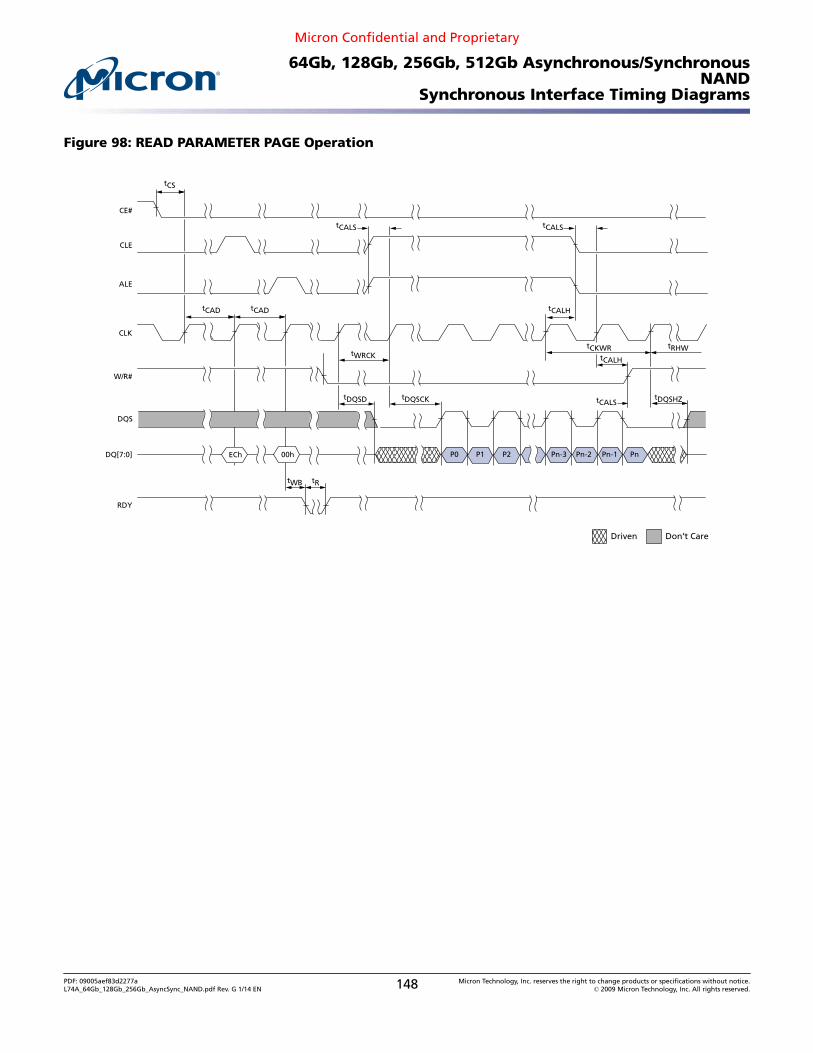
The READ PARAMETER PAGE (ECh) command is used to read the ONFI parameter pageprogrammed into the target. This command is accepted by the target only when all die(LUNs) on the target are idle.
Writing ECh to the command register puts the target in read parameter page mode. Thetarget stays in this mode until another valid command is issued.
When the ECh command is followed by an 00h address cycle, the target goes busy for tR.If the READ STATUS (70h) command is used to monitor for command completion, theREAD MODE (00h) command must be used to re-enable data output mode. Use of theREAD STATUS ENHANCED (78h) command is prohibited while the target is busy andduring data output.
After tR completes, the host enables data output mode to read the parameter page.When the asynchronous interface is active, one data byte is output per RE# toggle.When the synchronous interface is active, one data byte is output for each rising or fall-ing edge of DQS.
A minimum of three copies of the parameter page are stored in the device. Each param-eter page is 256 bytes. If desired, the CHANGE READ COLUMN (05h-E0h) commandcan be used to change the location of data output. Use of the CHANGE READ COLUMNENHANCED (06h-E0h) command is prohibited.
The READ PARAMETER PAGE (ECh) output data can be used by the host to configure itsinternal settings to properly use the NAND Flash device. Parameter page data is staticper part, however the value can be changed through the product cycle of NAND Flash.The host should interpret the data and configure itself accordingly.
PDF: 09005aef83d2277aL74A_64Gb_128Gb_256Gb_AsyncSync_NAND.pdf Rev. G 1/14 EN 57 Micron Technology, Inc. reserves the right to change products or specifications without notice.
PDF: 09005aef83d2277aL74A_64Gb_128Gb_256Gb_AsyncSync_NAND.pdf Rev. G 1/14 EN 58 Micron Technology, Inc. reserves the right to change products or specifications without notice.
PDF: 09005aef83d2277aL74A_64Gb_128Gb_256Gb_AsyncSync_NAND.pdf Rev. G 1/14 EN 59 Micron Technology, Inc. reserves the right to change products or specifications without notice.
PDF: 09005aef83d2277aL74A_64Gb_128Gb_256Gb_AsyncSync_NAND.pdf Rev. G 1/14 EN 60 Micron Technology, Inc. reserves the right to change products or specifications without notice.
PDF: 09005aef83d2277aL74A_64Gb_128Gb_256Gb_AsyncSync_NAND.pdf Rev. G 1/14 EN 61 Micron Technology, Inc. reserves the right to change products or specifications without notice.
PDF: 09005aef83d2277aL74A_64Gb_128Gb_256Gb_AsyncSync_NAND.pdf Rev. G 1/14 EN 62 Micron Technology, Inc. reserves the right to change products or specifications without notice.
143 Source synchronous featuresBit[7:3]: Reserved (0)Bit 2: 1 = devices support CLK stopped for data inputBit 1: 1 = typical capacitance values presentBit 0: 0 = use tCAD MIN value
PDF: 09005aef83d2277aL74A_64Gb_128Gb_256Gb_AsyncSync_NAND.pdf Rev. G 1/14 EN 63 Micron Technology, Inc. reserves the right to change products or specifications without notice.
PDF: 09005aef83d2277aL74A_64Gb_128Gb_256Gb_AsyncSync_NAND.pdf Rev. G 1/14 EN 64 Micron Technology, Inc. reserves the right to change products or specifications without notice.
PDF: 09005aef83d2277aL74A_64Gb_128Gb_256Gb_AsyncSync_NAND.pdf Rev. G 1/14 EN 65 Micron Technology, Inc. reserves the right to change products or specifications without notice.
PDF: 09005aef83d2277aL74A_64Gb_128Gb_256Gb_AsyncSync_NAND.pdf Rev. G 1/14 EN 66 Micron Technology, Inc. reserves the right to change products or specifications without notice.
PDF: 09005aef83d2277aL74A_64Gb_128Gb_256Gb_AsyncSync_NAND.pdf Rev. G 1/14 EN 67 Micron Technology, Inc. reserves the right to change products or specifications without notice.
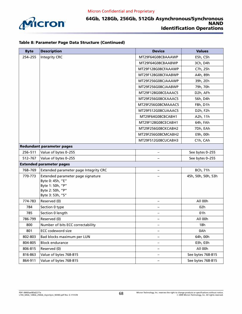
PDF: 09005aef83d2277aL74A_64Gb_128Gb_256Gb_AsyncSync_NAND.pdf Rev. G 1/14 EN 68 Micron Technology, Inc. reserves the right to change products or specifications without notice.
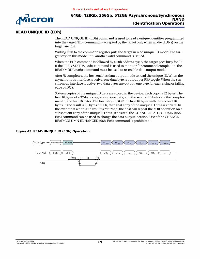
The READ UNIQUE ID (EDh) command is used to read a unique identifier programmedinto the target. This command is accepted by the target only when all die (LUNs) on thetarget are idle.
Writing EDh to the command register puts the target in read unique ID mode. The tar-get stays in this mode until another valid command is issued.
When the EDh command is followed by a 00h address cycle, the target goes busy for tR.If the READ STATUS (70h) command is used to monitor for command completion, theREAD MODE (00h) command must be used to re-enable data output mode.
After tR completes, the host enables data output mode to read the unique ID. When theasynchronous interface is active, one data byte is output per RE# toggle. When the syn-chronous interface is active, two data bytes are output, one byte for each rising or fallingedge of DQS.
Sixteen copies of the unique ID data are stored in the device. Each copy is 32 bytes. Thefirst 16 bytes of a 32-byte copy are unique data, and the second 16 bytes are the comple-ment of the first 16 bytes. The host should XOR the first 16 bytes with the second 16bytes. If the result is 16 bytes of FFh, then that copy of the unique ID data is correct. Inthe event that a non-FFh result is returned, the host can repeat the XOR operation on asubsequent copy of the unique ID data. If desired, the CHANGE READ COLUMN (05h-E0h) command can be used to change the data output location. Use of the CHANGEREAD COLUMN ENHANCED (06h-E0h) command is prohibited.
PDF: 09005aef83d2277aL74A_64Gb_128Gb_256Gb_AsyncSync_NAND.pdf Rev. G 1/14 EN 69 Micron Technology, Inc. reserves the right to change products or specifications without notice.
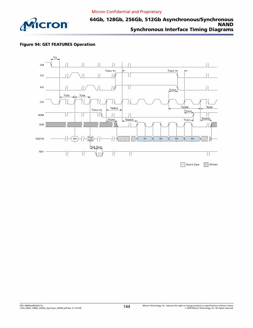
Configuration OperationsThe SET FEATURES (EFh) and GET FEATURES (EEh) commands are used to modify thetarget's default power-on behavior. These commands use a one-byte feature address todetermine which subfeature parameters will be read or modified. Each feature address(in the 00h to FFh range) is defined in Table 9. The SET FEATURES (EFh) commandwrites subfeature parameters (P1-P4) to the specified feature address. The GET FEA-TURES command reads the subfeature parameters (P1-P4) at the specified feature ad-dress.
Unless otherwise specifed, the values of the feature addresses do not change when RE-SET (FFh, FCh) is issued by the host.
Table 9: Feature Address Definitions
Feature Address Definition
00h Reserved
01h Timing mode
02h–0Fh Reserved
10h Programmable output drive strength
11h–7Fh Reserved
80h Programmable output drive strength
81h Programmable RB# pull-down strength
82h–8Fh Reserved
90h Array operation mode
91h–FFh Reserved
SET FEATURES (EFh)
The SET FEATURES (EFh) command writes the subfeature parameters (P1-P4) to thespecified feature address to enable or disable target-specific features. This command isaccepted by the target only when all die (LUNs) on the target are idle.
Writing EFh to the command register puts the target in the set features mode. The targetstays in this mode until another command is issued.
The EFh command is followed by a valid feature address as specified in Table 9. Thehost waits for tADL before the subfeature parameters are input. When the asynchronousinterface is active, one subfeature parameter is latched per rising edge of WE#. Whenthe synchronous interface is active, one subfeature parameter is latched per rising edgeof DQS. The data on the falling edge of DQS should be identical to the subfeature pa-rameter input on the previous rising edge of DQS. The device is not required to wait forthe repeated data byte before beginning internal actions.
After all four subfeature parameters are input, the target goes busy for tFEAT. The READSTATUS (70h) command can be used to monitor for command completion.
Feature address 01h (timing mode) operation is unique. If SET FEATURES is used tomodify the interface type, the target will be busy for tITC. See Activating Interfaces(page 48) for details.
PDF: 09005aef83d2277aL74A_64Gb_128Gb_256Gb_AsyncSync_NAND.pdf Rev. G 1/14 EN 70 Micron Technology, Inc. reserves the right to change products or specifications without notice.
The GET FEATURES (EEh) command reads the subfeature parameters (P1-P4) from thespecified feature address. This command is accepted by the target only when all die(LUNs) on the target are idle.
Writing EEh to the command register puts the target in get features mode. The targetstays in this mode until another valid command is issued.
When the EEh command is followed by a feature address, the target goes busy for tFEAT.If the READ STATUS (70h) command is used to monitor for command completion, theREAD MODE (00h) command must be used to re-enable data output mode. During andprior to data output, use of the READ STATUS ENHANCED (78h) command is prohibi-ted.
After tFEAT completes, the host enables data output mode to read the subfeature pa-rameters. When the asynchronous interface is active, one data byte is output per RE#toggle. When the synchronous interface is active, one subfeature parameter is outputper DQS toggle on rising or falling edge of DQS.
PDF: 09005aef83d2277aL74A_64Gb_128Gb_256Gb_AsyncSync_NAND.pdf Rev. G 1/14 EN 71 Micron Technology, Inc. reserves the right to change products or specifications without notice.
Program clear Program com-mand clears allcache registers ona target (default)
0 0b
Program com-mand clears onlyaddressed LUNcache register on atarget
1 1b
Reserved 0 0b
P2
Reserved 0 0 0 0 0 0 0 0 00h
P3
Reserved 0 0 0 0 0 0 0 0 00h
P4
Reserved 0 0 0 0 0 0 0 0 00h
Notes: 1. Asynchronous timing mode 0 is the default, power-on value.2. If the synchronous interface is active, a RESET (FFh) command will change the timing
mode and data interface bits of feature address 01h to their default values. If the asyn-chronous interface is active, a RESET (FFh) command will not change the values of thetiming mode or data interface bits to their default valued.
PDF: 09005aef83d2277aL74A_64Gb_128Gb_256Gb_AsyncSync_NAND.pdf Rev. G 1/14 EN 72 Micron Technology, Inc. reserves the right to change products or specifications without notice.
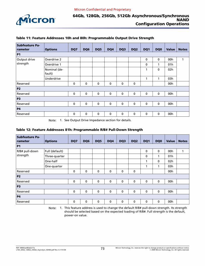
Note: 1. This feature address is used to change the default R/B# pull-down strength. Its strengthshould be selected based on the expected loading of R/B#. Full strength is the default,power-on value.
PDF: 09005aef83d2277aL74A_64Gb_128Gb_256Gb_AsyncSync_NAND.pdf Rev. G 1/14 EN 73 Micron Technology, Inc. reserves the right to change products or specifications without notice.
PDF: 09005aef83d2277aL74A_64Gb_128Gb_256Gb_AsyncSync_NAND.pdf Rev. G 1/14 EN 74 Micron Technology, Inc. reserves the right to change products or specifications without notice.
Status OperationsEach die (LUN) provides its status independently of other die (LUNs) on the same targetthrough its 8-bit status register.
After the READ STATUS (70h) or READ STATUS ENHANCED (78h) command is issued,status register output is enabled. The contents of the status register are returned onDQ[7:0] for each data output request.
When the asynchronous interface is active and status register output is enabled,changes in the status register are seen on DQ[7:0] as long as CE# and RE# are LOW; it isnot necessary to toggle RE# to see the status register update.
When the synchronous interface is active and status register output is enabled, changesin the status register are seen on DQ[7:0] as long as CE# and W/R# are LOW and ALEand CLE are HIGH. DQS also toggles while ALE and CLE are HIGH.
While monitoring the status register to determine when a data transfer from the Flasharray to the data register (tR) is complete, the host must issue the READ MODE (00h)command to disable the status register and enable data output (see READ MODE (00h)(page 85)).
The READ STATUS (70h) command returns the status of the most recently selected die(LUN). To prevent data contention during or following an interleaved die (multi-LUN)operation, the host must enable only one die (LUN) for status output by using the READSTATUS ENHANCED (78h) command (see Interleaved Die (Multi-LUN) Operations(page 110)).
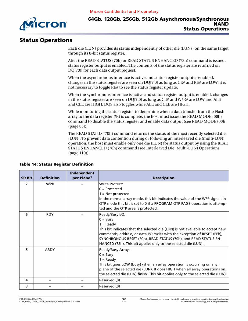
Table 14: Status Register Definition
SR Bit DefinitionIndependent
per Plane1 Description
7 WP# – Write Protect:0 = Protected1 = Not protectedIn the normal array mode, this bit indicates the value of the WP# signal. InOTP mode this bit is set to 0 if a PROGRAM OTP PAGE operation is attemp-ted and the OTP area is protected.
6 RDY – Ready/Busy I/O:0 = Busy1 = ReadyThis bit indicates that the selected die (LUN) is not available to accept newcommands, address, or data I/O cycles with the exception of RESET (FFh),SYNCHRONOUS RESET (FCh), READ STATUS (70h), and READ STATUS EN-HANCED (78h). This bit applies only to the selected die (LUN).
5 ARDY – Ready/Busy Array:0 = Busy1 = ReadyThis bit goes LOW (busy) when an array operation is occurring on anyplane of the selected die (LUN). It goes HIGH when all array operations onthe selected die (LUN) finish. This bit applies only to the selected die (LUN).
PDF: 09005aef83d2277aL74A_64Gb_128Gb_256Gb_AsyncSync_NAND.pdf Rev. G 1/14 EN 75 Micron Technology, Inc. reserves the right to change products or specifications without notice.
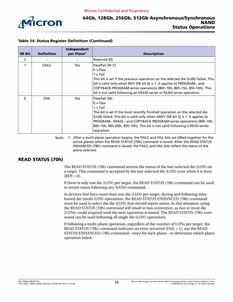
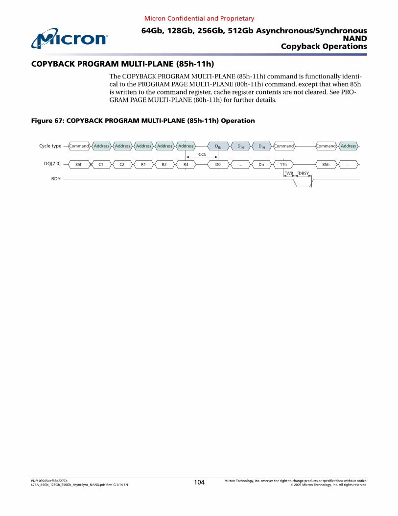
1 FAILC Yes Pass/Fail (N–1):0 = Pass1 = FailThis bit is set if the previous operation on the selected die (LUN) failed. Thisbit is valid only when RDY (SR bit 6) is 1. It applies to PROGRAM-, andCOPYBACK PROGRAM-series operations (80h-10h, 80h-15h, 85h-10h). Thisbit is not valid following an ERASE-series or READ-series operation.
0 FAIL Yes Pass/Fail (N):0 = Pass1 = FailThis bit is set if the most recently finished operation on the selected die(LUN) failed. This bit is valid only when ARDY (SR bit 5) is 1. It applies toPROGRAM-, ERASE-, and COPYBACK PROGRAM-series operations (80h-10h,80h-15h, 60h-D0h, 85h-10h). This bit is not valid following a READ-seriesoperation.
Note: 1. After a multi-plane operation begins, the FAILC and FAIL bits are ORed together for theactive planes when the READ STATUS (70h) command is issued. After the READ STATUSENHANCED (78h) command is issued, the FAILC and FAIL bits reflect the status of theplane selected.
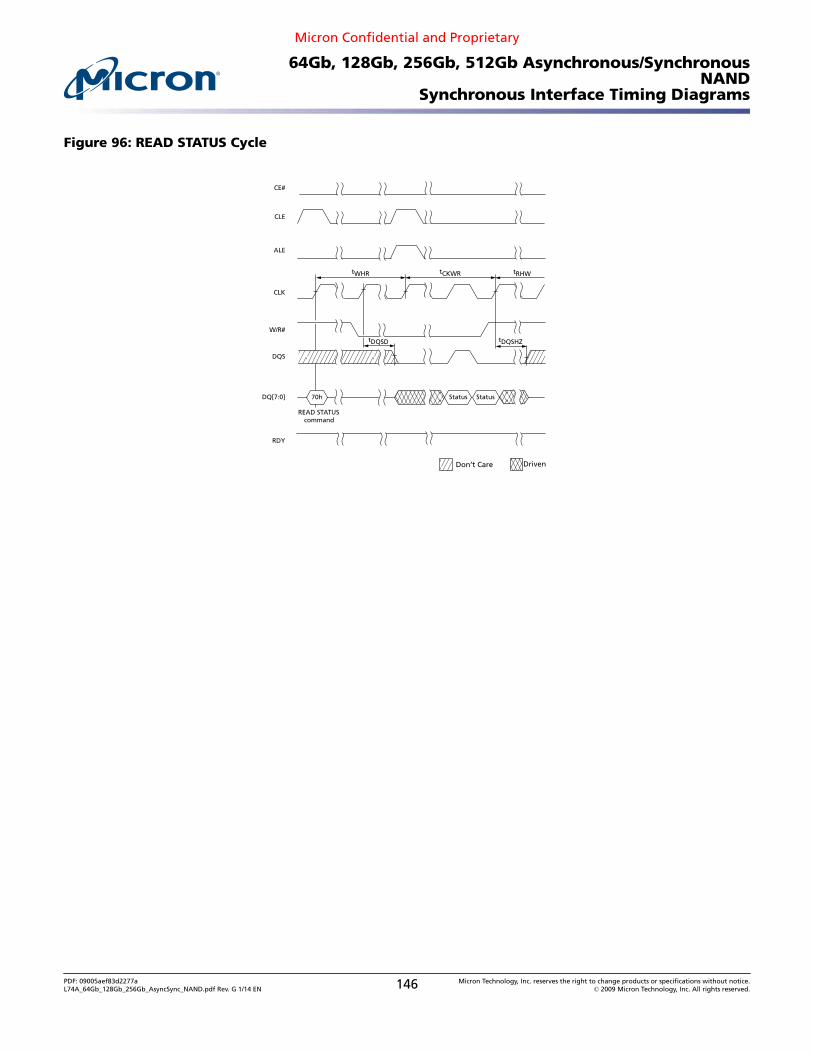
READ STATUS (70h)
The READ STATUS (70h) command returns the status of the last-selected die (LUN) ona target. This command is accepted by the last-selected die (LUN) even when it is busy(RDY = 0).
If there is only one die (LUN) per target, the READ STATUS (70h) command can be usedto return status following any NAND command.
In devices that have more than one die (LUN) per target, during and following inter-leaved die (multi-LUN) operations, the READ STATUS ENHANCED (78h) commandmust be used to select the die (LUN) that should report status. In this situation, usingthe READ STATUS (70h) command will result in bus contention, as two or more die(LUNs) could respond until the next operation is issued. The READ STATUS (70h) com-mand can be used following all single die (LUN) operations.
If following a multi-plane operation, regardless of the number of LUNs per target, theREAD STATUS (70h) command indicates an error occurred (FAIL = 1), use the READSTATUS ENHANCED (78h) command—once for each plane—to determine which planeoperation failed.
PDF: 09005aef83d2277aL74A_64Gb_128Gb_256Gb_AsyncSync_NAND.pdf Rev. G 1/14 EN 76 Micron Technology, Inc. reserves the right to change products or specifications without notice.
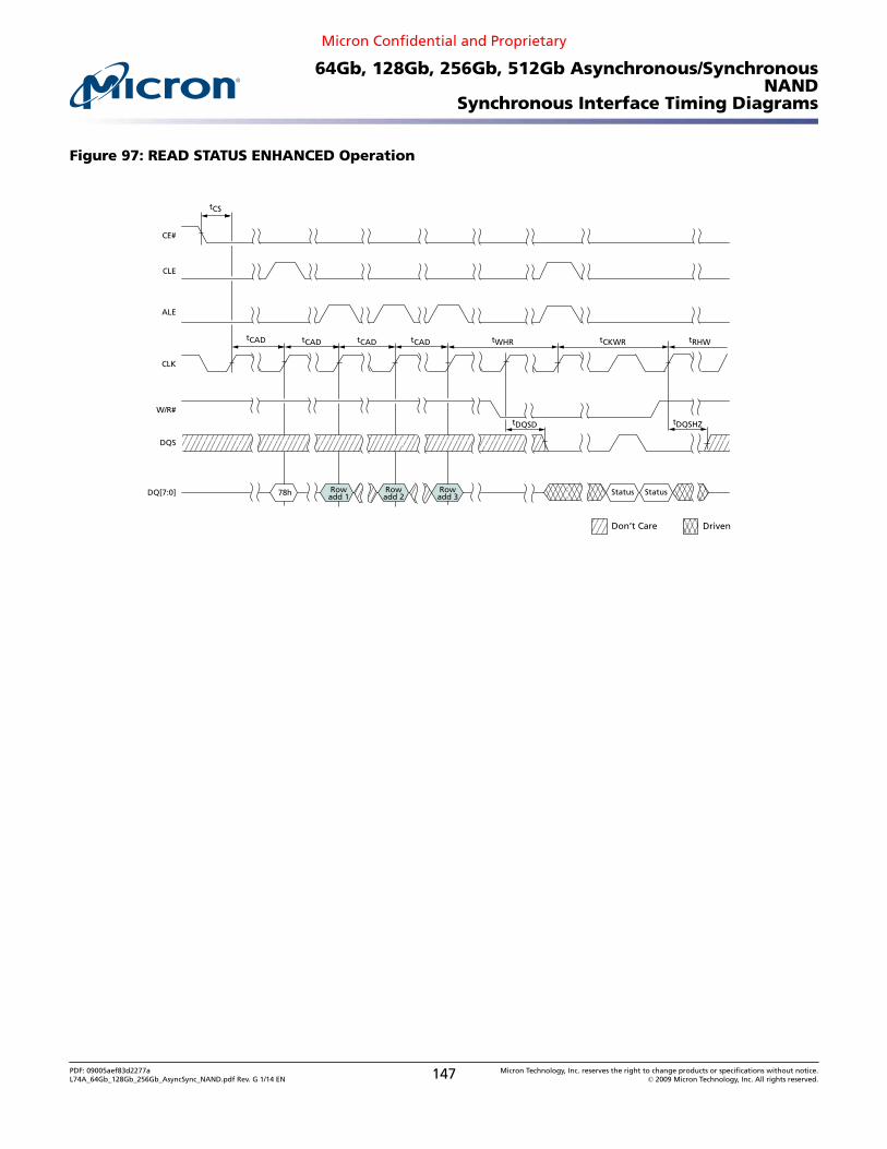
The READ STATUS ENHANCED (78h) command returns the status of the addressed die(LUN) on a target even when it is busy (RDY = 0). This command is accepted by all die(LUNs), even when they are BUSY (RDY = 0).
Writing 78h to the command register, followed by three row address cycles containingthe page, block, and LUN addresses, puts the selected die (LUN) into read status mode.The selected die (LUN) stays in this mode until another valid command is issued. Die(LUNs) that are not addressed are deselected to avoid bus contention.
The selected LUN's status is returned when the host requests data output. The RDY andARDY bits of the status register are shared for all of the planes of the selected die (LUN).The FAILC and FAIL bits are specific to the plane specified in the row address.
The READ STATUS ENHANCED (78h) command also enables the selected die (LUN) fordata output. To begin data output following a READ-series operation after the selecteddie (LUN) is ready (RDY = 1), issue the READ MODE (00h) command, then begin dataoutput. If the host needs to change the cache register that will output data, use theCHANGE READ COLUMN ENHANCED (06h-E0h) command after the die (LUN) isready (see CHANGE READ COLUMN ENHANCED (06h-E0h)).
Use of the READ STATUS ENHANCED (78h) command is prohibited during the power-on RESET (FFh) command and when OTP mode is enabled. It is also prohibited follow-ing some of the other reset, identification, and configuration operations. See individualoperations for specific details.
PDF: 09005aef83d2277aL74A_64Gb_128Gb_256Gb_AsyncSync_NAND.pdf Rev. G 1/14 EN 77 Micron Technology, Inc. reserves the right to change products or specifications without notice.
Column Address OperationsThe column address operations affect how data is input to and output from the cacheregisters within the selected die (LUNs). These features provide host flexibility for man-aging data, especially when the host internal buffer is smaller than the number of databytes or words in the cache register.
When the asynchronous interface is active, column address operations can address anybyte in the selected cache register.
When the synchronous interface is active, column address operations are aligned toword boundaries (CA0 is forced to 0), because as data is transferred on DQ[7:0] in two-byte units.
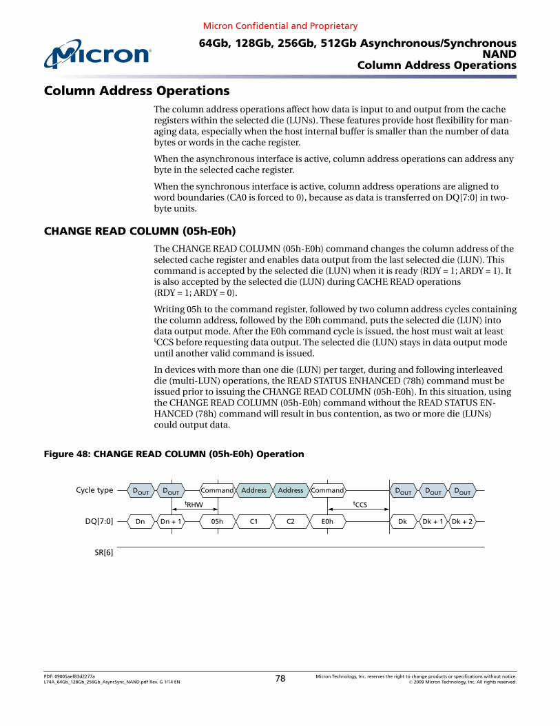
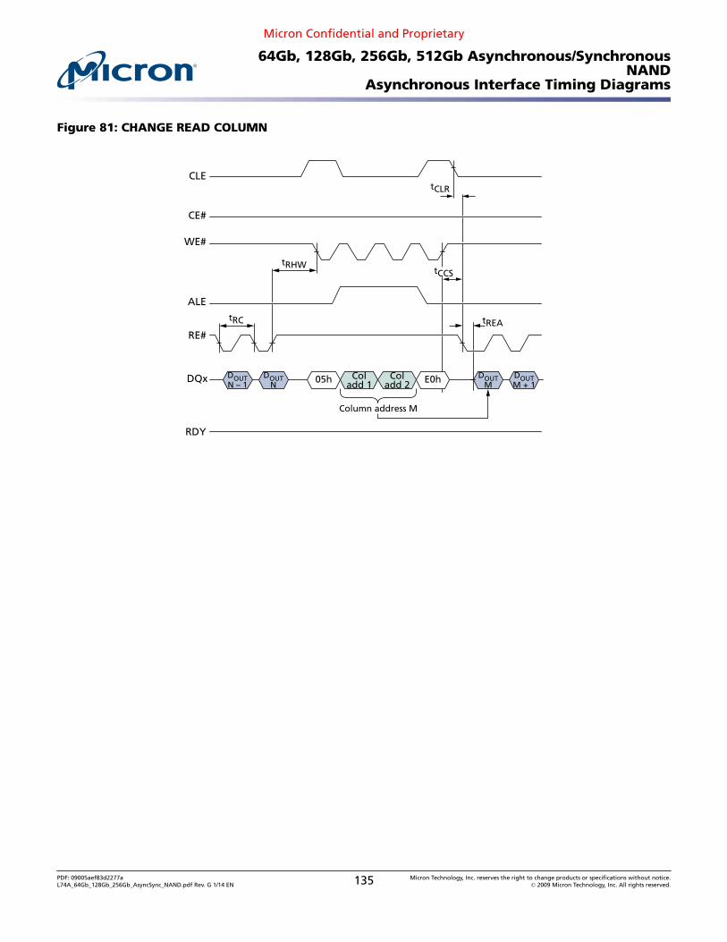
CHANGE READ COLUMN (05h-E0h)
The CHANGE READ COLUMN (05h-E0h) command changes the column address of theselected cache register and enables data output from the last selected die (LUN). Thiscommand is accepted by the selected die (LUN) when it is ready (RDY = 1; ARDY = 1). Itis also accepted by the selected die (LUN) during CACHE READ operations(RDY = 1; ARDY = 0).
Writing 05h to the command register, followed by two column address cycles containingthe column address, followed by the E0h command, puts the selected die (LUN) intodata output mode. After the E0h command cycle is issued, the host must wait at leasttCCS before requesting data output. The selected die (LUN) stays in data output modeuntil another valid command is issued.
In devices with more than one die (LUN) per target, during and following interleaveddie (multi-LUN) operations, the READ STATUS ENHANCED (78h) command must beissued prior to issuing the CHANGE READ COLUMN (05h-E0h). In this situation, usingthe CHANGE READ COLUMN (05h-E0h) command without the READ STATUS EN-HANCED (78h) command will result in bus contention, as two or more die (LUNs)could output data.
PDF: 09005aef83d2277aL74A_64Gb_128Gb_256Gb_AsyncSync_NAND.pdf Rev. G 1/14 EN 78 Micron Technology, Inc. reserves the right to change products or specifications without notice.
The CHANGE READ COLUMN ENHANCED (06h-E0h) command enables data outputon the addressed die’s (LUN’s) cache register at the specified column address. Thiscommand is accepted by a die (LUN) when it is ready (RDY = 1; ARDY = 1).
Writing 06h to the command register, followed by two column address cycles and threerow address cycles, followed by E0h, enables data output mode on the address LUN’scache register at the specified column address. After the E0h command cycle is issued,the host must wait at least tCCS before requesting data output. The selected die (LUN)stays in data output mode until another valid command is issued.
Following a multi-plane read page operation, the CHANGE READ COLUMN EN-HANCED (06h-E0h) command is used to select the cache register to be enabled for dataoutput. After data output is complete on the selected plane, the command can be is-sued again to begin data output on another plane.
In devices with more than one die (LUN) per target, after all of the die (LUNs) on thetarget are ready (RDY = 1), the CHANGE READ COLUMN ENHANCED (06h-E0h) com-mand can be used following an interleaved die (multi-LUN) read operation. Die (LUNs)that are not addressed are deselected to avoid bus contention.
In devices with more than one die (LUN) per target, during interleaved die (multi-LUN)operations where more than one or more die (LUNs) are busy (RDY = 1; ARDY = 0 orRDY = 0; ARDY = 0), the READ STATUS ENHANCED (78h) command must be issued tothe die (LUN) to be selected prior to issuing the CHANGE READ COLUMN ENHANCED(06h-E0h). In this situation, using the CHANGE READ COLUMN ENHANCED (06h-E0h)command without the READ STATUS ENHANCED (78h) command will result in buscontention, as two or more die (LUNs) could output data.
If there is a need to update the column address without selecting a new cache registeror LUN, the CHANGE READ COLUMN (05h-E0h) command can be used instead.
PDF: 09005aef83d2277aL74A_64Gb_128Gb_256Gb_AsyncSync_NAND.pdf Rev. G 1/14 EN 79 Micron Technology, Inc. reserves the right to change products or specifications without notice.
The CHANGE WRITE COLUMN (85h) command changes the column address of the se-lected cache register and enables data input on the last-selected die (LUN). This com-mand is accepted by the selected die (LUN) when it is ready (RDY = 1; ARDY = 1). It isalso accepted by the selected die (LUN) during cache program operations(RDY = 1; ARDY = 0).
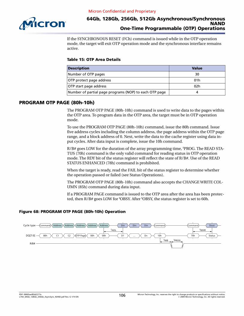
Writing 85h to the command register, followed by two column address cycles containingthe column address, puts the selected die (LUN) into data input mode. After the secondaddress cycle is issued, the host must wait at least tCCS before inputting data. The selec-ted die (LUN) stays in data input mode until another valid command is issued. Thoughdata input mode is enabled, data input from the host is optional. Data input begins atthe column address specified.
The CHANGE WRITE COLUMN (85h) command is allowed after the required addresscycles are specified, but prior to the final command cycle (10h, 11h, 15h) of the follow-ing commands while data input is permitted: PROGRAM PAGE (80h-10h), PROGRAMPAGE MULTI-PLANE (80h-11h), PROGRAM PAGE CACHE (80h-15h), COPYBACK PRO-GRAM (85h-10h), and COPYBACK PROGRAM MULTI-PLANE (85h-11h).
In devices that have more than one die (LUN) per target, the CHANGE WRITE COLUMN(85h) command can be used with other commands that support interleaved die (multi-LUN) operations.
PDF: 09005aef83d2277aL74A_64Gb_128Gb_256Gb_AsyncSync_NAND.pdf Rev. G 1/14 EN 80 Micron Technology, Inc. reserves the right to change products or specifications without notice.
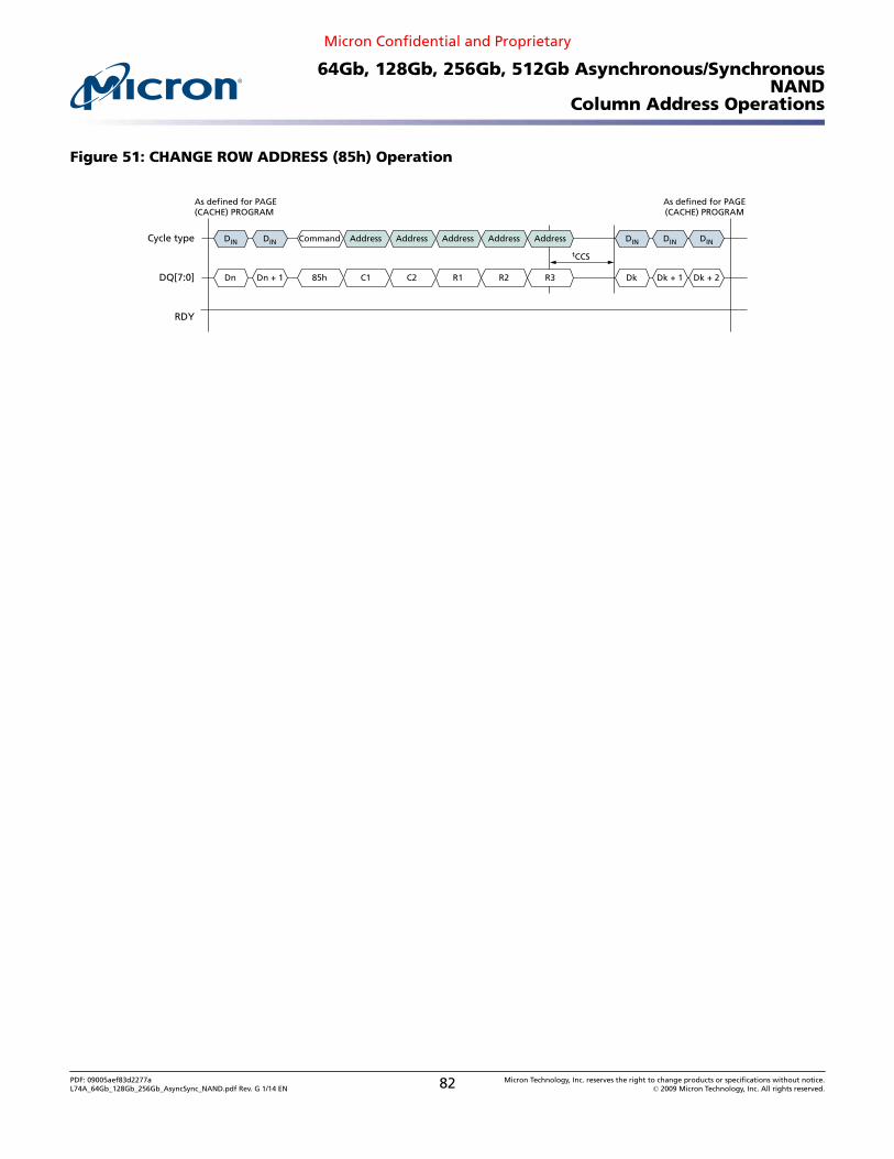
The CHANGE ROW ADDRESS (85h) command changes the row address (block andpage) where the cache register contents will be programmed in the NAND Flash array. Italso changes the column address of the selected cache register and enables data inputon the specified die (LUN). This command is accepted by the selected die (LUN) whenit is ready (RDY = 1; ARDY = 1). It is also accepted by the selected die (LUN) during cacheprogramming operations (RDY = 1; ARDY = 0).
Write 85h to the command register. Then write two column address cycles and threerow address cycles. This updates the page and block destination of the selected planefor the addressed LUN and puts the cache register into data input mode. After the fifthaddress cycle is issued the host must wait at least tCCS before inputting data. The selec-ted LUN stays in data input mode until another valid command is issued. Though datainput mode is enabled, data input from the host is optional. Data input begins at thecolumn address specified.
The CHANGE ROW ADDRESS (85h) command is allowed after the required address cy-cles are specified, but prior to the final command cycle (10h, 11h, 15h) of the followingcommands while data input is permitted: PROGRAM PAGE (80h-10h), PROGRAM PAGEMULTI-PLANE (80h-11h), PROGRAM PAGE CACHE (80h-15h), COPYBACK PROGRAM(85h-10h), and COPYBACK PROGRAM MULTI-PLANE (85h-11h). When used with thesecommands, the LUN address and plane select bits are required to be identical to theLUN address and plane select bits originally specified.
The CHANGE ROW ADDRESS (85h) command enables the host to modify the originalpage and block address for the data in the cache register to a new page and block ad-dress.
In devices that have more than one die (LUN) per target, the CHANGE ROW ADDRESS(85h) command can be used with other commands that support interleaved die (multi-LUN) operations.
The CHANGE ROW ADDRESS (85h) command can be used with the CHANGE READCOLUMN (05h-E0h) or CHANGE READ COLUMN ENHANCED (06h-E0h) commands toread and modify cache register contents in small sections prior to programming cacheregister contents to the NAND Flash array. This capability can reduce the amount ofbuffer memory used in the host controller.
To modify the cache register contents in small sections, first issue a PAGE READ(00h-30h) or COPYBACK READ (00h-35h) operation. When data output is enabled, thehost can output a portion of the cache register contents. To modify the cache registercontents, issue the 85h command, the column and row addresses, and input the newdata. The host can re-enable data output by issuing the 11h command, waiting tDBSY,and then issuing the CHANGE READ COLUMN (05h-E0h) or CHANGE READ COLUMNENHANCED (06h-E0h) command. It is possible toggle between data output and datainput multiple times. After the final CHANGE ROW ADDRESS (85h) operation is com-plete, issue the 10h command to program the cache register to the NAND Flash array.
PDF: 09005aef83d2277aL74A_64Gb_128Gb_256Gb_AsyncSync_NAND.pdf Rev. G 1/14 EN 81 Micron Technology, Inc. reserves the right to change products or specifications without notice.
PDF: 09005aef83d2277aL74A_64Gb_128Gb_256Gb_AsyncSync_NAND.pdf Rev. G 1/14 EN 82 Micron Technology, Inc. reserves the right to change products or specifications without notice.
Read OperationsRead operations are used to copy data from the NAND Flash array of one or more of theplanes to their respective cache registers and to enable data output from the cache reg-isters to the host through the DQ bus.
Read Operations
The READ PAGE (00h-30h) command, when issued by itself, reads one page from theNAND Flash array to its cache register and enables data output for that cache register.
During data output the following commands can be used to read and modify the data inthe cache registers: CHANGE READ COLUMN (05h-E0h) and CHANGE ROW ADDRESS(85h).
Read Cache Operations
To increase data throughput, the READ PAGE CACHE-series (31h, 00h-31h) commandscan be used to output data from the cache register while concurrently copying a pagefrom the NAND Flash array to the data register.
To begin a read page cache sequence, begin by reading a page from the NAND Flash ar-ray to its corresponding cache register using the READ PAGE (00h-30h) command.R/B# goes LOW during tR and the selected die (LUN) is busy (RDY = 0, ARDY = 0). AftertR (R/B# is HIGH and RDY = 1, ARDY = 1), issue either of these commands:
• READ PAGE CACHE SEQUENTIAL (31h)—copies the next sequential page from theNAND Flash array to the data register
• READ PAGE CACHE RANDOM (00h-31h)—copies the page specified in this commandfrom the NAND Flash array (any plane) to its corresponding data register
After the READ PAGE CACHE-series (31h, 00h-31h) command has been issued, R/B#goes LOW on the target, and RDY = 0 and ARDY = 0 on the die (LUN) for tRCBSY whilethe next page begins copying data from the array to the data register. After tRCBSY,R/B# goes HIGH and the die’s (LUN’s) status register bits indicate the device is busywith a cache operation (RDY = 1, ARDY = 0). The cache register becomes available andthe page requested in the READ PAGE CACHE operation is transferred to the data regis-ter. At this point, data can be output from the cache register, beginning at column ad-dress 0. The CHANGE READ COLUMN (05h-E0h) command can be used to change thecolumn address of the data output by the die (LUN).
After outputting the desired number of bytes from the cache register, either an addi-tional READ PAGE CACHE-series (31h, 00h-31h) operation can be started or the READPAGE CACHE LAST (3Fh) command can be issued.
If the READ PAGE CACHE LAST (3Fh) command is issued, R/B# goes LOW on the target,and RDY = 0 and ARDY = 0 on the die (LUN) for tRCBSY while the data register is copiedinto the cache register. After tRCBSY, R/B# goes HIGH and RDY = 1 andARDY = 1, indicating that the cache register is available and that the die (LUN) is ready.Data can then be output from the cache register, beginning at column address 0. TheCHANGE READ COLUMN (05h-E0h) command can be used to change the column ad-dress of the data being output.
For READ PAGE CACHE-series (31h, 00h-31h, 3Fh), during the die (LUN) busy time,tRCBSY, when RDY = 0 and ARDY = 0, the only valid commands are status operations(70h, 78h) and RESET (FFh, FCh). When RDY = 1 and ARDY = 0, the only valid com-mands during READ PAGE CACHE-series (31h, 00h-31h) operations are status opera-
PDF: 09005aef83d2277aL74A_64Gb_128Gb_256Gb_AsyncSync_NAND.pdf Rev. G 1/14 EN 83 Micron Technology, Inc. reserves the right to change products or specifications without notice.
Multi-plane read page operations improve data throughput by copying data from morethan one plane simultaneously to the specified cache registers. This is done by pre-pending one or more READ PAGE MULTI-PLANE (00h-32h) commands in front of theREAD PAGE (00h-30h) command.
When the die (LUN) is ready, the CHANGE READ COLUMN ENHANCED (06h-E0h)command determines which plane outputs data. During data output, the followingcommands can be used to read and modify the data in the cache registers: CHANGEREAD COLUMN (05h-E0h) and CHANGE ROW ADDRESS (85h). See Multi-Plane Opera-tions for details.
Multi-Plane Read Cache Operations
Multi-plane read cache operations can be used to output data from more than onecache register while concurrently copying one or more pages from the NAND Flash ar-ray to the data register. This is done by prepending READ PAGE MULTI-PLANE(00h-32h) commands in front of the PAGE READ CACHE RANDOM (00h-31h) com-mand.
To begin a multi-plane read page cache sequence, begin by issuing a MULTI-PLANEREAD PAGE operation using the READ PAGE MULTI-PLANE (00h-32h) and READ PAGE(00h-30h) commands. R/B# goes LOW during tR and the selected die (LUN) is busy(RDY = 0, ARDY = 0). After tR (R/B# is HIGH and RDY = 1, ARDY = 1), issue either of thesecommands:
• READ PAGE CACHE SEQUENTIAL (31h)—copies the next sequential page from thepreviously addressed planes from the NAND Flash array to the data registers.
• READ PAGE MULTI-PLANE (00h-32h) commands, if desired, followed by the READPAGE CACHE RANDOM (00h-31h) command—copies the pages specified from theNAND Flash array to the corresponding data registers.
After the READ PAGE CACHE-series (31h, 00h-31h) command has been issued, R/B#goes LOW on the target, and RDY = 0 and ARDY = 0 on the die (LUN) for tRCBSY whilethe next pages begin copying data from the array to the data registers. After tRCBSY,R/B# goes HIGH and the LUN’s status register bits indicate the device is busy with acache operation (RDY = 1, ARDY = 0). The cache registers become available and the pa-ges requested in the READ PAGE CACHE operation are transferred to the data registers.Issue the CHANGE READ COLUMN ENHANCED (06h-E0h) command to determinewhich cache register will output data. After data is output, the CHANGE READ COL-UMN ENHANCED (06h-E0h) command can be used to output data from other cacheregisters. After a cache register has been selected, the CHANGE READ COLUMN (05h-E0h) command can be used to change the column address of the data output.
After outputting data from the cache registers, either an additional MULTI-PLANEREAD CACHE-series (31h, 00h-31h) operation can be started or the READ PAGE CACHELAST (3Fh) command can be issued.
If the READ PAGE CACHE LAST (3Fh) command is issued, R/B# goes LOW on the target,and RDY = 0 and ARDY = 0 on the die (LUN) for tRCBSY while the data registers are cop-ied into the cache registers. After tRCBSY, R/B# goes HIGH and RDY = 1 and ARDY = 1,indicating that the cache registers are available and that the die (LUN) is ready. Issue the
PDF: 09005aef83d2277aL74A_64Gb_128Gb_256Gb_AsyncSync_NAND.pdf Rev. G 1/14 EN 84 Micron Technology, Inc. reserves the right to change products or specifications without notice.
CHANGE READ COLUMN ENHANCED (06h-E0h) command to determine which cacheregister will output data. After data is output, the CHANGE READ COLUMN EN-HANCED (06h-E0h) command can be used to output data from other cache registers.After a cache register has been selected, the CHANGE READ COLUMN (05h-E0h) com-mand can be used to change the column address of the data output.
For READ PAGE CACHE-series (31h, 00h-31h, 3Fh), during the die (LUN) busy time,tRCBSY, when RDY = 0 and ARDY = 0, the only valid commands are status operations(70h, 78h) and RESET (FFh, FCh). When RDY = 1 and ARDY = 0, the only valid com-mands during READ PAGE CACHE-series (31h, 00h-31h) operations are status opera-tions (70h, 78h), READ MODE (00h), multi-plane read cache-series (31h, 00h-32h,00h-31h), CHANGE READ COLUMN (05h-E0h, 06h-E0h), and RESET (FFh, FCh).
See Multi-Plane Operations for additional multi-plane addressing requirements.
READ MODE (00h)
The READ MODE (00h) command disables status output and enables data output forthe last-selected die (LUN) and cache register after a READ operation (00h-30h,00h-35h) has been monitored with a status operation (70h, 78h). This command is ac-cepted by the die (LUN) when it is ready (RDY = 1, ARDY = 1). It is also accepted by thedie (LUN) during READ PAGE CACHE (31h, 3Fh, 00h-31h) operations(RDY = 1 and ARDY = 0).
In devices that have more than one die (LUN) per target, during and following inter-leaved die (multi-LUN) operations, the READ STATUS ENHANCED (78h) commandmust be used to select only one die (LUN) prior to issuing the READ MODE (00h) com-mand. This prevents bus contention.
PDF: 09005aef83d2277aL74A_64Gb_128Gb_256Gb_AsyncSync_NAND.pdf Rev. G 1/14 EN 85 Micron Technology, Inc. reserves the right to change products or specifications without notice.
The READ PAGE (00h–30h) command copies a page from the NAND Flash array to itsrespective cache register and enables data output. This command is accepted by the die(LUN) when it is ready (RDY = 1, ARDY = 1).
To read a page from the NAND Flash array, write the 00h command to the commandregister, the write five address cycles to the address registers, and conclude with the 30hcommand. The selected die (LUN) will go busy (RDY = 0, ARDY = 0) for tR as data istransferred.
To determine the progress of the data transfer, the host can monitor the target's R/B#signal or, alternatively, the status operations (70h, 78h) can be used. If the status opera-tions are used to monitor the LUN's status, when the die (LUN) is ready(RDY = 1, ARDY = 1), the host disables status output and enables data output by issuingthe READ MODE (00h) command. When the host requests data output, output beginsat the column address specified.
During data output the CHANGE READ COLUMN (05h-E0h) command can be issued.
In devices that have more than one die (LUN) per target, during and following inter-leaved die (multi-LUN) operations the READ STATUS ENHANCED (78h) commandmust be used to select only one die (LUN) prior to the issue of the READ MODE (00h)command. This prevents bus contention.
The READ PAGE (00h-30h) command is used as the final command of a multi-planeread operation. It is preceded by one or more READ PAGE MULTI-PLANE (00h-32h)commands. Data is transferred from the NAND Flash array for all of the addressedplanes to their respective cache registers. When the die (LUN) is ready(RDY = 1, ARDY = 1), data output is enabled for the cache register linked to the last evenplane addressed. When the host requests data output, output begins at the column ad-dress last specified in the READ PAGE (00h-30h) command. The CHANGE READ COL-UMN ENHANCED (06h-E0h) command is used to enable data output in the othercache registers. See Multi-Plane Operations for additional multi-plane addressing re-quirements.
PDF: 09005aef83d2277aL74A_64Gb_128Gb_256Gb_AsyncSync_NAND.pdf Rev. G 1/14 EN 86 Micron Technology, Inc. reserves the right to change products or specifications without notice.
The READ PAGE CACHE SEQUENTIAL (31h) command reads the next sequential pagewithin a block into the data register while the previous page is output from the cacheregister. This command is accepted by the die (LUN) when it is ready(RDY = 1, ARDY = 1). It is also accepted by the die (LUN) during READ PAGE CACHE(31h, 00h-31h) operations (RDY = 1 and ARDY = 0).
To issue this command, write 31h to the command register. After this command is is-sued, R/B# goes LOW and the die (LUN) is busy (RDY = 0, ARDY = 0) for tRCBSY. AftertRCBSY, R/B# goes HIGH and the die (LUN) is busy with a cache operation(RDY = 1, ARDY = 0), indicating that the cache register is available and that the specifiedpage is copying from the NAND Flash array to the data register. At this point, data canbe output from the cache register beginning at column address 0. The CHANGE READCOLUMN (05h-E0h) command can be used to change the column address of the databeing output from the cache register.
The READ PAGE CACHE SEQUENTIAL (31h) command can be used to cross blockboundaries. If the READ PAGE CACHE SEQUENTIAL (31h) command is issued after thelast page of a block is read into the data register, the next page read will be the next logi-cal block in the plane which the 31h command was issued. Do not issue the READ PAGECACHE SEQUENTIAL (31h) to cross die (LUN) boundaries. Instead, issue the READPAGE CACHE LAST (3Fh) command.
If the READ PAGE CACHE SEQUENTIAL (31h) command is issued after a MULTI-PLANE READ PAGE operation (00h-32h, 00h-30h), the next sequential pages are readinto the data registers while the previous pages can be output from the cache registers.After the die (LUN) is ready (RDY = 1, ARDY = 0), the CHANGE READ COLUMN EN-HANCED (06h-E0h) command is used to select which cache register outputs data.
PDF: 09005aef83d2277aL74A_64Gb_128Gb_256Gb_AsyncSync_NAND.pdf Rev. G 1/14 EN 87 Micron Technology, Inc. reserves the right to change products or specifications without notice.
The READ PAGE CACHE RANDOM (00h-31h) command reads the specified block andpage into the data register while the previous page is output from the cache register.This command is accepted by the die (LUN) when it is ready (RDY = 1, ARDY = 1). It isalso accepted by the die (LUN) during READ PAGE CACHE (31h, 00h-31h) operations(RDY = 1 and ARDY = 0).
To issue this command, write 00h to the command register, then write five address cy-cles to the address register, and conclude by writing 31h to the command register. Thecolumn address in the address specified is ignored. The die (LUN) address must matchthe same die (LUN) address as the previous READ PAGE (00h-30h) command or, if ap-plicable, the previous READ PAGE CACHE RANDOM (00h-31h) command. There is norestriction on the plane address.
After this command is issued, R/B# goes LOW and the die (LUN) is busy(RDY = 0, ARDY = 0) for tRCBSY. After tRCBSY, R/B# goes HIGH and the die (LUN) is busywith a cache operation (RDY = 1, ARDY = 0), indicating that the cache register is availa-ble and that the specified page is copying from the NAND Flash array to the data regis-ter. At this point, data can be output from the cache register beginning at column ad-dress 0. The CHANGE READ COLUMN (05h-E0h) command can be used to change thecolumn address of the data being output from the cache register.
In devices that have more than one die (LUN) per target, during and following inter-leaved die (multi-LUN) operations the READ STATUS ENHANCED (78h) command fol-lowed by the READ MODE (00h) command must be used to select only one die (LUN)and prevent bus contention.
If a MULTI-PLANE CACHE RANDOM (00h-32h, 00h-31h) command is issued after aMULTI-PLANE READ PAGE operation (00h-32h, 00h-30h), then the addressed pages areread into the data registers while the previous pages can be output from the cache regis-ters. After the die (LUN) is ready (RDY = 1, ARDY = 0), the CHANGE READ COLUMN EN-HANCED (06h-E0h) command is used to select which cache register outputs data.
PDF: 09005aef83d2277aL74A_64Gb_128Gb_256Gb_AsyncSync_NAND.pdf Rev. G 1/14 EN 88 Micron Technology, Inc. reserves the right to change products or specifications without notice.
PDF: 09005aef83d2277aL74A_64Gb_128Gb_256Gb_AsyncSync_NAND.pdf Rev. G 1/14 EN 89 Micron Technology, Inc. reserves the right to change products or specifications without notice.
The READ PAGE CACHE LAST (3Fh) command ends the read page cache sequence andcopies a page from the data register to the cache register. This command is accepted bythe die (LUN) when it is ready (RDY = 1, ARDY = 1). It is also accepted by the die (LUN)during READ PAGE CACHE (31h, 00h-31h) operations (RDY = 1 and ARDY = 0).
To issue the READ PAGE CACHE LAST (3Fh) command, write 3Fh to the command reg-ister. After this command is issued, R/B# goes LOW and the die (LUN) is busy(RDY = 0, ARDY = 0) for tRCBSY. After tRCBSY, R/B# goes HIGH and the die (LUN) isready (RDY = 1, ARDY = 1). At this point, data can be output from the cache register, be-ginning at column address 0. The CHANGE READ COLUMN (05h-E0h) command canbe used to change the column address of the data being output from the cache register.
In devices that have more than one LUN per target, during and following interleaved die(multi-LUN) operations the READ STATUS ENHANCED (78h) command followed bythe READ MODE (00h) command must be used to select only one die (LUN) and pre-vent bus contention.
If the READ PAGE CACHE LAST (3Fh) command is issued after a MULTI-PLANE READPAGE CACHE operation (31h; 00h-32h, 00h-30h), the die (LUN) goes busy until the pa-ges are copied from the data registers to the cache registers. After the die (LUN) is ready(RDY = 1, ARDY = 1), the CHANGE READ COLUMN ENHANCED (06h-E0h) command isused to select which cache register outputs data.
PDF: 09005aef83d2277aL74A_64Gb_128Gb_256Gb_AsyncSync_NAND.pdf Rev. G 1/14 EN 90 Micron Technology, Inc. reserves the right to change products or specifications without notice.
The READ PAGE MULTI-PLANE (00h-32h) command queues a plane to transfer datafrom the NAND flash array to its cache register. This command can be issued one ormore times. Each time a new plane address is specified, that plane is also queued fordata transfer. The READ PAGE (00h-30h) command is issued to select the final planeand to begin the read operation for all previously queued planes. All queued planes willtransfer data from the NAND Flash array to their cache registers.
To issue the READ PAGE MULTI-PLANE (00h-32h) command, write 00h to the com-mand register, then write five address cycles to the address register, and conclude bywriting 32h to the command register. The column address in the address specified is ig-nored.
After this command is issued, R/B# goes LOW and the die (LUN) is busy(RDY = 0, ARDY = 0) for tDBSY. After tDBSY, R/B# goes HIGH and the die (LUN) is ready(RDY = 1, ARDY = 1). At this point, the die (LUN) and block are queued for data transferfrom the array to the cache register for the addressed plane. During tDBSY, the only val-id commands are status operations (70h, 78h) and reset commands (FFh, FCh). Follow-ing tDBSY, to continue the MULTI-PLANE READ operation, the only valid commandsare status operations (70h, 78h), READ PAGE MULTI-PLANE (00h-32h), READ PAGE(00h-30h), and READ PAGE CACHE RANDOM (00h-31h).
Additional READ PAGE MULTI-PLANE (00h-32h) commands can be issued to queue ad-ditional planes for data transfer.
If the READ PAGE (00h-30h) command is used as the final command of a MULTI-PLANE READ operation, data is transferred from the NAND Flash array for all of the ad-dressed planes to their respective cache registers. When the die (LUN) is ready(RDY = 1, ARDY = 1), data output is enabled for the cache register linked to the last evenplane addressed. When the host requests data output, it begins at the column addressspecified in the READ PAGE (00h-30h) command. To enable data output in the othercache registers, use the CHANGE READ COLUMN ENHANCED (06h-E0h) command.Additionally, the CHANGE READ COLUMN (05h-E0h) command can be used to changethe column address within the currently selected plane.
If the READ PAGE CACHE SEQUENTIAL (31h) is used as the final command of a MUL-TI-PLANE READ CACHE operation, data is copied from the previously read operationfrom each plane to each cache register and then data is transferred from the NANDFlash array for all previously addressed planes to their respective data registers. Whenthe die (LUN) is ready (RDY = 1, ARDY = 0), data output is enabled. The CHANGE READCOLUMN ENHANCED (06h-E0h) command is used to determine which cache registeroutputs data first. To enable data output in the other cache registers, use the CHANGEREAD COLUMN ENHANCED (06h-E0h) command. Additionally, the CHANGE READCOLUMN (05h-E0h) command can be used to change the column address within thecurrently selected plane.
If the READ PAGE CACHE RANDOM (00h-31h) command is used as the final commandof a MULTI-PLANE READ CACHE operation, data is copied from the previously read op-eration from the data register to the cache register and then data is transferred from theNAND Flash array for all of the addressed planes to their respective data registers. Whenthe die (LUN) is ready (RDY = 1, ARDY = 0), data output is enabled. The CHANGE READCOLUMN ENHANCED (06h-E0h) command is used to determine which cache registeroutputs data first. To enable data output in the other cache registers, use the CHANGEREAD COLUMN ENHANCED (06h-E0h) command. Additionally, the CHANGE READ
PDF: 09005aef83d2277aL74A_64Gb_128Gb_256Gb_AsyncSync_NAND.pdf Rev. G 1/14 EN 91 Micron Technology, Inc. reserves the right to change products or specifications without notice.
PDF: 09005aef83d2277aL74A_64Gb_128Gb_256Gb_AsyncSync_NAND.pdf Rev. G 1/14 EN 92 Micron Technology, Inc. reserves the right to change products or specifications without notice.
Program OperationsProgram operations are used to move data from the cache or data registers to the NANDarray of one or more planes. During a program operation the contents of the cacheand/or data registers are modified by the internal control logic.
Within a block, pages must be programmed sequentially from the least significant pageaddress to the most significant page address (i.e. 0, 1, 2, 3, …). Programming pages outof order within a block is prohibited.
Program Operations
The PROGRAM PAGE (80h-10h) command, when not preceded by the PROGRAM PAGEMULTI-PLANE (80h-11h) command, programs one page from the cache register to theNAND Flash array. When the die (LUN) is ready (RDY = 1, ARDY = 1), the host shouldcheck the FAIL bit to verify that the operation has completed successfully.
Program Cache Operations
The PROGRAM PAGE CACHE (80h-15h) command can be used to improve program op-eration system performance. When this command is issued, the die (LUN) goes busy(RDY = 0, ARDY = 0) while the cache register contents are copied to the data register,and the die (LUN) is busy with a program cache operation (RDY = 1, ARDY = 0). Whilethe contents of the data register are moved to the NAND Flash array, the cache registeris available for an additional PROGRAM PAGE CACHE (80h-15h) or PROGRAM PAGE(80h-10h) command.
For PROGRAM PAGE CACHE-series (80h-15h) operations, during the die (LUN) busytimes, tCBSY and tLPROG, when RDY = 0 and ARDY = 0, the only valid commands arestatus operations (70h, 78h) and reset (FFh, FCh). When RDY = 1 and ARDY = 0, the onlyvalid commands during PROGRAM PAGE CACHE-series (80h-15h) operations are statusoperations (70h, 78h), PROGRAM PAGE CACHE (80h-15h), PROGRAM PAGE (80h-10h),CHANGE WRITE COLUMN (85h), CHANGE ROW ADDRESS (85h), and reset (FFh, FCh).
Multi-Plane Program Operations
The PROGRAM PAGE MULTI-PLANE (80h-11h) command can be used to improve pro-gram operation system performance by enabling multiple pages to be moved from thecache registers to different planes of the NAND Flash array. This is done by prependingone or more PROGRAM PAGE MULTI-PLANE (80h-11h) commands in front of the PRO-GRAM PAGE (80h-10h) command. See Multi-Plane Operations for details.
Multi-Plane Program Cache Operations
The PROGRAM PAGE MULTI-PLANE (80h-11h) command can be used to improve pro-gram cache operation system performance by enabling multiple pages to be movedfrom the cache registers to the data registers and, while the pages are being transferredfrom the data registers to different planes of the NAND Flash array, free the cache regis-ters to receive data input from the host. This is done by prepending one or more PRO-GRAM PAGE MULTI-PLANE (80h-11h) commands in front of the PROGRAM PAGECACHE (80h-15h) command. See Multi-Plane Operations for details.
PROGRAM PAGE (80h-10h)
The PROGRAM PAGE (80h-10h) command enables the host to input data to a cache reg-ister, and moves the data from the cache register to the specified block and page ad-dress in the array of the selected die (LUN). This command is accepted by the die (LUN)
PDF: 09005aef83d2277aL74A_64Gb_128Gb_256Gb_AsyncSync_NAND.pdf Rev. G 1/14 EN 93 Micron Technology, Inc. reserves the right to change products or specifications without notice.
when it is ready (RDY = 1, ARDY = 1). It is also accepted by the die (LUN) when it is busywith a PROGRAM PAGE CACHE (80h-15h) operation (RDY = 1, ARDY = 0).
To input a page to the cache register and move it to the NAND array at the block andpage address specified, write 80h to the command register. Unless this command hasbeen preceded by a PROGRAM PAGE MULTI-PLANE (80h-11h) command, issuing the80h to the command register clears all of the cache registers' contents on the selectedtarget. Then write five address cycles containing the column address and row address.Data input cycles follow. Serial data is input beginning at the column address specified.At any time during the data input cycle the CHANGE WRITE COLUMN (85h) andCHANGE ROW ADDRESS (85h) commands may be issued. When data input is com-plete, write 10h to the command register. The selected LUN will go busy(RDY = 0, ARDY = 0) for tPROG as data is transferred.
To determine the progress of the data transfer, the host can monitor the target's R/B#signal or, alternatively, the status operations (70h, 78h) may be used. When the die(LUN) is ready (RDY = 1, ARDY = 1), the host should check the status of the FAIL bit.
In devices that have more than one die (LUN) per target, during and following inter-leaved die (multi-LUN) operations, the READ STATUS ENHANCED (78h) commandmust be used to select only one die (LUN) for status output. Use of the READ STATUS(70h) command could cause more than one die (LUN) to respond, resulting in bus con-tention.
The PROGRAM PAGE (80h-10h) command is used as the final command of a multi-plane program operation. It is preceded by one or more PROGRAM PAGE MULTI-PLANE (80h-11h) commands. Data is transferred from the cache registers for all of theaddressed planes to the NAND array. The host should check the status of the operationby using the status operations (70h, 78h). See Multi-Plane Operations for multi-planeaddressing requirements.
PDF: 09005aef83d2277aL74A_64Gb_128Gb_256Gb_AsyncSync_NAND.pdf Rev. G 1/14 EN 94 Micron Technology, Inc. reserves the right to change products or specifications without notice.
The PROGRAM PAGE CACHE (80h-15h) command enables the host to input data to acache register; copies the data from the cache register to the data register; then movesthe data register contents to the specified block and page address in the array of the se-lected die (LUN). After the data is copied to the data register, the cache register is availa-ble for additional PROGRAM PAGE CACHE (80h-15h) or PROGRAM PAGE (80h-10h)commands. The PROGRAM PAGE CACHE (80h-15h) command is accepted by the die(LUN) when it is ready (RDY =1, ARDY = 1). It is also accepted by the die (LUN) whenbusy with a PROGRAM PAGE CACHE (80h-15h) operation (RDY = 1, ARDY = 0).
To input a page to the cache register to move it to the NAND array at the block and pageaddress specified, write 80h to the command register. Unless this command has beenpreceded by a PROGRAM PAGE MULTI-PLANE (80h-11h) command, issuing the 80h tothe command register clears all of the cache registers' contents on the selected target.Then write five address cycles containing the column address and row address. Data in-put cycles follow. Serial data is input beginning at the column address specified. At anytime during the data input cycle the CHANGE WRITE COLUMN (85h) and CHANGEROW ADDRESS (85h) commands may be issued. When data input is complete, write15h to the command register. The selected LUN will go busy(RDY = 0, ARDY = 0) for tCBSY to allow the data register to become available from a pre-vious program cache operation, to copy data from the cache register to the data register,and then to begin moving the data register contents to the specified page and block ad-dress.
To determine the progress of tCBSY, the host can monitor the target's R/B# signal or, al-ternatively, the status operations (70h, 78h) can be used. When the LUN’s status showsthat it is busy with a PROGRAM CACHE operation (RDY = 1, ARDY = 0), the host shouldcheck the status of the FAILC bit to see if a previous cache operation was successful.
If, after tCBSY, the host wants to wait for the program cache operation to complete,without issuing the PROGRAM PAGE (80h-10h) command, the host should monitor AR-DY until it is 1. The host should then check the status of the FAIL and FAILC bits.
In devices with more than one die (LUN) per target, during and following interleaveddie (multi-LUN) operations, the READ STATUS ENHANCED (78h) command must beused to select only one die (LUN) for status output. Use of the READ STATUS (70h) com-mand could cause more than one die (LUN) to respond, resulting in bus contention.
The PROGRAM PAGE CACHE (80h-15h) command is used as the final command of amulti-plane program cache operation. It is preceded by one or more PROGRAM PAGEMULTI-PLANE (80h-11h) commands. Data for all of the addressed planes is transferredfrom the cache registers to the corresponding data registers, then moved to the NANDFlash array. The host should check the status of the operation by using the status opera-tions (70h, 78h). See Multi-Plane Operations for multi-plane addressing requirements.
PDF: 09005aef83d2277aL74A_64Gb_128Gb_256Gb_AsyncSync_NAND.pdf Rev. G 1/14 EN 95 Micron Technology, Inc. reserves the right to change products or specifications without notice.
PDF: 09005aef83d2277aL74A_64Gb_128Gb_256Gb_AsyncSync_NAND.pdf Rev. G 1/14 EN 96 Micron Technology, Inc. reserves the right to change products or specifications without notice.
The PROGRAM PAGE MULTI-PLANE (80h-11h) command enables the host to input da-ta to the addressed plane's cache register and queue the cache register to ultimately bemoved to the NAND Flash array. This command can be issued one or more times. Eachtime a new plane address is specified that plane is also queued for data transfer. To in-put data for the final plane and to begin the program operation for all previouslyqueued planes, issue either the PROGRAM PAGE (80h-10h) command or the PROGRAMPAGE CACHE (80h-15h) command. All of the queued planes will move the data to theNAND Flash array. This command is accepted by the die (LUN) when it is ready(RDY = 1).
To input a page to the cache register and queue it to be moved to the NAND Flash arrayat the block and page address specified, write 80h to the command register. Unless thiscommand has been preceded by an 11h command, issuing the 80h to the commandregister clears all of the cache registers' contents on the selected target. Write five ad-dress cycles containing the column address and row address; data input cycles follow.Serial data is input beginning at the column address specified. At any time during thedata input cycle, the CHANGE WRITE COLUMN (85h) and CHANGE ROW ADDRESS(85h) commands can be issued. When data input is complete, write 11h to the com-mand register. The selected die (LUN) will go busy (RDY = 0, ARDY = 0) for tDBSY.
To determine the progress of tDBSY, the host can monitor the target's R/B# signal or,alternatively, the status operations (70h, 78h) can be used. When the LUN's statusshows that it is ready (RDY = 1), additional PROGRAM PAGE MULTI-PLANE (80h-11h)commands can be issued to queue additional planes for data transfer. Alternatively, thePROGRAM PAGE (80h-10h) or PROGRAM PAGE CACHE (80h-15h) commands can be is-sued.
When the PROGRAM PAGE (80h-10h) command is used as the final command of a mul-ti-plane program operation, data is transferred from the cache registers to the NANDFlash array for all of the addressed planes during tPROG. When the die (LUN) is ready(RDY = 1, ARDY = 1), the host should check the status of the FAIL bit for each of theplanes to verify that programming completed successfully.
When the PROGRAM PAGE CACHE (80h-15h) command is used as the final commandof a MULTI-PLANE PROGRAM CACHE operation, data is transferred from the cacheregisters to the data registers after the previous array operations finish. The data is thenmoved from the data registers to the NAND Flash array for all of the addressed planes.This occurs during tCBSY. After tCBSY, the host should check the status of the FAILC bitfor each of the planes from the previous program cache operation, if any, to verify thatprogramming completed successfully.
For the PROGRAM PAGE MULTI-PLANE (80h-11h), PROGRAM PAGE (80h-10h), andPROGRAM PAGE CACHE (80h-15h) commands, see Multi-Plane Operations for multi-plane addressing requirements.
PDF: 09005aef83d2277aL74A_64Gb_128Gb_256Gb_AsyncSync_NAND.pdf Rev. G 1/14 EN 97 Micron Technology, Inc. reserves the right to change products or specifications without notice.
PDF: 09005aef83d2277aL74A_64Gb_128Gb_256Gb_AsyncSync_NAND.pdf Rev. G 1/14 EN 98 Micron Technology, Inc. reserves the right to change products or specifications without notice.
Erase OperationsErase operations are used to clear the contents of a block in the NAND Flash array toprepare its pages for program operations.
Erase Operations
The ERASE BLOCK (60h-D0h) command, when not preceded by the ERASE BLOCKMULTI-PLANE (60h-D1h) command, erases one block in the NAND Flash array. Whenthe die (LUN) is ready (RDY = 1, ARDY = 1), the host should check the FAIL bit to verifythat this operation completed successfully.
MULTI-PLANE ERASE Operations
The ERASE BLOCK MULTI-PLANE (60h-D1h) command can be used to further systemperformance of erase operations by allowing more than one block to be erased in theNAND array. This is done by prepending one or more ERASE BLOCK MULTI-PLANE(60h-D1h) commands in front of the ERASE BLOCK (60h-D0h) command. See Multi-Plane Operations for details.
ERASE BLOCK (60h-D0h)
The ERASE BLOCK (60h-D0h) command erases the specified block in the NAND Flasharray. This command is accepted by the die (LUN) when it is ready (RDY = 1, ARDY = 1).
To erase a block, write 60h to the command register. Then write three address cyclescontaining the row address; the page address is ignored. Conclude by writing D0h to thecommand register. The selected die (LUN) will go busy (RDY = 0, ARDY = 0) for tBERSwhile the block is erased.
To determine the progress of an ERASE operation, the host can monitor the target'sR/B# signal, or alternatively, the status operations (70h, 78h) can be used. When the die(LUN) is ready (RDY = 1, ARDY = 1) the host should check the status of the FAIL bit.
In devices that have more than one die (LUN) per target, during and following inter-leaved die (multi-LUN) operations, the READ STATUS ENHANCED (78h) commandmust be used to select only one die (LUN) for status output. Use of the READ STATUS(70h) command could cause more than one die (LUN) to respond, resulting in bus con-tention.
The ERASE BLOCK (60h-D0h) command is used as the final command of a MULTI-PLANE ERASE operation. It is preceded by one or more ERASE BLOCK MULTI-PLANE(60h-D1h) commands. All of blocks in the addressed planes are erased. The host shouldcheck the status of the operation by using the status operations (70h, 78h). See Multi-Plane Operations for multi-plane addressing requirements.
PDF: 09005aef83d2277aL74A_64Gb_128Gb_256Gb_AsyncSync_NAND.pdf Rev. G 1/14 EN 99 Micron Technology, Inc. reserves the right to change products or specifications without notice.
The ERASE BLOCK MULTI-PLANE (60h-D1h) command queues a block in the specifiedplane to be erased in the NAND Flash array. This command can be issued one or moretimes. Each time a new plane address is specified, that plane is also queued for a blockto be erased. To specify the final block to be erased and to begin the ERASE operationfor all previously queued planes, issue the ERASE BLOCK (60h-D0h) command. Thiscommand is accepted by the die (LUN) when it is ready (RDY = 1, ARDY = 1).
To queue a block to be erased, write 60h to the command register, then write three ad-dress cycles containing the row address; the page address is ignored. Conclude by writ-ing D1h to the command register. The selected die (LUN) will go busy (RDY = 0, ARDY =0) for tDBSY.
To determine the progress of tDBSY, the host can monitor the target's R/B# signal, oralternatively, the status operations (70h, 78h) can be used. When the LUN's statusshows that it is ready (RDY = 1, ARDY = 1), additional ERASE BLOCK MULTI-PLANE(60h-D1h) commands can be issued to queue additional planes for erase. Alternatively,the ERASE BLOCK (60h-D0h) command can be issued to erase all of the queued blocks.
For multi-plane addressing requirements for the ERASE BLOCK MULTI-PLANE (60h-D1h) and ERASE BLOCK (60h-D0h) commands, see Multi-Plane Operations.
PDF: 09005aef83d2277aL74A_64Gb_128Gb_256Gb_AsyncSync_NAND.pdf Rev. G 1/14 EN 100 Micron Technology, Inc. reserves the right to change products or specifications without notice.
Copyback OperationsCOPYBACK operations make it possible to transfer data within a plane from one page toanother using the cache register. This is particularly useful for block management andwear leveling.
The COPYBACK operation is a two-step process consisting of a COPYBACK READ(00h-35h) and a COPYBACK PROGRAM (85h-10h) command. To move data from onepage to another on the same plane, first issue the COPYBACK READ (00h-35h) com-mand. When the die (LUN) is ready (RDY = 1, ARDY = 1), the host can transfer the datato a new page by issuing the COPYBACK PROGRAM (85h-10h) command. When the die(LUN) is again ready (RDY = 1, ARDY = 1), the host should check the FAIL bit to verifythat this operation completed successfully.
To prevent bit errors from accumulating over multiple COPYBACK operations, it is rec-ommended that the host read the data out of the cache register after the COPYBACKREAD (00h-35h) completes prior to issuing the COPYBACK PROGRAM (85h-10h) com-mand. The CHANGE READ COLUMN (05h-E0h) command can be used to change thecolumn address. The host should check the data for ECC errors and correct them. Whenthe COPYBACK PROGRAM (85h-10h) command is issued, any corrected data can be in-put. The CHANGE ROW ADDRESS (85h) command can be used to change the columnaddress.
It is not possible to use the COPYBACK operation to move data from one plane to an-other or from one die (LUN) to another. Instead, use a READ PAGE (00h-30h) or COPY-BACK READ (00h-35h) command to read the data out of the NAND, and then use aPROGRAM PAGE (80h-10h) command with data input to program the data to a newplane or die (LUN).
Between the COPYBACK READ (00h-35h) and COPYBACK PROGRAM (85h-10h) com-mands, the following commands are supported: status operations (70h, 78h), and col-umn address operations (05h-E0h, 06h-E0h, 85h). Reset operations (FFh, FCh) can beissued after COPYBACK READ (00h-35h), but the contents of the cache registers on thetarget are not valid.
In devices which have more than one die (LUN) per target, once the COPYBACK READ(00h-35h) is issued, interleaved die (multi-LUN) operations are prohibited until afterthe COPYBACK PROGRAM (85h-10h) command is issued.
Multi-Plane Copyback Operations
Multi-plane copyback read operations improve read data throughput by copying datasimultaneously from more than one plane to the specified cache registers. This is doneby prepending one or more READ PAGE MULTI-PLANE (00h-32h) commands in front ofthe COPYBACK READ (00h-35h) command.
The COPYBACK PROGRAM MULTI-PLANE (85h-11h) command can be used to furthersystem performance of COPYBACK PROGRAM operations by enabling movement ofmultiple pages from the cache registers to different planes of the NAND Flash array.This is done by prepending one or more COPYBACK PROGRAM (85h-11h) commandsin front of the COPYBACK PROGRAM (85h-10h) command. See Multi-Plane Operationsfor details.
PDF: 09005aef83d2277aL74A_64Gb_128Gb_256Gb_AsyncSync_NAND.pdf Rev. G 1/14 EN 101 Micron Technology, Inc. reserves the right to change products or specifications without notice.
The COPYBACK READ (00h-35h) command is functionally identical to the READ PAGE(00h-30h) command, except that 35h is written to the command register instead of 30h.See READ PAGE (00h-30h) (page 86) for further details.
Though it is not required, it is recommended that the host read the data out of the de-vice to verify the data prior to issuing the COPYBACK PROGRAM (85h-10h) commandto prevent the propagation of data errors.
PDF: 09005aef83d2277aL74A_64Gb_128Gb_256Gb_AsyncSync_NAND.pdf Rev. G 1/14 EN 102 Micron Technology, Inc. reserves the right to change products or specifications without notice.
The COPYBACK PROGRAM (85h-10h) command is functionally identical to the PRO-GRAM PAGE (80h-10h) command, except that when 85h is written to the command reg-ister, cache register contents are not cleared. See PROGRAM PAGE (80h-10h) for furtherdetails.
Figure 66: COPYBACK PROGRAM (85h-10h) with CHANGE WRITE COLUMN (85h) Operation
Cycle type
DQ[7:0]
RDY
Command Address Address Address Address Address
tWB tPROG
85h C1 C2 R1 R2 R3
1
Cycle type
DQ[7:0]
RDY
Command Address Address
tCCS
tCCS
85h
Command
10hC1 C2
DIN
Di
Dj
DIN
DIN
Di + 1
DIN
Dj + 1
DIN
Dj + 2
1
COPYBACK READ MULTI-PLANE (00h-32h)
The COPYBACK READ MULTI-PLANE (00h-32h) command is functionally identical tothe READ PAGE MULTI-PLANE (00h-32h) command, except that the 35h command iswritten as the final command. The complete command sequence for the COPYBACKREAD PAGE MULTI-PLANE is 00h-32h-00h-35h. See READ PAGE MULTI-PLANE(00h-32h) (page 91) for further details.
PDF: 09005aef83d2277aL74A_64Gb_128Gb_256Gb_AsyncSync_NAND.pdf Rev. G 1/14 EN 103 Micron Technology, Inc. reserves the right to change products or specifications without notice.
The COPYBACK PROGRAM MULTI-PLANE (85h-11h) command is functionally identi-cal to the PROGRAM PAGE MULTI-PLANE (80h-11h) command, except that when 85his written to the command register, cache register contents are not cleared. See PRO-GRAM PAGE MULTI-PLANE (80h-11h) for further details.
Figure 67: COPYBACK PROGRAM MULTI-PLANE (85h-11h) Operation
PDF: 09005aef83d2277aL74A_64Gb_128Gb_256Gb_AsyncSync_NAND.pdf Rev. G 1/14 EN 104 Micron Technology, Inc. reserves the right to change products or specifications without notice.
One-Time Programmable (OTP) OperationsThis Micron NAND Flash device offers a protected, one-time programmable NANDFlash memory area. Each target has a an OTP area with a range of OTP pages (see Ta-ble 15 (page 106)); the entire range is guaranteed to be good. Customers can use theOTP area in any way they desire; typical uses include programming serial numbers orother data for permanent storage.
The OTP area leaves the factory in an erased state (all bits are 1). Programming an OTPpage changes bits that are 1 to 0, but cannot change bits that are 0 to 1. The OTP areacannot be erased, even if it is not protected. Protecting the OTP area prevents furtherprogramming of the pages in the OTP area.
Enabling the OTP Operation Mode
The OTP area is accessible while the OTP operation mode is enabled. To enable OTP op-eration mode, issue the SET FEATURES (EFh) command to feature address 90h andwrite 01h to P1, followed by three cycles of 00h to P2 through P4.
When the target is in OTP operation mode, all subsequent PAGE READ (00h-30h) andPROGRAM PAGE (80h-10h) commands are applied to the OTP area.
ERASE commands are not valid while the target is in OTP operation mode.
Programming OTP Pages
Each page in the OTP area is programming using the PROGRAM OTP PAGE (80h-10h)command. Each page can be programmed more than once, in sections, up to the maxi-mum number allowed (see NOP in Table 15 (page 106)). The pages in the OTP areamust be programmed in ascending order.
If the host issues a PAGE PROGRAM (80h-10h) command to an address beyond themaximum page-address range, the target will be busy for tOBSY and the WP# status reg-ister bit will be 0, meaning that the page is write-protected.
Protecting the OTP Area
To protect the OTP area, issue the OTP PROTECT (80h-10h) command to the OTP Pro-tect Page. When the OTP area is protected it cannot be programmed further. It is notpossible to unprotect the OTP area after it has been protected.
Reading OTP Pages
To read pages in the OTP area, whether the OTP area is protected or not, issue the PAGEREAD (00h-30h) command.
If the host issues the PAGE READ (00h-30h) command to an address beyond the maxi-mum page-address range, the data output will not be valid. To determine whether thetarget is busy during an OTP operation, either monitor R/B# or use the READ STATUS(70h) command. Use of the READ STATUS ENHANCED (78h) command is prohibitedwhile the OTP operation is in progress.
Returning to Normal Array Operation Mode
To exit OTP operation mode and return to normal array operation mode, issue the SETFEATURES (EFh) command to feature address 90h and write 00h to P1 through P4.
If the RESET (FFh) command is issued while in OTP operation mode, the target will exitOTP operation mode and enter normal operating mode. If the synchronous interface isactive, the target will exit OTP operation and enable the asynchronous interface.
PDF: 09005aef83d2277aL74A_64Gb_128Gb_256Gb_AsyncSync_NAND.pdf Rev. G 1/14 EN 105 Micron Technology, Inc. reserves the right to change products or specifications without notice.
If the SYNCHRONOUS RESET (FCh) command is issued while in the OTP operationmode, the target will exit OTP operation mode and the synchronous interface remainsactive.
Table 15: OTP Area Details
Description Value
Number of OTP pages 30
OTP protect page address 01h
OTP start page address 02h
Number of partial page programs (NOP) to each OTP page 4
PROGRAM OTP PAGE (80h-10h)
The PROGRAM OTP PAGE (80h-10h) command is used to write data to the pages withinthe OTP area. To program data in the OTP area, the target must be in OTP operationmode.
To use the PROGRAM OTP PAGE (80h-10h) command, issue the 80h command. Issuefive address cycles including the column address, the page address within the OTP pagerange, and a block address of 0. Next, write the data to the cache register using data in-put cycles. After data input is complete, issue the 10h command.
R/B# goes LOW for the duration of the array programming time, tPROG. The READ STA-TUS (70h) command is the only valid command for reading status in OTP operationmode. The RDY bit of the status register will reflect the state of R/B#. Use of the READSTATUS ENHANCED (78h) command is prohibited.
When the target is ready, read the FAIL bit of the status register to determine whetherthe operation passed or failed (see Status Operations).
The PROGRAM OTP PAGE (80h-10h) command also accepts the CHANGE WRITE COL-UMN (85h) command during data input.
If a PROGRAM PAGE command is issued to the OTP area after the area has been protec-ted, then R/B# goes LOW for tOBSY. After tOBSY, the status register is set to 60h.
PDF: 09005aef83d2277aL74A_64Gb_128Gb_256Gb_AsyncSync_NAND.pdf Rev. G 1/14 EN 106 Micron Technology, Inc. reserves the right to change products or specifications without notice.
Figure 69: PROGRAM OTP PAGE (80h-10h) with CHANGE WRITE COLUMN (85h) Operation
Cycle type
DQ[7:0]
R/B#
tADL
Command Address Address Address Address Address
80h C1 C2 OTP Page 00h 00h
Din Din Din
Dn … Dm
1
Cycle type
DQ[7:0]
R/B#
tWHR
Command
70h
Command
10h
Command Address Address
85h C1 C2
Dout
Status
tCCS
Din Din Din
Dp … Dr
tWB tPROG
1
Command
85h
PROTECT OTP AREA (80h-10h)
The PROTECT OTP AREA (80h-10h) command is used to prevent further programmingof the pages in the OTP area. The protect the OTP area, the target must be in OTP opera-tion mode.
To protect all data in the OTP area, issue the 80h command. Issue five address cyclesincluding the column address, OTP protect page address and block address; the columnand block addresses are fixed to 0. Next, write 00h data for the first byte location andissue the 10h command.
R/B# goes LOW for the duration of the array programming time, tPROG. The READ STA-TUS (70h) command is the only valid command for reading status in OTP operationmode. The RDY bit of the status register will reflect the state of R/B#. Use of the READSTATUS ENHANCED (78h) command is prohibited.
When the target is ready, read the FAIL bit of the status register to determine if the oper-ation passed or failed (see Status Operations).
If the PROTECT OTP AREA (80h-10h) command is issued after the OTP area has alreadybeen protected, R/B# goes LOW for tOBSY. After tOBSY, the status register is set to 60h.
PDF: 09005aef83d2277aL74A_64Gb_128Gb_256Gb_AsyncSync_NAND.pdf Rev. G 1/14 EN 107 Micron Technology, Inc. reserves the right to change products or specifications without notice.
Note: 1. OTP data is protected following a status confirmation.
READ OTP PAGE (00h-30h)
The READ OTP PAGE (00h-30h) command is used to read data from the pages in theOTP area. To read data in the OTP area, the target must be in OTP operation mode.
To use the READ OTP PAGE (00h-30h) command, issue the 00h command. Issue five ad-dress cycles including the column address, the page address within the OTP page range,and a block address of 0. Next, issue the 30h command. The selected die (LUN) will gobusy (RDY = 0, ARDY = 0) for tR as data is transferred.
To determine the progress of the data transfer, the host can monitor the target's R/B#signal, or alternatively the READ STATUS (70h) command can be used. If the status op-erations are used to monitor the die’s (LUN's) status, when the die (LUN) is ready (RDY= 1, ARDY = 1) the host disables status output and enables data output by issuing theREAD MODE (00h) command. When the host requests data output, it begins at the col-umn address specified.
Additional pages within the OTP area can be read by repeating the READ OTP PAGE(00h-30h) command.
The READ OTP PAGE (00h-30h) command is compatible with the CHANGE READ COL-UMN (05h-E0h) command. Use of the READ STATUS ENHANCED (78h) and CHANGEREAD COLUMN ENHANCED (06h-E0h) commands are prohibited.
PDF: 09005aef83d2277aL74A_64Gb_128Gb_256Gb_AsyncSync_NAND.pdf Rev. G 1/14 EN 108 Micron Technology, Inc. reserves the right to change products or specifications without notice.
Multi-Plane OperationsEach NAND Flash logical unit (LUN) is divided into multiple physical planes. Eachplane contains a cache register and a data register independent of the other planes. Theplanes are addressed via the low-order block address bits. Specific details are providedin Device and Array Organization.
Multi-plane operations make better use of the NAND Flash arrays on these physicalplanes by performing concurrent READ, PROGRAM, or ERASE operations on multipleplanes, significantly improving system performance. Multi-plane operations must be ofthe same type across the planes; for example, it is not possible to perform a PROGRAMoperation on one plane with an ERASE operation on another.
When issuing MULTI-PLANE PROGRAM or ERASE operations, use the READ STATUS(70h) command and check whether the previous operation(s) failed. If the READ STA-TUS (70h) command indicates that an error occurred (FAIL = 1 and/or FAILC = 1), usethe READ STATUS ENHANCED (78h) command—time for each plane—to determinewhich plane operation failed.
Multi-Plane Addressing
Multi-plane commands require an address per operational plane. For a given multi-plane operation, these addresses are subject to the following requirements:
• The LUN address bit(s) must be identical for all of the issued addresses.• The plane select bit, BA[8], must be different for each issued address.• The page address bits, PA[7:0], must be identical for each issued address.
The READ STATUS (70h) command should be used following MULTI-PLANE PROGRAMPAGE and ERASE BLOCK operations on a single die (LUN).
PDF: 09005aef83d2277aL74A_64Gb_128Gb_256Gb_AsyncSync_NAND.pdf Rev. G 1/14 EN 109 Micron Technology, Inc. reserves the right to change products or specifications without notice.
Interleaved Die (Multi-LUN) OperationsIn devices that have more than one die (LUN) per target, it is possible to improve per-formance by interleaving operations between the die (LUNs). An interleaved die (multi-LUN) operation is one that individual die (LUNs) involved may be in any combinationof busy or ready status during operations.
Interleaved die (multi-LUN) operations are prohibited following RESET (FFh, FCh),identification (90h, ECh, EDh), and configuration (EEh, EFh) operations until ARDY =1for all of the die (LUNs) on the target.
During an interleaved die (multi-LUN) operation, there are two methods to determineoperation completion. The R/B# signal indicates when all of the die (LUNs) have finish-ed their operations. R/B# remains LOW while any die (LUN) is busy. When R/B# goesHIGH, all of the die (LUNs) are idle and the operations are complete. Alternatively, theREAD STATUS ENHANCED (78h) command can report the status of each die (LUN) in-dividually.
If a die (LUN) is performing a cache operation, like PROGRAM PAGE CACHE (80h-15h),then the die (LUN) is able to accept the data for another cache operation when statusregister bit 6 is 1. All operations, including cache operations, are complete on a diewhen status register bit 5 is 1.
Use the READ STATUS ENHANCED (78h) command to monitor status for the addresseddie (LUN). When multi-plane commands are used with interleaved die (multi-LUN) op-erations, the multi-plane commands must also meet the requirements, see Multi-PlaneOperations for details. After the READ STATUS ENHANCED (78h) command has beenissued, the READ STATUS (70h) command may be issued for the previously addresseddie (LUN).
See Command Definitions for the list of commands that can be issued while other die(LUNs) are busy.
During an interleaved die (multi-LUN) operation that involves a PROGRAM-series(80h-10h, 80h-15h, 80h-11h) operation and a READ operation, the PROGRAM-seriesoperation must be issued before the READ-series operation. The data from the READ-series operation must be output to the host before the next PROGRAM-series operationis issued. This is because the 80h command clears the cache register contents of allcache registers on all planes.
When issuing combinations of commands to multiple die (LUNs) (e.g. Reads to one die(LUN) and Programs to another die (LUN)) or Reads to one die (LUN) and Reads to an-other die (LUN)), the host shall issue the READ STATUS ENHANCED (78h) commandbefore reading data from any LUN. This ensures that only the LUN selected by theREAD STATUS ENHANCED (78h) command responds to a data output cycle after beingput into data output mode, and thus avoiding bus contention. After the READ STATUSENHANCED (78h) command is issued to the selected die (LUN) a CHANGE READ COL-UMN (05h-E0h) or CHANGE READ COLUMN ENHANCED (06h-E0h) command shallbe issued prior to any data output from the selected die (LUN).
PDF: 09005aef83d2277aL74A_64Gb_128Gb_256Gb_AsyncSync_NAND.pdf Rev. G 1/14 EN 110 Micron Technology, Inc. reserves the right to change products or specifications without notice.
Error ManagementEach NAND Flash die (LUN) is specified to have a minimum number of valid blocks(NVB) of the total available blocks. This means the die (LUNs) could have blocks thatare invalid when shipped from the factory. An invalid block is one that contains at leastone page that has more bad bits than can be corrected by the minimum required ECC.Additional blocks can develop with use. However, the total number of available blocksper die (LUN) will not fall below NVB during the endurance life of the product.
Although NAND Flash memory devices could contain bad blocks, they can be usedquite reliably in systems that provide bad-block management and error-correction al-gorithms. This type of software environment ensures data integrity.
Internal circuitry isolates each block from other blocks, so the presence of a bad blockdoes not affect the operation of the rest of the NAND Flash array.
NAND Flash devices are shipped from the factory erased. The factory identifies invalidblocks before shipping by attempting to program the bad-block mark into every loca-tion in the first page of each invalid block. It may not be possible to program every loca-tion with the bad-block mark. However, the first spare area location in each bad block isguaranteed to contain the bad-block mark. This method is compliant with ONFI Facto-ry Defect Mapping requirements. See the following table for the first spare area locationand the bad-block mark.
System software should check the first spare area location on the first page of eachblock prior to performing any PROGRAM or ERASE operations on the NAND Flash de-vice. A bad block table can then be created, enabling system software to map aroundthese areas. Factory testing is performed under worst-case conditions. Because invalidblocks could be marginal, it may not be possible to recover this information if the blockis erased.
Over time, some memory locations may fail to program or erase properly. In order toensure that data is stored properly over the life of the NAND Flash device, the followingprecautions are required:
• Always check status after a PROGRAM or ERASE operation• Under typical conditions, use the minimum required ECC (see table below)• Use bad-block management and wear-leveling algorithms
The first block (physical block address 00h) for each CE# is guaranteed to be valid withECC when shipped from the factory.
Table 16: Error Management Details
Description Requirement
Minimum number of valid blocks (NVB) per LUN 3996
Total available blocks per LUN 4096
First spare area location Byte 8192
Bad-block mark 00h
Minimum required ECC 24-bit ECC per 1080 bytes of data
PDF: 09005aef83d2277aL74A_64Gb_128Gb_256Gb_AsyncSync_NAND.pdf Rev. G 1/14 EN 111 Micron Technology, Inc. reserves the right to change products or specifications without notice.
Shared PagesIn MLC NAND Flash devices, each memory cell contains two bits of data. These bits aredistributed across two NAND pages. Pages within a NAND block that share the sameNAND memory cells are referred to as shared pages. If any program operation is inter-rupted (for example, power loss or reset), data in previously programmed shared pagescan also be corrupted.
PDF: 09005aef83d2277aL74A_64Gb_128Gb_256Gb_AsyncSync_NAND.pdf Rev. G 1/14 EN 112 Micron Technology, Inc. reserves the right to change products or specifications without notice.
PDF: 09005aef83d2277aL74A_64Gb_128Gb_256Gb_AsyncSync_NAND.pdf Rev. G 1/14 EN 113 Micron Technology, Inc. reserves the right to change products or specifications without notice.
Output Drive ImpedanceBecause NAND Flash is designed for use in systems that are typically point-to-pointconnections, an option to control the drive strength of the output buffers is provided.Drive strength should be selected based on the expected loading of the memory bus.There are four supported settings for the output drivers: overdrive 2, overdrive 1, nomi-nal, and underdrive.
The nominal output drive strength setting is the power-on default value. The host canselect a different drive strength setting using the SET FEATURES (EFh) command.
The output impedance range from minimum to maximum covers process, voltage, andtemperature variations. Devices are not guaranteed to be at the nominal line.
PDF: 09005aef83d2277aL74A_64Gb_128Gb_256Gb_AsyncSync_NAND.pdf Rev. G 1/14 EN 114 Micron Technology, Inc. reserves the right to change products or specifications without notice.
PDF: 09005aef83d2277aL74A_64Gb_128Gb_256Gb_AsyncSync_NAND.pdf Rev. G 1/14 EN 115 Micron Technology, Inc. reserves the right to change products or specifications without notice.
PDF: 09005aef83d2277aL74A_64Gb_128Gb_256Gb_AsyncSync_NAND.pdf Rev. G 1/14 EN 116 Micron Technology, Inc. reserves the right to change products or specifications without notice.
PDF: 09005aef83d2277aL74A_64Gb_128Gb_256Gb_AsyncSync_NAND.pdf Rev. G 1/14 EN 117 Micron Technology, Inc. reserves the right to change products or specifications without notice.
Synchronous Input Slew RateThough all AC timing parameters are tested with a nominal input slew rate of 1 V/ns, itis possible to run the device at a slower slew rate. The input slew rates shown below aresampled, and not 100% tested. When using slew rates slower than the minimum values,timing must be derated by the host.
PDF: 09005aef83d2277aL74A_64Gb_128Gb_256Gb_AsyncSync_NAND.pdf Rev. G 1/14 EN 118 Micron Technology, Inc. reserves the right to change products or specifications without notice.
PDF: 09005aef83d2277aL74A_64Gb_128Gb_256Gb_AsyncSync_NAND.pdf Rev. G 1/14 EN 119 Micron Technology, Inc. reserves the right to change products or specifications without notice.
Electrical SpecificationsStresses greater than those listed can cause permanent damage to the device. This is astress rating only, and functional operation of the device at these or any other condi-tions above those indicated in the operational sections of this specification is not guar-anteed. Exposure to absolute maximum rating conditions for extended periods can af-fect reliability.
Table 31: Absolute Maximum Ratings by Device
Parameter Symbol Min1 Max1 Unit
Voltage input VIN -0.6 4.6 V
VCC supply voltage VCC -0.6 4.6 V
VCCQ supply voltage VCCQ -0.6 4.6 V
Storage temperature TSTG -65 150 °C
Note: 1. Voltage on any pin relative to VSS.
Table 32: Recommended Operating Conditions
Parameter Symbol Min Typ Max Unit
Operating temperature Commercial TA 0 – 70 °C
Industrial –40 – +85
VCC supply voltage VCC 2.7 3.3 3.6 V
VCCQ supply voltage (1.8V) VCCQ 1.7 1.8 1.95 V
VCCQ supply voltage (3.3V) 2.7 3.3 3.6 V
VSS ground voltage VSS 0 0 0 V
Table 33: Valid Blocks per LUN
Parameter Symbol Min Max Unit Notes
Valid block number NVB 3996 4096 Blocks 1
Note: 1. Invalid blocks are block that contain one or more bad bits beyond ECC. The device maycontain bad blocks upon shipment. Additional bad blocks may develop over time; how-ever, the total number of available blocks will not drop below NVB during the endur-ance life of the device. Do not erase or program blocks marked invalid from the factory.
PDF: 09005aef83d2277aL74A_64Gb_128Gb_256Gb_AsyncSync_NAND.pdf Rev. G 1/14 EN 120 Micron Technology, Inc. reserves the right to change products or specifications without notice.
Single Die/DualDie Package Quad Die Package Octal Die Package
Unit NotesMin Typ Max Min Typ Max Min Typ Max
Input capacitance(CLK)
CCK 3.8 4.8 5.8 5.8 7.3 8.8 9.9 11.9 13.9 pF 3
Input capacitance(ALE, CLE, W/R#)
CIN 2.7 3.7 4.7 4.9 6.4 7.9 8.9 10.9 12.9 pF 3
Input/output capaci-tance(DQ[7:0], DQS)
CIO 3.4 4.4 5.4 6.1 7.6 9.1 11.4 13.4 15.4 pF 3
Input capacitance(CE#, WP#)
COTHER – – 5.8 – – 8.8 – – 13.9 pF
Delta clock capaci-tance
DCCK – – 1.4 – – 1.7 – – 2 pF
Delta input capaci-tance
DCIN – – 1.4 – – 1.7 – – 2 pF
Delta input/output ca-pacitance
DCIO – – 1.4 – – 1.7 – – 2 pF
Notes: 1. Verified in device characterization; not 100% tested.2. Test conditions: TA = 25ºC, ƒ = 100 MHz, VIN = 0V.3. Values for CCK, CIN and CIO (TYP) are estimates.
Table 35: Capacitance: 48-Pin TSOP Package
Description Symbol Device Max Unit Notes
Input capacitance – ALE, CE#, CLE, RE#,WE#, WP#
CIN Single die package 8 pF 1
Dual die package 10
Quad die package 14
Input/output capacitance – DQ[7:0], DQS CIO Single die package 6 pF 1
Dual die package 10
Quad die package 18
Note: 1. These parameters are verified in device characterization and are not 100% tested. Testconditions: TC = 25°C; f = 1 MHz; Vin = 0V.
PDF: 09005aef83d2277aL74A_64Gb_128Gb_256Gb_AsyncSync_NAND.pdf Rev. G 1/14 EN 121 Micron Technology, Inc. reserves the right to change products or specifications without notice.
Notes: 1. The receiver will effectively switch as a result of the signal crossing the AC input level; itwill remain in that status as long as the signal does not ring back above (below) the DCinput LOW (HIGH) level.
2. Transmission line delay is assumed to be very small.3. This test setup applies to all package configurations.
Electrical Specifications – DC Characteristics and Operating Conditions(Asynchronous)
Table 38: DC Characteristics and Operating Conditions (Asynchronous Interface)
Parameter Conditions Symbol Min1 Typ1 Max1 Unit
Array read current (active) – ICC1_A – 25 50 mA
Array program current (ac-tive)
– ICC2_A – 25 50 mA
Erase current (active) – ICC3_A – 25 50 mA
I/O burst read current tRC = tRC (MIN); IOUT= 0mA ICC4R_A – 8 10 mA
I/O burst write current tWC = tWC (MIN) ICC4w_A – 8 10 mA
Electrical Specifications – DC Characteristics and OperatingConditions (Asynchronous)
PDF: 09005aef83d2277aL74A_64Gb_128Gb_256Gb_AsyncSync_NAND.pdf Rev. G 1/14 EN 122 Micron Technology, Inc. reserves the right to change products or specifications without notice.
Note: 1. All values are per die (LUN) unless otherwise specified.
Electrical Specifications – DC Characteristics and Operating Conditions(VCCQ)
Table 40: DC Characteristics and Operating Conditions (3.3V VCCQ)
Parameter Condition Symbol Min Typ Max Unit Notes
AC input high voltage CE#, DQ[7:0], DQS, ALE, CLE, CLK(WE#), W/R# (RE#), WP#
VIH(AC) 0.8 × VCCQ – VCCQ + 0.3 V
AC input low voltage VIL(AC) –0.3 – 0.2 × VCCQ V
DC input high voltage DQ[7:0], DQS, ALE, CLE, CLK(WE#), W/R# (RE#)
VIH(DC) 0.7 × VCCQ – VCCQ + 0.3 V
DC input low voltage VIL(DC) –0.3 – 0.3 × VCCQ V
Input leakage current Any input VIN = 0V to VCCQ
(all other pins under test = 0V)ILI – – ±10 µA
Output leakage cur-rent
DQ are disabled; VOUT = 0V toVCCQ
ILO – – ±10 µA 1
Output low current(R/B#)
VOL = 0.4V IOL (R/B#) 8 10 – mA 2
Notes: 1. All leakage currents are per die (LUN). Two die (LUNs) have a maximum leakage currentof ±20µA and four die (LUNs) have a maximum leakage current of ±40µA in the asyn-chronous interface.
2. DC characteristics may need to be relaxed if R/B# pull-down strength is not set to fullstrength. See Table 14 (page 75) for additional details.
Electrical Specifications – DC Characteristics and OperatingConditions (Synchronous)
PDF: 09005aef83d2277aL74A_64Gb_128Gb_256Gb_AsyncSync_NAND.pdf Rev. G 1/14 EN 123 Micron Technology, Inc. reserves the right to change products or specifications without notice.
Table 41: DC Characteristics and Operating Conditions (1.8V VCCQ)
Parameter Condition Symbol Min Typ Max Unit Notes
AC input high voltage CE#, DQ[7:0], DQS, ALE, CLE, CLK(WE#), W/R# (R/E#), WP#
VIH(AC) 0.8 × VCCQ – VCCQ + 0.3 V
AC input low voltage VIL(AC) –0.3 – 0.2 × VCCQ V
DC input high voltage DQ[7:0], DQS, ALE, CLE, CLK(WE#), W/R# (R/E#)
VIH(DC) 0.7 × VCCQ – VCCQ + 0.3 V
DC input low voltage VIL(DC) -0.3 – 0.3 × VCCQ V
Input leakage current Any input VIN = 0V to VCCQ
(all other pins under test = 0V)ILI – – ±10 µA 1
Output leakage current DQ are disabled; Vout = 0V toVCCQ
ILO – – ±10 µA 1
Output low current (R/B#) VOL = 0.2V IOL (R/B#) 3 4 – mA
Note: 1. All leakage currents are per die (LUN). Two die (LUNs) have a maximum leakage currentof ±20µA and four die (LUNs) have a maximum leakage current of ±40µA in the asyn-chronous interface.
Electrical Specifications – DC Characteristics and OperatingConditions (VCCQ)
PDF: 09005aef83d2277aL74A_64Gb_128Gb_256Gb_AsyncSync_NAND.pdf Rev. G 1/14 EN 124 Micron Technology, Inc. reserves the right to change products or specifications without notice.
Electrical Specifications – AC Characteristics and OperatingConditions (Asynchronous)
PDF: 09005aef83d2277aL74A_64Gb_128Gb_256Gb_AsyncSync_NAND.pdf Rev. G 1/14 EN 125 Micron Technology, Inc. reserves the right to change products or specifications without notice.
Electrical Specifications – AC Characteristics and OperatingConditions (Asynchronous)
PDF: 09005aef83d2277aL74A_64Gb_128Gb_256Gb_AsyncSync_NAND.pdf Rev. G 1/14 EN 126 Micron Technology, Inc. reserves the right to change products or specifications without notice.
Electrical Specifications – AC Characteristics and OperatingConditions (Synchronous)
PDF: 09005aef83d2277aL74A_64Gb_128Gb_256Gb_AsyncSync_NAND.pdf Rev. G 1/14 EN 127 Micron Technology, Inc. reserves the right to change products or specifications without notice.
Electrical Specifications – AC Characteristics and OperatingConditions (Synchronous)
PDF: 09005aef83d2277aL74A_64Gb_128Gb_256Gb_AsyncSync_NAND.pdf Rev. G 1/14 EN 128 Micron Technology, Inc. reserves the right to change products or specifications without notice.
Table 43: AC Characteristics: Synchronous Command, Address, and Data (Continued)
Parameter Symbol
Mode 0 Mode 1 Mode 2 Mode 3 Mode 4 Mode 5
Unit NotesMin Max Min Max Min Max Min Max Min Max Min Max
DQS write pre-amble
tWPRE 1.5 – 1.5 – 1.5 – 1.5 – 1.5 – 1.5 – tCK
DQS write post-amble
tWPST 1.5 – 1.5 – 1.5 – 1.5 – 1.5 – 1.5 – tCK
W/R# LOW todata output cy-cle
tWRCK 20 – 20 – 20 – 20 – 20 – 20 – ns
WP# transitionto command cy-cle
tWW 100 – 100 – 100 – 100 – 100 – 100 – ns
Notes: 1. Delay is from start of command to next command, address, or data cycle; start of ad-dress to next command, address, or data cycle; and end of data to start of next com-mand, address, or data cycle.
2. This value is specified in the parameter page.3. tCK(avg) is the average clock period over any consecutive 200-cycle window.4. tCKH(abs) and tCKL(abs) include static offset and duty cycle jitter.5. tDQSHZ begins when W/R# is latched HIGH by CLK. This parameter is not referenced to a
specific voltage level; it specifies when the device outputs are no longer driving.
Electrical Specifications – AC Characteristics and OperatingConditions (Synchronous)
PDF: 09005aef83d2277aL74A_64Gb_128Gb_256Gb_AsyncSync_NAND.pdf Rev. G 1/14 EN 129 Micron Technology, Inc. reserves the right to change products or specifications without notice.
Change column setup time to data in/out or next command tCCS – 200 ns
Dummy busy time tDBSY 0.5 1 µs
Cache read busy time tRCBSY 3 75 µs
Busy time for SET FEATURES and GET FEATURES operations tFEAT – 1 µs
Busy time for interface change tITC – 1 µs 2
LAST PAGE PROGRAM operation time tLPROG – – µs 3
Busy time for OTP DATA PROGRAM operation if OTP is protected tOBSY – 40 µs
Power-on reset time tPOR – 1 ms
PROGRAM PAGE operation time tPROG 1300 2600 µs
READ PAGE operation time tR – 75 µs
Device reset time (Read/Program/Erase) tRST – 5/10/500 µs 4
Notes: 1. The pages in the OTP Block have an NOP of 4.2. tITC (MAX) is the busy time when the interface changes from asynchronous to synchro-
nous using the SET FEATURES (EFh) command or synchronous to asynchronous using theRESET (FFh) command. During the tITC time, any command, including READ STATUS(70h) and READ STATUS ENHANCED (78h), is prohibited.
3. tLPROG = tPROG (last page) + tPROG (last page - 1) - command load time (last page) -address load time (last page) - data load time (last page).
4. If RESET command is issued when the target is READY, the target goes busy for a maxi-mum of 5µs.
PDF: 09005aef83d2277aL74A_64Gb_128Gb_256Gb_AsyncSync_NAND.pdf Rev. G 1/14 EN 130 Micron Technology, Inc. reserves the right to change products or specifications without notice.
PDF: 09005aef83d2277aL74A_64Gb_128Gb_256Gb_AsyncSync_NAND.pdf Rev. G 1/14 EN 131 Micron Technology, Inc. reserves the right to change products or specifications without notice.
PDF: 09005aef83d2277aL74A_64Gb_128Gb_256Gb_AsyncSync_NAND.pdf Rev. G 1/14 EN 132 Micron Technology, Inc. reserves the right to change products or specifications without notice.
PDF: 09005aef83d2277aL74A_64Gb_128Gb_256Gb_AsyncSync_NAND.pdf Rev. G 1/14 EN 133 Micron Technology, Inc. reserves the right to change products or specifications without notice.
PDF: 09005aef83d2277aL74A_64Gb_128Gb_256Gb_AsyncSync_NAND.pdf Rev. G 1/14 EN 134 Micron Technology, Inc. reserves the right to change products or specifications without notice.
PDF: 09005aef83d2277aL74A_64Gb_128Gb_256Gb_AsyncSync_NAND.pdf Rev. G 1/14 EN 135 Micron Technology, Inc. reserves the right to change products or specifications without notice.
PDF: 09005aef83d2277aL74A_64Gb_128Gb_256Gb_AsyncSync_NAND.pdf Rev. G 1/14 EN 136 Micron Technology, Inc. reserves the right to change products or specifications without notice.
PDF: 09005aef83d2277aL74A_64Gb_128Gb_256Gb_AsyncSync_NAND.pdf Rev. G 1/14 EN 137 Micron Technology, Inc. reserves the right to change products or specifications without notice.
PDF: 09005aef83d2277aL74A_64Gb_128Gb_256Gb_AsyncSync_NAND.pdf Rev. G 1/14 EN 138 Micron Technology, Inc. reserves the right to change products or specifications without notice.
PDF: 09005aef83d2277aL74A_64Gb_128Gb_256Gb_AsyncSync_NAND.pdf Rev. G 1/14 EN 139 Micron Technology, Inc. reserves the right to change products or specifications without notice.
PDF: 09005aef83d2277aL74A_64Gb_128Gb_256Gb_AsyncSync_NAND.pdf Rev. G 1/14 EN 140 Micron Technology, Inc. reserves the right to change products or specifications without notice.
PDF: 09005aef83d2277aL74A_64Gb_128Gb_256Gb_AsyncSync_NAND.pdf Rev. G 1/14 EN 141 Micron Technology, Inc. reserves the right to change products or specifications without notice.
Notes: 1. When CE# remains LOW, tCAD begins at the rising edge of the clock from which the lastdata byte is input for the subsequent command or data input cycle(s).
2. tDSH (MIN) generally occurs during tDQSS (MIN).3. tDSS (MIN) generally occurs during tDQSS (MAX).4. The cycle that tCAD is measured from may be an idle cycle (as shown), another com-
mand cycle, an address cycle, or a data cycle. The idle cycle is shown in this diagram forsimplicity.
PDF: 09005aef83d2277aL74A_64Gb_128Gb_256Gb_AsyncSync_NAND.pdf Rev. G 1/14 EN 142 Micron Technology, Inc. reserves the right to change products or specifications without notice.
PDF: 09005aef83d2277aL74A_64Gb_128Gb_256Gb_AsyncSync_NAND.pdf Rev. G 1/14 EN 143 Micron Technology, Inc. reserves the right to change products or specifications without notice.
PDF: 09005aef83d2277aL74A_64Gb_128Gb_256Gb_AsyncSync_NAND.pdf Rev. G 1/14 EN 144 Micron Technology, Inc. reserves the right to change products or specifications without notice.
PDF: 09005aef83d2277aL74A_64Gb_128Gb_256Gb_AsyncSync_NAND.pdf Rev. G 1/14 EN 145 Micron Technology, Inc. reserves the right to change products or specifications without notice.
PDF: 09005aef83d2277aL74A_64Gb_128Gb_256Gb_AsyncSync_NAND.pdf Rev. G 1/14 EN 146 Micron Technology, Inc. reserves the right to change products or specifications without notice.
PDF: 09005aef83d2277aL74A_64Gb_128Gb_256Gb_AsyncSync_NAND.pdf Rev. G 1/14 EN 147 Micron Technology, Inc. reserves the right to change products or specifications without notice.
PDF: 09005aef83d2277aL74A_64Gb_128Gb_256Gb_AsyncSync_NAND.pdf Rev. G 1/14 EN 148 Micron Technology, Inc. reserves the right to change products or specifications without notice.
PDF: 09005aef83d2277aL74A_64Gb_128Gb_256Gb_AsyncSync_NAND.pdf Rev. G 1/14 EN 149 Micron Technology, Inc. reserves the right to change products or specifications without notice.
PDF: 09005aef83d2277aL74A_64Gb_128Gb_256Gb_AsyncSync_NAND.pdf Rev. G 1/14 EN 150 Micron Technology, Inc. reserves the right to change products or specifications without notice.
PDF: 09005aef83d2277aL74A_64Gb_128Gb_256Gb_AsyncSync_NAND.pdf Rev. G 1/14 EN 151 Micron Technology, Inc. reserves the right to change products or specifications without notice.
PDF: 09005aef83d2277aL74A_64Gb_128Gb_256Gb_AsyncSync_NAND.pdf Rev. G 1/14 EN 152 Micron Technology, Inc. reserves the right to change products or specifications without notice.
PDF: 09005aef83d2277aL74A_64Gb_128Gb_256Gb_AsyncSync_NAND.pdf Rev. G 1/14 EN 153 Micron Technology, Inc. reserves the right to change products or specifications without notice.
PDF: 09005aef83d2277aL74A_64Gb_128Gb_256Gb_AsyncSync_NAND.pdf Rev. G 1/14 EN 154 Micron Technology, Inc. reserves the right to change products or specifications without notice.
PDF: 09005aef83d2277aL74A_64Gb_128Gb_256Gb_AsyncSync_NAND.pdf Rev. G 1/14 EN 155 Micron Technology, Inc. reserves the right to change products or specifications without notice.
PDF: 09005aef83d2277aL74A_64Gb_128Gb_256Gb_AsyncSync_NAND.pdf Rev. G 1/14 EN 156 Micron Technology, Inc. reserves the right to change products or specifications without notice.
PDF: 09005aef83d2277aL74A_64Gb_128Gb_256Gb_AsyncSync_NAND.pdf Rev. G 1/14 EN 157 Micron Technology, Inc. reserves the right to change products or specifications without notice.
PDF: 09005aef83d2277aL74A_64Gb_128Gb_256Gb_AsyncSync_NAND.pdf Rev. G 1/14 EN 158 Micron Technology, Inc. reserves the right to change products or specifications without notice.
PDF: 09005aef83d2277aL74A_64Gb_128Gb_256Gb_AsyncSync_NAND.pdf Rev. G 1/14 EN 159 Micron Technology, Inc. reserves the right to change products or specifications without notice.
PDF: 09005aef83d2277aL74A_64Gb_128Gb_256Gb_AsyncSync_NAND.pdf Rev. G 1/14 EN 160 Micron Technology, Inc. reserves the right to change products or specifications without notice.
PDF: 09005aef83d2277aL74A_64Gb_128Gb_256Gb_AsyncSync_NAND.pdf Rev. G 1/14 EN 161 Micron Technology, Inc. reserves the right to change products or specifications without notice.
PDF: 09005aef83d2277aL74A_64Gb_128Gb_256Gb_AsyncSync_NAND.pdf Rev. G 1/14 EN 162 Micron Technology, Inc. reserves the right to change products or specifications without notice.
PDF: 09005aef83d2277aL74A_64Gb_128Gb_256Gb_AsyncSync_NAND.pdf Rev. G 1/14 EN 163 Micron Technology, Inc. reserves the right to change products or specifications without notice.
• Updated Parameter Page Data Structure table for:
– Byte 154 to 6Eh– Bytes 253 for revision and 254–255 for CRC
Rev. F Production – 5/12
• Added polyimide wafer process option to part numbering• Updated the Output Drive Strength Conditions table so that range labels (min & max)
match the ONFI definition.• Changed the Output Drive Strength Conditions table to show minimum temperature
as TA (MIN) and maximum temperature as TA (MAX).• Table Heading changed from “Output Drive Strength Test Conditions” to “Output
Drive Strength Conditions”
Rev. E Production – 3/11
• Updated Output Drive Strength Impedance Values (VCCQ = 2.7-3.6V) table• Changed tPROG MAX from 2500µs to 2600µs
Rev. D Production – 12/10
• Noted Synchronous TSOP support to Synchronous timing mode 4• Updated Read Parameter Page values• Updated values for Output Drive Impedance for VCCQ 3.3V• Updated capacitance values for BGA/LGA/TSOP devices• Changed Icc4r and Icc4w values for both Asynchronous and Synchronous operations• Updated tWHR for Synchronous mode of operation to 80ns for all timing modes• Changed tBERS TYP from 3ms to 3.8ms
Rev. C – 7/10
• Added Synchronous TSOP device support• Changed endurance from 5000 Program/Erase cycles to 3000 Program/Erase cycles• Changed Data Retention statement from '10 years' to 'JESD47G compliant; see quali-
fication report'• Added Shared Pages section• Added Output Slew Rate information to support Synchronous TSOP device• Changed tAC Min from 10ns to 3ns• Changed tDQSD Max from 20ns to 18ns• Changed tCBSY Typ from 3µs to 35µs• Changed tPROG Max from 2200µs to 2500µs• Changed tR and tRCBSY Max from 50µs to 75µs• Change tOBSY Max from 30µs to 40µs
PDF: 09005aef83d2277aL74A_64Gb_128Gb_256Gb_AsyncSync_NAND.pdf Rev. G 1/14 EN 164 Micron Technology, Inc. reserves the right to change products or specifications without notice.
• Corrected Part Numbering figure for Design Revision from "B" to "A"• Corrected MT29F256G08CMAA part number in Read ID Parameter table• Changed NOP limit for OTP operations from 8 to 4• Corrected the first spare area location byte number in Error Management• Added Input Slew Rate information• Changed CCK capacitance for SDP/DDP BGA devices
Rev. A – 11/09
• Initial release
8000 S. Federal Way, P.O. Box 6, Boise, ID 83707-0006, Tel: 208-368-3900www.micron.com/productsupport Customer Comment Line: 800-932-4992
Micron and the Micron logo are trademarks of Micron Technology, Inc.All other trademarks are the property of their respective owners.
This data sheet contains minimum and maximum limits specified over the power supply and temperature range set forth herein.Although considered final, these specifications are subject to change, as further product development and data characterization some-
PDF: 09005aef83d2277aL74A_64Gb_128Gb_256Gb_AsyncSync_NAND.pdf Rev. G 1/14 EN 165 Micron Technology, Inc. reserves the right to change products or specifications without notice.