15L.1 A primitive flip-flop: SR LatchTime: 10 min.
This circuit, the most fundamental of flip-flop or memory circuits, can be built with either NAND’s or NOR’s.We will build the NAND form. It is called an “SR” latch because it can be “Set” or “Reset.” In the NANDform it also is called a “cross-coupled NAND latch.”
3
65
4
2
1
pin 7 = gndpin 14 = VCC CC / VDD DD
QR0101
S0011
Operation Table = a few k(1k to 10k)
HC00
Q+5
R
Rpu
+5
Rpu
s
Rpu
Figure 1: A simple flip-flop: cross-coupled NAND latch
Build this latch, and record its operation. Note, particularly, which input combination defines the “memorystate;” and make sure you understand why the state is so called.
Leave this circuit set up. We will use it shortly.
Practical Flip-Flops (30 min.)Time: 30 min.
It turns out that the simple latch is very rarely used in circuit design. A more complicated version, the clockedflip-flop is much easier to work with.
15L.2 D Type
The simplest of the clocked flip-flop types, the D, simply saves at its output (Q) what it saw at its input (D)just before the last clocking edge. The particular D flop used below, the 74HC74, responds to a rising edge.
The D flop is the workhorse of the flop stable. You will use it 100 times for each time you use the fancier J-K(a device you may have read about, but which we are keeping out of the labs, on the ground that it is almostobsolete). Perhaps you will never use a J-K.
15L.2.1 Basic operations: Saving a Level; Reset
The D’s performance is not flashy, and at first will be hard to admire. But try.
1Revisions: respond to Paul notes (3/15); insert Ray redrawings (10/14); add headerfile (6/14); add index (7/12); add answers tosome embedded queries (10/11); remove suggestion to tie unused inputs (2.1); note that CMOS debouncer makes bounce never visible(§ 4.2-2), contrary to earlier version (8/06); § 5 typo fixed: “10 × fIN , not . . .fclock (2/06); AND debouncer added (3/05); readingass’mt changed to cut K-mapping and to promote PLD’s (9/02).
Lab 15/D2: Flip Flops 3
Feed the D input from a breadboard slide switch. Clock the flop with a “debounced” pushbutton , the buttonson the left side of the breadboard will do. Note that these switch terminals need pull-up resistors, since theyhave open-collector outputs. (This you saw last time; but perhaps you’ve forgotten.)
Warning: a surprising hazard The value of the resistor used as pullup on CLOCK turns out to matter. A largepullup value (say, ≥ 10k) is likely to cause mischief that is explored in § 15L.2.2.1 on the following page.
Dis-assert Reset and Set (sometimes called Clear and Preset), by tying them high.
Note that the ’74 package includes two D flops. Don’t bother to tie the inputs of the unused flop high or low:that is good practice when you build a permanent circuit (averts possible intermediate logic state that canwaste power, as you saw last time)—but would slow you down unnecessarily, as you breadboard circuits.
14 13 12 11 10 9 8
+5 CLR2
D V S
74HC74Q Q
1 2 3 474 XX 74 Dual D flop
5 6 7
0CLR
1 V S Q Q GND
Figure 2: D-flop checkout
• Confirm that the D flop ignores information presented to its input (D, for “data”) until the flop isclocked.
• Try asserting Reset. You can do this with a wire; bounce is harmless here. (Why?2) What happens ifyou try to clock in a High at D while asserting Reset?
• Try asserting Set and Reset at the same time (something you would never purposely do in a usefulcircuit). What happens? (Look at both outputs.) What determines what state the flop rests in after yourelease both?3 (Does the answer to that question provide a clue to why you would not want to assertboth Set and Reset in a circuit?)
15L.2.2 Toggle Connection: Version I: ALWAYS Change or “Divide-by-two”
See today’s class-notes, re difficultiesthat feedbackintroduces into non-clocked sequentialcircuits
The feedback in the circuit shown below may trouble you at first glance. (Will the circuit oscillate?) Theclock, however, makes this circuit easy to analyze.
In effect, the clock breaks the feedback path.
Figure 3: D Flop biting its own tail
2The first Low achieves the reset. Bounce—causing release and then reassertion of Reset* causes no further change in Q.3The result is unpredictable, because it depends on which of the two inputs—S* or R*—has the last word: that is, which crossed its
threshold, rising from Low to High, last.
4 Lab 15/D2: Flip Flops
Build this circuit and try it.
• First, clock the circuit manually.
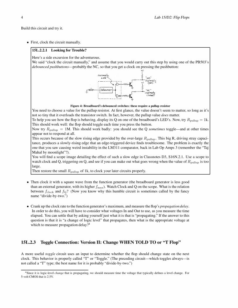
15L.2.2.1 Looking for Trouble?
Here’s a side excursion for the adventurous.We said “clock the circuit manually,” and assume that you would carry out this step by using one of the PB503’sdebounced pushbuttons—probably the NC, so that you get a clock on pressing the pushbutton:
Figure 4: Breadboard’s debounced switches: these require a pullup resistor
You need to choose a value for the pullup resistor. At first glance, the value doesn’t seem to matter, so long as it’snot so tiny that it overloads the transistor switch. In fact, however, the pullup value does matter.To help you see how the flop is behaving, display its Q on one of the breadboard’s LED’s. Now, try Rpullup = 1k.This should work well: the flop should toggle each time you press the button.Now try Rpullup = 1M. This should work badly: you should see the Q sometimes toggle—and at other timesappear not to respond at all.This occurs because of the slow rising edge provided by the over-large Rpullup . This big R, driving stray capaci-tance, produces a slowly-rising edge that an edge-triggered device finds troublesome. The problem is exactly theone that you saw causing weird instability in the LM311 comparator, back in Lab Op Amps 3 (remember the “TajMahal by moonlight”?).You will find a scope image detailing the effect of such a slow edge in Classnotes D3, S16N.2.1. Use a scope towatch clock and Q, triggering on Q, and see if you can make out what goes wrong when the value of Rpullup is toolarge.Then restore the small Rpullup of 1k, to clock your later circuits properly.
• Then clock it with a square wave from the function generator (the breadboard generator is less goodthan an external generator, with its higher fmax). Watch Clock and Q on the scope. What is the relationbetween fclock and fQ? (Now you know why this humble circuit is sometimes called by the fancyname “divide-by-two.”)
• Crank up the clock rate to the function generator’s maximum, and measure theflop’s propagationdelay.In order to do this, you will have to consider what voltages In and Out to use, as you measure the timeelapsed. You can settle that by asking yourself just what it is that is “propagating.” If the answer to thisquestion is that it is “a change of logic level” that propagates, then what is the appropriate voltage atwhich to measure propagation delay?4
15L.2.3 Toggle Connection: Version II: Change WHEN TOLD TO or “T Flop”
A more useful toggle circuit uses an input to determine whether the flop should change state on the nextclock. This behavior is properly called “T” or “Toggle.” (The preceding circuit—which toggles always—isnot called a “T” type; the best name for it is probably “divide-by-two.”)
4Since it is logic-level change that is propagating, we should measure time the voltage that typically defines a level change. For5-volt CMOS that is 2.5V.
Lab 15/D2: Flip Flops 5
Here’s how the circuit should behave:
“T”
clock
logic
V
D QQn+1+1
Qn n (holds)
Qn n (toggles)
T
0
1
whole circuit formsa T-type flip-flop
Figure 5: T flop behaviorShow how to use an XOR gate and a D flop to make such a “T”-type flop. Note that an XOR can serve as acontrollable inverter if you use one input to the XOR as Signal, the other as Control, as you saw in today’sclass notes.
To exercise your “T” flop, clock it from the function generator, control it with a manual switch, and watchclock and Q on a scope.
Keep this “T” flop set up; we will use it again.
15L.3 Counters: Ripple and SynchronousTime: 30 min.
15L.3.1 Ripple Counter
If you wire a flop to toggle on EVERY clock (the easiest way to do this is with a D flop5), and cascade twosuch flops, so that the Q of one flop drives the clock of the next, you form a “divide by four” circuit. One flopchanges on every clock; the other changes on every-other clock. Evidently, you could extend this scheme soas to form a divide-by-a-lot. Today, we won’t go farther than divide-by-four.
Wire a second D-biting-its-tailflop; cascade the two flops to form just such a “divide-by-four” ripple counter.Show what the circuit looks like:
Divide-by-four ripple counter: made from D’s (your design)
• Watch the counter’s outputs on two LEDs while clocking the circuit at a few Hertz. Does it “divide byfour?” If not, either your circuit or your understanding of this phrase is faulty. Fix whichever one needsfixing.
This counter behaves oddly, in one respect: it counts down. An easy way to make it count UP (or arewe only making it appear to count up?) is just to watch the Q outputs rather than the Q’s. (Ripplecounters usually are built with falling-edge clocks, instead; then the Q’s do count up.)
• Now clock the counter as fast as you can, and watch Clock and first Q0 then Q1 on the scope. Triggeron Q1.
• Watch the two Q’s together and see if you can spot the “rippling” effect that gives the circuit its name:a lag between changes at Q0 and Q1. (If you are using an analog scope, you will have to sweep thescope about as fast as it will go, while clocking the counter fast so as to make the display acceptablybright.)
5You don’t need the fancier “T” behavior, to build a ripple counter. You will need it to make a synchronous counter.
6 Lab 15/D2: Flip Flops
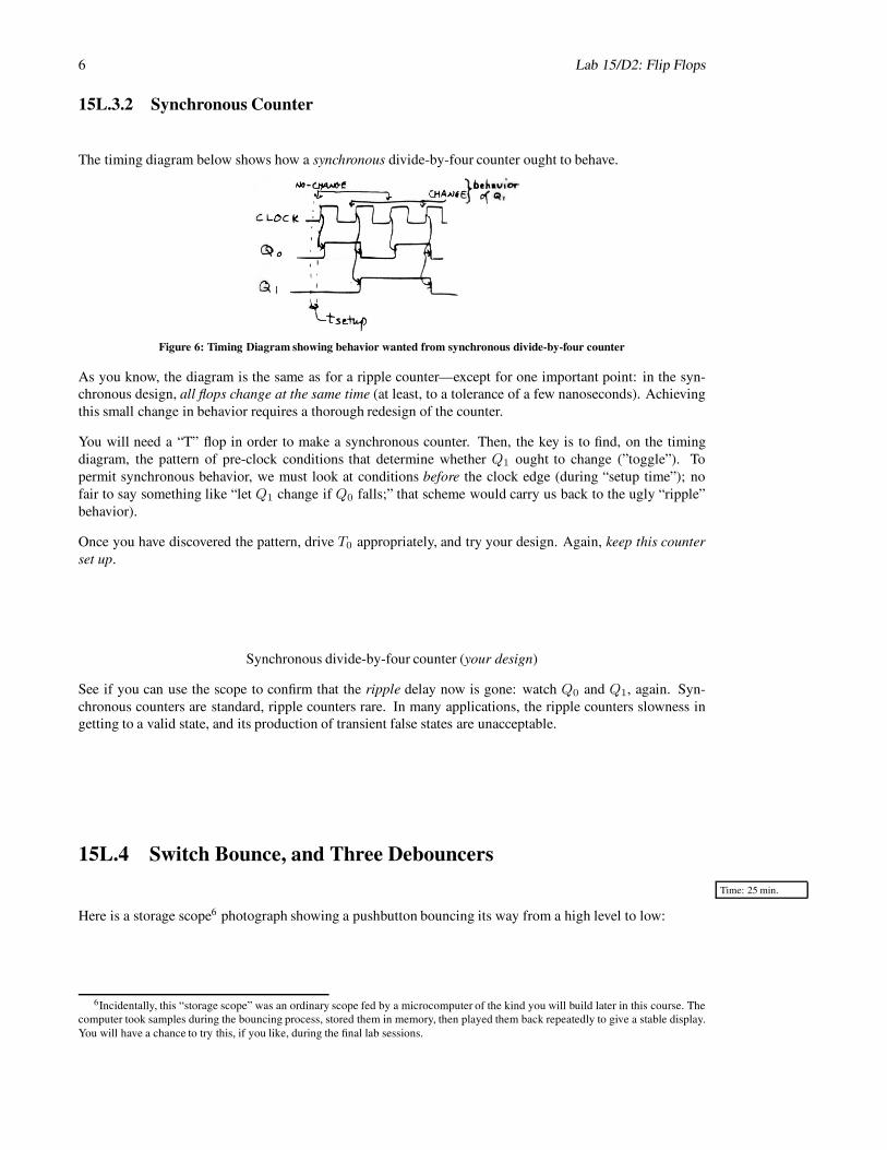
15L.3.2 Synchronous Counter
The timing diagram below shows how a synchronous divide-by-four counter ought to behave.
As you know, the diagram is the same as for a ripple counter—except for one important point: in the syn-chronous design, all flops change at the same time (at least, to a tolerance of a few nanoseconds). Achievingthis small change in behavior requires a thorough redesign of the counter.
You will need a “T” flop in order to make a synchronous counter. Then, the key is to find, on the timingdiagram, the pattern of pre-clock conditions that determine whether Q1 ought to change (”toggle”). Topermit synchronous behavior, we must look at conditions before the clock edge (during “setup time”); nofair to say something like “let Q1 change if Q0 falls;” that scheme would carry us back to the ugly “ripple”behavior).
Once you have discovered the pattern, drive T0 appropriately, and try your design. Again, keep this counterset up.
Synchronous divide-by-four counter (your design)
See if you can use the scope to confirm that the ripple delay now is gone: watch Q0 and Q1, again. Syn-chronous counters are standard, ripple counters rare. In many applications, the ripple counters slowness ingetting to a valid state, and its production of transient false states are unacceptable.
15L.4 Switch Bounce, and Three Debouncers
Time: 25 min.
Here is a storage scope6 photograph showing a pushbutton bouncing its way from a high level to low:
6Incidentally, this “storage scope” was an ordinary scope fed by a microcomputer of the kind you will build later in this course. Thecomputer took samples during the bouncing process, stored them in memory, then played them back repeatedly to give a stable display.You will have a chance to try this, if you like, during the final lab sessions.
Lab 15/D2: Flip Flops 7
2ms
Figure 7: Microswitch bouncing from high to low (pulled up through 100k)
To see the harmful effect of switch bounce, clock your divide-by-four counter with a (bouncy-) ordinaryswitch such as a microswitch pushbutton. Watch the counter’s outputs on two LEDs. The bouncing of theswitch is hard to see on an analog scope (easy on a digital), but its effects should be obvious in the erraticbehavior of the counter.
Figure 8: Switch bounce demonstration
15L.4.1 Watching Switch Bounce (Optional: for scope enthusiasts)
Switch bounce is hard to see on an analog scope, because it does not happen periodically and because thebounces in any event do not occur at exactly repeatable points after the switch is pushed. (On a digital scope,on the other hand, freezing an image of recorded switch bounce is dead easy.)
You can see the bounce, at least dimly, however, if you trigger the scope in Normal mode with a sweep rateof about 0.1 ms/cm. You will need some patience, and some fine adjustments of trigger level. Some switchesbounce only feebly. We suggest a nice snap-action switch like the microswitch type.
15L.4.2 Eliminating Switch Bounce: Two MethodsAoE §10.4.1.1
15L.4.2.1 Cross-coupled NANDs as debouncer
Return to the first and simplest flip-flop (which we hope you saved), the cross-coupled NAND latch, alsocalled an “R-S” flop. As input use the bouncy pushbutton. Ground the switch’s common terminal, and makesure to include pullup resistors on both flop inputs (they should be there, still).
Why does the latch—a circuit designed to “remember”—work as a debouncer?7
7It does because bounce makes the inputs revert to their memory state, in which they seemly hold the state into which they werepushed when the particular input earlier went low.
8 Lab 15/D2: Flip Flops
Figure 9: NAND latch as switch debouncer
2- CMOS buffer as debouncer (positive feedback)
Here’s a much simpler way to debounce, when you use a double-throw switch (SPDT) like the one used inthe preceding exercise: just use a non-inverting CMOS gate,8 with its output talking to its input:
+5
HC08 or HCT08
(no bounce visible, n.b.) (clean)
Figure 10: CMOS AND gate as switch debouncer
This one is no fun to watch—because no bounce will be visible, even at the input. Once you see why this isso, you will have understood why this circuit works as a debouncer. What happens, particularly, during thetime when the switch input to the AND is connected to neither +5 nor ground?
3- D-Flop as debouncer; discovering duration of switch bounce
A plain D flop can debounce, if clocked appropriately. Wire up this circuit to test the notion:
9
4
(1/4 74HC175)
bouncyswitch
clock
+51
2
16 15 14 13 12 11 10
+5R
D0 Q3 Q3 D3 D2V
V
V
74HC175
1 2 3 474 XX 175 Quad D register
5 6 7 8
Q2 Q24 (your counter)Q0
Q0 Q0000 D3 D1 Q1 Q1CLR GND
Figure 11: D flop as debouncer
Fig. 11 suggests using one flop of a 4-flop ’175 because you are about to use this part in another circuit.
Start with a high-frequency square wave driving the D-flop clock (say, 100kHz or more). You should seeevidence of bounce in the counter’s misbehavior. Now lower the clock rate to 100Hz. Bounce should ceaseto trouble the counter. Raise the clock frequency till evidence of bounce reappears. Note the clock period(you’ll get the best information by watching the clock on the scope, of course; you’ll get a ball-park frequencyfrom the dial on the function generator). That clock period reveals how long your switch is bouncing.
Lab 15/D2: Flip Flops 9
15L.5 Shift RegisterTime: 30 min.
(This is an important device—but some people will run out of time, around this point. Don’t worry if thishappens to you. The circuit is not hard to understand, even if you don’t get a chance to build it. The digitalone-shot of 15L.5.3 on the following page, based on the shift-register, is used in a later circuit, a “capacitancemeter.” This circuit is described in Lab D3 and also appears among suggested digital projects. But you canbuild all of this later if you find you need the one-shot and don’t have time for it today. Some people will notbuild the C-meter and thus will not need the one-shot.)
Note: Please build the circuit below (a digitally-timed one-shot that evolves from the shift-register) on a private breadboard; you may use thiscircuit next time.
In fig. 12 we use a convenient structure that includes four flops with a common clock. Such a configurationis called a “register,” and here it is applied to the particular use as shift-register. The circuit of fig. 12 delaysthe signal called “IN,” and synchronizes it to the clock. Both effects can be useful. You will use this circuitin a few minutes as a one-shot—a circuit that generates a single pulse in response to a “Trigger” input (here,the signal called “IN”).
Figure 12: Shift register
Clock the circuit with a logic signal from an external function generator; use the breadboard’s oscillator toprovide “IN.” Let fclock be at least 10 × fIN.
15L.5.1 One Flop: Synchronizer
• Use the scope to watch IN, and Q0 (Q of the leftmost flop); trigger the scope on IN.
• What accounts for the jitter in signal Q0?
• Now trigger on clock, instead. Who’s jittery now?
• Which signal is it more reasonable to call jittery or unstable? (Assume that the flops are clocked witha system clock: a signal that times many devices, not just these 4 flip-flops.)9
15L.5.2 Several Flops: Delay• Now watch a later output—Q1, Q2, or Q3, along with IN. (We’ll leave the triggering to you, this time.)
• Note the effect of altering fclock.
8This circuit does not work reliably with TTL; it’s a CMOS special.9Since we treat the clock as the reference timebase, when we trigger on clock we notice the uncertainty of the input waveforms
timing. It makes sense to say that the input is “jittery.”
10 Lab 15/D2: Flip Flops
15L.5.3 Several Flops Plus Some Gates: Double-Barreled One-Shot
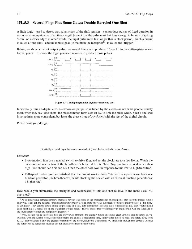
A little logic—used to detect particular states of the shift-register—can produce pulses of fixed duration inresponse to an input pulse of arbitrary length (except that the pulse must last long enough to be sure of getting“seen” on a clock edge: in other words, the input pulse must last longer than a clock period). Such a circuitis called a “one-shot,” and the input signal (to maintain the metaphor10) is called the “trigger.”
Below, we show a pair of output pulses we would like you to produce. If you fill in the shift-register wave-forms, you will discover the logic you need in order to produce those pulses.
Figure 13: Timing diagram for digitally-timed one-shot
Incidentally, this all-digital circuit—whose output pulse is timed by the clock—is not what people usuallymean when they say “one-shot:” the most common form uses an RC to time the pulse width. Such a one-shotis sometimes more convenient, but lacks the great virtue of synchrony with the rest of the digital circuit.
Please draw your design:
Digitally-timed (synchronous) one-shot (double-barreled): your design
Checkout
• Slow-motion: first use a manual switch to drive Trig, and set the clock rate to a few Hertz. Watch theone-shot outputs on two of the breadboard’s buffered LEDs. Take Trig low for a second or so, thenhigh. You should see first one LED then the other flash low, in response to this low-to-high transition.
• Full-speed: when you are satisfied that the circuit works, drive Trig with a square wave from onefunction generator (the breadboard’s) while clocking the device with an external function generator (ata higher rate).
How would you summarize the strengths and weaknesses of this one-shot relative to the more usual RCone-shot?11
10As you may have gathered already, engineers have at least some of the characteristics of good poets: they keep the images simpleand vivid. They call the pedant’s “monostable multivibrator” a “one-shot;” they call the pedant’s “bistable multivibrator” a ”flip-flop,”as you know. They call the active-pullup output stage of a TTL gate”totem pole,” because that’s what it looks like. The synchronizingcolor-burst in a TV signal sits on the waveform’s “back porch.” There’s lots of this vivid imagery in engineering. Can the language ofthe social sciences offer any comparable pleasures?
11Well, in case you’re interested, here are our views: Strength: the digitally-timed one-shot’s great virtue is that its output is syn-chronous with the system clock, so its pulse begins and ends at a predictable time, shortly after the clock edge, and safely away fromtsetup. The weakness is only the greater complexity of the circuit, relative to a traditional RC-timed one-shot, and the circuit’s latency:the output can be delayed as much as one full clock cycle from the rise of trig.
Lab 15/D2: Flip Flops 11
(lab d2 flops headerfile june14.tex; March 7, 2015)